


D
High-Performance Static CMOS Technology
D
Includes the T320C2xLP Core CPU
– Object Compatible With the TMS320C2xx
– Source Code Compatible With
TMS320C25
– Upwardly Compatible With TMS320C5x
– 132-Pin Plastic Quad Flat Package
(PQ Suffix)
– 50-ns Instruction Cycle Time
D
Industrial and Automotive Temperature
Available
D
Memory
– 544 Words × 16 Bits of On-Chip
Data/Program Dual-Access RAM
– 16K Words × 16 Bits of On-Chip Program
ROM (’C240)/Flash EEPROM (’F240)
– 224K Words × 16 Bits of Total Memory
Address Reach (64K Data, 64K Program
and 64K I/O, and 32K Global Memory
Space)
D
Event-Manager Module
– 12 Compare/Pulse-Width Modulation
(PWM) Channels
– Three 16-Bit General-Purpose Timers
With Six Modes, Including Continuous
Upand Up/Down Counting
– Three 16-Bit Full-Compare Units With
Deadband
– Three 16-Bit Simple-Compare Units
– Four Capture Units (Two With
Quadrature Encoder-Pulse Interface
Capability)
TMS320C240, TMS320F240
DSP CONTROLLERS
SPRS042D – OCTOBER 1996 – REVISED NOVEMBER 1998
D
Dual 10-Bit Analog-to-Digital Conversion
Module
D
28 Individually Programmable, Multiplexed
I/O Pins
D
Phase-Locked-Loop (PLL)-Based Clock
Module
D
Watchdog Timer Module (With Real-Time
Interrupt)
D
Serial Communications Interface (SCI)
Module
D
Serial Peripheral Interface (SPI) Module
D
Six External Interrupts (Power Drive
Protect, Reset, NMI, and Three Maskable
Interrupts)
D
Four Power-Down Modes for Low-Power
Operation
D
Scan-Based Emulation
D
Development Tools Available:
– Texas Instruments (TI) ANSI
C Compiler, Assembler/Linker, and
C-Source Debugger
– Scan-Based Self-Emulation (XDS510)
– Third-Party Digital Motor Control and
Fuzzy-Logic Development Support
description
The TMS320C240 and TMS320F240 devices are the first members of a new family of DSP controllers based
on the TMS320C2xx generation of 16-bit fixed-point digital signal processors (DSPs). Unless otherwise noted,
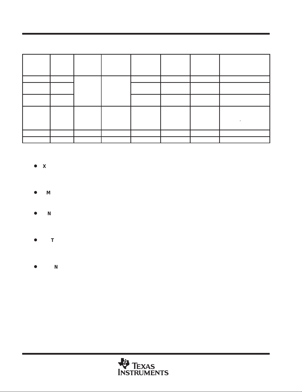
the term ’x240 refers to both the TMS320C240 and the TMS320F240. Table 1 provides a comparison of the
features of each device. The only difference between these two devices is the type of program memory: the
’C240 contains 16K words of ROM and the ’F240 contains 16K words of flash. This new family is optimized for
digital motor/motion control applications. The DSP controllers combine the enhanced TMS320 architectural
design of the ’C2xLP core CPU for low-cost, high-performance processing capabilities and several advanced
peripherals optimized for motor/motion control applications. These peripherals include the event manager
module, which provides general-purpose timers and compare registers to generate up to 12 PWM outputs, and
a dual10-bit analog-to-digital converter (ADC), which can perform two simultaneous conversions within 6.1 µs.
See the functional block diagram.
Please be aware that an important notice concerning availability, standard warranty, and use in critical applications of
Texas Instruments semiconductor products and disclaimers thereto appears at the end of this data sheet.
TI and XDS510 are trademarks of Texas Instruments Incorporated.
PRODUCTION DATA information is current as of publication date.
Products conform to specifications per the terms of Texas Instruments
standard warranty. Production processing does not necessarily include
testing of all parameters.
POST OFFICE BOX 1443 • HOUSTON, TEXAS 77251–1443
Copyright 1998, Texas Instruments Incorporated
1

TMS320C240, TMS320F240
DSP CONTROLLERS
SPRS042D – OCTOBER 1996 – REVISED NOVEMBER 1998
description 1. . . . . . . . . . . . . . . . . . . . . . . . . . . . . . . . . . . . . . . . . . . . . . . . . . . . . . . .
PQ Package (Top View) 5. . . . . . . . . . . . . . . . . . . . . . . . . . . . . . . . . . . . . . . . . . . . .
terminal functions 6. . . . . . . . . . . . . . . . . . . . . . . . . . . . . . . . . . . . . . . . . . . . . . . . . .
functional block diagram 12. . . . . . . . . . . . . . . . . . . . . . . . . . . . . . . . . . . . . . . . . . .
architectural overview 13. . . . . . . . . . . . . . . . . . . . . . . . . . . . . . . . . . . . . . . . . . . . . .
system-level functions 13. . . . . . . . . . . . . . . . . . . . . . . . . . . . . . . . . . . . . . . . . . . . .
device memory map 13. . . . . . . . . . . . . . . . . . . . . . . . . . . . . . . . . . . . . . . . . . . . . . .
peripheral memory map 15. . . . . . . . . . . . . . . . . . . . . . . . . . . . . . . . . . . . . . . . . . .
digital I/O and shared pin functions 16. . . . . . . . . . . . . . . . . . . . . . . . . . . . . . . . . .
description of group1 shared I/O pins 16. . . . . . . . . . . . . . . . . . . . . . . . . . . . .
description of group2 shared I/O pins 18. . . . . . . . . . . . . . . . . . . . . . . . . . . . .
digital I/O control registers 18. . . . . . . . . . . . . . . . . . . . . . . . . . . . . . . . . . . . . . . . .
device reset and interrupts 18. . . . . . . . . . . . . . . . . . . . . . . . . . . . . . . . . . . . . . . . .
reset 19. . . . . . . . . . . . . . . . . . . . . . . . . . . . . . . . . . . . . . . . . . . . . . . . . . . . . . . . . .
hardware-generated interrupts 20. . . . . . . . . . . . . . . . . . . . . . . . . . . . . . . . . . .
external interrupts 26. . . . . . . . . . . . . . . . . . . . . . . . . . . . . . . . . . . . . . . . . . . . . .
clock generation 27. . . . . . . . . . . . . . . . . . . . . . . . . . . . . . . . . . . . . . . . . . . . . . . . . .
low-power modes 29. . . . . . . . . . . . . . . . . . . . . . . . . . . . . . . . . . . . . . . . . . . . . . . . .
functional block diagram of the TMS320x240 DSP CPU 30. . . . . . . . . . . . . . .
’x240 DSP core CPU 33. . . . . . . . . . . . . . . . . . . . . . . . . . . . . . . . . . . . . . . . . . . . . . . .
status and control registers 33. . . . . . . . . . . . . . . . . . . . . . . . . . . . . . . . . . . . . . . .
central processing unit 34. . . . . . . . . . . . . . . . . . . . . . . . . . . . . . . . . . . . . . . . . . . . .
input scaling shifter 34. . . . . . . . . . . . . . . . . . . . . . . . . . . . . . . . . . . . . . . . . . . . .
multiplier 34. . . . . . . . . . . . . . . . . . . . . . . . . . . . . . . . . . . . . . . . . . . . . . . . . . . . . .
central arithmetic logic unit 36. . . . . . . . . . . . . . . . . . . . . . . . . . . . . . . . . . . . . .
accumulator 37. . . . . . . . . . . . . . . . . . . . . . . . . . . . . . . . . . . . . . . . . . . . . . . . . . .
auxiliary registers and auxiliary-register arithmetic unit (ARAU) 37. . . . . . . . .
internal memory 37. . . . . . . . . . . . . . . . . . . . . . . . . . . . . . . . . . . . . . . . . . . . . . . . . . .
dual-access RAM (DARAM) 37. . . . . . . . . . . . . . . . . . . . . . . . . . . . . . . . . . . . . . . .
ROM (TMS320C240 only) 38. . . . . . . . . . . . . . . . . . . . . . . . . . . . . . . . . . . . . . . . .
flash EEPROM (TMS320F240 only) 38. . . . . . . . . . . . . . . . . . . . . . . . . . . . . . . . .
flash serial loader 38. . . . . . . . . . . . . . . . . . . . . . . . . . . . . . . . . . . . . . . . . . . . . .
flash control mode register 38. . . . . . . . . . . . . . . . . . . . . . . . . . . . . . . . . . . . . . .
peripherals 39. . . . . . . . . . . . . . . . . . . . . . . . . . . . . . . . . . . . . . . . . . . . . . . . . . . . . . . .
external memory interface 39. . . . . . . . . . . . . . . . . . . . . . . . . . . . . . . . . . . . . . . . .
Contents
INTRODUCTION
DETAILED DESCRIPTION
2
POST OFFICE BOX 1443 • HOUSTON, TEXAS 77251–1443

TMS320C240, TMS320F240
DSP CONTROLLERS
SPRS042D – OCTOBER 1996 – REVISED NOVEMBER 1998
Contents
DETAILED DESCRIPTION (continued)
event-manager (EV) module 40. . . . . . . . . . . . . . . . . . . . . . . . . . . . . . . . . . . . .
general-purpose (GP) timers 40. . . . . . . . . . . . . . . . . . . . . . . . . . . . . . . . . .
full compare units 42. . . . . . . . . . . . . . . . . . . . . . . . . . . . . . . . . . . . . . . . . . .
programmable-deadband generator 42. . . . . . . . . . . . . . . . . . . . . . . . . . . .
simple compares 42. . . . . . . . . . . . . . . . . . . . . . . . . . . . . . . . . . . . . . . . . . . . .
compare/PWM waveform generation 42. . . . . . . . . . . . . . . . . . . . . . . . . . . .
compare/PWMs characteristics 42
capture unit 42. . . . . . . . . . . . . . . . . . . . . . . . . . . . . . . . . . . . . . . . . . . . . . . . . .
quadrature-encoder pulse (QEP) circuit 43. . . . . . . . . . . . . . . . . . . . . . . . .
analog-to-digital converter (ADC) module 43. . . . . . . . . . . . . . . . . . . . . . . . . .
serial peripheral interface (SPI) module 45. . . . . . . . . . . . . . . . . . . . . . . . . . . .
serial communications interface (SCI) module 47. . . . . . . . . . . . . . . . . . . . . .
watchdog (WD) and real-time interrupt (RTI) module 49. . . . . . . . . . . . . . . .
scan-based emulation 51. . . . . . . . . . . . . . . . . . . . . . . . . . . . . . . . . . . . . . . . . . . .
TMS320x240 instruction set 51. . . . . . . . . . . . . . . . . . . . . . . . . . . . . . . . . . . . . . .
addressing modes 51. . . . . . . . . . . . . . . . . . . . . . . . . . . . . . . . . . . . . . . . . . . . . .
repeat feature 51. . . . . . . . . . . . . . . . . . . . . . . . . . . . . . . . . . . . . . . . . . . . . . . . . .
instruction set summary 52. . . . . . . . . . . . . . . . . . . . . . . . . . . . . . . . . . . . . . . . .
development support 58. . . . . . . . . . . . . . . . . . . . . . . . . . . . . . . . . . . . . . . . . . . . .
device and development-support tool nomenclature 59. . . . . . . . . . . . . . . .
documentation support 60. . . . . . . . . . . . . . . . . . . . . . . . . . . . . . . . . . . . . . . . . . .
. . . . . . . . . . . . . . . . . . . . . . . . . . . . . . . . .
ELECTRICAL SPECIFICATIONS
absolute maximum ratings over operating free-air temperature range 61.
recommended operating conditions 61. . . . . . . . . . . . . . . . . . . . . . . . . . . . . . . . .
output current variation with output voltage: SPICE simulation results 62
elec characteristics over recommended oper free-air temperature range 62
signal transition levels 63. . . . . . . . . . . . . . . . . . . . . . . . . . . . . . . . . . . . . . . . . . . . .
timing parameter symbology 65. . . . . . . . . . . . . . . . . . . . . . . . . . . . . . . . . . . . . . . .
general notes on timing parameters 65. . . . . . . . . . . . . . . . . . . . . . . . . . . . . . . . .
clock options 66. . . . . . . . . . . . . . . . . . . . . . . . . . . . . . . . . . . . . . . . . . . . . . . . . . . . . .
timings with the PLL circuit disabled 66. . . . . . . . . . . . . . . . . . . . . . . . . . . . . . . . .
external reference crystal with PLL-circuit-enabled clock option 67. . . . . . . . .
timings with the PLL circuit enabled 67. . . . . . . . . . . . . . . . . . . . . . . . . . . . . . . . .
low-power mode timings 69. . . . . . . . . . . . . . . . . . . . . . . . . . . . . . . . . . . . . . . . . . .
POST OFFICE BOX 1443 • HOUSTON, TEXAS 77251–1443
3

TMS320C240, TMS320F240
DSP CONTROLLERS
SPRS042D – OCTOBER 1996 – REVISED NOVEMBER 1998
ELECTRICAL SPECIFICATIONS (continued)
Contents
memory and parallel I/O interface
memory and parallel I/O interface
I/O timing variation with load capacitance: SPICE simulation results 75. . .
READY timings 76. . . . . . . . . . . . . . . . . . . . . . . . . . . . . . . . . . . . . . . . . . . . . . . . . . . .
RS and PORESET timings 77. . . . . . . . . . . . . . . . . . . . . . . . . . . . . . . . . . . . . . . . . .
XF, BIO, and MP/MC timings 79. . . . . . . . . . . . . . . . . . . . . . . . . . . . . . . . . . . . . . . .
PWM/CMP timings 80. . . . . . . . . . . . . . . . . . . . . . . . . . . . . . . . . . . . . . . . . . . . . . . . .
capture and QEP timings 81. . . . . . . . . . . . . . . . . . . . . . . . . . . . . . . . . . . . . . . . . . .
interrupt timings 82. . . . . . . . . . . . . . . . . . . . . . . . . . . . . . . . . . . . . . . . . . . . . . . . . . .
general-purpose input/output timings 83. . . . . . . . . . . . . . . . . . . . . . . . . . . . . . .
serial communications interface (SCI) I/O timings 84. . . . . . . . . . . . . . . . . . . .
SPI master mode external timing parameters (clock phase = 0) 85. . . . . . . .
SPI master mode external timing parameters (clock phase = 1) 87. . . . . . . .
SPI slave mode external timing parameters (clock phase = 0) 89. . . . . . . . .
SPI slave mode external timing parameters (clock phase = 1) 91. . . . . . . . .
10-bit dual analog-to-digital converter (ADC) 93. . . . . . . . . . . . . . . . . . . . . . . . .
ADC input pin circuit 94. . . . . . . . . . . . . . . . . . . . . . . . . . . . . . . . . . . . . . . . . . . . . . .
flash EEPROM 96. . . . . . . . . . . . . . . . . . . . . . . . . . . . . . . . . . . . . . . . . . . . . . . . . . . . .
programming operation 96. . . . . . . . . . . . . . . . . . . . . . . . . . . . . . . . . . . . . . . . . . . .
erase operation 96. . . . . . . . . . . . . . . . . . . . . . . . . . . . . . . . . . . . . . . . . . . . . . . . . . .
flash-write operation 96. . . . . . . . . . . . . . . . . . . . . . . . . . . . . . . . . . . . . . . . . . . . . . .
register file compilation 97. . . . . . . . . . . . . . . . . . . . . . . . . . . . . . . . . . . . . . . . . . . .
package drawing, PQ (S-PQFP-G***), PLASTIC QUAD FLATPACK 104. . . . . .
read
timings 71. . . . . . . . . . . . . . . . . . . . . . .
write
timings 73. . . . . . . . . . . . . . . . . . . . . .
4
POST OFFICE BOX 1443 • HOUSTON, TEXAS 77251–1443
TMS320C240, TMS320F240
DSP CONTROLLERS
SPRS042D – OCTOBER 1996 – REVISED NOVEMBER 1998
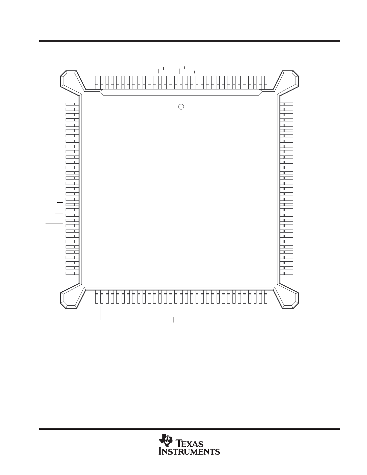
PQ PACKAGE
(TOP VIEW)
V
DV
DD
D10
D11
D12
D13
D14
D15
V
TCK
TDI
TRST
TMS
TDO
RS
READY
MP/MC
EMU0
EMU1/OFF
NMI
PORESET
RESERVED
SCIRXD/IO
SCITXD/IO
SPISIMO/IO
V
DV
DD
SPISOMI/IO
SPICLK/IO
WDDIS
D7
D8
SS
D9
SS
SS
DD
SS
V
D5
D4
D3D6D2
DV
12
13
14
15
16
17
18
19
20
21
22
23
24
25
26
27
28
29
30
31
32
33
34
35
36
37
38
39
40
41
42
43
44
45
46
47
48
†
49
50
525354
555156
SS
DD
D0
CV
D1
11
10
STRBBRR/W
CV
9
867
TMS320C240
TMS320F240
58
59
6067626361
DD
SS
V
DV
234
5
64
65
66
ISDSA15
A14
A13
128
127
126
A12
125
W/R
PS
WE
1
131
129
130
132
695768
70717273747576777879808182
A11
124
A10
123
A9
122
DV
121
DD
SS
V
120
A8A7A6
119
118
117
116
115
114
113
112
111
110
109
108
107
106
105
104
103
102
101
100
99
98
97
96
95
94
93
92
91
90
89
88
87
86
85
84
83
A5
A4
A3
V
SS
A2
A1
A0
TMRCLK/IOPB7
TMRDIR/IOPB6
T3PWM/T3CMP/IOPB5
T2PWM/T2CMP/IOPB4
T1PWM/T1CMP/IOPB3
V
SS
DV
DD
PWM9/CMP9/IOPB2
PWM8/CMP8/IOPB1
PWM7/CMP7/IOPB0
PWM6/CMP6
PWM5/CMP5
PWM4/CMP4
PWM3/CMP3
PWM2/CMP2
PWM1/CMP1
DV
DD
V
SS
ADCIN8/IOPA3
ADCIN9/IOPA2
ADCIN10
ADCIN11
V
SSA
V
REFLO
V
REFHI
V
CCA
XINT1
PDPINT
XINT3/IO
XINT2/IO
SPISTE/IO
†
For the TMS320F240 devices, this pin is V
OSCBYP
DD
SS
DD
VSSV
CV
XTAL2
XTAL1/CLKIN
DV
XF/IOPC2
BIO/IOPC3
CLKOUT/IOPC1
ADCSOC/IOPC0
/WDDIS.
CCP
POST OFFICE BOX 1443 • HOUSTON, TEXAS 77251–1443
CAP1/QEP1/IOPC4
SS
V
CAP3/IOPC6
CAP4/IOPC7
ADCIN0/IOPA0
CAP2/QEP2/IOPC5
ADCIN1/IOPA1
ADCIN2
ADCIN3
ADCIN5
ADCIN4
ADCIN7
ADCIN6
ADCIN15
ADCIN14
ADCIN12
ADCIN13
5
TMS320C240, TMS320F240
TYPE
†
DESCRIPTION
DSP CONTROLLERS
SPRS042D – OCTOBER 1996 – REVISED NOVEMBER 1998
TERMINAL
NAME NO.
EXTERNAL INTERFACE DATA/ADDRESS SIGNALS
A0 (LSB)
A1
A2
A3
A4
A5
A6
A7
A8
A9
A10
A11
A12
A13
A14
A15 (MSB)
D0 (LSB)
D1
D2
D3
D4
D5
D6
D7
D8
D9
D10
D11
D12
D13
D14
D15 (MSB)
DS
PS
IS
READY 36 I
R/W 4 O/Z
STRB 6 O/Z
WE 1 O/Z
W/R 132 O/Z
†
I = input, O = output, Z = high impedance
110
111
112
114
115
116
117
118
119
122
123
124
125
126
127
128
9
10
11
12
15
16
17
18
19
22
23
24
25
26
27
28
129
131
130
O/Z
I/O/Z
O/Z
Parallel address bus A0 [least significant bit (LSB)] through A15 [most significant bit (MSB)]. A15–A0
are multiplexed to address external data/program memory or I/O. A15–A0 are placed in
high-impedance state when EMU1/OFF
modes.
Parallel data bus D0 (LSB) through D15 (MSB). D15–D0 are multiplexed to transfer data between the
TMS320x240 and external data/program memory and I/O space (devices). D15–D0 are placed in the
high-impedance state when not outputting, when in power-down mode, when reset (RS
or when EMU1/OFF
EXTERNAL INTERFACE CONTROL SIGNALS
Data, program, and I/O space select signals. DS, PS, and IS are always high unless low-level asserted
for communication to a particular external space. They are placed in the high-impedance state during
reset, power down, and when EMU1/OFF
Data ready. READY indicates that an external device is prepared for the bus transaction to be
completed. If the device is not ready (READY is low), the processor waits one cycle and checks
READY again.
Read/write signal. R/W indicates transfer direction during communication to an external device. It is
normally in read mode (high), unless low level is asserted for performing a write operation. It is placed
in the high-impedance state during reset, power down, and when EMU1/OFF
Strobe. STRB is always high unless asserted low to indicate an external bus cycle. It is placed in the
high-impedance state during reset, power down, and when EMU1/OFF
Write enable. The falling edge of WE indicates that the device is driving the external data bus
(D15–D0). Data can be latched by an external device on the rising edge of WE
external program, data, and I/O writes. WE
EMU1/OFF
Write/read. W/R is an inverted form of R/W and can connect directly to the output enable of external
devices. W/R
Terminal Functions
is active low and hold their previous states in power-down
) is asserted,
is active low.
is active low.
is active low.
is active low.
. WE is active on all
goes in the high-impedance state following reset and when
is active low.
is placed in the high-impedance state following reset and when EMU1/OFF is active low.
6
POST OFFICE BOX 1443 • HOUSTON, TEXAS 77251–1443
TYPE
†
DESCRIPTION
Analog inputs to the first ADC
Analog inputs to the second ADC
TERMINAL
NAME NO.
EXTERNAL INTERFACE CONTROL SIGNALS (CONTINUED)
BR 5 O/Z
‡
WDDIS
ADCIN2 74 I
ADCIN3 75 I
ADCIN4 76 I
ADCIN5 77 I
ADCIN6 78 I
ADCIN7 79 I
ADCIN10 89 I
ADCIN11 88 I
ADCIN12 83 I
ADCIN13 82 I
ADCIN14 81 I
ADCIN15 80 I
ADCIN0/IOPA0 72 I/O
ADCIN1/IOPA1 73 I/O
ADCIN9/IOPA2 90 I/O
ADCIN8/IOPA3 91 I/O
PWM7/CMP7/IOPB0 100 I/O/Z
PWM8/CMP8/IOPB1 101 I/O/Z
PWM9/CMP9/IOPB2 102 I/O/Z
†
I = input, O = output, Z = high impedance
‡
For the TMS320F240 devices, this pin is V
50 I
TMS320C240, TMS320F240
DSP CONTROLLERS
SPRS042D – OCTOBER 1996 – REVISED NOVEMBER 1998
Terminal Functions (Continued)
Bus request. BR is asserted during access of external global data memory space. BR can be
used to extend the data memory address space by up to 32K words. BR
high-impedance state during reset, power down, and when EMU1/OFF
Flash-programming voltage supply. If V
ENTIRE on-chip flash memory block—that is, for programming the flash. If V
WRITE/ERASE of the flash memory is not allowed, thereby protecting the entire memory block
from being overwritten. WDDIS also functions as a hardware watchdog disable. The watchdog
timer is disabled when V
ADC INPUTS (UNSHARED)
p
p
BIT I/O AND SHARED FUNCTIONS PINS
Bidirectional digital I/O.
Analog input to the first ADC.
ADCIN0/IOPA0 is configured as a digital input by all device resets.
Bidirectional digital I/O.
Analog input to the first ADC.
ADCIN1/IOPA1 is configured as a digital input by all device resets.
Bidirectional digital I/O.
Analog input to the second ADC.
ADCIN9/IOPA2 is configured as a digital input by all device resets.
Bidirectional digital I/O.
Analog input to the second ADC.
ADCIN8/IOPA3 is configured as a digital input by all device resets.
Bidirectional digital I/O. Simple compare/PWM 1 output. The state of PWM7/CMP7/IOPB0 is
determined by the simple compare/PWM and the simple action control register (SACTR). It
goes to the high-impedance state when unmasked PDPINT
PWM7/CMP7/IOPB0 is configured as a digital input by all device resets.
Bidirectional digital I/O. Simple compare/PWM 2 output. The state of PWM8/CMP8/IOPB1 is
determined by the simple compare/PWM and the SACTR. It goes to the high-impedance state
when unmasked PDPINT
by all device resets.
Bidirectional digital I/O. Simple compare/PWM 3 output. The state of PWM9/CMP9/IOPB2 is
determined by the simple compare/PWM and SACTR. It goes to the high-impedance state
when unmasked PDPINT
by all device resets.
CCP/WDDIS
.
/WDDIS = 5 V and bit 6 in WDCR is set to 1.
CCP
goes active low. PWM8/CMP8/IOPB1 is configured as a digital input
goes active low. PWM9/CMP9/IOPB2 is configured as a digital input
= 5 V, then WRITE/ERASE can be made to the
CCP
goes in the
is active low.
CCP
goes active low.
= 0 V , then
POST OFFICE BOX 1443 • HOUSTON, TEXAS 77251–1443
7
TMS320C240, TMS320F240
TYPE
†
DESCRIPTION
DSP CONTROLLERS
SPRS042D – OCTOBER 1996 – REVISED NOVEMBER 1998
Terminal Functions (Continued)
TERMINAL
NAME NO.
BIT I/O AND SHARED FUNCTIONS PINS (CONTINUED)
T1PWM/T1CMP/
IOPB3
T2PWM/T2CMP/
IOPB4
T3PWM/T3CMP/
IOPB5
TMRDIR/IOPB6 108 I/O
TMRCLK/IOPB7 109 I/O
ADCSOC/IOPC0 63 I/O
CAP1/QEP1/IOPC4 67 I/O
CAP2/QEP2/IOPC5 68 I/O
CAP3/IOPC6 69 I/O
CAP4/IOPC7 70 I/O
XF/IOPC2 65 I/O
BIO/IOPC3 66 I/O
CLKOUT/IOPC1 64 I/O
SCITXD/IO 44 I/O
SCIRXD/IO 43 I/O
†
I = input, O = output, Z = high impedance
105 I/O/Z
106 I/O/Z
107 I/O/Z
SERIAL COMMUNICATIONS INTERFACE (SCI) AND BIT I/O PINS
Bidirectional digital I/O. Timer 1 compare output. T1PWM/T1CMP/IOPB3 goes to the highimpedance state when unmasked PDPINT
input by all device resets.
Bidirectional digital I/O. Timer 2 compare output. T2PWM/T2CMP/IOPB4 goes to the highimpedance state when unmasked PDPINT
input by all device resets.
Bidirectional digital I/O. Timer 3 compare output. T3PWM/T3CMP/IOPB5 goes to the highimpedance state when unmasked PDPINT
input by all device resets.
Bidirectional digital I/O. Direction signal for the timers. Up-counting direction if TMRDIR/IOPB6
is low, down-counting direction if this pin is high.
This pin is configured as a digital input by all device resets.
Bidirectional digital I/O.
External clock input for general-purpose timers.
This pin is configured as a digital input by all device resets.
Bidirectional digital I/O.
External start of conversion input for ADC.
This pin is configured as a digital input by all device resets.
Bidirectional digital I/O.
Capture 1 or QEP 1 input.
This pin is configured as a digital input by all device resets.
Bidirectional digital I/O.
Capture 2 or QEP 2 input.
This pin is configured as a digital input by all device resets.
Bidirectional digital I/O.
Capture 3 input.
This pin is configured as a digital input by all device resets.
Bidirectional digital I/O.
Capture 4 input.
This pin is configured as a digital input by all device resets.
Bidirectional digital I/O. External flag output (latched software-programmable signal). XF is
used for signaling other processors in multiprocessing configurations or as a general-purpose
output pin. This pin is configured as an external flag output by all device resets.
Bidirectional digital I/O. Branch control input. BIO is polled by the BIOZ instruction. If BIO is low,
the CPU executes a branch. If BIO
as a branch-control input by all device resets.
Bidirectional digital I/O. Clock output. Clock output is selected by the CLKSRC bits in the
SYSCR register. This pin is configured as a DSP clock output by a power-on reset.
SCI asynchronous serial port transmit data, or general-purpose bidirectional I/O. This pin is
configured as a digital input by all device resets.
SCI asynchronous serial port receive data, or general-purpose bidirectional I/O. This pin is
configured as a digital input by all device resets.
goes active low. This pin is configured as a digital
goes active low. This pin is configured as a digital
goes active low. This pin is configured as a digital
is not used , it should be pulled high. This pin is configured
8
POST OFFICE BOX 1443 • HOUSTON, TEXAS 77251–1443
TYPE
†
DESCRIPTION
Terminal Functions (Continued)
TERMINAL
NAME NO.
SERIAL PERIPHERAL INTERFACE (SPI) AND BIT I/O PINS
SPISIMO/IO 45 I/O
SPISOMI/IO 48 I/O
SPICLK/IO 49 I/O
SPISTE/IO 51 I/O
PWM1/CMP1
PWM2/CMP2
PWM3/CMP3
PWM4/CMP4
PWM5/CMP5
PWM6/CMP6
RS 35 I/O
MP/MC 37 I
NMI 40 I
PORESET 41 I
XINT1 53 I External user interrupt no. 1
XINT2/IO 54 I/O
XINT3/IO 55 I/O
PDPINT 52 I
XTAL2 57 O
XTAL1/CLKIN 58 I/Z
OSCBYP 56 I Bypass oscillator if low
†
I = input, O = output, Z = high impedance
94
95
96
97
98
99
O/Z
SPI slave in, master out , or general-purpose bidirectional I/O. This pin is configured as a digital
input by all device resets.
SPI slave out, master in, or general-purpose bidirectional I/O. This pin is configured as a digital
input by all device resets.
SPI clock, or general-purpose bidirectional I/O. This pin is configured as a digital input by all
device resets.
SPI slave transmit enable (optional), or general-purpose bidirectional I/O. This pin is configured
as a digital input by all device resets.
COMPARE SIGNALS
Compare units compare or PWM outputs. The state of these pins is determined by the
compare/PWM and the full action control register (ACTR). CMP1–CMP6 go to the highimpedance state when unmasked PDPINT
INTERRUPT AND MISCELLANEOUS SIGNALS
Reset input. RS causes the TMS320x240 to terminate execution and sets PC = 0. When RS
is brought to a high level, execution begins at location zero of program memory. RS af fects (or
sets to zero) various registers and status bits.
MP/MC (microprocessor/microcomputer) select. If MP/MC is low, internal program memory is
selected. If it is high, external program memory is selected.
Nonmaskable interrupt. When NMI is activated, the device is interrupted regardless of the state
of the INTM bit of the status register. NMI has programmable polarity.
Power-on reset. PORESET causes the TMS320x240 to terminate execution and sets PC = 0.
When PORESET
memory. PORESET
tion, PORESET
External user interrupt no. 2. General-purpose bidirectional I/O. This pin is configured as a
digital input by all device resets.
External user interrupt no. 3. General-purpose bidirectional I/O. This pin is configured as a
digital input by all device resets.
Maskable power-drive protection interrupt. If PDPINT is unmasked and it goes active low, the
timer compare outputs immediately go to the high-impedance state.
PLL oscillator output. XT AL2 is tied to one side of a reference crystal when the device is in PLL
mode (CLKMD[1:0] = 1x, CKCR0.7–6). This pin can be left unconnected in oscillator bypass
mode (OSCBYP
low.
PLL oscillator input. XTAL1/CLKIN is tied to one side of a reference crystal in PLL mode
(CLKMD[1:0] = 1x, CKCR0.7–6), or is connected to an external clock source in oscillator
bypass mode (OSCBYP
is brought to a high level, execution begins at location zero of program
affects (or sets to zero) the same registers and status bits as RS. In addi-
initializes the PLL control registers.
CLOCK SIGNALS
≤ VIL). This pin goes in the high-impedance state when EMU1/OFF is active
TMS320C240, TMS320F240
DSP CONTROLLERS
SPRS042D – OCTOBER 1996 – REVISED NOVEMBER 1998
goes active low, and when reset (RS) is asserted.
≤ VIL).
POST OFFICE BOX 1443 • HOUSTON, TEXAS 77251–1443
9
TMS320C240, TMS320F240
TYPE
†
DESCRIPTION
V
I
Digital logic ground reference
DV
I
Digital I/O logic suppl
oltage
CV
I
Digital core logic suppl
oltage
DSP CONTROLLERS
SPRS042D – OCTOBER 1996 – REVISED NOVEMBER 1998
Terminal Functions (Continued)
TERMINAL
NAME NO.
CV
SS
SS
8 I Digital core logic ground reference
3
14
20
29
46
59
61
71
92
104
113
120
SUPPLY SIGNALS
V
SSA
DD
DD
V
CCA
V
REFHI
V
REFLO
TCK 30 I
TDI 31 I
TDO 34 O/Z
TMS 33 I
†
I = input, O = output, Z = high impedance
87 I Analog ground reference
2
13
21
47
62
93
103
121
7
60
84 I Analog supply voltage
85 I ADC analog voltage reference high
86 I ADC analog voltage reference low
pp
y v
pp
y v
TEST SIGNALS
IEEE standard test clock. TCK is normally a free-running clock signal with a 50% duty cycle. The
changes on test-access port (TAP) input signals (TMS and TDI) are clocked into the TAP controller,
instruction register, or selected test data register of the ’C2xx core on the rising edge of TCK. Changes
at the TAP output signal (TDO) occur on the falling edge of TCK.
IEEE standard test data input (TDI). TDI is clocked into the selected register (instruction or data) on
a rising edge of TCK.
IEEE standard test data output (TDO). The contents of the selected register (instruction or data) are
shifted out of TDO on the falling edge of TCK. TDO is in the high-impedance state when OFF
low.
IEEE standard test mode select. This serial control input is clocked into the TAP controller on the rising
edge of TCK.
is active
10
POST OFFICE BOX 1443 • HOUSTON, TEXAS 77251–1443
TYPE
†
DESCRIPTION
TERMINAL
NAME NO.
TRST 32 I
EMU0 38 I/O/Z
EMU1/OFF 39 I/O/Z
RESERVED 42 I
†
I = input, O = output, Z = high impedance
TMS320C240, TMS320F240
DSP CONTROLLERS
SPRS042D – OCTOBER 1996 – REVISED NOVEMBER 1998
Terminal Functions (Continued)
TEST SIGNALS (CONTINUED)
IEEE standard test reset. TRST, when active low, gives the scan system control of the operations of
the device. If this signal is not connected or driven low, the device operates in its functional mode, and
the test reset signals are ignored.
Emulator pin 0. When TRST is driven low, EMU0 must be high for activation of the /OFF condition.
When TRST
as input/output through the scan.
Emulator pin 1/disable all outputs. When TRST is driven high, EMU1/OFF is used as an interrupt to
or from the emulator system and is defined as input/output through JTAG scan. When TRST
low, this pin is configured as OFF
high-impedance state. OFF
multiprocessing applications); therefore, for OFF
low, EMU0 = high, EMU1/OFF
Reserved for test. This pin has an internal pulldown and must be left unconnected for the ’F240. On
the ’C240, this pin is a no connect.
is driven high, EMU0 is used as an interrupt to or from the emulator system and is defined
is driven
. When EMU1/OFF is active low, it puts all output drivers in the
is used exclusively for testing and emulation purposes (not for
condition, the following conditions apply: TRST =
= low.
POST OFFICE BOX 1443 • HOUSTON, TEXAS 77251–1443
11
TMS320C240, TMS320F240
DSP CONTROLLERS
SPRS042D – OCTOBER 1996 – REVISED NOVEMBER 1998
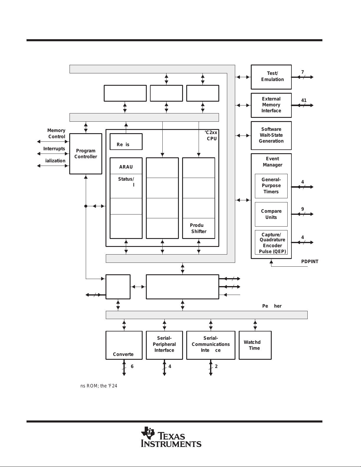
functional block diagram
Data Bus
Memory
Control
Interrupts
Initialization
Program Bus
Program
Controller
EEPROM
Instruction
Register
ARAU
Status/
Control
Registers
Auxiliary
Registers
Memory-
Mapped
Registers
†
DARAMROM or Flash
B0
Input
Shifter
ALU
Accumulator
Output
Shifter
DARAM
B1/B2
Multiplier
TREG
PREG
Product
Shifter
’C2xx
CPU
Test/
Emulation
External
Memory
Interface
Software
Wait-State
Generation
Event
Manager
General-
Purpose
Timers
Compare
Units
Capture/
Quadrature
Encoder
Pulse (QEP)
7
41
4
9
4
Clock
3
†
The ’C240 device contains ROM; the ’F240 device contains Flash EEPROM.
Module
Dual 10-Bit
Analog-
to-Digital
Converter
System-Interface
Module
Serial-
Peripheral
Interface
4
Serial-
Communications
Interface
216
4
Interrupts
20
Digital Input/Output
Reset
Watchdog
Timer
PDPINT
Peripheral Bus
12
POST OFFICE BOX 1443 • HOUSTON, TEXAS 77251–1443
(V)
(ns)
PIN COUNT
description (continued)
TMS320C240, TMS320F240
DSP CONTROLLERS
SPRS042D – OCTOBER 1996 – REVISED NOVEMBER 1998
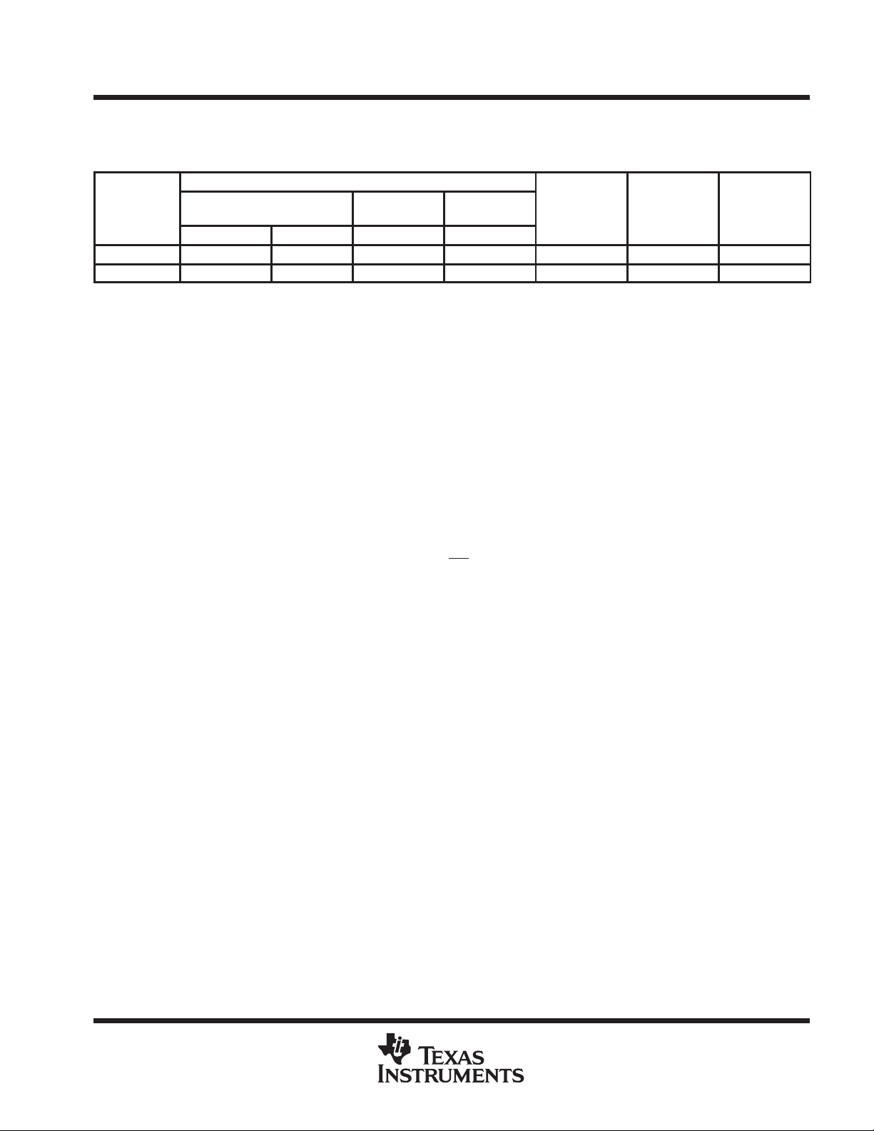
Table 1. Characteristics of the ’x240 DSP Controllers
ON-CHIP MEMORY (WORDS)
TMS320x240
DEVICES
DATA DATA/PROG PROG PROG
TMS320C240 288 256 16K – 5 50 PQ 132–P
TMS320F240 288 256 – 16K 5 50 PQ 132–P
RAM ROM
FLASH
EEPROM
POWER
SUPPLY
CYCLE
TIME
PACKAGE
TYPE
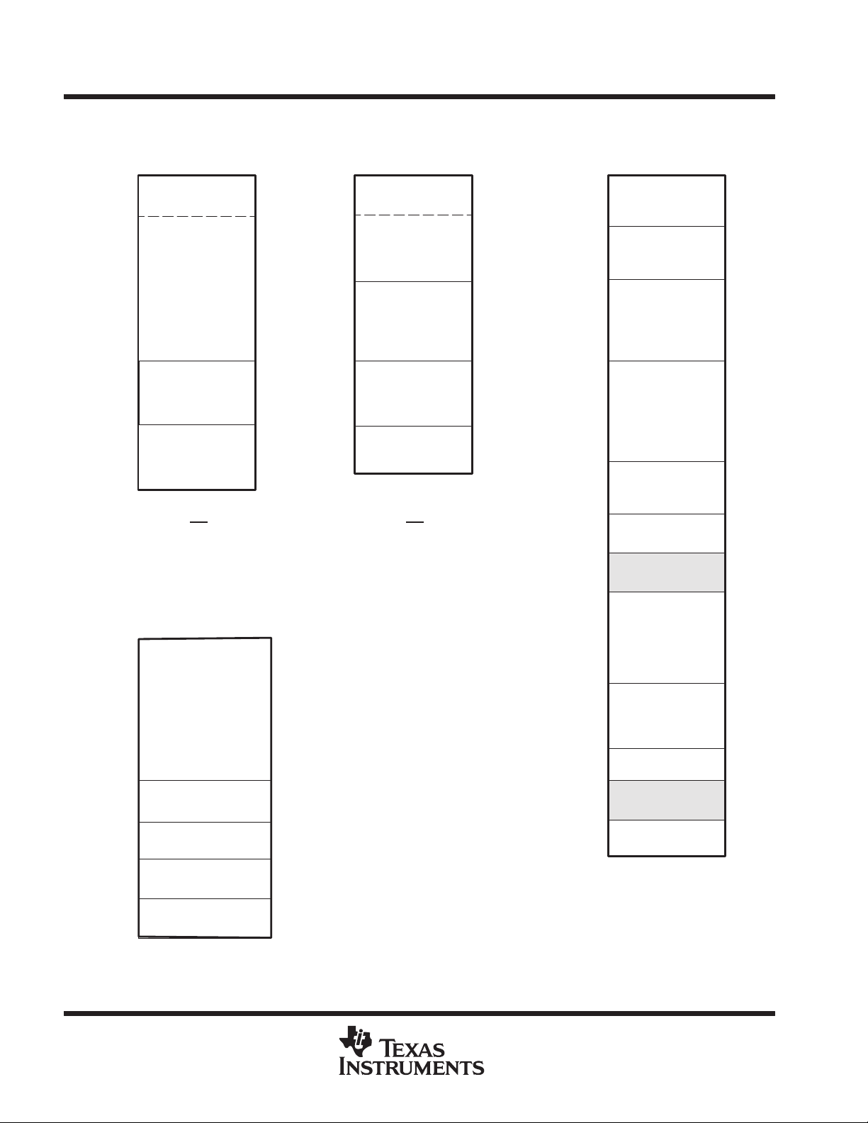
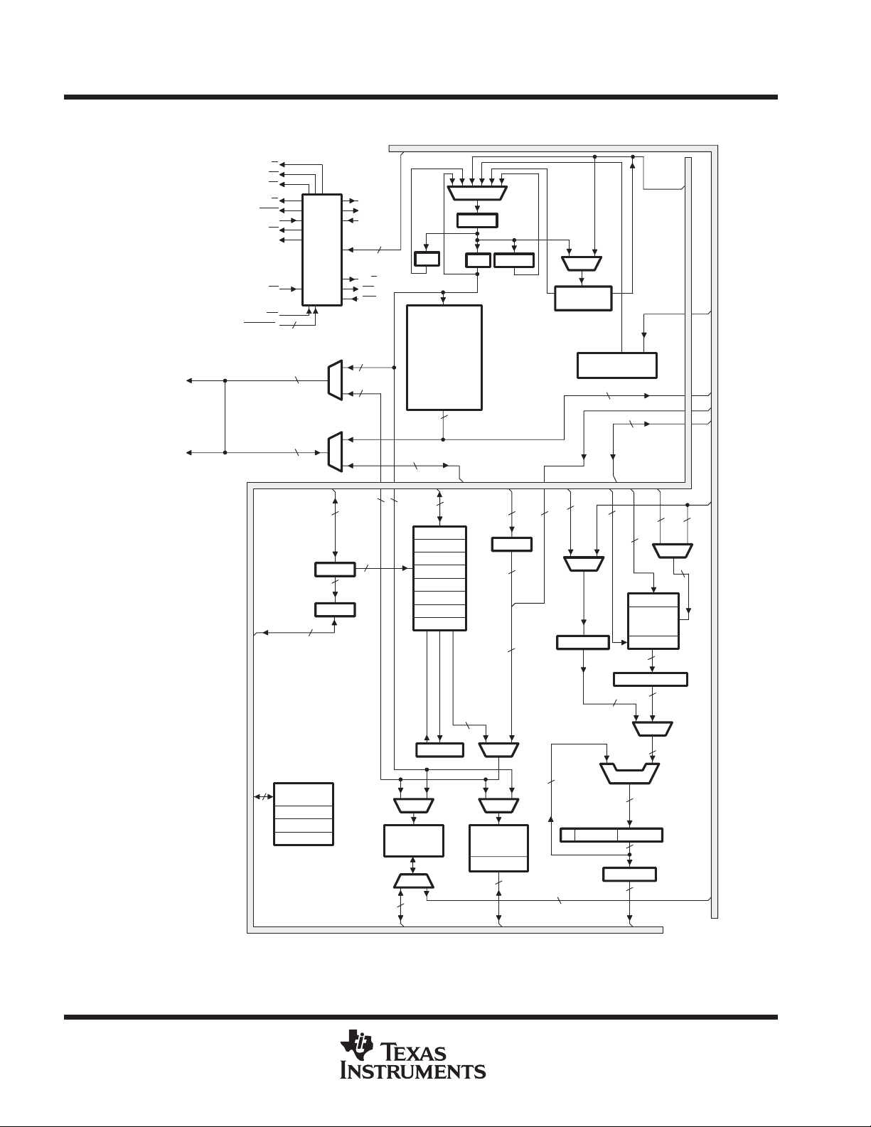
architectural overview
The functional block diagram provides a high-level description of each component in the ’x240 DSP controller.
The TMS320x240 devices are composed of three main functional units: a ’C2xx DSP core, internal memory,
and peripherals. In addition to these three functional units, there are several system-level features of the ’x240
that are distributed. These system features include the memory map, device reset, interrupts, digital
input/output (I/O), clock generation, and low-power operation.
system-level functions
device memory map
The TMS320x240 implements three separate address spaces for program memory, data memory, and I /O.
Each space accommodates a total of 64K 16-bit words. Within the 64K words of data space, the 256 to
32K words at the top of the address range can be defined to be external global memory in increments of powers
of two, as specified by the contents of the global memory allocation register (GREG). Access to global memory
is arbitrated using the global memory bus request (BR) signal.
On the ’x240, the first 96 (0–5Fh) data memory locations are either allocated for memory-mapped registers or
are reserved. This memory-mapped register space contains various control and status registers including those
for the CPU.
All the on-chip peripherals of the ’x240 device are mapped into data memory space. Access to these registers
is made by the CPU instructions addressing their data-memory locations. Figure 1 shows the memory map.
POST OFFICE BOX 1443 • HOUSTON, TEXAS 77251–1443
13
TMS320C240, TMS320F240
DSP CONTROLLERS
SPRS042D – OCTOBER 1996 – REVISED NOVEMBER 1998
device memory map (continued)
Program
Program
Data
Hex
0000
003F
0040
FDFF
FE00
On-Chip DARAM B0
External (CNF = 0)
FEFF
FF00
FFFF
Microprocessor
Hex
0000
FEFF
FF00
FF0E
FF0F
FF10
FFFE
FFFF
Wait-state Generator
Interrupts
(External)
External
(CNF = 1)
or
Reserved
= 1
MP/MC
Mode
I/O
External
Reserved
Flash Control
Mode Register
Reserved
Control Register
Hex
0000
003F
0040
3FFF
4000
FDFF
FE00
FEFF
FF00
FFFF
†
ROM/Flash memory includes
address range 0000h–003Fh
Interrupts
(On-Chip)
On-Chip ROM
(Flash EEPROM)
(8 x 2K Segments)
External
On-Chip DARAM B0
(CNF = 1)
External (CNF = 0)
Reserved
MP/MC = 0
Microcomputer
Mode
†
or
Hex
0000
005F
0060
007F
0080
01FF
0200
02FF
0300
03FF
0400
07FF
0800
6FFF
7000
73FF
7400
743F
7440
77FF
7800
7FFF
8000
FFFF
Memory-Mapped
Registers and
Reserved
On-Chip
DARAM B2
Reserved
On-Chip DARAM B0
(CNF = 0)
or
Reserved (CNF = 1)
On-Chip
DARAM B1
Reserved
Illegal
Peripheral Memory-
Mapped Registers
(System, WD,
ADC, SPI, SCI,
Interrupts, I/O)
Peripheral
Memory-Mapped
Registers
(Event Manager)
Reserved
Illegal
External
14
Figure 1. TMS320x240 Memory Map
POST OFFICE BOX 1443 • HOUSTON, TEXAS 77251–1443
TMS320C240, TMS320F240
DSP CONTROLLERS
SPRS042D – OCTOBER 1996 – REVISED NOVEMBER 1998
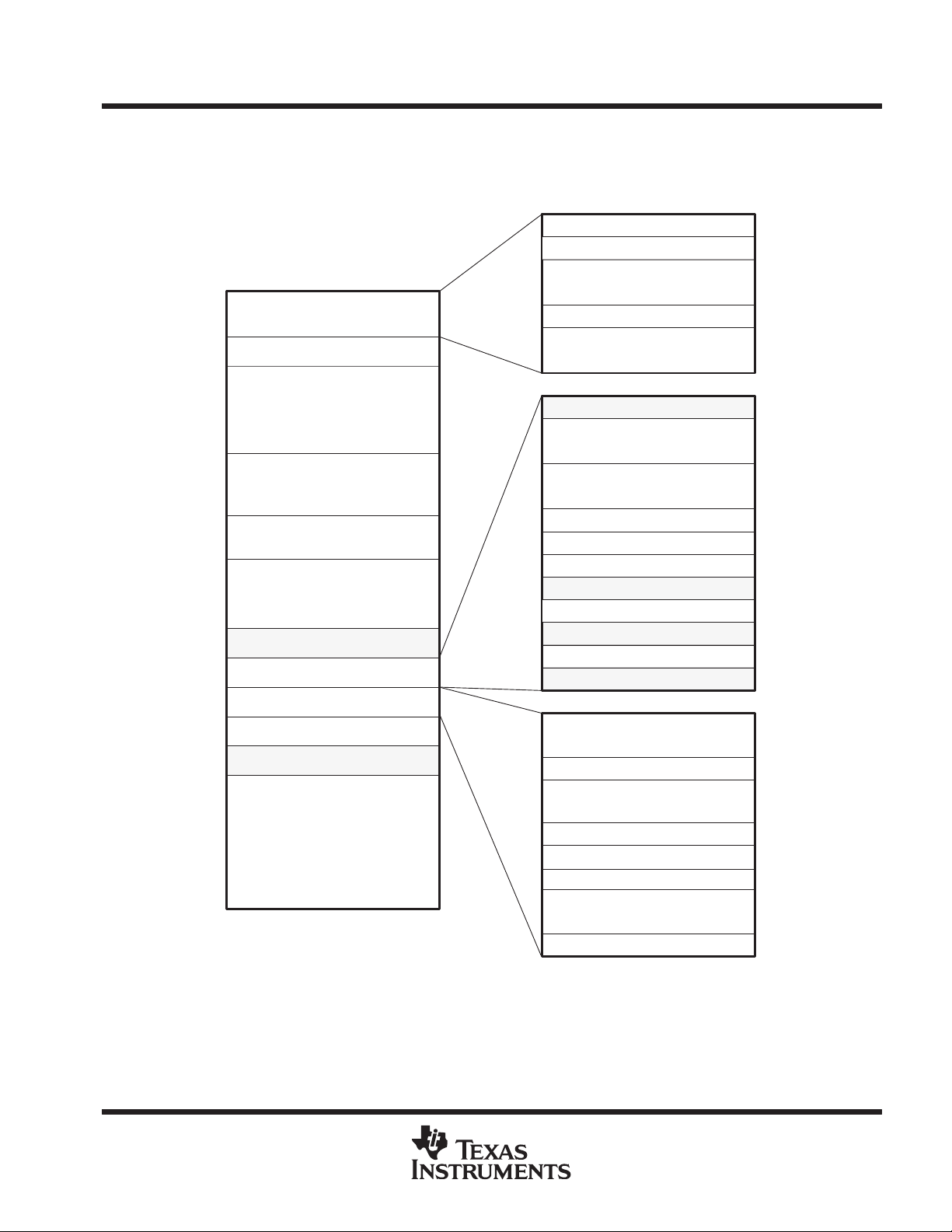
peripheral memory map
The TMS320x240 system and peripheral control register frame contains all the data, status, and control bits
to operate the system and peripheral modules on the device (excluding the event manager).
Hex
0000
0003
0004
0005
0006
0007
005F
Hex
0000
005F
0060
007F
0080
Memory-Mapped Registers
and Reserved
On-Chip DARAM B2
Reserved
Interrupt-Mask Register
Global-Memory Allocation
Register
Interrupt Flag Register
Emulation Registers
and Reserved
01FF
0200
02FF
0300
03FF
0400
07FF
0800
6FFF
7000
73FF
7400
743F
7440
77FF
7800
7FFF
8000
FFFF
Reserved
On-Chip DARAM
B0 (CNF = 0)
Reserved (CNF = 1)
On-Chip
DARAM B1
Reserved
Illegal
Peripheral Frame 1
Peripheral Frame 2
Reserved
Illegal
External
Illegal
System Configuration and
Control Registers
Watchdog Timer and
PLL Control Registers
ADC
SPI
SCI
Illegal
External-Interrupt Registers
Illegal
Digital-I/O Control Registers
Illegal
General-Purpose
Timer Registers
Reserved
Compare, PWM, and
Deadband Registers
Reserved
Capture & QEP Registers
Reserved
Interrupt Mask, Vector and
Flag Registers
Reserved
7000–700F
7010–701F
7020–702F
7030–703F
7040–704F
7050–705F
7060–706F
7070–707F
7080–708F
7090–709F
70A0–73FF
7400–740C
740D–7410
7411–741C
741D–741F
7420–7426
7427–742B
742C–7434
7435–743F
Figure 2. Peripheral Memory Map
POST OFFICE BOX 1443 • HOUSTON, TEXAS 77251–1443
15
TMS320C240, TMS320F240
DSP CONTROLLERS
SPRS042D – OCTOBER 1996 – REVISED NOVEMBER 1998
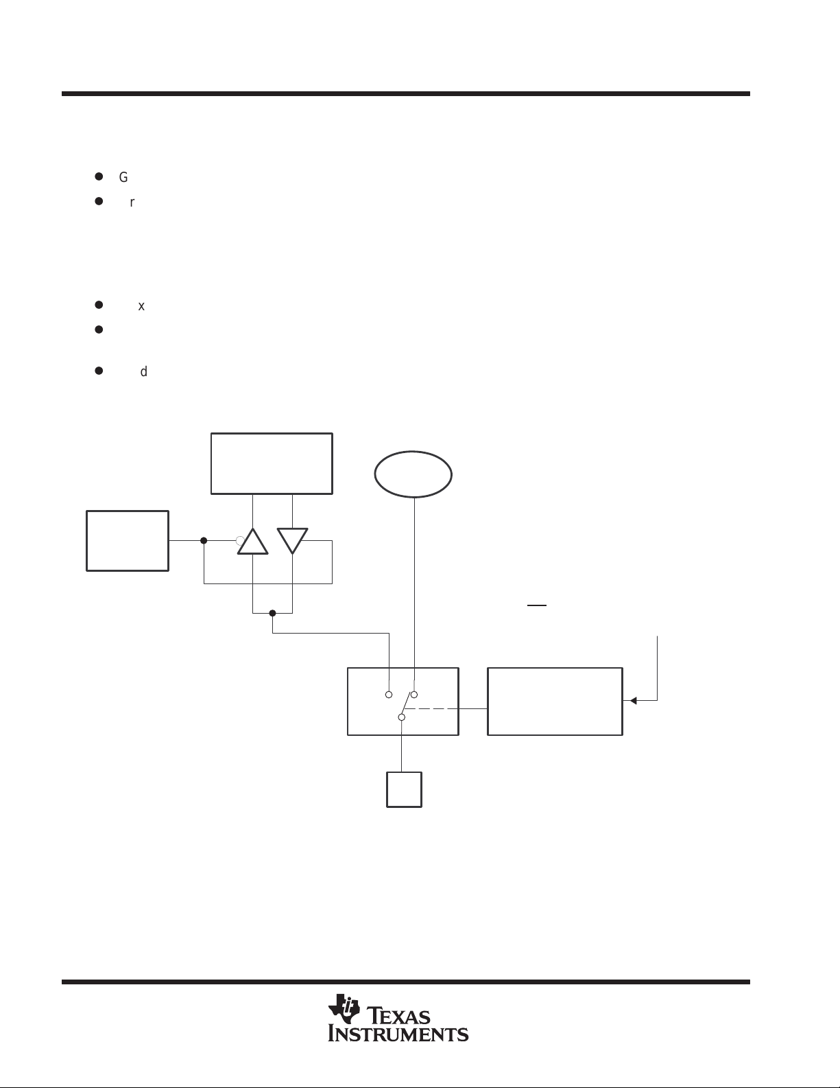
digital I/O and shared pin functions
The ’C240 has a total of 28 pins shared between primary functions and I/Os. These pins are divided into two
groups:
D
Group1 — Primary functions shared with I/Os belonging to dedicated I/O ports, Port A, Port B, and Port C.
D
Group2 — Primary functions belonging to peripheral modules which also have a built-in I/O feature as a
secondary function (for example, SCI, SPI, external interrupts, and PLL clock modules).
description of group1 shared I/O pins
The control structure for Group1 type shared I/O pins is shown in Figure 3. The only exception to this
configuration is the CLKOUT/IOPC1 pin. In Figure 3, each pin has three bits that define its operation:
D
Mux control bit — this bit selects between the primary function (1) and I/O function (0) of the pin.
D
I/O direction bit — if the I/O function is selected for the pin (mux control bit is set to 0), this bit determines
whether the pin is an input (0) or an output (1).
D
I/O data bit — if the I/O function is selected for the pin (mux control bit is set to 0) and the direction selected
is an input, data is read from this bit; if the direction selected is an output, data is written to this bit.
The mux control bit, I/O direction bit, and I/O data bit are in the I/O control registers.
IOP DIR Bit
0 = Input
1 = Output
IOP Data Bit
(Read/Write)
In Out
Figure 3. Shared Pin Configuration
Primary
Function
or I/O Pin
Primary
Function
01
Pin
Note:
When the MUX control bit = 1, the primary
function is selected in all cases except
for the following pins:
1. XF/IOPC2 (0 = Primary Function)
/IOPC3 (0 = Primary Function)
2. BIO
MUX Control Bit
0 = I/O Function
1 = Primary Function
A summary of Group1 pin configurations and associated bits is shown in Table 2.
16
POST OFFICE BOX 1443 • HOUSTON, TEXAS 77251–1443
PIN #
REGISTER
description of group1 shared I/O pins (continued)
Table 2. Group1 Shared Pin Configurations
TMS320C240, TMS320F240
DSP CONTROLLERS
SPRS042D – OCTOBER 1996 – REVISED NOVEMBER 1998
MUX CONTROL
(name.bit #)
72 OCRA.0 ADCIN0 IOPA0 PADATDIR 0 8
73 OCRA.1 ADCIN1 IOPA1 PADATDIR 1 9
90 OCRA.2 ADCIN9 IOPA2 PADATDIR 2 10
91 OCRA.3 ADCIN8 IOPA3 PADATDIR 3 11
100 OCRA.8 PWM7/CMP7 IOPB0 PBDATDIR 0 8
101 OCRA.9 PWM8/CMP8 IOPB1 PBDATDIR 1 9
102 OCRA.10 PWM9/CMP9 IOPB2 PBDATDIR 2 10
105 OCRA.11 T1PWM/T1CMP IOPB3 PBDATDIR 3 11
106 OCRA.12 T2PWM/T2CMP IOPB4 PBDATDIR 4 12
107 OCRA.13 T3PWM/T3CMP IOPB5 PBDATDIR 5 13
108 OCRA.14 TMRDIR IOPB6 PBDATDIR 6 14
109 OCRA.15 TMRCLK IOPB7 PBDATDIR 7 15
63 OCRB.0 ADCSOC IOPC0 PCDATDIR 0 8
64 SYSCR.7–6
0 0 IOPC1 PCDATDIR 1 9
0 1 WDCLK — — —
1 0 SYSCLK — — —
1 1 CPUCLK — — —
65 OCRB.2 IOPC2 XF PCDATDIR 2 10
66 OCRB.3 IOPC3 BIO PCDATDIR 3 11
67 OCRB.4 CAP1/QEP1 IOPC4 PCDATDIR 4 12
68 OCRB.5 CAP2/QEP2 IOPC5 PCDATDIR 5 13
69 OCRB.6 CAP3 IOPC6 PCDATDIR 6 14
70 OCRB.7 CAP4 IOPC7 PCDATDIR 7 15
†
Valid only if the I/O function is selected on the pin.
PIN FUNCTION SELECTED I/O PORT DATA AND DIRECTION
(CRx.n = 1) (CRx.n = 0) REGISTER DATA BIT # DIR BIT #
†
POST OFFICE BOX 1443 • HOUSTON, TEXAS 77251–1443
17
TMS320C240, TMS320F240
DSP CONTROLLERS
SPRS042D – OCTOBER 1996 – REVISED NOVEMBER 1998
description of group2 shared I/O pins
Group2 shared pins belong to peripherals that have built-in general-purpose I/O capability. Control and
configuration for these pins are achieved by setting the appropriate bits within the control and configuration
registers of the peripherals. Table 3 lists the Group2 shared pins.
Table 3. Group2 Shared Pin Configurations
PIN # PRIMARY FUNCTION REGISTER ADDRESS PERIPHERAL MODULE
43 SCIRXD SCIPC2 705Eh SCI
44 SCITXD SCIPC2 705Eh SCI
45 SPISIMO SPIPC2 704Eh SPI
48 SPISOMI SPIPC2 704Eh SPI
49 SPICLK SPIPC1 704Dh SPI
51 SPISTE SPIPC1 704Dh SPI
54 XINT2 XINT2CR 7078h External Interrupts
55 XINT3 XINT3CR 707Ah External Interrupts
digital I/O control registers
Table 4 lists the registers available to the digital I/O module. As with other ’x240 peripherals, the registers are
memory-mapped to the data space.
Table 4. Addresses of Digital I/O Control Registers
ADDRESS REGISTER NAME
7090h OCRA I/O mux control register A
7092h OCRB I/O mux control register B
7098h PADATDIR I/O port A data and direction register
709Ah PBDATDIR I/O port B data and direction register
709Ch PCDATDIR I/O port C data and direction register
device reset and interrupts
The TMS320x240 software-programmable interrupt structure supports flexible on-chip and external interrupt
configurations to meet real-time interrupt-driven application requirements. The ’x240 recognizes three types of
interrupt sources:
D
Reset (hardware- or software-initiated) is unarbitrated by the CPU and takes immediate priority over any
other executing functions. All maskable interrupts are disabled until the reset service routine enables them.
D
Hardware-generated interrupts are requested by external pins or by on-chip peripherals. There are two
types:
–
External interrupts
are generated by one of five external pins corresponding to the interrupts XINT1,
XINT2, XINT3, PDPINT , and NMI. The first four can be masked both by dedicated enable bits and by t he
CPU’ s interrup t mask regi ster (IMR ), which c an mask ea ch maskab le interr upt line a t the DSP cor e. NMI,
which is not maskable, takes priority over peripheral interrupts and software-generated interrupts. It can
be locked out only by an already executing NMI or a reset.
18
–
Peripheral interrupts
are initiated internally by these on-chip peripheral modules: the event manager,
SPI, SCI, watchdog/real-time interrupt (WD/RTI), and ADC. They can be masked both by enable bits
for each event in each peripheral and by the CPU’s IMR, which can mask each maskable interrupt line at
the DSP core.
POST OFFICE BOX 1443 • HOUSTON, TEXAS 77251–1443
device reset and interrupts (continued)
D
Software-generated interrupts for the ’x240 device include:
TMS320C240, TMS320F240
DSP CONTROLLERS
SPRS042D – OCTOBER 1996 – REVISED NOVEMBER 1998
The INTR instruction.
–
This instruction allows initialization of any ’x240 interrupt with software. Its
operand indicates to which interrupt vector location the CPU branches. This instruction globally
disables maskable interrupts (sets the INTM bit to 1).
–
The NMI instruction.
This instruction forces a branch to interrupt vector location 24h, the same location
used for the nonmaskable hardware interrupt NMI. NMI can be initiated by driving the NMI pin low or by
executing an NMI instruction. This instruction globally disables maskable interrupts.
–
The TRAP instruction.
TRAP instruction does
This instruction forces the CPU to branch to interrupt vector location 22h. The
not
disable maskable interrupts (INTM is not set to 1); therefore, when the CPU
branches to the interrupt service routine, that routine can be interrupted by the maskable hardware
interrupts.
–
An emulator trap.
This interrupt can be generated with either an INTR instruction or a TRAP instruction.
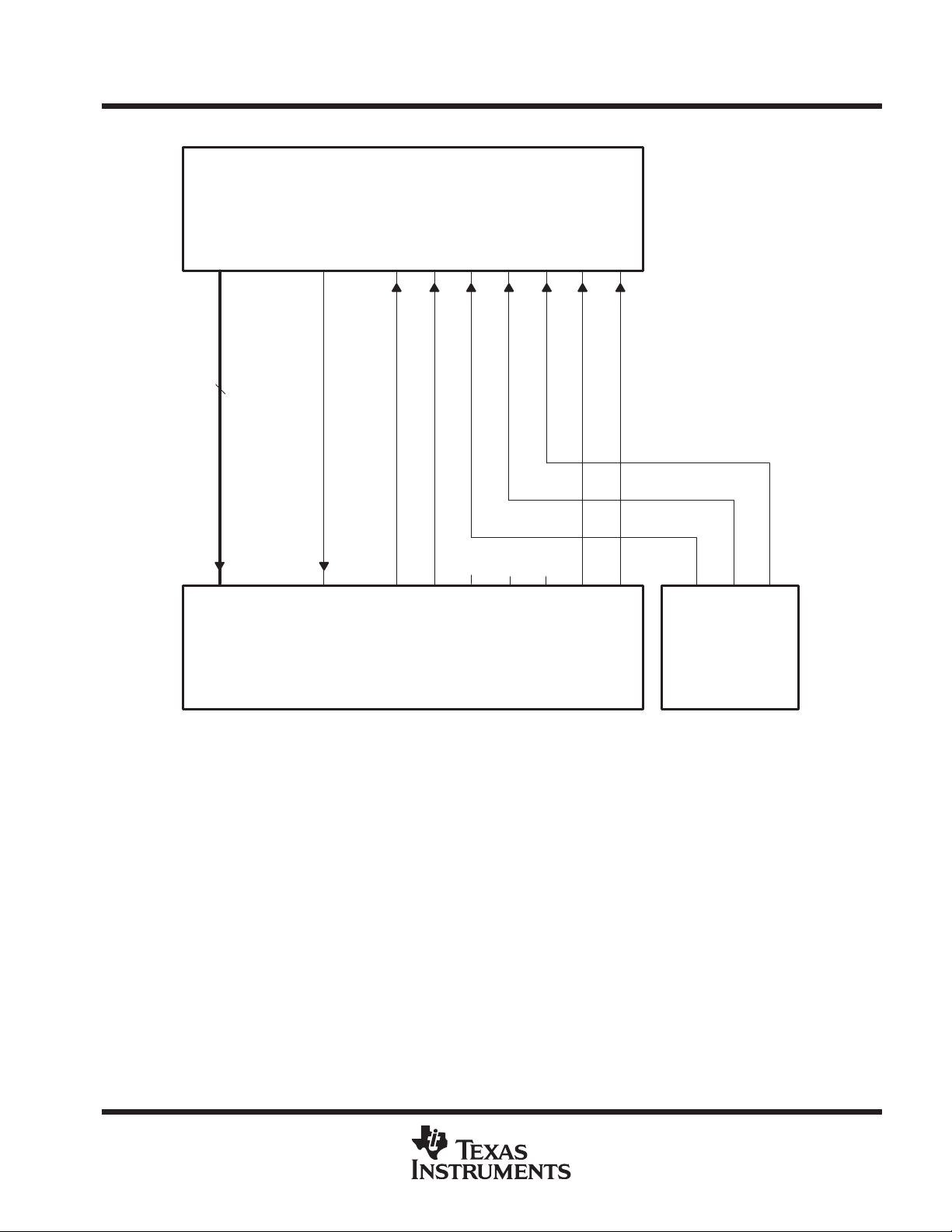
reset
The reset operation ensures an orderly startup sequence for the device. There are five possible causes of a
reset, as shown in Figure 4. Three of these causes are internally generated; the other two causes, the RS and
PORESET pins, are controlled externally.
To Device
Watchdog Timer Reset
Software-Generated Reset
Illegal Address Reset
Power-On Reset (PORESET
Reset (RS
) Pin Active
) Pin
Active
Reset
Signal
To Reset Out
Figure 4. Reset Signals
The five possible reset signals are generated as follows:
D
Watchdog timer reset. A watchdog-timer-generated reset occurs if the watchdog timer overflows or an
improper value is written to either the watchdog key register or the watchdog control register. (Note that
when the device is powered on, the watchdog timer is automatically active.)
D
Software-generated reset. This is implemented with the system control register (SYSCR). Clearing the
RESET0 bit (bit 14) or setting the RESET1 bit (bit 15) causes a system reset.
D
Illegal address reset. The system and peripheral module control register frame address map contains
unimplemented address locations in the ranges labeled illegal. Any access to an address located in the
Illegal ranges generate an illegal-address reset.
D
Reset pin active. To generate an external reset pulse on the RS pin, a low-level pulse duration of as little
as a few nanoseconds is usually effective; however , pulses of one SYSCLK cycle are necessary to ensure
that the device recognizes the reset signal.
D
Power-on reset pin active. To generate a power-on reset pulse on the PORESET pin, a low-level pulse
of one SYSCLK cycle is necessary to ensure that the device recognizes the reset signal.
Once a reset source is activated, the external RS
pin is driven (active) low for a minimum of eight SYSCLK
cycles. This allows the TMS320x240 device to reset external system components. Additionally , if a brown-out
condition (VCC < VCCmin for several microseconds causing PORESET to go low) occurs or the RS pin is held
low, then the reset logic holds the device in a reset state for as long as these actions are active.
POST OFFICE BOX 1443 • HOUSTON, TEXAS 77251–1443
19
TMS320C240, TMS320F240
DSP CONTROLLERS
SPRS042D – OCTOBER 1996 – REVISED NOVEMBER 1998
reset (continued)
The occurrence of a reset condition causes the TMS320x240 to terminate program execution and affects
various registers and status bits. During a reset, RAM contents remain unchanged, and all control bits that are
affected by a reset are initialized to their reset state. In the case of a power-on reset, the PLL control registers
are initialized to zero. The program needs to recognize power-on resets and configure the PLL for correct
operation.
After a reset, the program can check the power-on reset flag (PORST flag, SYSSR.15), the illegal address flag
(ILLADR flag, SYSSR.12), the software reset flag (SWRST flag, SYSSR.10), and the watchdog reset flag
(WDRST flag, SYSSR.9) to determine the source of the reset. A reset does not clear these flags.
RS
and PORESET must be held low until the clock signal is valid and VCC is within the operating range. In
addition, PORESET must be driven low when VCC drops below the minimum operating voltage.
hardware-generated interrupts
All the hardware interrupt lines of the DSP core are given a priority rank from 1 to 10 (1 being highest). When
more than one of these hardware interrupts is pending acknowledgment, the interrupt of highest rank gets
acknowledged first. The others are acknowledged in order after that. Of those ten lines, six are for maskable
interrupt lines (INT1–INT6) and one is for the nonmaskable interrupt (NMI) line. INT1–INT6 and NMI have the
priorities shown in Table 5.
Table 5. Interrupt Priorities at the Level of the DSP Core
INTERRUPT
RESET 1
TI RESERVED
NMI 3
INT1 4
INT2 5
INT3 6
INT4 7
INT5 8
INT6 9
TI RESERVED
†
TI Reserved means that the address space is
reserved for Texas Instruments.
†
†
PRIORITY AT THE
DSP CORE
2
10
The inputs to these lines are controlled by the system module and the event manager as summarized in T able 6
and shown in Figure 5.
Table 6. Interrupt Lines Controlled by the System Module and Event Manager
PERIPHERAL INTERRUPT LINES
INT1
System Module
Event Manager
INT5
INT6
INT2
INT3
INT4
NMI
20
POST OFFICE BOX 1443 • HOUSTON, TEXAS 77251–1443
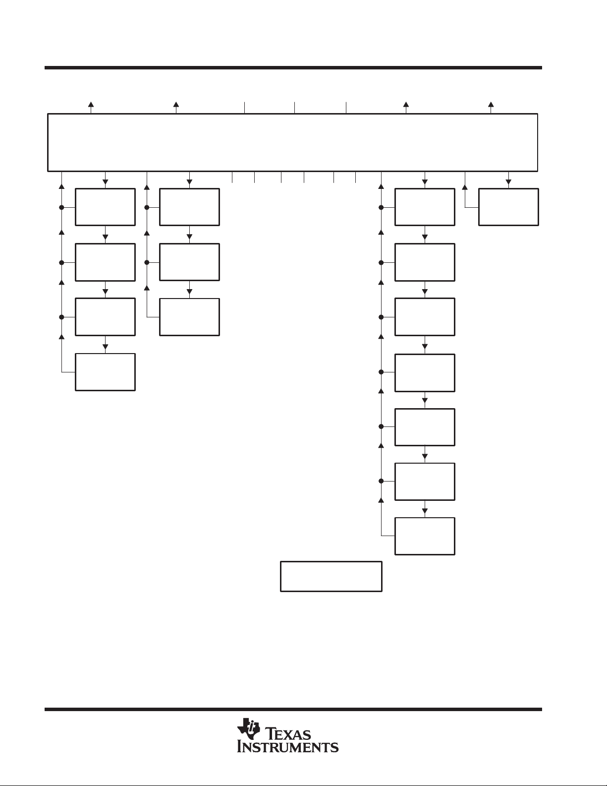
hardware-generated interrupts (continued)
DSP Core
TMS320C240, TMS320F240
DSP CONTROLLERS
SPRS042D – OCTOBER 1996 – REVISED NOVEMBER 1998
Address
Lines 5–1
5
Address
Lines 5–1
IACK
INT6 INT5 INT4 INT3 INT2 INT1 NMI
NC NC NC
INT6 INT5 INT4 INT3 INT2 INT1 NMIIACK
System Module Event Manager
INTC INTB INTA
Figure 5. DSP Interrupt Structure
At the level of the system module and the event manager, each of the maskable interrupt lines (INT1–INT6) is
connected to multiple maskable interrupt sources. Sources connected to interrupt line INT1 are called Level 1
interrupts; sources connected to interrupt line INT2 are called Level 2 interrupts; and so on. For each interrupt
line, the multiple sources also have a set priority ranking. The source with the highest priority has its interrupt
request responded to by the DSP core first.
Figure 6 shows the sources and priority ranking for the interrupts controlled by the system module. For each
interrupt chain, the interrupt source of highest priority is at the top. Priority decreases from the top of the chain
to the bottom. Figure 7 shows the interrupt sources and priority ranking for the event manager interrupts.
POST OFFICE BOX 1443 • HOUSTON, TEXAS 77251–1443
21
TMS320C240, TMS320F240
DSP CONTROLLERS
SPRS042D – OCTOBER 1996 – REVISED NOVEMBER 1998
hardware-generated interrupts (continued)
To DSP INT6 To DSP INT1 To DSP NMI
To DSP INT5
NCNCNC
Dual ADC
Interrupt
System-Module
External Interrupt
XINT1
(low priority)
System-Module
External Interrupt
XINT2
(low priority)
System-Module
External Interrupt
XINT3
(low priority)
INT5
SPI
Interrupt
(low priority)
SCI
Receiver
Interrupt
(low priority)
SCI
Transmitter
Interrupt
(low priority)
System Module
INT2INT3INT4
IACK1IRQ1IACK5IRQ5IACK6IRQ6
NCNCNCNCNCNC
System-Module
External Interrupt
XINT1
(high priority)
System-Module
External Interrupt
XINT2
(high priority)
System-Module
External Interrupt
XINT3
(high priority)
Watchdog
Timer
Interrupt
NMIINT1INT6
IACK_NMIIRQ_NMIIACK2IRQ2IACK3IRQ3IACK4IRQ4
System-Module
External Interrupt
NMI
Legend:
NC = No connection
IACK = interrupt acknowledge
IRQ = interrupt request
Figure 6. System-Module Interrupt Structure
SPI
Interrupt
(high priority)
SCI
Receiver
Interrupt
(high priority)
SCI
Transmitter
Interrupt
(high priority)
22
POST OFFICE BOX 1443 • HOUSTON, TEXAS 77251–1443
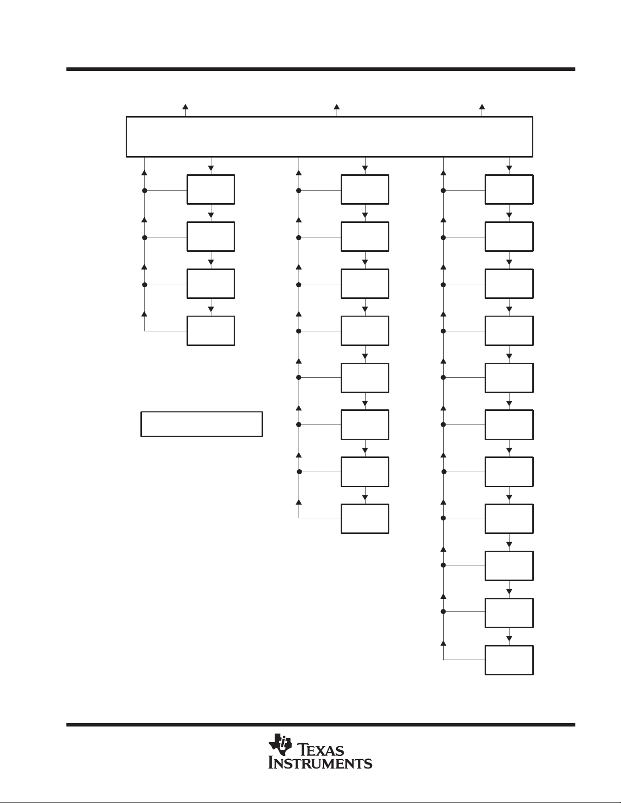
hardware-generated interrupts (continued)
To DSP INT4 To DSP INT3 To DSP INT2
TMS320C240, TMS320F240
DSP CONTROLLERS
SPRS042D – OCTOBER 1996 – REVISED NOVEMBER 1998
INTAINTBINTC
Event Manager
IACKAIRQAIACKBIRQBIACKCIRQC
Legend:
Capture 1
Interrupt
Capture 2
Interrupt
Capture 3
Interrupt
Capture 4
Interrupt
IACK = Interrupt acknowledge
IRQ = Interrupt request
Timer 2
Period
Interrupt
Timer 2
Compare
Interrupt
Timer 2
Underflow
Interrupt
Timer 2
Overflow
Interrupt
Timer 3
Period
Interrupt
Timer 3
Compare
Interrupt
Timer 3
Underflow
Interrupt
Power-Drive
Protection
Interrupt
Compare1
Interrupt
Compare 2
Interrupt
Compare 3
Interrupt
Simple-
Compare 1
Interrupt
Simple-
Compare 2
Interrupt
Simple-
Compare 3
Interrupt
Timer 3
Overflow
Interrupt
Figure 7. Event-Manager Interrupt Structure
POST OFFICE BOX 1443 • HOUSTON, TEXAS 77251–1443
Timer 1
Period
Interrupt
Timer 1
Compare
Interrupt
Timer 1
Underflow
Interrupt
Timer 1
Overflow
Interrupt
23

TMS320C240, TMS320F240
DSP CONTROLLERS
SPRS042D – OCTOBER 1996 – REVISED NOVEMBER 1998
hardware-generated interrupts (continued)
Each of the interrupt sources has its own control register with a flag bit and an enable bit. When an interrupt
request is received, the flag bit in the corresponding control register is set. If the enable bit is also set, a signal
is sent to arbitration logic, which can simultaneously receive similar signals from one or more of the other control
registers. The arbitration logic compares the priority level of competing interrupt requests, and it passes the
interrupt of highest priority to the CPU. The corresponding flag is set in the interrupt flag register (IFR), indicating
that the interrupt is pending. The CPU then must decide whether to acknowledge the request. Maskable
hardware interrupts are acknowledged only after certain conditions are met:
D
Priority is highest. When more than one hardware interrupt is requested at the same time, the ’x240
services them according to the set priority ranking.
D
INTM bit is 0. The interrupt mode (INTM) bit, bit 9 of status register ST0, enables or disables all maskable
interrupts:
– When INTM = 0, all unmasked interrupts are enabled.
– When INTM = 1, all unmasked interrupts are disabled.
INTM is set to 1 automatically when the CPU acknowledges an interrupt (except when initiated by the TRAP
instruction) and at reset. It can be set and cleared by software.
D
IMR mask bit is 1. Each of the maskable interrupt lines has a mask bit in the interrupt mask register (IMR).
To unmask an interrupt line, set its IMR bit to 1.
When the CPU acknowledges a maskable hardware interrupt, it jams the instruction bus with the INTR
instruction. This instruction forces the PC to the appropriate address from which the CPU fetches the software
vector. This vector leads to an interrupt service routine.
Usually, the interrupt service routine reads the peripheral-vector-address offset from the peripheral-vectoraddress register (see Table 7) to branch to code that is meant for the specific interrupt source that initiated the
interrupt request. The ’x240 includes a phantom-interrupt vector offset (0000h), which is a system interrupt
integrity feature that allows a controlled exit from an improper interrupt sequence. If the CPU acknowledges a
request from a peripheral when, in fact, no peripheral has requested an interrupt, the phantom-interrupt vector
is read from the interrupt-vector register.
Table 7 summarizes the interrupt sources, overall priority, vector address/offset, source, and function of each
interrupt available on the TMS320x240.
24
POST OFFICE BOX 1443 • HOUSTON, TEXAS 77251–1443
(System)
0004h
0006h
M
Grou B)
M
hardware-generated interrupts (continued)
Table 7. ’x240 Interrupt Locations and Priorities
TMS320C240, TMS320F240
DSP CONTROLLERS
SPRS042D – OCTOBER 1996 – REVISED NOVEMBER 1998
INTERRUPT
NAME
RS
RESERVED 2
NMI 3
XINT1
XINT2
XINT3
SPIINT 7
RXINT 8
TXINT 9
WDTINT 10 0010h Y WDT Watchdog timer interrupt
PDPINT 11 0020h Y External Power-drive protection Int.
CMP1INT 12 0021h Y EV.CMP1 Full Compare 1 interrupt
CMP2INT 13 0022h Y EV.CMP2 Full Compare 2 interrupt
CMP3INT 14 0023h Y EV.CMP3 Full Compare 3 interrupt
SCMP1INT 15
SCMP2INT 16
SCMP3INT 17
TPINT1 18 0027h Y EV.GPT1 Timer1-period interrupt
TCINT1 19 0028h Y EV.GPT1 Timer1-compare interrupt
TUFINT1 20 0029h Y EV.GPT1 Timer1-underflow interrupt
TOFINT1 21 002Ah Y EV.GPT1 T imer1-overflow interrupt
TPINT2 22 002Bh Y EV.GPT2 T imer2-period interrupt
TCINT2 23
TUFINT2 24
TOFINT2 25
TPINT3 26
TCINT3 27
TUFINT3 28
TOFINT3 29 0032h Y EV.GPT3 Timer3-overflow interrupt
CAPINT1 30 INT4 0033h Y EV.CAP1 Capture 1 interrupt
CAPINT2 31 0008h
CAPINT3 32
CAPINT4 33
OVERALL
PRIORITY
1
Highest
4
5
6
DSP-CORE
INTERRUPT,
AND
ADDRESS
RS
0000h
INT7
0026h
NMI
0024h
INT1
0002h
INT2
(Event
Manager
Group A)
INT3
(Event
anager
p
(Event
anager
Group C)
PERIPHERAL
VECTOR
ADDRESS
N/A N Core, SD
N/A N/A N DSP Core Emulator trap
N/A 0002h N Core, SD External user interrupt
SYSIVR
(701Eh)
EVIVRA
(7432h)
EVIVRB
(7433h)
EVIVRC
(7434h)
PERIPHERAL
VECTOR
ADDRESS
OFFSET
0001h
0011h
001Fh
0005h Y SPI High-priority SPI interrupt
0006h Y SCI
0007h Y SCI
0024h Y EV.CMP4
0025h Y EV.CMP5
0026h Y EV.CMP6
002Ch Y EV.GPT2 Timer2-compare interrupt
002Dh Y EV.GPT2 Timer2-underflow interrupt
002Eh Y EV.GPT2 T imer2-overflow interrupt
002Fh Y EV.GPT3 Timer3-period interrupt
0030h Y EV.GPT3 Timer3-compare interrupt
0031h Y EV.GPT3 Timer3-underflow interrupt
0034h Y EV.CAP2 Capture 2 interrupt
0035h Y EV.CAP3 Capture 3 interrupt
0036h Y EV.CAP4 Capture 4 interrupt
MASKABLE?
Y SD
’x240
SOURCE
PERIPHERAL
MODULE
FUNCTION
INTERRUPT
External, system reset
(RESET)
High-priority external user
interrupts
SCI receiver interrupt
(high priority)
SCI transmitter interrupt
(high priority)
Simple compare 1
interrupt
Simple compare 2
interrupt
Simple compare 3
interrupt
POST OFFICE BOX 1443 • HOUSTON, TEXAS 77251–1443
25
TMS320C240, TMS320F240
SYSIVR
XINT2
39
(701Eh)
0011h
Y
y
DSP CONTROLLERS
SPRS042D – OCTOBER 1996 – REVISED NOVEMBER 1998
hardware-generated interrupts (continued)
Table 7. ’x240 Interrupt Locations and Priorities (Continued)
INTERRUPT
NAME
SPIINT 34 INT5
RXINT 35
TXINT 36
ADCINT 37 INT6 SYSIVR 0004h Y ADC Analog-to-digital interrupt
XINT1
XINT3
RESERVED 41 000Eh N/A Y DSP Core Used for analysis
TRAP N/A 0022h N/A N/A TRAP instruction vector
OVERALL
PRIORITY
38
40
DSP-CORE
INTERRUPT,
AND
ADDRESS
000Ah
(System)
000Ch
(System)
PERIPHERAL
VECTOR
ADDRESS
(701Eh)
PERIPHERAL
VECTOR
ADDRESS
OFFSET
0005h Y SPI Low-priority SPI interrupt
0006h Y SCI
0007h Y SCI
0001h
001Fh
MASKABLE?
Y
Y
’x240
SOURCE
PERIPHERAL
MODULE
External Low-priority external
pins
FUNCTION
INTERRUPT
SCI receiver interrupt
(low priority)
SCI transmitter interrupt
(low priority)
user interrupts
external interrupts
The ’x240 has five external interrupts. These interrupts include:
D
XINT1. Type A interrupt. The XINT1 control register (at 7070h) provides control and status for this interrupt.
XINT1 can be used as a high-priority (Level 1) or low-priority (Level 6) maskable interrupt or as a
general-purpose input pin. XINT1 can also be programmed to trigger an interrupt on either the rising or the
falling edge.
D
NMI. T ype A inter rupt. The NMI control register (at 7072h) provides control and status for this interrupt. NMI
is a nonmaskable external interrupt or a general-purpose input pin. NMI can also be programmed to trigger
an interrupt on either the rising or the falling edge.
D
XINT2. Type C interrupt. The XINT2 control register (at 7078h) provides control and status for this interrupt.
XINT2 can be used as a high-priority (Level 1) or low-priority (Level 6) maskable interrupt or a
general-purpose I/O pin. XINT2 can also be programmed to trigger an interrupt on either the rising or the
falling edge.
D
XINT3. Type C interrupt. The XINT3 control register (at 707Ah) provides control and status for this interrupt.
XINT3 can be used as a high-priority (Level 1) or low-priority (Level 6) maskable interrupt or as a
general-purpose I/O pin. XINT3 can also be programmed to trigger an interrupt on either the rising or the
falling edge.
D
PDPINT. This interrupt is provided for safe operation of the power converter and motor drive. This maskable
interrupt can put the timers and PWM output pins in the high-impedance state and inform the CPU in case
of motor drive abnormalities such as overvoltage, overcurrent, and excessive temperature rise. PDP IN T is
a Level 2 interrupt.
26
POST OFFICE BOX 1443 • HOUSTON, TEXAS 77251–1443
external interrupts (continued)
Table 8 is a summary of the external interrupt capability of the ’x240.
Table 8. External Interrupt Types and Functions
TMS320C240, TMS320F240
DSP CONTROLLERS
SPRS042D – OCTOBER 1996 – REVISED NOVEMBER 1998
EXTERNAL
INTERRUPT
XINT1 XINT1CR 7070h A No Input only
NMI NMICR 7072h A Yes Input only No
XINT2 XINT2CR 7078h C No I/O
XINT3 XINT3CR 707Ah C No I/O
PDPINT EVIMRA 742Ch N/A N/A N/A
CONTROL
REGISTER
NAME
CONTROL
REGISTER
ADDRESS
INTERRUPT
TYPE
CAN DO
NMI?
DIGITAL
I/O PIN
MASKABLE?
(Level 1 or 6)
(Level 1 or 6)
(Level 1 or 6)
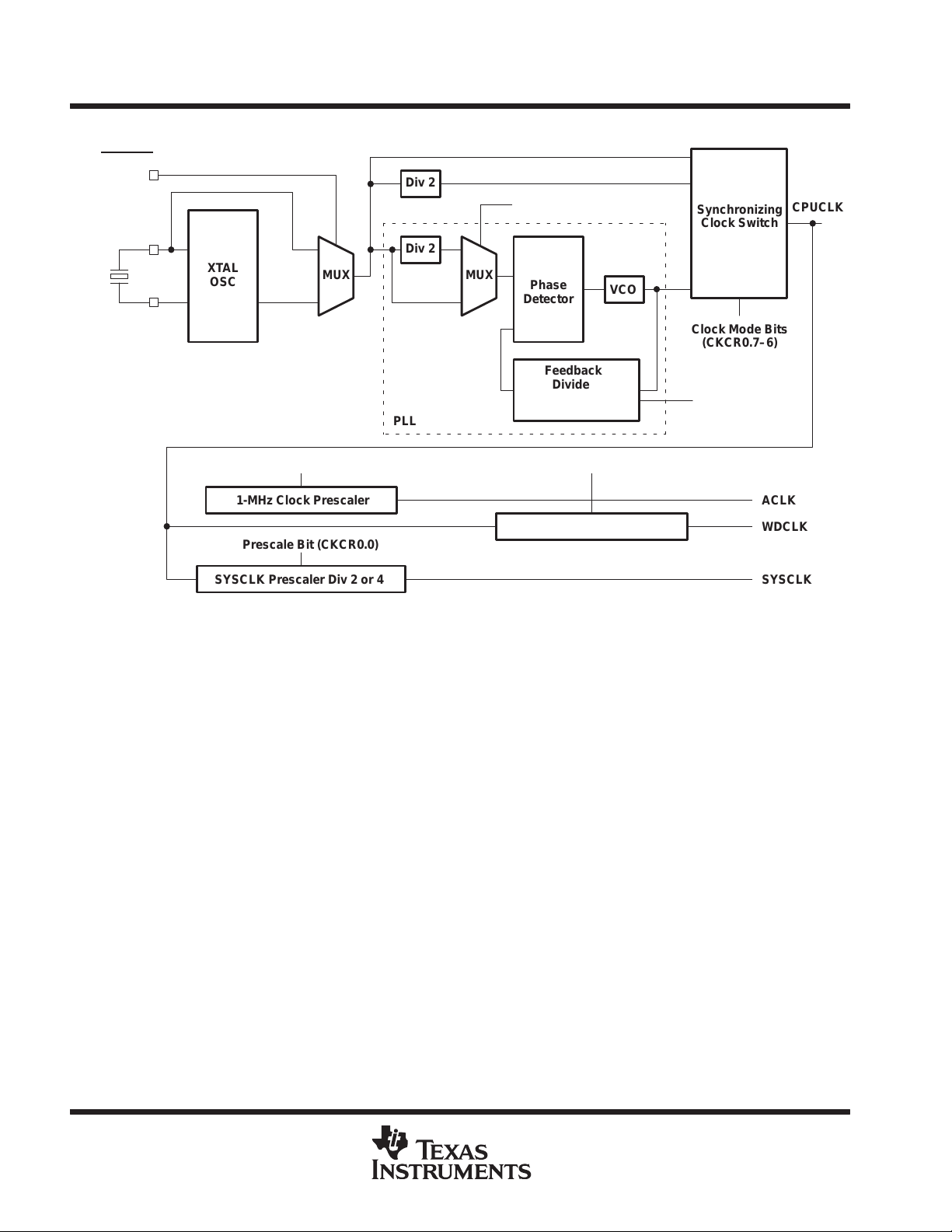
clock generation
The TMS320x240 has an on-chip, PLL-based clock module. This module provides all the necessary clocking
signals for the device, as well as control for low-power mode entry . The only external component necessary for
this module is an external fundamental crystal, or oscillator.
The PLL-based clock module provides two basic modes of operation: oscillator mode and clock-in mode.
D
oscillator mode
This mode allows the use of a 4-, 6-, or 8-MHz external reference crystal to provide the time base to the
device. The internal oscillator circuitry is initialized by software to select the desired CPUCLK frequency,
which can be the input clock frequency , the input clock frequency divided by 2 (default), or a clock frequency
determined by the PLL.
Yes
Yes
Yes
Yes
(Level 2)
D
Clock-in mode
This mode allows the internal crystal oscillator circuitry to be bypassed. The device clocks are generated
from an external clock source input on the XTAL1/CLKIN pin. The device can be configured by software
to operate on the input clock frequency, the input clock frequency divided by 2, or a clock frequency
determined by the PLL.
The ’x240 runs on two clock frequencies: the CPU clock (CPUCLK) frequency , and the system clock (SYSCLK)
frequency . The CPU, memories, external memory interface, and event manager run at the CPUCLK frequency .
All other peripherals run at the SYSCLK frequency . The CPUCLK runs at 2x or 4x the frequency of the SYSCLK;
for example, for 2x, CPUCLK = 20 MHz and SYSCLK = 10 MHz. There is also a clock for the watchdog timer,
WDCLK. This clock has a nominal frequency of 16384 Hz (214 Hz) when XTAL1/CLKIN is a power of two or
a sum of two powers of two; for example, 4194304 Hz (222 Hz), 6291456 (222 + 221 Hz), or 8388608 Hz
(223 Hz).
The clock module includes three external pins:
1. XTAL1/CLKIN clock source/crystal input
2. XTAL2 output to crystal
3. OSCBYP oscillator bypass
For the external pins, if OSCBYP ≥ VIH, then the oscillator is enabled and if OSCBYP ≤ VIL, then the oscillator
is bypassed and the device is in clock-in mode. In clock-in mode, an external TTL clock must be applied to the
XTAL1/CLKIN pin. The XTAL2 pin can be left unconnected.
POST OFFICE BOX 1443 • HOUSTON, TEXAS 77251–1443
27
TMS320C240, TMS320F240
DSP CONTROLLERS
SPRS042D – OCTOBER 1996 – REVISED NOVEMBER 1998
clock generation (continued)
OSCBYP
XTAL1/CLKIN
XTAL
OSC
XTAL2
Clock Frequency and PLL Multiply Bits (CKCR1.7–4)
PLL
Div 2
Div 2
PLL divide-by-2 bit
(CKCR1.3)
MUXMUX
Phase
Detector
Feedback
Divider
Div 1, 2, 3, 4, 5,
or 9
VCO
Synchronizing
Clock Switch
Clock Mode Bits
(CKCR0.7–6)
PLL multiply ratio
(CKCR1.2–0)
CPUCLK
1-MHz Clock Prescaler
Prescale Bit (CKCR0.0)
SYSCLK Prescaler Div 2 or 4
Figure 8. PLL Clock Module Block Diagram
Watchdog Clock Prescaler
ACLK
WDCLK
SYSCLK
28
POST OFFICE BOX 1443 • HOUSTON, TEXAS 77251–1443
TMS320C240, TMS320F240
DSP CONTROLLERS
SPRS042D – OCTOBER 1996 – REVISED NOVEMBER 1998
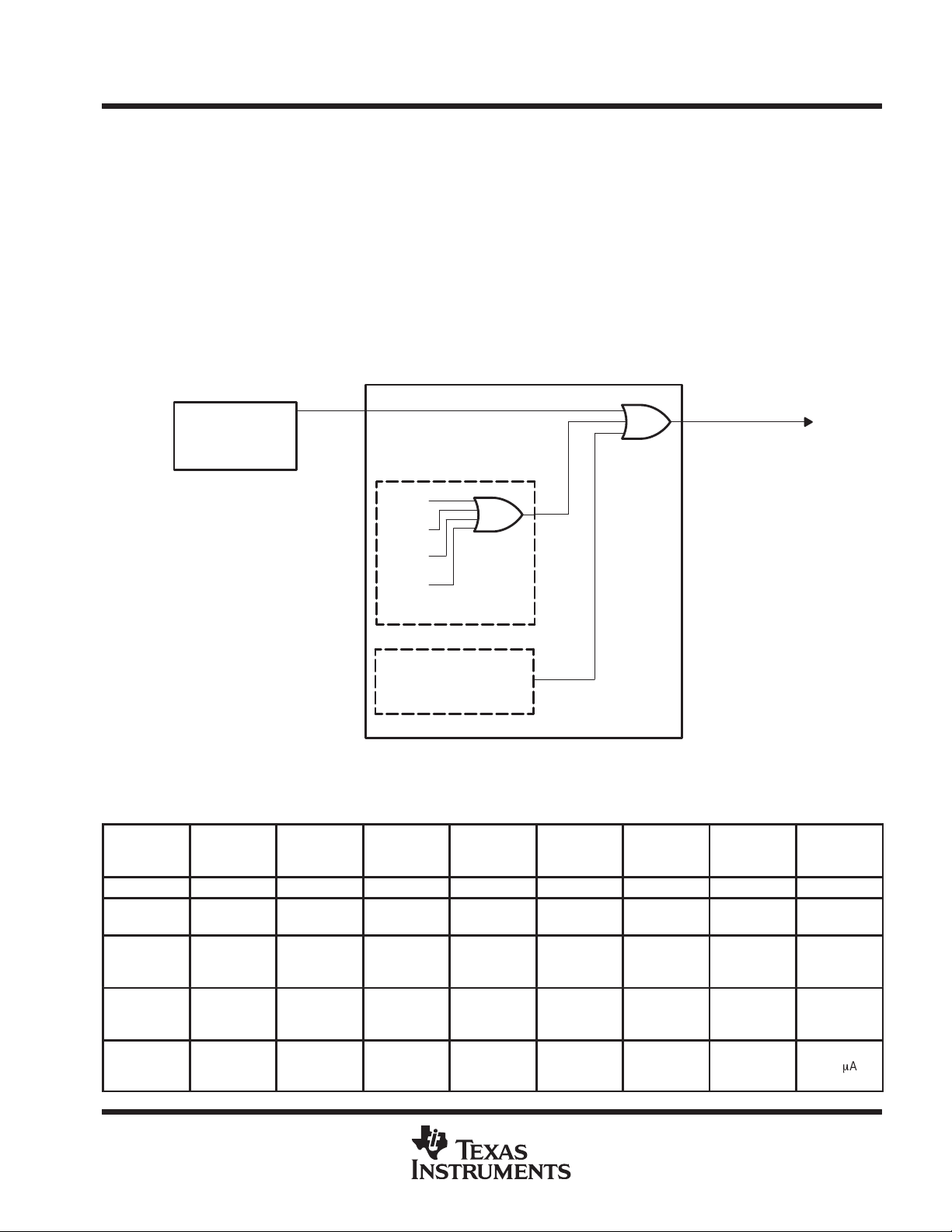
low-power modes
The TMS320x240 has four low-power modes (idle 1, idle 2, PLL power down, and oscillator power down). The
low-power modes reduce the operating power by reducing or stopping the activity of various modules (by
stopping their clocks). The two PLLPM bits of the clock module control register, CKCR0, select which of the
low-power modes the device enters when executing an IDLE instruction. Reset or an unmasked interrupt from
any source causes the device to exit from idle 1 low-power mode. A real-time interrupt from the watchdog timer
module causes the device to exit from all low-power modes except oscillator power down. This is a wake-up
interrupt. When enabled, reset or any of the four external interrupts (NMI, XINT1, XINT2, or XINT3) causes the
device to exit from any of the low-power modes (idle 1, idle 2, PLL power down, and oscillator power down).
The external interrupts are all wake-up interrupts. The maskable external interrupts (XINT1, XINT2, and XINT3)
must be enabled individually and globally to bring the device out of a low-power mode properly . It is, therefore,
important to ensure that the desired low-power-mode exit path is enabled before entering a low-power mode.
Figure 9 shows the wake-up sequence from a power down. Table 9 summarizes the low-power modes.
Watchdog Timer
and
Real-Time Interrupt
Module
Wake-up
Signal
Wake-up Signal
to CPU
NMI
XINT1
XINT2
XINT3
External-Interrupt Logic
Reset
Signal
Reset Logic
System Module
Figure 9. Waking Up the Device From Power Down
Table 9. Low-Power Modes
LOW-
POWER
MODE
Run XX On On On On On – 80 mA
Idle 1 00 Off On On On On
Idle 2 01 Off Off On On On
PLL Power
Down
OSC Power
Down
PLLPM(x)
BITS IN
CKCR0[2:3]
10 Off Off On Off On
11 Off Off Off Off Off
CPUCLK
STATUS
SYSCLK
STATUS
WDCLK
STATUS
PLL
STATUS
OSC
STATUS
EXIT
CONDITION
Any interrupt
or reset
Wake-up
interrupt or
reset
Wake-up
interrupt or
reset
Wake-up
interrupt or
reset
TYPICAL
POWER
50 mA
7 mA
1 mA
400 mA
POST OFFICE BOX 1443 • HOUSTON, TEXAS 77251–1443
29
TMS320C240, TMS320F240
DSP CONTROLLERS
SPRS042D – OCTOBER 1996 – REVISED NOVEMBER 1998
functional block diagram of the TMS320x240 DSP CPU
IS
DS
PS
Control
MUXMUX
ARP(3)
ARB(3)
X1
CLKOUT1
CLKIN/X2
16
PC
W/R
WE
NMI
FLASH EEPROM/
16
1616
MUX
Data/Prog
DARAM
MUX
16
ROM
16
16
AR0(16)
AR1(16)
AR2(16)
AR3(16)
AR4(16)
AR5(16)
AR6(16)
AR7(16)
ARAU(16)
16
16
3
3
3
B0 (256 × 16)
A15–A0
D15–D0
R/W
STRB
READY
MP/MC
XINT[1–3]
16
BR
XF
RS
Data Bus
Memory Map
GREG (16)
3
16
16
3
Register
IMR (16)
IFR (16)
MUX
NPAR
PAR MSTACK
DP(9)
16
MUX
MUX
Data
DARAM
B2 (32 × 16)
B1 (256 × 16)
16
Program Bus
9
9
16
MUX
Stack 8 × 16
16
7
LSB
from
IR
MUX
ISCALE (0–16)
32
16
Program Control
(PCTRL)
16
16
16
16
PSCALE (–6, 0,1,4)
CALU(32)
ACCL(16)ACCH(16)C
OSCALE (0–7)
Data Bus
TREG0(16)
Multiplier
PREG(32)
32
3232
MUX
32
32
32
16
MUX
Data Bus
1616
16
Program Bus
Program Bus
NOTES: A. Symbol descriptions appear in Table 10.
B. For clarity the data and program buses are shown as single buses although they include address and data bits.
30
POST OFFICE BOX 1443 • HOUSTON, TEXAS 77251–1443

SPRS042D – OCTOBER 1996 – REVISED NOVEMBER 1998
TMS320C240, TMS320F240
Table 10. Legend for the ’F240 Internal Hardware Functional Block Diagram
SYMBOL NAME DESCRIPTION
ACC Accumulator
ARAU
AUX
REGS
BR
C Carry
CALU
DARAM Dual Access RAM
DP
GREG
IMR
IFR
INT# Interrupt Traps A total of 32 interrupts by way of hardware and/or software are available.
ISCALE
MPY Multiplier
MSTACK Micro Stack
MUX Multiplexer Multiplexes buses to a common input
NPAR
OSCALE
PAR
PC Program Counter
PCTRL
Auxiliary Register
Arithmetic Unit
Auxiliary Registers
0–7
Bus Request
Signal
Central Arithmetic
Logic Unit
Data Memory
Page Pointer
Global Memory
Allocation
Register
Interrupt Mask
Register
Interrupt Flag
Register
Input Data-Scaling
Shifter
Next Program
Address Register
Output
Data-Scaling
Shifter
Program Address
Register
Program
Controller
32-bit register that stores the results and provides input for subsequent CALU operations. Also includes shift
and rotate capabilities
An unsigned, 16-bit arithmetic unit used to calculate indirect addresses using the auxiliary registers as inputs
and outputs
These 16-bit registers are used as pointers to anywhere within the data space address range. They are
operated upon by the ARAU and are selected by the auxiliary register pointer (ARP). AR0 can also be used
as an index value for AR updates of more than one and as a compare value to AR.
BR is asserted during access of the external global data memory space. READY is asserted to the device
when the global data memory is available for the bus transaction. BR
address space by up to 32K words.
Register carry output from CALU. C is fed back into the CALU for extended arithmetic operation. The C bit
resides in status register 1 (ST1), and can be tested in conditional instructions. C is also used in accumulator
shifts and rotates.
32-bit-wide main arithmetic logic unit for the TMS320C2xx core. The CALU executes 32-bit operations in a
single machine cycle. CALU operates on data coming from ISCALE or PSCALE with data from ACC, and
provides status results to PCTRL.
If the on-chip RAM configuration control bit (CNF) is set to 0, the reconfigurable data dual-access RAM
(DARAM) block B0 is mapped to data space; otherwise, B0 is mapped to program space. Blocks B1 and B2
are mapped to data memory space only, at addresses 0300–03FF and 0060–007F, respectively. Blocks 0
and 1 contain 256 words, while Block 2 contains 32 words.
The 9-bit DP register is concatenated with the seven LSBs of an instruction word to form a direct memory
address of 16 bits. DP can be modified by the LST and LDP instructions.
GREG specifies the size of the global data memory space.
IMR individually masks or enables the seven interrupts.
The 7-bit IFR indicates that the TMS320C2xx has latched an interrupt from one of the seven maskable
interrupts.
16 to 32-bit barrel left-shifter. ISCALE shifts incoming 16-bit data 0 to16 positions left, relative to the 32-bit
output within the fetch cycle; therefore, no cycle overhead is required for input scaling operations.
16 × 16-bit multiplier to a 32-bit product. MPY executes multiplication in a single cycle. MPY operates either
signed or unsigned 2s-complement arithmetic multiply.
MSTACK provides temporary storage for the address of the next instruction to be fetched when program
address-generation logic is used to generate sequential addresses in data space.
NPAR holds the program address to be driven out on the PAB on the next cycle.
16 to 32-bit barrel left-shifter. OSCALE shifts the 32-bit accumulator output 0 to 7 bits left for quantization
management and outputs either the 16-bit high- or low-half of the shifted 32-bit data to the Data-Write Data
Bus (DWEB).
PAR holds the address currently being driven on P AB for as many cycles as it takes to complete all memory
operations scheduled for the current bus cycle.
PC increments the value from NPAR to provide sequential addresses for instruction-fetching and sequential
data-transfer operations.
PCTRL decodes instruction, manages the pipeline, stores status, and decodes conditional operations.
can be used to extend the data memory
DSP CONTROLLERS
POST OFFICE BOX 1443 • HOUSTON, TEXAS 77251–1443
31
TMS320C240, TMS320F240
DSP CONTROLLERS
SPRS042D – OCTOBER 1996 – REVISED NOVEMBER 1998
Table 10. Legend for the ’F240 Internal Hardware Functional Block Diagram (Continued)
SYMBOL NAME DESCRIPTION
PREG Product Register 32-bit register holds results of 16 × 16 multiply.
0-, 1- or 4-bit left shift, or 6-bit right shift of multiplier product. The left-shift options are used to manage the
PSCALE
STACK Stack
TREG
Product-Scaling
Shifter
Temporary
Register
additional sign bits resulting from the 2s-complement multiply. The right-shift option is used to scale down
the number to manage overflow of product accumulation in the CALU. PSCALE resides in the path from the
32-bit product shifter and from either the CALU or the Data-Write Data Bus (DWEB), and requires no cycle
overhead.
STACK is a block of memory used for storing return addresses for subroutines and interrupt-service
routines, or for storing data. The ’C20x stack is 16-bit wide and eight-level deep.
16-bit register holds one of the operands for the multiply operations. TREG holds the dynamic shift count
for the LACT, ADDT, and SUBT instructions. TREG holds the dynamic bit position for the BITT instruction.
32
POST OFFICE BOX 1443 • HOUSTON, TEXAS 77251–1443
TMS320C240, TMS320F240
DSP CONTROLLERS
SPRS042D – OCTOBER 1996 – REVISED NOVEMBER 1998
’x240 DSP core CPU
The TMS320x240 devices use an advanced Harvard-type architecture that maximizes processing power by
maintaining two separate memory bus structures — program and data — for full-speed execution. This multiple
bus structure allows data and instructions to be read simultaneously. Instructions support data transfers
between program memory and data memory . This architecture permits coefficients that are stored in program
memory to be read in RAM, thereby eliminating the need for a separate coefficient that are ROM. This, coupled
with a four-deep pipeline, allows the ’x240 devices to execute most instructions in a single cycle.
status and control registers
Two status registers, ST0 and ST1, contain the status of various conditions and modes. These registers can
be stored into data memory and loaded from data memory, thereby allowing the status of the machine to be
saved and restored for subroutines.
The load status register (LST) instruction is used to write to ST0 and ST1. The store status register (SST)
instruction is used to read from ST0 and ST1 — except for the INTM bit, which is not affected by the LST
instruction. The individual bits of these registers can be set or cleared when using the SETC and CLRC
instructions. Figure 10 shows the organization of status registers ST0 and ST1, indicating all status bits
contained in each. Several bits in the status registers are reserved and are read as logic 1s. T able 11 lists status
register field definitions.
15 131211109876543210
ST0 ARP
15 13121110987654321 0
ST1 ARB
OV OVM 1 INTM DP
CNF TC SXM C 1 1 1 1 XF 1 1 PM
Figure 10. Status and Control Register Organization
Table 11. Status Register Field Definitions
FIELD FUNCTION
ARB
ARP
C
CNF
DP
INTM
OV
Auxiliary register pointer buffer . When the ARP is loaded into ST0, the old ARP value is copied to the ARB except during an LST
instruction. When the ARB is loaded by way of an LST #1 instruction, the same value is also copied to the ARP.
Auxiliary register (AR) pointer. ARP selects the AR to be used in indirect addressing. When the ARP is loaded, the old ARP value
is copied to the ARB register. ARP can be modified by memory-reference instructions when using indirect addressing, and by the
LARP, MAR, and LST instructions. The ARP is also loaded with the same value as ARB when an LST #1 instruction is executed.
Carry bit. C is set to 1 if the result of an addition generates a carry, or reset to 0 if the result of a subtraction generates a borrow.
Otherwise, C is reset after an addition or set after a subtraction, except if the instruction is ADD or SUB with a 16-bit shift. In these
cases, the ADD can only set and the SUB only reset the carry bit, but cannot affect it otherwise. The single bit shift and rotate
instructions also affect C, as well as the SETC, CLRC, and LST #1 instructions. Branch instructions have been provided to branch
on the status of C. C is set to 1 on a reset.
On-chip RAM configuration control bit. If CNF is set to 0, the reconfigurable data dual-access RAM blocks are mapped to data
space; otherwise, they are mapped to program space. The CNF can be modified by the SETC CNF, CLRC CNF, and LST #1
instructions. RS
Data memory page pointer. The 9-bit DP register is concatenated with the seven LSBs of an instruction word to form a direct
memory address of 16 bits. DP can be modified by the LST and LDP instructions.
Interrupt mode bit. When INTM is set to 0, all unmasked interrupts are enabled. When set to 1, all maskable interrupts are disabled.
INTM is set and reset by the SETC INTM and CLRC INTM instructions. RS
unmaskable RS
to 1 when a maskable interrupt trap is taken.
Overflow flag bit. As a latched overflow signal, OV is set to 1 when overflow occurs in the arithmetic logic unit (ALU). Once an
overflow occurs, the OV remains set until a reset, BCND/D on OV/NOV, or LST instructions clear OV.
sets the CNF to 0.
and NMI interrupts. Note that INTM is unaffected by the LST instruction. This bit is set to 1 by reset. It is also set
and IACK also set INTM. INTM has no effect on the
POST OFFICE BOX 1443 • HOUSTON, TEXAS 77251–1443
33
TMS320C240, TMS320F240
DSP CONTROLLERS
SPRS042D – OCTOBER 1996 – REVISED NOVEMBER 1998
status and control registers (continued)
Table 11. Status Register Field Definitions (Continued)
FIELD FUNCTION
Overflow mode bit. When OVM is set to 0, overflowed results overflow normally in the accumulator. When set to 1, the accumulator
OVM
PM
SXM
TC
XF
is set to either its most positive or negative value upon encountering an overflow. The SETC and CLRC instructions set and reset
this bit, respectively. LST can also be used to modify the OVM.
Product shift mode. If these two bits are 00, the multiplier’s 32-bit product is loaded into the ALU with no shift. If PM = 01, the PREG
output is left-shifted one place and loaded into the ALU, with the LSB zero-filled. If PM = 10, PREG output is left-shifted by four
bits and loaded into the ALU, with the LSBs zero-filled. PM = 11 produces a right shift of six bits, sign-extended. Note that the PREG
contents remain unchanged. The shift takes place when transferring the contents of the PREG to the ALU. PM is loaded by the
SPM and LST #1 instructions. PM is cleared by RS
Sign-extension mode bit. SXM = 1 produces sign extension on data as it is passed into the accumulator through the scaling shifter.
SXM = 0 suppresses sign extension. SXM does not affect the definitions of certain instructions; for example, the ADDS instruction
suppresses sign extension regardless of SXM. SXM is set by the SETC SXM and reset by the CLRC SXM instructions, and can
be loaded by the LST #1. SXM is set to 1 by reset.
T est/control flag bit. TC is affected by the BIT , BITT, CMPR, LST #1, and NORM instructions. TC is set to a 1 if a bit tested by BIT
or BITT is a 1, if a compare condition tested by CMPR exists between AR (ARP) and AR0, if the exclusive-OR function of the two
MSBs of the accumulator is true when tested by a NORM instruction. The conditional branch, call, and return instructions can
execute based on the condition of TC.
XF pin status bit. XF indicates the state of the XF pin, a general-purpose output pin. XF is set by the SETC XF and reset by the
CLRC XF instructions. XF is set to 1 by reset.
.
central processing unit
The TMS320x240 central processing unit (CPU) contains a 16-bit scaling shifter, a 16 x 16-bit parallel multiplier ,
a 32-bit central arithmetic logic unit (CALU), a 32-bit accumulator, and additional shifters at the outputs of both
the accumulator and the multiplier. This section describes the CPU components and their functions. The
functional block diagram shows the components of the CPU.
input scaling shifter
The TMS320x240 provides a scaling shifter with a 16-bit input connected to the data bus and a 32-bit output
connected to the CALU. This shifter operates as part of the path of data coming from program or data space
to the CALU and requires no cycle overhead. It is used to align the 16-bit data coming from memory to the 32-bit
CALU. This is necessary for scaling arithmetic as well as aligning masks for logical operations.
The scaling shifter produces a left shift of 0 to 16 on the input data. The LSBs of the output are filled with zeros;
the MSBs can either be filled with zeros or sign-extended, depending upon the value of the SXM bit
(sign-extension mode) of status register ST1. The shift count is specified by a constant embedded in the
instruction word or by a value in TREG. The shift count in the instruction allows for specific scaling or alignment
operations specific to that point in the code. The TREG base shift allows the scaling factor to be adaptable to
the system’s performance.
multiplier
The TMS320x240 devices use a 16 x 16-bit hardware multiplier that is capable of computing a signed or an
unsigned 32-bit product in a single machine cycle. All multiply instructions, except the MPYU (multiply unsigned)
instruction, perform a signed multiply operation. That is, two numbers being multiplied are treated as
2s-complement numbers, and the result is a 32-bit 2s-complement number. Two registers are associated with
the multiplier:
D
16-bit temporary register (TREG) that holds one of the operands for the multiplier
D
32-bit product register (PREG) that holds the product
Four product shift modes (PM) are available at the PREG output (PSCALE). These shift modes are useful for
performing multiply/accumulate operations, performing fractional arithmetic, or justifying fractional products.
The PM field of status register ST1 specifies the PM shift mode, as shown in Table 12.
34
POST OFFICE BOX 1443 • HOUSTON, TEXAS 77251–1443
TMS320C240, TMS320F240
DSP CONTROLLERS
SPRS042D – OCTOBER 1996 – REVISED NOVEMBER 1998
multiplier (continued)
Table 12. PSCALE Product Shift Modes
PM SHIFT DESCRIPTION
00 No shift Product feed to CALU or data bus with no shift
01 Left 1 Removes the extra sign bit generated in a 2s-complement multiply to produce a Q31 product
10 Left 4
11 Right 6 Scales the product to allow up to 128 product accumulation without the possibility of accumulator overflow
The product can be shifted one bit to compensate for the extra sign bit gained in multiplying two 16-bit
2s-complement numbers (MPY instruction). A four-bit shift is used in conjunction with the MPY instruction with
a short immediate value (13 bits or less) to eliminate the four extra sign bits gained in multiplying a 16-bit number
by a 13-bit number. Finally, the output of PREG can be right-shifted 6 bits to enable the execution of up to
128 consecutive multiply/accumulates without the possibility of overflow.
The L T (load TREG) instruction normally loads TREG to provide one operand (from the data bus), and the MPY
(multiply) instruction provides the second operand (also from the data bus). A multiplication also can be
performed with a 13-bit immediate operand when using the MPY instruction. Then a product is obtained every
two cycles. When the code is executing multiple multiplies and product sums, the CPU supports the pipelining
of the TREG load operations with CALU operations using the previous product. The pipeline operations that
run in parallel with loading the TREG include: load ACC with PREG (L TP); add PREG to ACC (L TA); add PREG
to ACC and shift TREG input data (DMOV) to next address in data memory (L TD); and subtract PREG from ACC
(L TS).
Removes the extra 4 sign bits generated in a 16x13 2s-complement multiply to a produce a Q31 product
when using the multiply by a 13-bit constant
Two multiply/accumulate instructions (MAC and MACD) fully utilize the computational bandwidth of the
multiplier, allowing both operands to be processed simultaneously. The data for these operations can be
transferred to the multiplier each cycle by way of the program and data buses. This facilitates single-cycle
multiply/accumulates when used with the repeat (RPT) instruction. In these instructions, the coefficient
addresses are generated by program address generation (PAGEN) logic, while the data addresses are
generated by data address generation (DAGEN) logic. This allows the repeated instruction to access the values
from the coefficient table sequentially and step through the data in any of the indirect addressing modes.
The MACD instruction, when repeated, supports filter constructs (weighted running averages) so that as the
sum-of-products is executed, the sample data is shifted in memory to make room for the next sample and to
throw away the oldest sample.
The MPYU instruction performs an unsigned multiplication, which greatly facilitates extended-precision
arithmetic operations. The unsigned contents of TREG are multiplied by the unsigned contents of the addressed
data memory location, with the result placed in PREG. This process allows the operands of greater than 16 bits
to be broken down into 16-bit words and processed separately to generate products of greater than 32 bits. The
SQRA (square/add) and SQRS (square/subtract) instructions pass the same value to both inputs of the
multiplier for squaring a data memory value.
After the multiplication of two 16-bit numbers, the 32-bit product is loaded into the 32-bit product register
(PREG). The product from PREG can be transferred to the CALU or to data memory by way of the SPH (store
product high) and SPL (store product low). Note: the transfer of PREG to either the CALU or data bus passes
through the PSCALE shifter , and therefore is affected by the product shift mode defined by PM. This is important
when saving PREG in an interrupt-service-routine context save as the PSCALE shift effects cannot be modeled
in the restore operation. PREG can be cleared by executing the MPY #0 instruction. The product register can
be restored by loading the saved low half into TREG and executing a MPY #1 instruction. The high half, then,
is loaded using the LPH instruction.
POST OFFICE BOX 1443 • HOUSTON, TEXAS 77251–1443
35

TMS320C240, TMS320F240
DSP CONTROLLERS
SPRS042D – OCTOBER 1996 – REVISED NOVEMBER 1998
central arithmetic logic unit
The TMS320x240 central arithmetic logic unit (CALU) implements a wide range of arithmetic and logical
functions, the majority of which execute in a single clock cycle. This ALU is referred to as central to differentiate
it from a second ALU used for indirect-address generation called the auxiliary register arithmetic unit (ARAU).
Once an operation is performed in the CALU, the result is transferred to the accumulator (ACC) where additional
operations, such as shifting, can occur. Data that is input to the CALU can be scaled by ISCALE when coming
from one of the data buses (DRDB or PRDB) or scaled by PSCALE when coming from the multiplier.
The CALU is a general-purpose arithmetic/logic unit that operates on 16-bit words taken from data memory or
derived from immediate instructions. In addition to the usual arithmetic instructions, the CALU can perform
Boolean operations, facilitating the bit manipulation ability required for a high-speed controller. One input to the
CALU is always provided from the accumulator, and the other input can be provided from the product register
(PREG) of the multiplier or the output of the scaling shifter (that has been read from data memory or from the
ACC). After the CALU has performed the arithmetic or logical operation, the result is stored in the accumulator.
The TMS320x240 devices support floating-point operations for applications requiring a large dynamic range.
The NORM (normalization) instruction is used to normalize fixed-point numbers contained in the accumulator
by performing left shifts. The four bits of the TREG define a variable shift through the scaling shifter for the
LACT/ADDT/SUBT (load/add to /subtract from accumulator with shift specified by TREG) instructions. These
instructions are useful in floating-point arithmetic where a number needs to be denormalized — that is,
floating-point to fixed-point conversion. They are also useful in execution of an automatic gain control (AGC)
going into a filter. The BITT (bit test) instruction provides testing of a single bit of a word in data memory based
on the value contained in the four LSBs of TREG.
The CALU overflow saturation mode can be enabled/disabled by setting/resetting the OVM bit of ST0. When
the CALU is in the overflow saturation mode and an overflow occurs, the overflow flag is set and the accumulator
is loaded with either the most positive or the most negative value representable in the accumulator, depending
on the direction of the overflow. The value of the accumulator at saturation is 07FFFFFFFh (positive) or
080000000h (negative). If the OVM (overflow mode) status register bit is reset and an overflow occurs, the
overflowed results are loaded into the accumulator with modification. (Logical operations cannot result in
overflow.)
The CALU can execute a variety of branch instructions that depend on the status of the CALU and the
accumulator. These instructions can be executed conditionally based on any meaningful combination of these
status bits. For overflow management, these conditions include the OV (branch on overflow) and EQ (branch
on accumulator equal to zero). In addition, the BACC (branch to address in accumulator) instruction provides
the ability to branch to an address specified by the accumulator (computed goto). Bit test instructions (BIT and
BITT), which do not affect the accumulator, allow the testing of a specified bit of a word in data memory.
The CALU also has an associated carry bit that is set or reset depending on various operations within the device.
The carry bit allows more efficient computation of extended-precision products and additions or subtractions.
It also is useful in overflow management. The carry bit is affected by most arithmetic instructions as well as the
single-bit shift and rotate instructions. It is not affected by loading the accumulator , logical operations, or other
such non-arithmetic or control instructions.
The ADDC (add to accumulator with carry) and SUBB (subtract from accumulator with borrow) instructions use
the previous value of carry in their addition/subtraction operation.
The one exception to the operation of the carry bit is in the use of ADD with a shift count of 16 (add to high
accumulator) and SUB with a shift count of 16 (subtract from high accumulator) instructions. This case of the
ADD instruction can set the carry bit only if a carry is generated, and this case of the SUB instruction can reset
the carry bit only if a borrow is generated; otherwise, neither instruction affects it.
36
POST OFFICE BOX 1443 • HOUSTON, TEXAS 77251–1443

TMS320C240, TMS320F240
DSP CONTROLLERS
SPRS042D – OCTOBER 1996 – REVISED NOVEMBER 1998
central arithmetic logic unit (continued)
Two conditional operands, C and NC, are provided for branching, calling, returning, and conditionally executing,
based upon the status of the carry bit. The SETC, CLRC, and LST #1 instructions also can be used to load the
carry bit. The carry bit is set to one on a hardware reset.
accumulator
The 32-bit accumulator is the registered output of the CALU. It can be split into two 16-bit segments for storage
in data memory. Shifters at the output of the accumulator provide a left shift of 0 to 7 places. This shift is
performed while the data is being transferred to the data bus for storage. The contents of the accumulator
remain unchanged. When the post-scaling shifter is used on the high word of the accumulator (bits 16–31), the
MSBs are lost and the LSBs are filled with bits shifted in from the low word (bits 0–15). When the post-scaling
shifter is used on the low word, the LSBs are zero-filled.
The SFL and SFR (in-place one-bit shift to the left/right) instructions and the ROL and ROR (rotate to the
left/right) instructions implement shifting or rotating of the contents of the accumulator through the carry bit. The
SXM bit affects the definition of the SFR (shift accumulator right) instruction. When SXM = 1, SFR performs an
arithmetic right shift, maintaining the sign of the accumulator data. When SXM = 0, SFR performs a logical shift,
shifting out the LSBs and shifting in a zero for the MSB. The SFL (shift accumulator left) instruction is not affected
by the SXM bit and behaves the same in both cases, shifting out the MSB and shifting in a zero. Repeat (RPT)
instructions can be used with the shift and rotate instructions for multiple-bit shifts.
auxiliary registers and auxiliary-register arithmetic unit (ARAU)
The ’x240 provides a register file containing eight auxiliary registers (AR0–AR7). The auxiliary registers are
used for indirect addressing of the data memory or for temporary data storage. Indirect auxiliary-register
addressing allows placement of the data memory address of an instruction operand into one of the auxiliary
registers. These registers are referenced with a 3-bit auxiliary register pointer (ARP) that is loaded with a value
from 0 through 7, designating AR0 through AR7, respectively . The auxiliary registers and the ARP can be loaded
from data memory , the ACC, the product register, or by an immediate operand defined in the instruction. The
contents of these registers also can be stored in data memory or used as inputs to the CALU.
The auxiliary register file (AR0–AR7) is connected to the ARAU. The ARAU can autoindex the current auxiliary
register while the data memory location is being addressed. Indexing either by ±1 or by the contents of the AR0
register can be performed. As a result, accessing tables of information does not require the CALU for address
manipulation; therefore, the CALU is free for other operations in parallel.
internal memory
The TMS320x240 devices are configured with the following memory modules:
D
Dual-access random-access memory (DARAM)
D
Flash EEPROM (’F240)
D
Mask ROM (’C240)
dual-access RAM (DARAM)
There are 544 words × 16 bits of DARAM on the ’x240 device. The ’x240 DARAM allows writes to and reads
from the RAM in the same cycle. The DARAM is configured in three blocks: block 0 (B0), block 1 (B1), and
block 2 (B2). Block 1 contains 256 words and block 2 contains 32 words, and both blocks are located only in
data memory space. Block 0 contains 256 words, and can be configured to reside in either data or program
memory space.
The SETC CNF (configure B0 as data memory) and CLRC CNF (configure B0 as program memory) instructions
allow dynamic configuration of the memory maps through software. When using block 0 as program memory ,
instructions can be downloaded from external program memory into on-chip RAM and then executed. When
using on-chip RAM, or high-speed external memory , the ’x240 runs at full speed with no wait states. The ability
of the DARAM to allow two accesses to be performed in one cycle coupled with the parallel nature of the ’x240
POST OFFICE BOX 1443 • HOUSTON, TEXAS 77251–1443
37

TMS320C240, TMS320F240
DSP CONTROLLERS
SPRS042D – OCTOBER 1996 – REVISED NOVEMBER 1998
dual-access RAM (DARAM) (continued)
architecture enables the device to perform three concurrent memory accesses in any given machine cycle.
Externally, the READY line can be used to interface the ’x240 to slower, less expensive external memory.
Downloading programs from slow off-chip memory to on-chip RAM can speed processing while cutting system
costs.
ROM (TMS320C240 only)
The ’C240 device contains 16K words of mask-programmable ROM located in program memory space.
Customers can arrange to have this ROM programmed with contents unique to any particular application. The
ROM is enabled or disabled by the state of the MP/MC control input upon resetting the device. The ROM
occupies the lowest block of the program memory when enabled. When disabled, these addresses are located
in the device’s external program memory space.
flash EEPROM (TMS320F240 only)
Flash EEPROM provides an attractive alternative to masked program ROM. Like ROM, flash is a nonvolatile
memory type; however, it has the advantage of “in-target” reprogrammability. The TMS320F240 incorporates
one 16K 16-bit flash EEPROM module in program space. This type of memory expands the capabilities of
the TMS320F240 in the areas of prototyping, early field-testing, and single-chip applications.
Unlike most discrete flash memory, the ’F240 flash does not require a dedicated state machine, because the
algorithms for programming and erasing the flash are executed by the DSP core. This enables several
advantages, including: reduced chip size and sophisticated, adaptive algorithms. For production programming,
the IEEE Standard 1149.1 (JTAG) scan port provides easy access to the on-chip RAM for downloading the
algorithms and flash code. Other key features of the flash include zero-wait-state access rate and single 5-V
power supply.
An erased bit in the TMS320F240 flash is read as a logic 1, and a programmed bit is read as a logic 0. The flash
requires a block-erase of the entire 16K module; however, any combination of bits can be programmed. The
following four algorithms are required for flash operations: clear, erase, flash-write, and program. For an
explanation of these algorithms and a complete description of the flash EEPROM, see the
DSPs Embedded Flash Memory T echnical Reference
the 2nd quarter of 1998.
(literature number SPRU282), which is available during
TMS320F20x/F24x
flash serial loader
The on-chip flash is shipped with a serial bootloader code programmed at the following addresses:
0x0000–0x00FFh. All other flash addresses are in an erased state. The serial bootloader can be used to
program the on-chip Flash memory with user’s code. During the Flash programming sequence, the on-chip data
RAM is used to load and execute the clear, erase, and program algorithms. See the TMS320F240 Serial
Bootloader application report (currently located at ftp://ftp.ti.com/pub/tms320bbs/c24xfiles/f240boot.pdf to
understand on-chip flash programming using the serial bootloader code. Look for further C2000 information
using the DSP link at www.ti.com.
flash control mode register
The flash control mode register is located at I/O address FF0Fh. This register offers two options: register access
mode and array access mode. Register access mode gives access to the four control registers in the memory
space decoded for the flash module. These registers are used to control erasing, programming, and testing of
the flash array. Register access mode is enabled by activating an OUT command with dummy data.
The OUT xxxx, FF0Fh instruction makes the flash registers accessible for reads and/or writes. After
executing OUT xxxx, FF0Fh, the flash control registers are accessed in the memory space decoded for the
flash module and the flash array cannot be accessed. The four registers are repeated every four address
locations within the flash module’s decoded range.
38
POST OFFICE BOX 1443 • HOUSTON, TEXAS 77251–1443

TMS320C240, TMS320F240
DSP CONTROLLERS
SPRS042D – OCTOBER 1996 – REVISED NOVEMBER 1998
flash control mode register (continued)
After completing all the necessary reads and/or writes to the control registers, an IN xxxx, FF0Fh instruction
(with dummy data) is executed to place the flash array back in array access mode. After executing the
IN xxxx, FF0Fh instruction, the flash array is accessed in the decoded space and the flash registers are
not available. Switching between the register access mode and the array access mode is done by issuing the
IN and OUT instructions. The memory content in these instructions (denoted by xxxx) is not relevant. Refer to
the
TMS320F20x/F24x DSPs Embedded Flash Memory T echnical Reference
a detailed description of the flash programming algorithms.
peripherals
The integrated peripherals of the TMS320x240 are described in the following subsections:
D
External memory interface
D
Event manager (EV)
D
Dual analog-to-digital converter (ADC)
D
Serial peripheral interface (SPI)
D
Serial communications interface (SCI)
(literature number SPRU282) for
D
Watchdog timer (WD)
external memory interface
The TMS320x240 can address up to 64K words × 16 bits of memory or registers in each of the program, data,
and I/O spaces. On-chip memory , when enabled, removes some of this off-chip range. In data space, the high
32K words can be mapped dynamically as either local or global using the GREG register. A data-memory
access mapped as global asserts BR low (with timing similar to the address bus).
The CPU of the TMS320x240 schedules a program fetch, data read, and data write on the same machine cycle.
This is because, from on-chip memory, the CPU can execute all three of these operations in the same cycle.
However, the external interface multiplexes the internal buses to one address and one data bus. The external
interface sequences these operations to complete the data write first, then the data read, and finally the program
read.
The ’x240 supports a wide range of system interfacing requirements. Program, data, and I/O address spaces
provide interface to memory and I/O, maximizing system throughput. The full 16-bit address and data bus, along
with the PS
Due to the on-chip peripherals, external data space is addressable to 32K 16-bit words.
I/O design is simplified by having I/O treated the same way as memory. I/O devices are mapped into the I/O
address space using the processor’s external address and data buses in the same manner as memory-mapped
devices.
The ’x240 external parallel interface provides control signals to facilitate interfacing to the device. The R/W
output signal is provided to indicate whether the current cycle is a read or a write. The STRB output signal
provides a timing reference for all external cycles.
, DS, and IS space-select signals allow addressing of 64K 16-bit words in program and I/O space.
Interface to memory and I/O devices of varying speeds is accomplished by using the READY input. When
transactions are made with slower devices, the ’x240 processor waits until the other device completes its
function and signals the processor by way of the READY input. Once a ready indication is provided from the
external device, execution continues. On the ’x240 device, the READY input must be driven (active high) to
complete reads or writes to internal data I/O-memory-mapped registers and all external addresses.
POST OFFICE BOX 1443 • HOUSTON, TEXAS 77251–1443
39

TMS320C240, TMS320F240
DSP CONTROLLERS
SPRS042D – OCTOBER 1996 – REVISED NOVEMBER 1998
external memory interface (continued)
The bus request (BR) signal is used in conjunction with the other ’x240 interface signals to arbitrate external
global-memory accesses. Global memory is external data-memory space in which the BR signal is asserted
at the beginning of the access. When an external global-memory device receives the bus request, it responds
by asserting the ready signal after the global-memory access is arbitrated and the global access is completed.
The TMS320x240 supports zero-wait-state reads on the external interface. However, to avoid bus conflicts,
writes take two cycles. This allows the ’x240 to buffer the transition of the data bus from input to output (or output
to input) by a half cycle. In most systems, TMS320x240 ratio of reads to writes is significantly large to minimize
the overhead of the extra cycle on writes.
Wait states can be generated when accessing slower external resources. The wait states operate on
machine-cycle boundaries and are initiated either by using the ready signal or using the software wait-state
generator. Ready can be used to generate any number of wait states.
event-manager (EV) module
The event-manager module includes general-purpose (GP) timers, full compare units, capture units, and
quadrature-encoder pulse (QEP) circuits. Figure 11 shows the functions of the event manager.
general-purpose (GP) timers
There are three GP timers on the TMS320x240. The GP timer x (for x = 1, 2, 3) includes:
D
A 16-bit timer up-, up/down-counter, TxCNT for reads or writes
D
A 16-bit timer-compare register (double-buffered with shadow register), TxCMPR for reads or writes
D
A 16-bit timer-period register (double-buffered with shadow register), TxPR for reads or writes
D
A 16-bit timer-control register,TxCON for reads or writes
D
Selectable internal or external input clocks
D
A programmable prescalar for internal or external clock inputs
D
Control and interrupt logic for four maskable interrupts: underflow, overflow, timer compare, and period
interrupts
D
A timer-compare output pin with configurable active-low and active-high states, as well as forced-low and
forced-high states.
D
A selectable direction (TMRDIR) input pin (to count up or down when directional up-/down-count mode is
selected)
The GP timers can be operated independently or synchronized with each other. A 32-bit GP timer also can be
configured using GP timer 2 and 3. The compare register associated with each GP timer can be used for
compare function and PWM-waveform generation. There are two single and three continuous modes of
operation for each GP timer in up- or up / down-counting operations. Internal or external input clocks with
programmable prescaler is used for each GP timer. The state of each GP timer/compare output is configurable
by the general-purpose timer-control register (GPTCON). GP timers also provide the time base for the other
event-manager submodules: GP timer 1 for all the compares and PWM circuits, GP timer 1 or 2 for the simple
compares to generate additional compare or PWMs, GP timer 2 or 3 for the capture units and the
quadrature-pulse counting operations.
Double buffering of the period and compare registers allows programmable change of the timer (PWM) period
and the compare/PWM pulse width as needed.
40
POST OFFICE BOX 1443 • HOUSTON, TEXAS 77251–1443
TMS320C240, TMS320F240
DSP CONTROLLERS
SPRS042D – OCTOBER 1996 – REVISED NOVEMBER 1998
DSP core
Data bus
ADDR bus
RESET
INT2, 3, 4
16
16
Internal clock
16
16
16
16
16
16
16
EV control registers
and control logic
GP timer 1 compare
16
GP timer 1
16
16
Full compare units
GP timer 2 compare
GP timer 2
16
16
16
3
Output
logic
SVPWM
state
Output
logic
TMRCLK
TMRDIR
ADC start
2
33
machine
3
16
T1PWM/T1CMP
Dead
band
units
3
Output
logic
T2PWM/T2CMP
PWM1/CMP1
PWM6/CMP6
MUX
16
16
Simple compare units
16
GP timer 3 compare
16
16
16
GP timer 3
16
MUX
16
Capture units
16
3
Output
logic
Output
logic
To Control logic
PWM7/CMP7
PWM8/CMP8
PWM9/CMP9
T3PWM/T3CMP
ClockDir
QEP
circuit
2
2
2
CAP1/QEP1
CAP2/QEP2
CAP3, 4
Figure 11. Event-Manager Block Diagram
POST OFFICE BOX 1443 • HOUSTON, TEXAS 77251–1443
41

TMS320C240, TMS320F240
DSP CONTROLLERS
SPRS042D – OCTOBER 1996 – REVISED NOVEMBER 1998
full compare units
There are three full compare units on TMS320x240. These compare units use GP timer1 as the timebase and
generate six outputs for compare and PWM-waveform generation using programmable deadband circuit. The
state of each of the six outputs is configured independently. The compare registers of the compare units are
double-buffered, allowing programmable change of the compare/PWM pulse widths as needed.
programmable-deadband generator
The deadband generator circuit includes three 8-bit counters and an 8-bit compare register. Desired deadband
value (from 0 to 102 ms) can be programmed into the compare register for the outputs of the three compare units.
The deadband generation can be enabled/disabled for each compare unit output individually. The
deadband-generator circuit produces two outputs (with or without deadband zone) for each compare unit output
signal. The output states of the deadband generator are configurable and changeable as needed by way of the
double-buffered ACTR register.
simple compares
TMS320x240 is equipped with three simple compares that can be used to generate three additional
independent compare or high-precision PWM waveforms. GP timer1 or 2 can be selected as the timebase for
the three simple compares. The states of the outputs of the three simple compares are configurable as
low-active, high-active, forced-low, or forced-high independently. Simple compare registers are
double-buffered, allowing programmable change of the compare/PWM pulse widths as needed. The state of
the simple-compare outputs is configurable and changeable as needed by way of the double-buffered SACTR
register.
compare/PWM waveform generation
Up to 12 compare and/or PWM waveforms (outputs) can be generated simultaneously by TMS320x240: three
independent pairs (six outputs) by the three full compare units with
independent compares or PWMs (three outputs) by the simple compares, and three independent compare and
PWMs (three outputs) by the GP-timer compares.
compare/PWMs characteristics
Characteristics of the compare/PWMs are as follow:
D
16-bit, 50-ns resolutions
D
Programmable deadband for the PWM output pairs, from 0 to 102 ms
D
Minimum deadband width of 50 ns
D
Change of the PWM carrier frequency for PWM frequency wobbling as needed
D
Change of the PWM pulse widths within and after each PWM period as needed
D
External maskable power and drive-protection interrupts
D
Pulse-pattern-generator circuit, for programmable generation of asymmetric, symmetric, and four-space
vector PWM waveforms
D
Minimized CPU overhead using auto-reload of the compare and period registers
capture unit
The capture unit provides a logging function for different events or transitions. The values of the GP timer 2
counter and/or GP timer 3 counter are captured and stored in the two-level first-in first-out (FIFO) stacks when
selected transitions are detected on capture input pins, CAPx for x = 1, 2, 3, or 4. The capture unit of the
TMS320x240 consists of four capture circuits.
programmable deadbands
, three
42
POST OFFICE BOX 1443 • HOUSTON, TEXAS 77251–1443

TMS320C240, TMS320F240
DSP CONTROLLERS
SPRS042D – OCTOBER 1996 – REVISED NOVEMBER 1998
capture unit (continued)
D
The capture unit includes the following features:
– One 16-bit capture-control register, CAPCON, for reads or writes
– One 16-bit capture-FIFO status register, CAPFIFO, with eight MSBs for read-only operations, and eight
LSBs for write-only operations
– Optional selection of GP timer 2 and/or GP timer 3 through two 16-bit multiplexers (MUXs). One MUX
selects a GP timer for capture circuits 3 and 4, and the other MUX selects a GP timer for capture
circuits 1 and 2.
– Four 16 bit x 2 FIFO stack registers, one two-level FIFO stack register per capture circuit. The top
register of each stack is a read-only register, FIFOx, where x = 1, 2, 3, or 4.
– Four possible Schmitt-triggered capture-input pins (CAPx, x = 1 to 4) with one input pin per capture unit
– The input pins CAP1 and CAP2 also can be used as inputs to the QEP circuit.
– User-specified edge-detection mode at the input pins
– Four maskable interrupts/flags, CAPINTx, where x = 1, 2, 3, or 4
quadrature-encoder pulse (QEP) circuit
Two capture inputs (CAP1 and CAP2) can be used to interface the on-chip QEP circuit with a quadrature
encoder pulse. Full synchronization of these inputs is performed on-chip. Direction or leading-quadrature pulse
sequence is detected, and GP timer 2 or 3 is incremented or decremented by the rising and falling edges of the
two input signals (four times the frequency of either input pulse).
analog-to-digital converter (ADC) module
A simplified functional block diagram of the ADC module is shown in Figure 12. The ADC module consists of
two 10-bit ADCs with two built-in sample-and-hold (S/H) circuits. A total of 16 analog input channels is available
on the TMS320x240. Eight analog inputs are provided for each ADC unit by way of an 8-to-1 analog multiplexer.
Minimum total conversion time for each ADC unit is 6.1 ms. Total accuracy for each converter is ±1.5 LSB.
Reference voltage for the ADC module needs to be supplied externally through the two reference pins, V
and V
REFLO.
Functions of the ADC module include:
D
Two input channels (one for each ADC unit) that can be sampled and converted simultaneously
D
Each ADC unit can perform single or continuous S/H and conversion operations.
D
Two 2-level-deep FIFO result registers for ADC units 1 and 2
D
ADC module (both A/D converters) can start operation by software instruction, external signal transition on
a device pin, or by event-manager events on each of the GP timer/compare output and the
capture 4 pins.
D
The ADC control register is double-buffered (with shadow register) and can be written to at any time. A new
conversion of ADC can start immediately or when the previous conversion process is completed according
to the control register bits.
The digital result is expressed as:
Digital result = 1023 x Input Voltage
V
REFHI
– V
REFLO
REFHI
D
At the end of each conversion, an interrupt flag is set and an interrupt is generated if it is unmasked/enabled.
POST OFFICE BOX 1443 • HOUSTON, TEXAS 77251–1443
43

TMS320C240, TMS320F240
ÁÁÁÁ
ÁÁÁÁ
ÁÁÁÁ
ÁÁÁÁ
ÁÁÁÁ
ÁÁÁÁ
DSP CONTROLLERS
SPRS042D – OCTOBER 1996 – REVISED NOVEMBER 1998
analog-to-digital converter (ADC) module (continued)
ADC0/IO
ADC1/IO
ADC 2
ADC 3
ADC 4
ADC 5
ADC 6
ADC 7
ADC8/IO
ADC9/IO
ADC 10
ADC 11
ADC 12
ADC 13
ADC 14
ADC 15
8/1
MUX
8/1
MUX
Sample-
and-
Hold (S/H)
Circuit
Sample-
and-
Hold (S/H)
Circuit
Control Register
10-Bit
A/D
Converter
(1)
Internal Bus
Control Register
10-Bit
A/D
Converter
(2)
External (I/O) Start Pin
Internal (EV Module) Start Signal
V
REF
V
REF
V
REFHI
V
REFLO
Control Logic
Single/Continues/Event Operations
Interrupts Sleep Mode
Supply Voltage
V
SSA
V
CCA
Program Clock
Prescaler
Control Register
Figure 12. Analog-to-Digital Converter Module
44
POST OFFICE BOX 1443 • HOUSTON, TEXAS 77251–1443

TMS320C240, TMS320F240
DSP CONTROLLERS
SPRS042D – OCTOBER 1996 – REVISED NOVEMBER 1998
serial peripheral interface (SPI) module
The TMS320x240 devices include the four-pin serial peripheral interface (SPI) module. The SPI is a high-speed
synchronous serial-I/O port that allows a serial bit stream of programmed length (one to eight bits) to be shifted
into and out of the device at a programmable bit-transfer rate. Normally, the SPI is used for communications
between the DSP controller and external peripherals or another processor. T ypical applications include external
I/O or peripheral expansion through devices such as shift registers, display drivers, and ADCs. Multidevice
communications are supported by the master/slave operation of the SPI.
The SPI module features include the following:
D
Four external pins:
– SPISOMI: SPI slave-output/master-input pin, or general-purpose bidirectional I/O pin
– SPISIMO: SPI slave-input/master-output pin, or general-purpose bidirectional I/O pin
– SPISTE: SPI slave-transmit-enable pin, or general-purpose bidirectional I/O pin
– SPICLK: SPI serial-clock pin, or general-purpose bidirectional I/O pin
D
Two operational modes: master and slave
D
Baud rate: 125 different programmable rates / 2.5 Mbps at 10-MHz SYSCLK
D
Data word format: one to eight data bits
D
Four clocking schemes controlled by clock polarity and clock-phase bits include:
– Falling edge without phase delay: SPICLK active high. SPI transmits data on the falling edge of the
SPICLK signal and receives data on the rising edge of the SPICLK signal.
– Falling edge with phase delay: SPICLK active high. SPI transmits data one half-cycle ahead of the
falling edge of the SPICLK signal and receives data on the falling edge of the SPICLK signal.
– Rising edge without phase delay: SPICLK inactive low. SPI transmits data on the rising edge of the
SPICLK signal and receives data on the falling edge of the SPICLK signal.
– Rising edge with phase delay: SPICLK inactive low. SPI transmits data one half-cycle ahead of the
falling edge of the SPICLK signal and receives data on the rising edge of the SPICLK signal.
D
Simultaneous receive and transmit operations (transmit function can be disabled in software)
D
Transmitter and receiver operations are accomplished through either interrupt-driven or polled algorithms.
D
Ten SPI module control registers: Located in control register frame beginning at address 7040h.
NOTE: All registers in this module are 8-bit registers that are connected to the 16-bit peripheral bus. When a register is accessed, the register
data is in the lower byte (7–0), and the upper byte (15–8) is read as zeros. Writing to the upper byte has no effect.
Figure 13 is a block diagram of the SPI in slave mode.
POST OFFICE BOX 1443 • HOUSTON, TEXAS 77251–1443
45

TMS320C240, TMS320F240
DSP CONTROLLERS
SPRS042D – OCTOBER 1996 – REVISED NOVEMBER 1998
serial peripheral Interface (SPI) module (continued)
SPIBUF.7–0
SPIBUF
Buffer Register
8
SPIDAT
Data Register
SPIDAT.7–0
TALK
SPICTL.1
State Control
SPI CHAR
SYSCLK
†
The diagram is shown in the slave mode.
‡
The SPISTE pin is shown as being disabled, meaning that data cannot be transmitted in this mode. Note that SW1, SW2, and SW3 are closed
in this configuration.
SPICCR.2–0
SPI BIT RATE
SPIBRR.6–0
456
RECEIVER
OVERRUN
SPISTS.7
SPI INT FLAG
SPISTS.6
M
S
M
S
012
1230
Figure 13. Four-Pin Serial Peripheral Interface Module Block Diagram
S
M
OVERRUN
INT ENA
SPICTL.4
SPI INT
ENA
SPICTL.0
SW1
SW2
S
M
SPI Priority
To CPU
SW3
CLOCK
POLARITY
SPICCR.6 SPICTL.3
SPIPRI.6
M
S
M
S
SPIPC1.5
MASTER/SLAVE
SPICTL.2
FUNCTION
†
CLOCK
PHASE
0
Level 1
INT
1
Level 6
INT
SPISTE
External
Connections
SPIPC2.7–4
SPISIMO
SPIPC2.3–0
SPISOMI
‡
SPIPC1.7–4
SPISTE
SPIPC1.3–0
SPICLK
†
46
POST OFFICE BOX 1443 • HOUSTON, TEXAS 77251–1443

TMS320C240, TMS320F240
DSP CONTROLLERS
SPRS042D – OCTOBER 1996 – REVISED NOVEMBER 1998
serial communications interface (SCI) module
The TMS320x240 devices include a serial communications interface (SCI) module. The SCI module supports
digital communications between the CPU and other asynchronous peripherals that use the standard
non-return-to-zero (NRZ) format. The SCI receiver and transmitter are double-buffered, and each has its own
separate enable and interrupt bits. Both can be operated independently or simultaneously in the full-duplex
mode. To ensure data integrity, the SCI checks received data for break detection, parity, overrun, and framing
errors. The bit rate (baud) is programmable to over 65000 different speeds through a 16-bit baud-select register .
Features of the SCI module include:
D
Two external pins
– SCITXD: SCI transmit-output pin or general-purpose bidirectional I/O pin
– SCIRXD: SCI receive-input pin or general-purpose bidirectional I/O pin
D
Baud rate programmable to 64K different rates
– Up to 625 Kbps at 10-MHz SYSCLK
D
Data word format
– One start bit
– Data word length programmable from one to eight bits
– Optional even/odd/no parity bit
– One or two stop bits
D
Four error-detection flags: parity, overrun, framing, and break detection
D
Two wake-up multiprocessor modes: idle-line and address bit
D
Half- or full-duplex operation
D
Double-buffered receive and transmit functions
D
Transmitter and receiver operations can be accomplished through interrupt-driven or polled algorithms with
status flags.
– Transmitter: TXRDY flag (transmitter-buffer register is ready to receive another character) and
TX EMPTY flag (transmitter-shift register is empty)
– Receiver: RXRDY flag (receiver-buffer register is ready to receive another character), BRKDT flag
(break condition occurred), and RX ERROR (monitoring four interrupt conditions)
D
Separate enable bits for transmitter and receiver interrupts (except BRKDT)
D
NRZ (non return-to-zero) format
D
Eleven SCI module control registers located in the control register frame beginning at address 7050h
NOTE: All registers in this module are 8-bit registers that are interfaced to the 16-bit peripheral bus. When a register is accessed, the register
data is in the lower byte (7–0), and the upper byte (15–8) is read as zeros. Writing to the upper byte has no effect.
Figure 14 shows the SCI module block diagram.
POST OFFICE BOX 1443 • HOUSTON, TEXAS 77251–1443
47
TMS320C240, TMS320F240
DSP CONTROLLERS
SPRS042D – OCTOBER 1996 – REVISED NOVEMBER 1998
serial communications interface (SCI) module (continued)
Frame Format and Mode
PARITY
EVEN/ODD ENABLE
SCICCR.6 SCICCR.5
SCIHBAUD. 15–8
SYSCLK
SCILBAUD. 7–0
Baud Rate
Register
(MSbyte)
Baud Rate
Register
(LSbyte)
TXWAKE
SCICTL1.3
1
WUT
CLOCK ENA
SCITXBUF.7–0
Transmitter-Data
Buffer Register
8
TXSHF
Register
SCICTL1.4
SCI TX Interrupt
TXRDY
SCICTL2.7
TX EMPTY
SCICTL2.6
TXENA
SCICTL1.1
SCI PRIORITY LEVEL
Level 2 Int.
Level 1 Int.
Level 2 Int.
Level 1 Int.
TX INT ENA
SCICTL2.0
SCITXD
1
0
SCI TX
PRIORITY
SCIPRI.6
1
0
SCI RX
PRIORITY
SCIPRI.5
TXINT
External
Connections
SCIPC2.7–4
SCITXD
RX ERR INT ENA
RX ERROR
SCIRXST.7
RX ERROR
SCIRXD
RX/BK INT ENA
SCICTL2.1
RXWAKE
SCIRXST.1
SCICTL1.6
SCIRXST.4–2
RXSHF
Register
RXENA
SCICTL1.0
Receiver-Data
SCIRXBUF.7–0
PEFE OE
8
Buffer
Register
SCI RX Interrupt
RXRDY
SCIRXST.6
BRKDT
SCIRXST.5
Figure 14. Serial Communications Interface (SCI) Module Block Diagram
SCIPC2.3–0
SCIRXD
RXINT
48
POST OFFICE BOX 1443 • HOUSTON, TEXAS 77251–1443

TMS320C240, TMS320F240
DSP CONTROLLERS
SPRS042D – OCTOBER 1996 – REVISED NOVEMBER 1998
watchdog (WD) and real-time interrupt (RTI) module
The TMS320C240 device includes a watchdog (WD) timer and a real-time interrupt (RTI) module. The WD
function of this module monitors software and hardware operation by generating a system reset if it is not
periodically serviced by software by having the correct key written. The RTI function provides interrupts at
programmable intervals. See Figure 15 for a block diagram of the WD / RTI module. The WD/RTI module
features include the following:
D
WD Timer
– Seven different WD overflow rates ranging from 15.63 ms to 1 s
– A WD-reset key (WDKEY) register that clears the WD counter when a correct value is written, and
generates a system reset if an incorrect value is written to the register
– A WD flag (WD FLAG) that indicates whether the WD timer initiated a system reset
– WD check bits that initiate a system reset if an incorrect value is written to the WD control register
(WDCR)
D
Automatic activation of the WD timer, once system reset is released
– Three WD control registers located in control register frame beginning at address 7020h.
D
Real-time interrupt (RTI):
– Interrupt generation at a programmable frequency of 1 to 4096 interrupts per second
– Interrupt or polled operation
– Two RTI control registers located in control register frame beginning at address 7020h.
NOTE: All registers in this module are 8-bit registers that are connected to the 16-bit peripheral bus. When a register is accessed, the register
data is in the lower byte (7–0), and the upper byte (15–8) is read as zeros. Writing to the upper byte has no effect.
Figure 15 shows the WD/RTI block diagram.
POST OFFICE BOX 1443 • HOUSTON, TEXAS 77251–1443
49
TMS320C240, TMS320F240
DSP CONTROLLERS
SPRS042D – OCTOBER 1996 – REVISED NOVEMBER 1998
watchdog (WD) and real-time interrupt (RTI) module (continued)
RTICNTR.7–0
Any
Write
16-kHz
WDCLK
System
Reset
WDCR.2–0
210
WDPS
WDCR.6
WDDIS
CLR
8-Bit
Real-Time
Counter
CLR
7-Bit
Free-
Running
Counter
CLR
000
111
001
110
/16384
/2048
/512
/256
/128
/64
/32
/16
/8
/4
/2
010
011
100
101
111
110
101
100
011
010
001
000
WDCNTR.7–0
8-Bit Watchdog
Counter
CLR
RTICR.2–0
210
RTIPS
One-Cycle
Delay
D
PS/257
CLR
D
CLR
RTICR.6
RTI ENA
Q
Q
WD FLAG
WDCR.7
INT Request
(Level 1 Only)
INT Acknowledge
RTICR.7
RTI FLAG
RTICR.7
RTI FLAG
RTICR.7
RTI FLAG
Reset Flag
Clear
RTI Flag
Read
RTI Flag
Clear
RTI Flag
WDKEY.7–0
Watchdog
Reset Key
Register
†
Writing to bits WDCR.5–3 with anything but the correct pattern (101) generates a system reset.
55 + AA
Detector
System Reset
Bad Key
Good Key
WDCHK2–0
WDCR.5–3
101
(Constant
Value)
†
3
3
Figure 15. WD/RTI Module Block Diagram
50
POST OFFICE BOX 1443 • HOUSTON, TEXAS 77251–1443
System
Reset
Request
Bad WDCR Key

TMS320C240, TMS320F240
DSP CONTROLLERS
SPRS042D – OCTOBER 1996 – REVISED NOVEMBER 1998
scan-based emulation
TMS320x240 devices use scan-based emulation for code- and hardware-development support. Serial scan
interface is provided by the test-access port. Scan-based emulation allows the emulator to control the processor
in the system without the use of intrusive cables to the full pinout of the device.
TMS320x240 instruction set
The ’x240 microprocessor implements a comprehensive instruction set that supports both numeric-intensive
signal-processing operations and general-purpose applications, such as multiprocessing and high-speed
control. Source code for the ’C1x and ’C2x DSPs is upwardly compatible with the ’x2xx devices.
For maximum throughput, the next instruction is prefetched while the current one is being executed. Because
the same data lines are used to communicate to external data, program, or I/O space, the number of cycles an
instruction requires to execute varies, depending upon whether the next data operand fetch is from internal or
external memory . Highest throughput is achieved by maintaining data memory on chip and using either internal
or fast external program memory.
addressing modes
The TMS320x240 instruction set provides four basic memory-addressing modes: direct, indirect, immediate,
and register.
In direct addressing, the instruction word contains the lower seven bits of the data memory address. This field
is concatenated with the nine bits of the data memory page pointer (DP) to form the 16-bit data memory address.
Therefore, in the direct-addressing mode, data memory is paged effectively with a total of 512 pages, each page
containing 128 words.
Indirect addressing accesses data memory through the auxiliary registers. In this addressing mode, the address
of the instruction operand is contained in the currently selected auxiliary register. Eight auxiliary registers
(AR0–AR7) provide flexible and powerful indirect addressing. T o select a specific auxiliary register , the auxiliary
register pointer (ARP) is loaded with a value from 0 to 7 for AR0 through AR7, respectively.
There are seven types of indirect addressing: autoincrement or autodecrement, postindexing by adding or
subtracting the contents of AR0, single-indirect addressing with no increment or decrement, and bit-reversed
addressing [used in Fast Fourier Transforms (FFT s)] with increment or decrement. All operations are performed
on the current auxiliary register in the same cycle as the original instruction, following which the current auxiliary
register and ARP can be modified.
In immediate addressing, the actual operand data is provided in a portion of the instruction word or words. There
are two types of immediate addressing: long and short. In short-immediate addressing, the data is contained
in a portion of the bits in a single-word instruction. In long-immediate addressing, the data is contained in the
second word of a two-word instruction. The immediate-addressing mode is useful for data that does not need
to be stored or used more than once during the course of program execution (for example, initialization values
or constants).
The register-addressing mode uses operands in CPU registers either explicitly , such as with a direct reference
to a specific register, or implicitly, with instructions that intrinsically reference certain registers. In either case,
operand reference is simplified because 16-bit values can be used without specifying a full 16-bit operand
address or immediate value.
repeat feature
The repeat function can be used with instructions (as defined in T able 14) such as multiply/accumulates (MAC
and MACD), block moves (BLDD and BLPD), I/O transfers (IN/OUT ), and table read/writes (TBLR/TBLW).
These instructions, although normally multicycle, are pipelined when the repeat feature is used, and they
effectively become single-cycle instructions. For example, the table-read instruction can take three or more
cycles to execute, but when the instruction is repeated, a table location can be read every cycle.
POST OFFICE BOX 1443 • HOUSTON, TEXAS 77251–1443
51

TMS320C240, TMS320F240
DSP CONTROLLERS
SPRS042D – OCTOBER 1996 – REVISED NOVEMBER 1998
repeat feature (continued)
The repeat counter (RPTC) is loaded with the addressed data-memory location if direct or indirect addressing
is used, and with an 8-bit immediate value if short-immediate addressing is used. The RPTC register is loaded
by the RPT instruction. This results in a maximum of N + 1 executions of a given instruction. RPTC is cleared
by reset. Once a repeat instruction (RPT) is decoded, all interrupts, including NMI (but excluding reset), are
masked until the completion of the repeat loop.
instruction set summary
This section summarizes the operation codes (opcodes) of the instruction set for the ’x240 digital signal
processors. This instruction set is a superset of the ’C1x and ’C2x instruction sets. The instructions are arranged
according to function and are alphabetized by mnemonic within each category. The symbols in Table 13 are
used in the instruction set summary table (Table 14). The TI ’C2xx assembler accepts ’C2x instructions.
The number of words that an instruction occupies in program memory is specified in column 3 of Table 14.
Several instructions specify two values separated by a slash mark (/) for the number of words. In these cases,
different forms of the instruction occupy a different number of words. For example, the ADD instruction occupies
one word when the operand is a short-immediate value or two words if the operand is a long-immediate value.
The number of cycles that an instruction requires to execute is also in column 3 of T able 14. All instructions are
assumed to be executed from internal program memory (RAM) and internal data dual-access memory. The
cycle timings are for single-instruction execution, not for repeat mode.
52
POST OFFICE BOX 1443 • HOUSTON, TEXAS 77251–1443

instruction set summary (continued)
Table 13. TMS320x240 Opcode Symbols
SYMBOL DESCRIPTION
A Address
ACC Accumulator
ACCB Accumulator buffer
ARx Auxiliary register value (0–7)
BITx 4-bit field that specifies which bit to test for the BIT instruction
BMAR Block-move address register
DBMR Dynamic bit-manipulation register
I Addressing-mode bit
II...II Immediate operand value
INTM Interrupt-mode flag bit
INTR# Interrupt vector number
K Constant
PREG Product register
PROG Program memory
RPTC Repeat counter
SHF, SHFT 3/4-bit shift value
TC Test-control bit
Two bits used by the conditional execution instructions to represent the conditions TC, NTC, and BIO.
T P Meaning
TMS320C240, TMS320F240
DSP CONTROLLERS
SPRS042D – OCTOBER 1996 – REVISED NOVEMBER 1998
T P
TREGn Temporary register n (n = 0, 1, or 2)
Z L V C
0 0 BIO
0 1 TC=1
1 0 TC=0
1 1 None of the above conditions
4-bit field representing the following conditions:
Z: ACC = 0
L: ACC < 0
V: Overflow
C: Carry
A conditional instruction contains two of these 4-bit fields. The 4-LSB field of the instruction is a 4-bit mask field. A 1 in the
corresponding mask bit indicates that the condition is being tested. The second 4-bit field (bits 4–7) indicates the state of
the conditions designated by the mask bits as being tested. For example, to test for ACC ≥ 0, the Z and L fields are set while
the V and C fields are not set. The next 4-bit field contains the state of the conditions to test. The Z field is set to indicate
testing of the condition ACC = 0, and the L field is reset to indicate testing of the condition ACC ≥ 0. The conditions possible
with these 8 bits are shown in the BCND and CC instructions. T o determine if the conditions are met, the 4-LSB bit mask
is ANDed with the conditions. If any bits are set, the conditions are met.
low
POST OFFICE BOX 1443 • HOUSTON, TEXAS 77251–1443
53
TMS320C240, TMS320F240
DESCRIPTION
ADD
AND immediate with accumulator with shift
2/2
AND immediate with accumulator with shift of 16
2/2
B
Branch unconditionally
2/4
BANZ
Branch on auxiliary register not zero
2/4/2
Branch if TC bit ≠ 0
2/4/2
Branch if TC bit
0
2/4/2
Branch on carry
2/4/2
Branch if accumulator ≥ 0
2/4/2
Branch if accumulator > 0
2/4/2
Branch on I/O status low
2/4/3
Branch if accumulator ≤ 0
2/4/2
Branch if accumulator
0
2/4/2
Branch on no carr
2/4/2
Branch if no overflo
2/4/2
DSP CONTROLLERS
SPRS042D – OCTOBER 1996 – REVISED NOVEMBER 1998
instruction set summary (continued)
Table 14. TMS320x240 Instruction Set Summary
’x240
MNEMONIC
ABS Absolute value of accumulator 1/1 1011 1110 0000 0000
Add to accumulator with shift 1/1 0010 SHFT IADD RESS
Add to high accumulator 1/1 0110 0001 IADD RESS
Add to accumulator short immediate 1/1 1011 1000 KKKK KKKK
Add to accumulator long immediate with shift 2/2 1011 1111 1001 SHFT
ADDC Add to accumulator with carry 1/1 0110 0000 IADD RESS
ADDS Add to low accumulator with sign extension suppressed 1/1 0110 0010 IADD RESS
ADDT Add to accumulator with shift specified by T register 1/1 0110 0011 IADD RESS
ADRK Add to auxiliary register short immediate 1/1 0111 1000 KKKK KKKK
AND with accumulator 1/1 0110 1110 IADD RESS
AND
APAC Add P register to accumulator 1/1 1011 1110 0000 0100
BACC Branch to address specified by accumulator 1/4 1011 1110 0010 0000
=
BCND
<
y
w
WORDS/
CYCLES
MSB LSB
1011 1111 1011 SHFT
1011 1110 1000 0001
0111 1001 IADD RESS
0111 101 1 IADD RESS
1110 0001 0000 0000
1110 0010 0000 0000
1110 0011 0001 0001
1110 0011 1000 1100
1110 0011 0000 0100
1110 0000 0000 0000
1110 0011 1 100 1100
1110 0011 0100 0100
1110 0011 0000 0001
1110 0011 0000 0010
OPCODE
16-Bit Constant
16-Bit Constant
Branch Address
Branch Address
Branch Address
Branch Address
Branch Address
Branch Address
Branch Address
Branch Address
Branch Address
Branch Address
Branch Address
Branch Address
54
POST OFFICE BOX 1443 • HOUSTON, TEXAS 77251–1443
DESCRIPTION
Branch if accumulator ≠ 0
2/4/2
BCND
Branch on overflo
2/4/2
Branch if accumulator
0
2/4/2
Block move from data memory to data memory source immediate
2/3
BLDD
†
Block move from data memory to data memory destination immediate
2/3
BLPD
Block move from program memory to data memor
2/3
CALL
Call subroutine
2/4
CC
Conditional call subroutine
2/4/2
IN
Input data from port
2/2
LACC
Load accumulator long immediate with shift
2/2
instruction set summary (continued)
Table 14. TMS320x240 Instruction Set Summary (Continued)
TMS320C240, TMS320F240
DSP CONTROLLERS
SPRS042D – OCTOBER 1996 – REVISED NOVEMBER 1998
’x240
MNEMONIC
w
=
BIT Test bit 1/1 0100 BITx IADD RESS
BITT Test bit specified by TREG 1/1 0110 1111 IADD RESS
p
CALA Call subroutine indirect 1/4 1011 1110 0011 0000
Configure block as data memory 1/1 1011 1110 0100 0100
Enable interrupt 1/1 1011 1110 0100 0000
Reset carry bit 1/1 1011 1110 0100 1110
CLRC
CMPL Complement accumulator 1/1 1011 1110 0000 0001
CMPR Compare auxiliary register with auxiliary register AR0 1/1 1011 1111 0100 01CM
DMOV Data move in data memory 1/1 011 1 0111 IADD RESS
IDLE Idle until interrupt 1/1 1011 1110 0010 0010
INTR
†
In ’x240 devices, the BLDD instruction does not work with memory-mapped registers IMR, IFR, and GREG.
Reset overflow mode 1/1 1011 1110 0100 0010
Reset sign-extension mode 1/1 1011 1110 0100 0110
Reset test/control flag 1/1 1011 1110 0100 1010
Reset external flag 1/1 1011 1110 0100 1100
p
Software-interrupt 1/4 1011 1110 011K KKKK
Load accumulator with shift 1/1 0001 SHFT IADD RESS
Zero low accumulator and load high accumulator 1/1 0110 1010 IADD RESS
p
y
WORDS/
CYCLES
MSB LSB
1110 0011 0000 1000
1110 0011 0010 0010
1110 0011 1000 1000
1010 1000 IADD RESS
1010 1001 IADD RESS
1010 0101 IADD RESS
0111 1010 IADD RESS
1110 10TP ZLVC ZLVC
1010 1111 IADD RESS
16BIT I/O PORT ADRS
1011 1111 1000 SHFT
OPCODE
Branch Address
Branch Address
Branch Address
Branch Address
Branch Address
Branch Address
Routine Address
Routine Address
16-Bit Constant
POST OFFICE BOX 1443 • HOUSTON, TEXAS 77251–1443
55
TMS320C240, TMS320F240
DESCRIPTION
LACL
LAR
Load auxiliary register long immediate
2/2
LDP
LST
MAC
Multiply and accumulate
2/3
MACD
Multiply and accumulate with data move
2/3
MAR
MPY
OR immediate with accumulator with shift
2/2
OR immediate with accumulator with shift of 16
2/2
DSP CONTROLLERS
SPRS042D – OCTOBER 1996 – REVISED NOVEMBER 1998
instruction set summary (continued)
Table 14. TMS320x240 Instruction Set Summary (Continued)
’x240
MNEMONIC
Load accumulator immediate short 1/1 101 1 1001 KKKK KKKK
Zero accumulator 1/1 1011 1001 0000 0000
Zero low accumulator and load high accumulator 1/1 01 10 1010 IADD RESS
Zero low accumulator and load low accumulator with no sign extension 1/1 0110 1001 IADD RESS
LACT Load accumulator with shift specified by T register 1/1 0110 1011 IADD RESS
Load auxiliary register 1/2 0000 0ARx IADD RESS
Load auxiliary register short immediate 1/2 101 1 0ARx KKKK KKKK
Load data-memory page pointer 1/2 0000 1101 IADD RESS
Load data-memory page pointer immediate 1/2 1011 1 10P AGEP OINT
LPH Load high-P register 1/1 0111 0101 IADD RESS
Load status register ST0 1/2 0000 1110 IADD RESS
Load status register ST1 1/2 0000 1111 IADD RESS
LT Load TREG 1/1 0111 0011 IADD RESS
LTA Load TREG and accumulate previous product 1/1 0111 0000 IADD RESS
LTD Load TREG, accumulate previous product, and move data 1/1 0111 0010 IADD RESS
LTP Load TREG and store P register in accumulator 1/1 0111 0001 IADD RESS
LTS Load TREG and subtract previous product 1/1 0111 0100 IADD RESS
p
p
Load auxiliary register pointer 1/1 1000 101 1 1000 1ARx
Modify auxiliary register 1/1 1000 1011 IADD RESS
Multiply (with TREG, store product in P register) 1/1 0101 0100 IADD RESS
Multiply immediate 1/1 110C KKKK KKKK KKKK
MPYA Multiply and accumulate previous product 1/1 0101 0000 IADD RESS
MPYS Multiply and subtract previous product 1/1 0101 0001 IADD RESS
MPYU Multiply unsigned 1/1 0101 0101 IADD RESS
NEG Negate accumulator 1/1 1011 1110 0000 0010
NMI
NOP No operation 1/1 1000 1011 0000 0000
NORM Normalize contents of accumulator 1/1 1010 0000 IADD RESS
OR
OUT Output data to port 2/3
PAC Load accumulator with P register 1/1 1011 1110 0000 0011
Nonmaskable interrupt 1/4 1011 1110 0101 0010
OR with accumulator 1/1 01 10 1101 IADD RESS
WORDS/
CYCLES
MSB LSB
1011 1111 0000 1ARx
1010 0010 IADD RESS
1010 0011 IADD RESS
1011 1111 1100 SHFT
1011 1110 1000 0010
0000
16BIT
OPCODE
16-Bit Constant
16-Bit Constant
16-Bit Constant
16-Bit Constant
16-Bit Constant
1100
IADD
I/O
PORT
RESS
ADRS
56
POST OFFICE BOX 1443 • HOUSTON, TEXAS 77251–1443

DESCRIPTION
RPT
SST
SPLK
Store long immediate to data memor
2/2
Subtract from accumulator long immediate with shift
2/2
instruction set summary (continued)
Table 14. TMS320x240 Instruction Set Summary (Continued)
TMS320C240, TMS320F240
DSP CONTROLLERS
SPRS042D – OCTOBER 1996 – REVISED NOVEMBER 1998
’x240
MNEMONIC
POP Pop top of stack to low accumulator 1/1 101 1 1110 0011 0010
POPD Pop top of stack to data memory 1/1 1000 1010 IADD RESS
PSHD Push data-memory value onto stack 1/1 0111 0110 IADD RESS
PUSH Push low accumulator onto stack 1/1 1011 1110 0011 1100
RET Return from subroutine 1/4 1110 1111 0000 0000
RETC
ROL Rotate accumulator left 1/1 1011 1110 0000 1 100
ROR Rotate accumulator right 1/1 101 1 1110 0000 1101
SACH Store high accumulator with shift 1/1 1001 1SHF IADD RESS
SACL Store low accumulator with shift 1/1 1001 0SHF IADD RESS
SAR Store auxiliary register 1/1 1000 0ARx IADD RESS
SBRK Subtract from auxiliary register short immediate 1/1 0111 1100 KKKK KKKK
SETC
SFL Shift accumulator left 1/1 1011 1110 0000 1001
SFR Shift accumulator right 1/1 1011 1110 0000 1010
SPAC Subtract P register from accumulator 1/1 1011 1110 0000 0101
SPH Store high-P register 1/1 1000 1101 IADD RESS
SPL Store low-P register 1/1 1000 1100 IADD RESS
SPM Set P register output shift mode 1/1 1011 1111 IADD RESS
SQRA Square and accumulate 1/1 0101 0010 IADD RESS
SQRS Square and subtract previous product from accumulator 1/1 0101 0011 IADD RESS
SUB
Conditional return from subroutine 1/4/2 1110 11TP ZLVC ZLVC
Repeat instruction as specified by data-memory value 1/1 0000 1011 IADD RESS
Repeat instruction as specified by immediate value 1/1 1011 1011 KKKK KKKK
Set carry bit 1/1 1011 1110 0100 1111
Configure block as program memory 1/1 101 1 1110 0100 0101
Disable interrupt 1/1 101 1 1110 0100 0001
Set overflow mode 1/1 1011 1110 0100 0011
Set test/control flag 1/1 101 1 1110 0100 1011
Set external flag XF 1/1 1011 1110 0100 1101
Set sign-extension mode 1/1 1011 1110 0100 0111
Store status register ST0 1/1 1000 1110 IADD RESS
Store status register ST1 1/1 1000 1111 IADD RESS
y
Subtract from accumulator with shift 1/1 001 1 SHFT IADD RESS
Subtract from high accumulator 1/1 01 10 0101 IADD RESS
Subtract from accumulator short immediate 1/1 1011 1010 KKKK KKKK
WORDS/
CYCLES
MSB LSB
1010 1110 IADD RESS
1011 1111 1010 SHFT
OPCODE
16-Bit Constant
16-Bit Constant
POST OFFICE BOX 1443 • HOUSTON, TEXAS 77251–1443
57

TMS320C240, TMS320F240
DESCRIPTION
Exclusive-OR immediate with accumulator with shift
2/2
Exclusive-OR immediate with accumulator with shift of 16
2/2
DSP CONTROLLERS
SPRS042D – OCTOBER 1996 – REVISED NOVEMBER 1998
instruction set summary (continued)
Table 14. TMS320x240 Instruction Set Summary (Continued)
’x240
MNEMONIC
SUBB Subtract from accumulator with borrow 1/1 0110 0100 IADD RESS
SUBC Conditional subtract 1/1 0000 1010 IADD RESS
SUBS Subtract from low accumulator with sign extension suppressed 1/1 0110 0110 IADD RESS
SUBT Subtract from accumulator with shift specified by TREG 1/1 01 10 0111 IADD RESS
TBLR Table read 1/3 1010 01 10 IADD RESS
TBLW Table write 1/3 1010 0111 IADD RESS
TRAP Software interrupt 1/4 101 1 1110 0101 0001
Exclusive-OR with accumulator 1/1 0110 1 100 IADD RESS
XOR
ZALR Zero low accumulator and load high accumulator with rounding 1/1 01 10 1000 IADD RESS
WORDS/
CYCLES
MSB LSB
1011 1111 1101 SHFT
1011 1110 1000 0011
OPCODE
16-Bit Constant
16-Bit Constant
development support
T exas Instruments offers an extensive line of development tools for the ’x240 generation of DSPs, including tools
to evaluate the performance of the processors, generate code, develop algorithm implementations, and fully
integrate and debug software and hardware modules.
The following products support development of ’x240-based applications:
Software Development Tools:
Assembler/Linker
Simulator
Optimizing ANSI C compiler
Application algorithms
C/Assembly debugger and code profiler
Hardware Development Tools:
Emulator XDS510 (supports ’x240 multiprocessor system debug)
The
TMS320 Family Development Support Reference Guide
(literature number SPRU011) contains
information about development-support products for all TMS320 family member devices, including
documentation. Refer to this document for further information about TMS320 documentation or any other
TMS320 support products from Texas Instruments. An additional document, the
Reference Guide
(literature number SPRU052), contains information about TMS320-related products from
TMS320 Third Party Support
other companies in the industry . T o receive copies of TMS320 literature, contact the Literature Response Center
at 800/477-8924.
See T able 15 and Table 16 for complete listings of development-support tools for the ’x240. For information on
pricing and availability, contact the nearest TI field sales office or authorized distributor.
58
POST OFFICE BOX 1443 • HOUSTON, TEXAS 77251–1443
TMS320C240, TMS320F240
DSP CONTROLLERS
SPRS042D – OCTOBER 1996 – REVISED NOVEMBER 1998
development support (continued)
Table 15. Development Support Tools
DEVELOPMENT TOOL PLATFORM PART NUMBER
Software
Compiler/Assembler/Linker SPARC TMDS3242555-08
Compiler/Assembler/Linker PC-DOS TMDS3242855-02
Assembler/Linker PC-DOS, OS/2 TMDS3242850-02
’C2xx Simulator PC-DOS, WIN TMDX324x851-02
’C2xx Simulator SPARC TMDX324x551-09
Digital Filter Design Package PC-DOS DFDP
’C2xx Debugger/Emulation Software PC-DOS, OS/2, WIN TMDX324012xx
’C2xx Debugger/Emulation Software SPARC TMDX324062xx
Hardware
XDS510 XL Emulator PC-DOS, OS/2 TMDS00510
XDS510 WS Emulator SP ARC TMDS00510WS
Table 16. TMS320x240-Specific Development Tools
DEVELOPMENT TOOL PLATFORM PART NUMBER
Hardware
C24x EVM PC TMDX326P124x
device and development-support tool nomenclature
To designate the stages in the product development cycle, Texas Instruments assigns prefixes to the part
numbers of all TMS320 devices and support tools. Each TMS320 member has one of three prefixes: TMX, TMP ,
or TMS. Texas Instruments recommends two of three possible prefix designators for its support tools: TMDX
and TMDS. These prefixes represent evolutionary stages of product development from engineering prototypes
(TMX/TMDX) through fully qualified production devices/tools (TMS/TMDS). This development flow is defined
below.
Device development evolutionary flow:
TMX Experimental device that is not necessarily representative of the final device’s electrical
specifications
TMP Final silicon die that conforms to the device’s electrical specifications but has not completed
quality and reliability verification
TMS Fully qualified production device
Support tool development evolutionary flow:
TMDX Development support product that has not completed TI’s internal qualification testing
TMDS Fully qualified development-support product
TMX and TMP devices and TMDX development-support tools are shipped against the following disclaimer:
“Developmental product is intended for internal evaluation purposes.”
SPARC is a trademark of SPARC International, Inc.
PC-DOS and OS/2 are trademarks of International Business Machines Corp.
WIN is a trademark of Microsoft Corp.
POST OFFICE BOX 1443 • HOUSTON, TEXAS 77251–1443
59

TMS320C240, TMS320F240
DSP CONTROLLERS
SPRS042D – OCTOBER 1996 – REVISED NOVEMBER 1998
device and development-support tool nomenclature (continued)
TMS devices and TMDS development-support tools have been fully characterized, and the quality and reliability
of the device have been fully demonstrated. TI’s standard warranty applies.
Predictions show that prototype devices (TMX or TMP) have a greater failure rate than the standard production
devices. T exas Instruments recommends that these devices not be used in any production system because their
expected end-use failure rate is still undefined. Only qualified production devices are to be used.
TI device nomenclature also includes a suffix with the device family name. This suffix indicates the package type
(for example, PN, PQ, and PZ) and temperature range (for example, L). Figure 16 provides a legend for reading
the complete device name for any TMS320x2xx family member.
TMS 320 C 240 PQ (L)
PREFIX TEMPERATURE RANGE (DEFAULT: 0°C TO 70°C)
TMX = Experimental device
TMP = Prototype device
TMS = Qualified device
DEVICE FAMILY
320 = TMS320 Family
(B)
L=0°C to 70°C
A=–40°C to 85°C
S=–40°C to 125°C
Q=–40°C to 125°C, Q 100 Fault Grading
PACKAGE TYPE
PN = 80-pin plastic TQFP
PQ = 132-pin plastic bumpered QFP
PZ = 100-pin plastic TQFP
†
BOOTLOADER OPTION
TECHNOLOGY
C = CMOS
E = CMOS EPROM
F = Flash EEPROM
LC = Low-voltage CMOS (3.3 V)
VC= Low-voltage CMOS (3 V)
†
TQFP = Thin Quad Flat Package
DEVICE
’C2xx DSP
’F2xx DSP
209
203
240
241
242
206
240
241
243
Figure 16. TMS320 Device Nomenclature
documentation support
Extensive documentation supports all of the TMS320 family generations of devices from product announcement
through applications development. The types of documentation available include: data sheets, such as this
document, with design specifications; complete user’s guides for all devices and development-support tools;
and hardware and software applications.
A series of DSP textbooks is published by Prentice-Hall and John Wiley & Sons to support DSP research and
education. The TMS320 newsletter,
update TMS320 customers on product information. The TMS320 DSP bulletinboard service (BBS) provides
access to a wealth of information pertaining to the TMS320 family , including documentation, source code, and
object code for many DSP algorithms and utilities. The BBS can be reached at 281/274-2323.
Updated information on the TMS320 DSP controllers can be found on the worldwide web at:
http://www.ti.com/dsps.
Details on Signal Processing
, is published quarterly and distributed to
60
POST OFFICE BOX 1443 • HOUSTON, TEXAS 77251–1443

VILLow-level input voltage
V
TMS320C240, TMS320F240
DSP CONTROLLERS
SPRS042D – OCTOBER 1996 – REVISED NOVEMBER 1998
absolute maximum ratings over operating free-air temperature range (unless otherwise noted)
Supply voltage range, VDD‡ –0.3 V to 7 V. . . . . . . . . . . . . . . . . . . . . . . . . . . . . . . . . . . . . . . . . . . . . . . . . . . . . . . . .
Input voltage range –0.3 V to 7 V. . . . . . . . . . . . . . . . . . . . . . . . . . . . . . . . . . . . . . . . . . . . . . . . . . . . . . . . . . . . . . . . .
Output voltage range –0.3 V to 7 V. . . . . . . . . . . . . . . . . . . . . . . . . . . . . . . . . . . . . . . . . . . . . . . . . . . . . . . . . . . . . . .
Operating free-air temperature range, TA: L version 0°C to 70°C. . . . . . . . . . . . . . . . . . . . . . . . . . . . . . . . . . . . .
A version –40°C to 85°C. . . . . . . . . . . . . . . . . . . . . . . . . . . . . . . . . .
S, Q versions –40°C to125°C. . . . . . . . . . . . . . . . . . . . . . . . . . . . . .
Storage temperature range, T
†
Stresses beyond those listed under “absolute maximum ratings” may cause permanent damage to the device. These are stress ratings only, and
functional operation of the device at these or any other conditions beyond those indicated under “recommended operating conditions” is not
implied. Exposure to absolute-maximum-rated conditions for extended periods may affect device reliability.
‡
All voltage values are with respect to VSS.
stg
–55°C to 150°C. . . . . . . . . . . . . . . . . . . . . . . . . . . . . . . . . . . . . . . . . . . . . . . . . . . .
recommended operating conditions
MIN NOM MAX UNIT
V
Supply voltage 4.5 5 5.5 V
DD
V
Supply ground 0 V
SS
XTAL1/CLKIN 3 VDD + 0.3
V
High-level input voltage
IH
p
I
High-level output current, VOH = 2.4 V
OH
I
Low-level output current, VOL = 0.6 V
OL
T
Operating free-air temperature
A
Flash programming operating temperature,
T
FP
(’F240 only)
Θ
Thermal resistance, junction-to-ambient 40 °C/W
JA
Θ
Thermal resistance, junction-to-case 9.9 °C/W
JC
§
MIN value for ’C240 only
¶
IOPA[0:3], SCIRXD/IO, SCITXD/IO, XINT2/IO, XINT3/IO, ADCSOC/IOPC0, TMRDIR/IOPB6, TMRCLK/IOPB7 EMU0, EMU1/OFF
PORESET
All other inputs 2 VDD + 0.3
XTAL1/CLKIN –0.3 0.7
All other inputs –0.3 0.8
RS –19
See complete listing of pin names
All other outputs –23
RS 8
See complete listing of pin names
All other outputs 14.5
L version 0 70
A version
S, Q versions –40 125
L, A, S, Q versions –40 85 °C
, NMI, RS, and TRST
¶
¶
2.2
§
2.5
–40 85
VDD + 0.3
–16
7.5
V
mA
mA
°C
†
POST OFFICE BOX 1443 • HOUSTON, TEXAS 77251–1443
61
TMS320C240, TMS320F240
2.4 V
3.0 V
3.5 V
4.0 V
0.6 V
0.4 V
0.2 V
mA
DSP CONTROLLERS
SPRS042D – OCTOBER 1996 – REVISED NOVEMBER 1998
output current variation with output voltage: SPICE simulation results
Condition: Temperature
Voltage
: 150° C
: 4.5 V
Table 17. Typical Output Source Current vs. Output Voltage High
RS –19 mA –16 mA –12 mA –6 mA
See complete listing of pin names
All other inputs –23 mA –18.5 mA –13 mA –6.5 mA
†
IOPA[0:3], SCIRXD/IO, SCITXD/IO, XINT2/IO, XINT3/IO, ADCSOC/IOPC0, TMRDIR/IOPB6, TMRCLK/IOPB7 EMU0, EMU1/OFF
†
–16 mA –13.5 mA –9.5 mA –5.0 mA
Table 18. Typical Output Sink Current vs. Output Voltage Low
RS 8 mA 6 mA 3 mA
See complete listing of pin names
All other inputs 14.5 mA 10 mA 5.0 mA
†
IOPA[0:3], SCIRXD/IO, SCITXD/IO, XINT2/IO, XINT3/IO, ADCSOC/IOPC0, TMRDIR/IOPB6, TMRCLK/IOPB7 EMU0, EMU1/OFF
†
7.5 mA 5 mA 2.5 mA
electrical characteristics over recommended operating free-air temperature range (unless otherwise noted)
PARAMETER TEST CONDITIONS MIN TYP MAX UNIT
V
High-level output voltage
OH
V
Low-level output voltage 5-V operation, IOL = MAX 0.6 V
OL
I
Input current (VI = VSS or VDD)
I
I
Output current, high-impedance state (off-state) VO = VDD or 0 V –5 5 µA
OZ
Supply current, operating mode 5-V operation, t
Supply current, Idle 1 low-power mode 5-V operation, t
I
Supply current, Idle 2 low-power mode 5-V operation, t
DD
Supply current, PLL power-down mode 5-V operation, t
Supply current, OSC power-down mode 5-V operation, t
C
Input capacitance 15 pF
i
C
Output capacitance 15 pF
o
I
Flash programming supply current 5-V operation, t
DDP
5-V operation, IOH = MAX 2.4 V
TRST pin with internal pulldown –10 500
EMU0, EMU1/OFF
with internal pullup
All other input pins –10 10
, TMS, TCK, and TDI,
= 50 ns 80
c(CO)
= 50 ns 50
c(CO)
= 50 ns 7
c(CO)
= 50 ns 1
c(CO)
= 50 ns 400 µA
c(CO)
= 50 ns 10 mA
c(CO)
–500 10
µA
62
POST OFFICE BOX 1443 • HOUSTON, TEXAS 77251–1443

TMS320C240, TMS320F240
DSP CONTROLLERS
SPRS042D – OCTOBER 1996 – REVISED NOVEMBER 1998
PARAMETER MEASUREMENT INFORMATION
I
OL
Tester Pin
Electronics
V
LOAD
Where: I
OL
I
OH
V
LOAD
C
T
50 Ω
C
T
I
OH
= 2 mA (all outputs)
= 300 µA (all outputs)
= 1.5 V
= 110-pF typical load-circuit capacitance
Output
Under
Test
Figure 17. Test Load Circuit
signal transition levels
The data in this section is shown for the 5-V version (’C2xx). Note that some of the signals use different reference
voltages, see the recommended operating conditions table. TTL-output levels are driven to a minimum
logic-high level of 2.4 V and to a maximum logic-low level of 0.7 V.
Figure 18 shows the TTL-level outputs.
2.4 V
80%
20%
0.7 V
Figure 18. TTL-Level Outputs
TTL-compatible output transition times are specified as follows:
D
For a
high-to-low transition
, the level at which the output is said to be no longer high is below 80% of the
total voltage range and lower, and the level at which the output is said to be low is 20% of the total voltage
range and lower.
D
For a
low-to-high transition
, the level at which the output is said to be no longer low is 20% of the total voltage
range and higher, and the level at which the output is said to be high is 80% of the total voltage range and
higher.
POST OFFICE BOX 1443 • HOUSTON, TEXAS 77251–1443
63
TMS320C240, TMS320F240
DSP CONTROLLERS
SPRS042D – OCTOBER 1996 – REVISED NOVEMBER 1998
PARAMETER MEASUREMENT INFORMATION
Figure 19 shows the TTL-level inputs.
Figure 19. TTL-Level Inputs
TTL-compatible input transition times are specified as follows:
D
For a
high-to-low transition
of the total voltage range and lower, and the level at which the input is said to be low is 10% of the total
voltage range and lower.
D
For a
low-to-high transition
of the total voltage range and higher, and the level at which the input is said to be high is 90% of the total
voltage range and higher.
on an input signal, the level at which the input is said to be no longer high is 90%
on an input signal, the level at which the input is said to be no longer low is 10%
2.0 V
90%
10%
0.7 V
64
POST OFFICE BOX 1443 • HOUSTON, TEXAS 77251–1443

TMS320C240, TMS320F240
DSP CONTROLLERS
SPRS042D – OCTOBER 1996 – REVISED NOVEMBER 1998
PARAMETER MEASUREMENT INFORMATION
timing parameter symbology
Timing parameter symbols used are created in accordance with JEDEC Standard 100-A. To shorten the
symbols, some of the pin names and other related terminology have been abbreviated as follows:
A A[15:0] MS Memory strobe pins IS, DS, or PS
Cl XTAL1/CLKIN R READY
CO CLKOUT/IOPC1 RD Read cycle or W/R
D D[15:0] RS RS or PORESET
INT NMI, XINT1, XINT2/IO, and XINT3/IO W Write cycle or WE
Lowercase subscripts and their meanings: Letters and symbols and their meanings:
a access time H High
c cycle time (period) L Low
d delay time V Valid
f fall time X Unknown, changing, or don’t care level
h hold time Z High impedance
r rise time
su setup time
t transition time
v valid time
w pulse duration (width)
general notes on timing parameters
All output signals from the TMS320x240 devices (including CLKOUT) are derived from an internal clock such
that all output transitions for a given half-cycle occur with a minimum of skewing relative to each other.
The signal combinations shown in the following timing diagrams may not necessarily represent actual cycles.
For actual cycle examples, see the appropriate cycle description section of this data sheet.
XTAL2XTAL1/CLKIN XTAL1/CLKIN XTAL2
See Note B
(see Note A)
C1
NOTES: A. For the values of C1 and C2, see the crystal manufacturer’s specification.
B. Use this configuration in conjunction with OSCBYP
C. T exas Instruments encourages customers to submit samples of the device to the resonator/crystal vendor for full characterization.
Crystal
C2
(see Note A)
pin pulled low.
Figure 20. Recommended Crystal/Clock Connection
External
Clock Signal
(toggling 0–5 V)
NC
POST OFFICE BOX 1443 • HOUSTON, TEXAS 77251–1443
65
TMS320C240, TMS320F240
t
Cycle ti
CPUCLK
ns
t
Cycle ti
SYSCLK
ns
t
Cycle ti
CLKOUT
ns
t
Cycle ti
XTAL1/CLKIN
ns
DSP CONTROLLERS
SPRS042D – OCTOBER 1996 – REVISED NOVEMBER 1998
CLOCK OPTIONS
clock options
PARAMETER CLKMD[1:0]
Clock-in mode, divide-by-2 00
Clock-in mode, divide-by-1 01
PLL enabled, divide-by-2 before PLL lock 10
PLL enabled, divide-by-1 before PLL lock 11
timings with the PLL circuit disabled
PARAMETER TEST CONDITIONS MIN MAX UNIT
f
Input clock frequency, divide-by-2 mode
x
f
Input clock frequency, divide-by-1 mode
x
†
This device utilizes a fully static design and, therefore, can operate with input clock cycle time [t
characterized at frequencies approaching 0 Hz.
TA = –40°C to 125°C 0
TA = –40°C to 125°C 0
c(CI)
†
40 MHz
†
20 MHz
] approaching infinity. The device is
switching characteristics over recommended operating conditions [H = 0.5 t
c(CO)
(see Note 1 and Figure 21)
PARAMETER CLOCK MODE MIN TYP MAX UNIT
c(CPU)
c(SYS)
c(CO)
t
d(CIH-CO)
t
f(CO)
t
r(CO)
t
w(COL)
t
w(COH)
†
This device utilizes a fully static design and, therefore, can operate with input clock cycle time [t
characterized at frequencies approaching 0 Hz.
‡
SYSCLK is initialized to divide-by-4 mode by any device reset.
NOTE 1: Timings assume CLKOUT is set to output CPUCLK. CLKOUT is initialized to CPUCLK by power-on reset.
me,
me,
me,
Delay time, XTAL1/CLKIN high to CLKOUT high/low 3 18 32 ns
Fall time, CLKOUT 5 ns
Rise time, CLKOUT 5 ns
Pulse duration, CLKOUT low H–10 H–6 H–1 ns
Pulse duration, CLKOUT high H+0 H+4 H+8 ns
CLKIN divide by 2 2t
CLKIN divide by 1 t
CPUCLK divide by 2 2t
CPUCLK divide by 4
CLKIN divide by 2 2t
CLKIN divide by 1 t
‡
c(CI)
c(CPU)
4t
c(CPU)
] approaching infinity. The device is
timing requirements over recommended operating conditions (see Figure 21)
CLOCK-IN MODE MIN MAX UNIT
c(Cl)
t
f(Cl)
t
r(Cl)
t
w(CIL)
t
w(CIH)
†
This device utilizes a fully static design and, therefore, can operate with input clock cycle time [t
characterized at frequencies approaching 0 Hz.
me,
Fall time, XTAL1/CLKIN 5 ns
Rise time, XTAL1/CLKIN 5 ns
Pulse duration, XT AL1/CLKIN low as a percentage of t
Pulse duration, XTAL1/CLKIN high as a percentage of t
c(Cl)
Divide by 2 25 †
Divide by 1 50 †
c(Cl)
] approaching infinity. The device is
c(CI)
]
c(Cl)
c(Cl)
c(Cl)
c(Cl)
45 55 %
45 55 %
†
†
†
†
66
POST OFFICE BOX 1443 • HOUSTON, TEXAS 77251–1443
qy
SPRS042D – OCTOBER 1996 – REVISED NOVEMBER 1998
CLOCK OPTIONS (CONTINUED)
t
w(CIH)
t
f(CO)
XTAL1/CLKIN
CLKOUT/IOPC1
t
c(CI)
t
d(CIH–CO)
t
c(CO)
t
w(COH)
Figure 21. External Divide-by-Two Clock Timings
external reference crystal with PLL-circuit-enabled clock option
t
w(CIL)
t
r(CO)
t
w(COL)
TMS320C240, TMS320F240
DSP CONTROLLERS
t
r(CI)
t
f(CI)
The internal oscillator is enabled by connecting OSCBYP to V
and connecting a crystal across XT AL1/CLKIN
DD
and XT AL2 pins as shown in Figure 20. The crystal should be in either fundamental or overtone operation and
parallel resonant, with an effective series resistance of 30 W and a power dissipation of 1 mW; it should be
specified at a load capacitance of 20 pF. Note that overtone crystals require an additional tuned-LC circuit.
timings with the PLL circuit enabled
PARAMETER
f
x
C1, C2 Load capacitance 10 pF
Input clock frequency
EXTERNAL REFERENCE
CRYSTAL
4 MHz 4
6 MHz
8 MHz 8
MIN TYP MAX UNIT
6
MHz
POST OFFICE BOX 1443 • HOUSTON, TEXAS 77251–1443
67
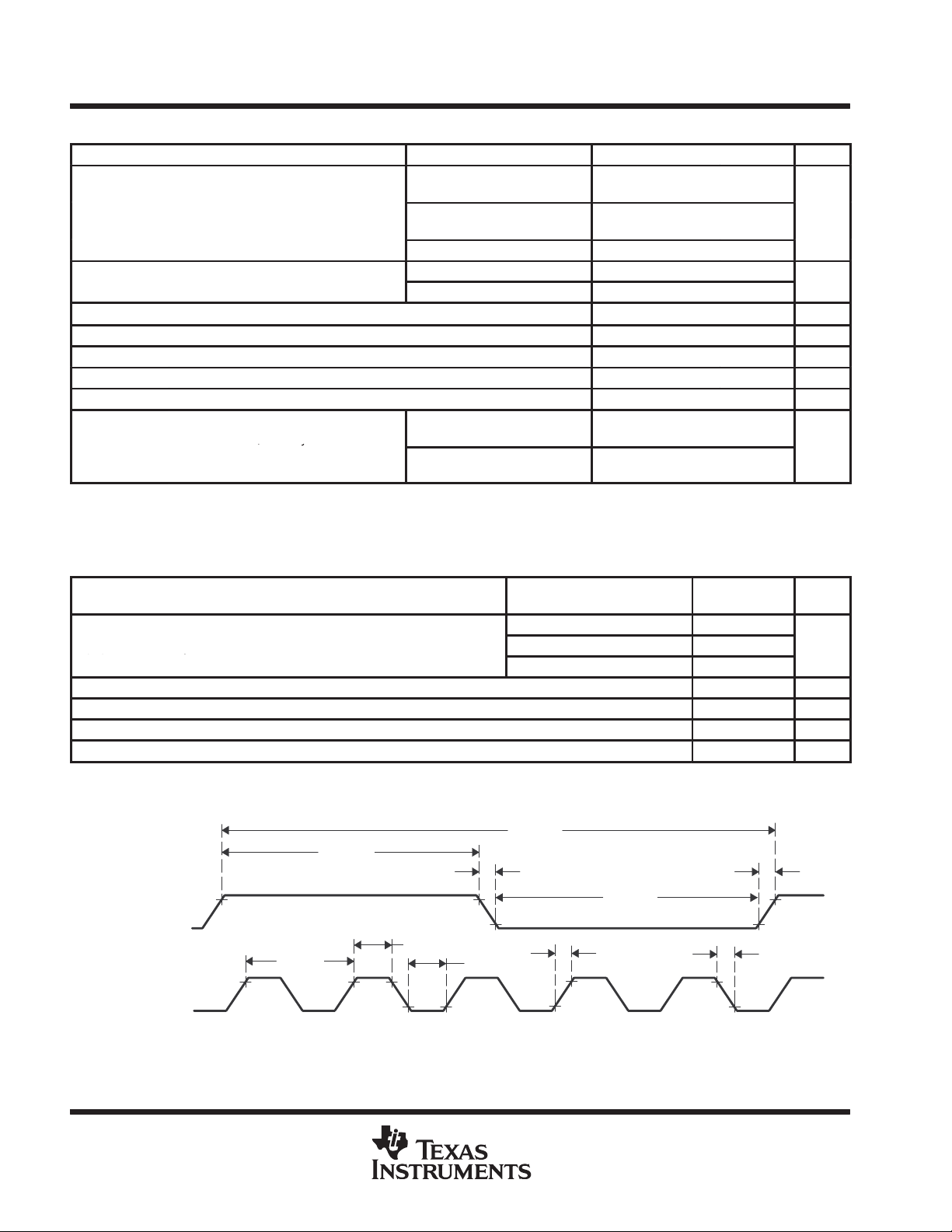
TMS320C240, TMS320F240
t
Cycle ti
SYSCLK
ns
t
,y
ns
()
y
DSP CONTROLLERS
SPRS042D – OCTOBER 1996 – REVISED NOVEMBER 1998
switching characteristics over recommended operating conditions [H = 0.5 t
PARAMETER CLOCK MODE MIN TYP MAX UNIT
before PLL lock,
CLKIN divide by 2
t
c(CPU)
c(SYS)
t
c(CO)
t
f(CO)
t
r(CO)
t
w(COL)
t
w(COH)
p
†
This device utilizes a fully static design and, therefore, can operate with input clock cycle time [t
characterized at frequencies approaching 0 Hz.
‡
SYSCLK is initialized to divide-by-4 mode by any device reset.
Cycle time, CPUCLK
me,
Cycle time, CLKOUT
Fall time, CLKOUT 5 ns
Rise time, CLKOUT 5 ns
Pulse duration, CLKOUT low H–10 H–6 H–1 ns
Pulse duration, CLKOUT high H+0 H+4 H+8 ns
Transition time, PLL synchronized after
PLL enabled
before PLL lock,
CLKIN divide by 1
after PLL lock 50
CPUCLK divide by 2 2t
CPUCLK divide by 4
before PLL lock,
CLKIN divide by 2
before PLL lock,
CLKIN divide by 1
‡
c(CPU)
4t
c(CPU)
50 † ns
] approaching infinity. The device is
c(CI)
2t
t
] (see Figure 22)
c(CO)
c(Cl)
c(Cl)
2000t
1000t
c(Cl)
c(Cl)
timing requirements over recommended operating conditions (see Note 1 and Figure 22)
EXTERNAL REFERENCE
CRYSTAL
4 MHz 250 †
t
c(Cl)
t
f(Cl)
t
r(Cl)
t
w(CIL)
t
w(CIH)
†
This device utilizes a fully static design and, therefore, can operate with input clock cycle time [t
characterized at frequencies approaching 0 Hz.
NOTE 1: Timings assume CLKOUT is set to output CPUCLK. CLKOUT is initialized to CPUCLK by power-on reset.
XTAL1/CLKIN
Cycle time, XTAL1/CLKIN
Fall time, XTAL1/CLKIN 5 ns
Rise time, XTAL1/CLKIN 5 ns
Pulse duration, XT AL1/CLKIN low as a percentage of t
Pulse duration, XTAL1/CLKIN high as a percentage of t
t
w(CIH)
c(CI)
c(CI)
t
c(CI)
t
6 MHz
8 MHz 125
c(CI)
f(Cl)
t
w(CIL)
] approaching infinity. The device is
MIN MAX UNIT
167
40 60 %
40 60 %
t
r(Cl)
†
ns
†
ns
t
CLKOUT
t
c(CO)
w(COH)
t
w(COL)
t
r(CO)
t
f(CO)
Figure 22. CLKIN-to-CLKOUT Timings for PLL Oscillator Mode, Multiply-by-5 Option With 4-MHz Crystal
68
POST OFFICE BOX 1443 • HOUSTON, TEXAS 77251–1443
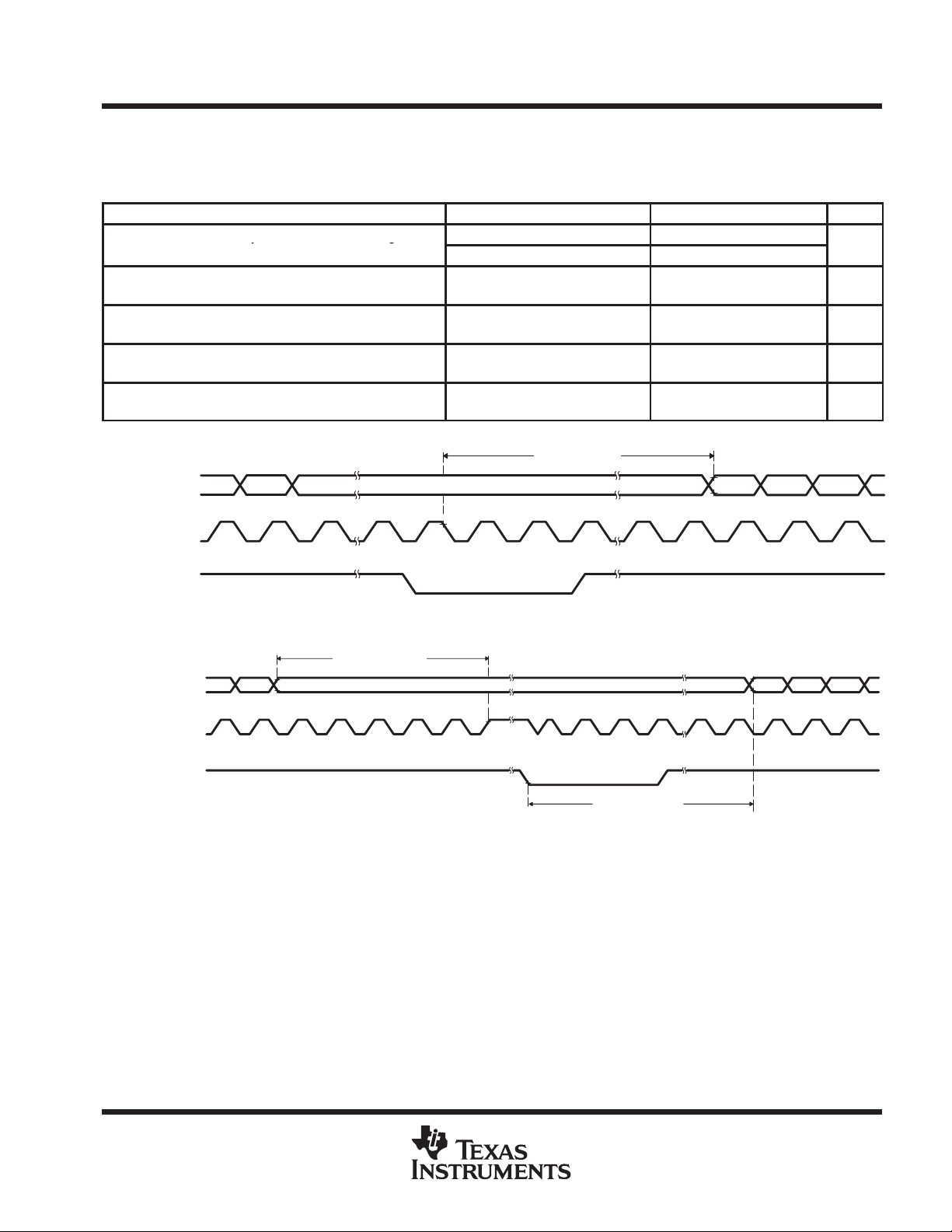
t
y, g
ns
low-power mode timings
TMS320C240, TMS320F240
DSP CONTROLLERS
SPRS042D – OCTOBER 1996 – REVISED NOVEMBER 1998
switching characteristics over recommended operating conditions [H = 0.5 t
c(CO)
(see Figure 23, Figure 24, Figure 25, and Figure 26)
PARAMETER LOW-POWER MODES MIN TYP MAX UNIT
d(WAKE-A)
t
d(IDLE-COH)
t
d(WAKE-LOCK)
t
d(WAKE-OSC)
t
d(IDLE-OSC)
NOTE 1: Timings assume CLKOUT is set to output CPUCLK. CLKOUT is initialized to CPUCLK by power-on reset.
A0–A15
CLKOUT/IOPC1
WAKE INT
Delay time, CLKOUT switching to
program execution resume (see Note 1)
Delay time, Idle instruction executed to
CLKOUT high (see Note 1)
Delay time, CLKOUT switching to PLL
synchronized (see Note 1)
Delay time, wakeup interrupt asserted
to oscillator running
Delay time, Idle instruction executed to
oscillator power off
Figure 23. IDLE1 Entry and Exit Timings
Idle 1 and Idle 2 15 X t
PLL or OSC power down
Idle 2, PLL power down, OSC
power down
PLL or OSC power down 100 µs
OSC power down 10 ms
OSC power down 60 µs
t
d(WAKE–A)
15 X t
]
c(CO)
c(CI)
500 ns
A0–A15
CLKOUT/IOPC1
WAKE INT
t
d(IDLE–COH)
t
d(WAKE–A)
Figure 24. IDLE2 Entry and Exit Timings
POST OFFICE BOX 1443 • HOUSTON, TEXAS 77251–1443
69
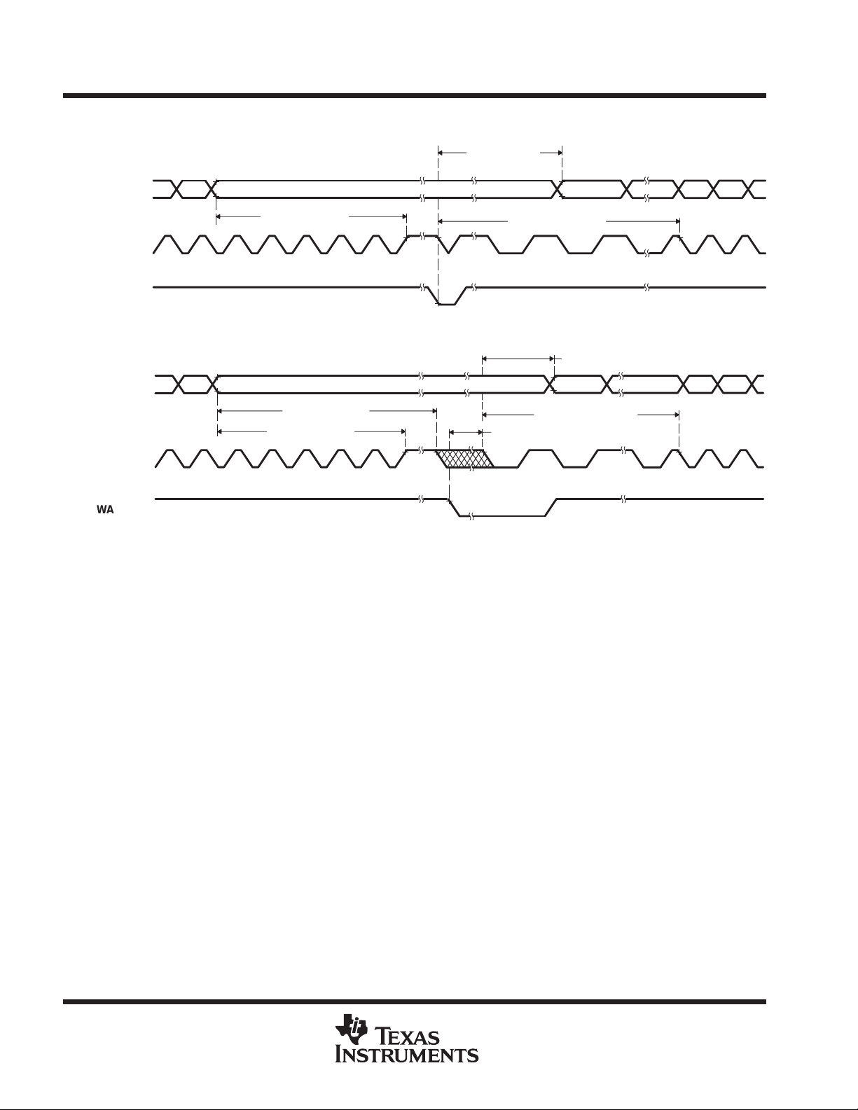
TMS320C240, TMS320F240
DSP CONTROLLERS
SPRS042D – OCTOBER 1996 – REVISED NOVEMBER 1998
low-power mode timings (continued)
A0–A15
t
d(WAKE–A)
CLKOUT/IOPC1
WAKE INT
A0–A15
CLKOUT/IOPC1
WAKE INT
t
d(IDLE–COH)
t
d(WAKE–LOCK)
Figure 25. PLL Power-Down Entry and Exit Timings
t
d(WAKE–A)
t
d(IDLE–OSC)
t
d(IDLE–COH)
t
t
d(WAKE–LOCK)
d(WAKE–OSC)
Figure 26. OSC Power-Down Entry and Exit Timings
70
POST OFFICE BOX 1443 • HOUSTON, TEXAS 77251–1443
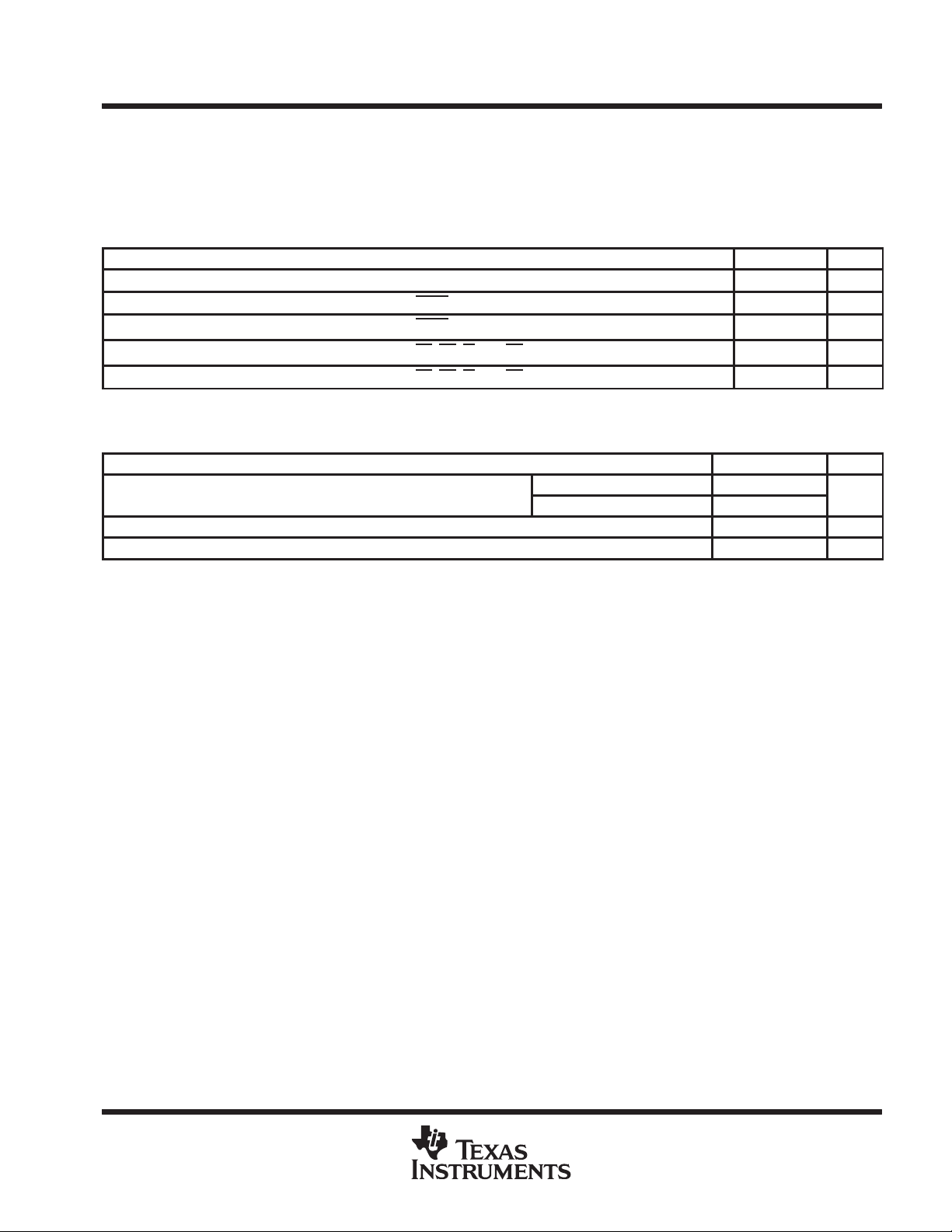
t
A
lid t
ns
TMS320C240, TMS320F240
DSP CONTROLLERS
SPRS042D – OCTOBER 1996 – REVISED NOVEMBER 1998
MEMORY AND PERIPHERAL INTERFACE TIMINGS
read
memory and parallel I/O interface
switching characteristics over recommended operating conditions for a memory read
@ 5 V [H = 0.5t
t
d(CO-A)RD
t
d(CO-SL)RD
t
d(CO-SH)RD
t
d(CO-ACTL)RD
t
d(CO-ACTH)RD
] (see Figure 27)
c(CO)
Delay time, CLKOUT/IOPC1 low to address valid
Delay time, CLKOUT/IOPC1 low to STRB low
Delay time, CLKOUT/IOPC1 low to STRB high
Delay time, CLKOUT/IOPC1 low to PS, DS, IS, and BR low
Delay time, CLKOUT/IOPC1 low to PS, DS, IS, and BR high
timing requirements over recommended operating conditions for a memory read
@ 5 V [H = 0.5t
a(A)
t
su(D-COL)RD
t
h(COL-D)RD
†
All timings with respect to CLKOUT/IOPC1 assume CLKSRC[1:0] bits are set to select CPUCLK for output.
ccess time, from address va
Setup time, data read before CLKOUT/IOPC1 low 15 ns
Hold time, data read after CLKOUT/IOPC1 low 2 ns
]† (see Figure 27)
c(CO)
timings
PARAMETER MIN MAX UNIT
MIN MAX UNIT
o read data
0 wait state 2H – 32
1 wait state
4H – 32
17 ns
10 ns
6 ns
10 ns
10 ns
POST OFFICE BOX 1443 • HOUSTON, TEXAS 77251–1443
71
TMS320C240, TMS320F240
DSP CONTROLLERS
SPRS042D – OCTOBER 1996 – REVISED NOVEMBER 1998
MEMORY AND PERIPHERAL INTERFACE TIMINGS (CONTINUED)
memory and parallel I/O interface
CLKOUT/IOPC1
PS, DS, IS,
or BR
A0–A15
W/R
read
t
d(CO–ACTL)RD
t
d(CO–A)RD
timings (continued)
t
d(CO–A)RD
t
d(CO–ACTH)RD
WE
D0–D15
STRB
READY
t
su(D-COL)RD
t
a(A)
t
d(CO–SL)RD
Figure 27. Memory Interface
t
h(COL-D)RD
Read
Timings
t
d(CO–SH)RD
72
POST OFFICE BOX 1443 • HOUSTON, TEXAS 77251–1443

MEMORY AND PERIPHERAL INTERFACE TIMINGS (CONTINUED)
memory and parallel I/O interface
write
TMS320C240, TMS320F240
DSP CONTROLLERS
SPRS042D – OCTOBER 1996 – REVISED NOVEMBER 1998
timings
switching characteristics over recommended operating conditions for a memory write
†
]
@ 5 V [H = 0.5t
t
d(CO-A)W
t
d(CO-D)
t
h(WH-A)
t
w(WH)
t
w(WL)
t
d(CO-WL)
t
d(CO-WH)
t
su(D-WH)
t
hz(WH-D)
t
d(CO-SL)W
t
d(CO-SH)W
t
d(CO-ACTL)W
t
d(CO-ACTH)W
t
d(CO-RWL)
t
d(CO-RWH)
†
All timings with respect to CLKOUT/IOPC1 assume CLKSRC[1:0] bits are set to select CPUCLK for output.
‡
MIN value for ’C240 only
c(CO)
Delay time, CLKOUT/IOPC1 high to address valid
Delay time, CLKOUT/IOPC1 low to data bus driven
Hold time, address valid after WE high
Pulse duration, WE high
Pulse duration, WE low 2H – 11
Delay time, CLKOUT/IOPC1 low to WE low
Delay time, CLKOUT/IOPC1 low to WE high
Setup time, write data valid before WE high
High-impedance time, WE high to data bus Hi-Z
Delay time, CLKOUT/IOPC1 low to STRB low
Delay time, CLKOUT/IOPC1 low to STRB high
Delay time, CLKOUT/IOPC1 high to PS, DS, IS, and BR low
Delay time, CLKOUT/IOPC1 high to PS, DS, IS, and BR high
Delay time, CLKOUT/IOPC1 high to R/W low
Delay time, CLKOUT/IOPC1 high to R/W high
(see Figure 28)
PARAMETER MIN MAX UNIT
H – 8
‡
H – 10
2H – 11 ns
2H – 8 ns
0 5 ns
17 ns
15 ns
ns
9 ns
9 ns
10 ns
6 ns
10 ns
10 ns
10 ns
10 ns
POST OFFICE BOX 1443 • HOUSTON, TEXAS 77251–1443
73

TMS320C240, TMS320F240
DSP CONTROLLERS
SPRS042D – OCTOBER 1996 – REVISED NOVEMBER 1998
MEMORY AND PERIPHERAL INTERFACE TIMINGS (CONTINUED)
memory and parallel I/O interface
CLKOUT/IOPC1
PS, DS, IS,
or BR
A0–A15
write
t
d(CO–ACTL)W
timings (continued)
t
d(CO–A)W
t
h(WH-A)
t
d(CO–ACTH)W
R/W
W/R
WE
D0–D15
STRB
READY
t
d(CO–RWL)
t
t
d(CO–SL)W
t
d(CO–WL)
d(CO–D)
Figure 28. Memory Interface
t
w(WH)
t
su(D-WH)
t
d(CO–WH)
Write
Timings
t
d(CO–RWH)
t
hz(WH-D)
t
d(CO–SH)W
74
POST OFFICE BOX 1443 • HOUSTON, TEXAS 77251–1443
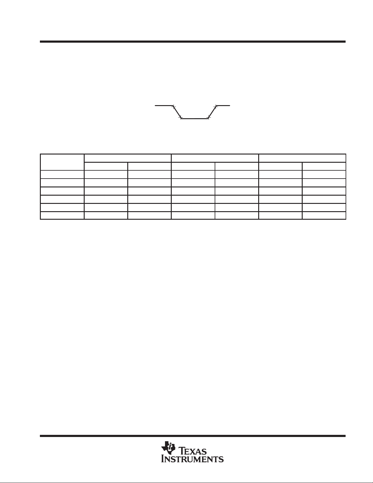
SPRS042D – OCTOBER 1996 – REVISED NOVEMBER 1998
I/O timing variation with load capacitance: SPICE simulation results
TMS320C240, TMS320F240
DSP CONTROLLERS
Condition: Temperature
Capacitance
Voltage
: – 40 to 150° C
: 5–125pF
: 5.0 V
2.2 V
0.8 V
Figure 29. Rise and Fall Time Diagram
Table 19. Timing Variation With Load Capacitance: [VCC = 5 V, VOH = 2.2 V, VOL = 0.8 V]
– 40°C 27°C 150°C
RISE FALL RISE FALL RISE FALL
5 pF 2.5 ns 3.6 ns 3.1 ns 4.5 ns 4.3 ns 6.2 ns
25 pF 3.1 ns 4.6 ns 4.0 ns 5.7 ns 5.6 ns 7.8 ns
50 pF 3.9 ns 5.9 ns 5.0 ns 7.3 ns 7.2 ns 9.9 ns
75 pF 4.7 ns 7.3 ns 6.1 ns 8.9 ns 8.8 ns 11.7 ns
100 pF 5.4 ns 8.9 ns 7.2 ns 10.6 ns 10.5 ns 13.8 ns
125 pF 6.2 ns 10.4 ns 8.3 ns 12.2 ns 12.1 ns 15.8 ns
POST OFFICE BOX 1443 • HOUSTON, TEXAS 77251–1443
75

TMS320C240, TMS320F240
DSP CONTROLLERS
SPRS042D – OCTOBER 1996 – REVISED NOVEMBER 1998
READY timings
timing requirements over recommended operating conditions [H = 0.5t
t
su(R-CO)
t
h(CO-R)
t
v(R)ARD
t
v(R)AW
†
The READY timings are based on one software wait state. At full speed operation, the ’x240 does not allow for single READY -based wait states.
‡
MIN value for ’C240 only
§
MAX values for ’C240 only
CLKOUT/IOPC1
PS, DS, or IS
Setup time, READY low before CLKOUT/IOPC1 high
Hold time, READY low after CLKOUT/IOPC1 high
Valid time, READY after address valid on read
Valid time, READY after address valid on write
A0–A15
]† (see Figure 30)
c(CO)
MIN MAX UNIT
14
‡
16
0 ns
3H – 31
3H – 33
4H – 31
4H – 33
ns
ns
§
ns
§
W/R
WE
D0–D15
STRB
READY
t
v(R)ARD
t
su(R–CO)
t
h(CO–R)
Figure 30. READY Timings
t
v(R)AW
76
POST OFFICE BOX 1443 • HOUSTON, TEXAS 77251–1443

RS and PORESET timings
TMS320C240, TMS320F240
DSP CONTROLLERS
SPRS042D – OCTOBER 1996 – REVISED NOVEMBER 1998
switching characteristics over recommended operating conditions for a reset [H = 0.5t
(see Figure 31 and Figure 32)
PARAMETER MIN MAX UNIT
t
w(RSL1)
t
d(RS)
t
d(EX)
†
The parameter t
Pulse duration, RS low
Delay time, RS low to program address at reset vector
Delay time, RS high to reset vector executed
w(RSL1)
refers to the time RS is an output.
timing requirements over recommended operating conditions for a reset [H = 0.5t
†
8t
c(SYS)
4H ns
32H ns
c(CO)
(see Figure 31 and Figure 32)
MIN MAX UNIT
t
w(RSL)
‡
The parameter t
V
XTAL1/CLKIN
Pulse duration, RS or PORESET low
refers to the time RS is an input.
w(RSL)
CC
‡
5 ns
c(CO)
]
]
ns
PORESET
†
PORESET
‡
RS
a 2.7-kΩ resistor in series with a totem pole drive circuit. If RS
†
‡
RS
is required to be driven low during power up to ensure all clock/PLL registers are reset to a known state.
is a bidirectional (open-drain output) pin and can be optionally pulled low through an open-drain or open-collector drive circuit, or through
is left undriven, then a 20-kΩ pullup resistor should be used.
Figure 31. Reset Timings
POST OFFICE BOX 1443 • HOUSTON, TEXAS 77251–1443
77

TMS320C240, TMS320F240
DSP CONTROLLERS
SPRS042D – OCTOBER 1996 – REVISED NOVEMBER 1998
RS and PORESET timings (continued)
t
w(RSL)
PORESET
†
RS
t
w(RSL1)
t
d(RS)
A0–A15
†
RS is driven low by any device reset, which includes asserting PORESET , RS, access to an illegal address, execution of a software
reset, or a watchdog timer reset.
0000h 0001h
t
d(EX)
Figure 32. Power-On Reset Timings
78
POST OFFICE BOX 1443 • HOUSTON, TEXAS 77251–1443

XF, BIO, and MP/MC timings
TMS320C240, TMS320F240
DSP CONTROLLERS
SPRS042D – OCTOBER 1996 – REVISED NOVEMBER 1998
switching characteristics over recommended operating conditions [H = 0.5t
PARAMETER MIN MAX UNIT
t
d(XF)
timing requirements over recommended operating conditions [H = 0.5t
t
w(BIOL)
t
w(MPMCV)
†
This is the minimum time the MP/MC
must maintain a valid level for the duration of the entire memory access (or accesses) on- or off-chip.
CLKOUT/IOPC1
Delay time, CLKOUT high to XF high/low
Pulse duration, BIO low
Pulse duration, MP/MC valid
pin needs to be stable in order to be recognized by internal logic; however, for proper operation, the user
t
d(XF)
XF
MP/MC
†
t
w(MPMCV)
c(CO)
†
Valid
] (see Figure 33)
c(CO)
11 ns
] (see Figure 33)
MIN MAX UNIT
2H + 16 ns
2H + 24 ns
t
w(BIOL)
BIO
†
This is the minimum time the MP/MC
operation, the user must maintain a valid level for the duration of the entire memory access (or accesses) on- or off-chip.
pin needs to be stable in order to be recognized by internal logic; however, for proper
Figure 33. XF, BIO, and MP/MC Timings
POST OFFICE BOX 1443 • HOUSTON, TEXAS 77251–1443
79
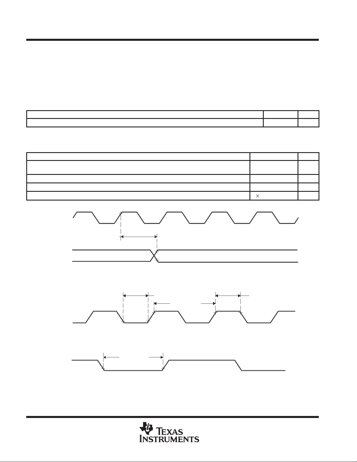
TMS320C240, TMS320F240
DSP CONTROLLERS
SPRS042D – OCTOBER 1996 – REVISED NOVEMBER 1998
TIMING EVENT MANAGER INTERFACE
PWM/CMP timings
PWM refers to PWM1/CMP1, PWM2/CMP2, PWM3/CMP3, PWM4/CMP4, PWM5/CMP5, PWM6/CMP6,
T1PWM/T1CMP, T2PWM/T2CMP, T3PWM/T3CMP, PWM7/CMP7, PWM8/CMP8, and PWM9/CMP9.
switching characteristics over recommended operating conditions for PWM timing
[H = 0.5t
t
d(PWM)CO
] (see Figure 34)
c(CO)
PARAMETER MIN MAX UNIT
Delay time, CLKOUT high to PWM output switching
12 ns
timing requirements over recommended operating conditions for PWM timing [H = 0.5t
(see Figure 35 and Figure 36)
MIN MAX UNIT
t
w(TMRDIR)
t
w(TMRCLKL)
t
w(TMRCLKH)
t
c(TMRCLK)
†
MIN value for ’C240 only
CLKOUT/IOPC1
PWM
Pulse duration, TMRDIR low/high
Pulse duration, TMRCLK low as a percentage of TMRCLK cycle time
Pulse duration, TMRCLK high as a percentage of TMRCLK cycle time
Cycle time, TMRCLK
t
d(PWM)CO
Figure 34. PWM and Compare Output Timings
t
w(TMRCLKL)
t
c(TMRCLK)
4H + 12
†
4H + 14
40 60 %
40 60 %
4 t
c(CPU)
t
w(TMRCLKH)
c(CO)
]
ns
ns
80
TMRCLK
TMRDIR
Figure 35. External Timer Clock Input Timings
t
w(TMRDIR)
Figure 36. External Timer Direction Input Timings
POST OFFICE BOX 1443 • HOUSTON, TEXAS 77251–1443
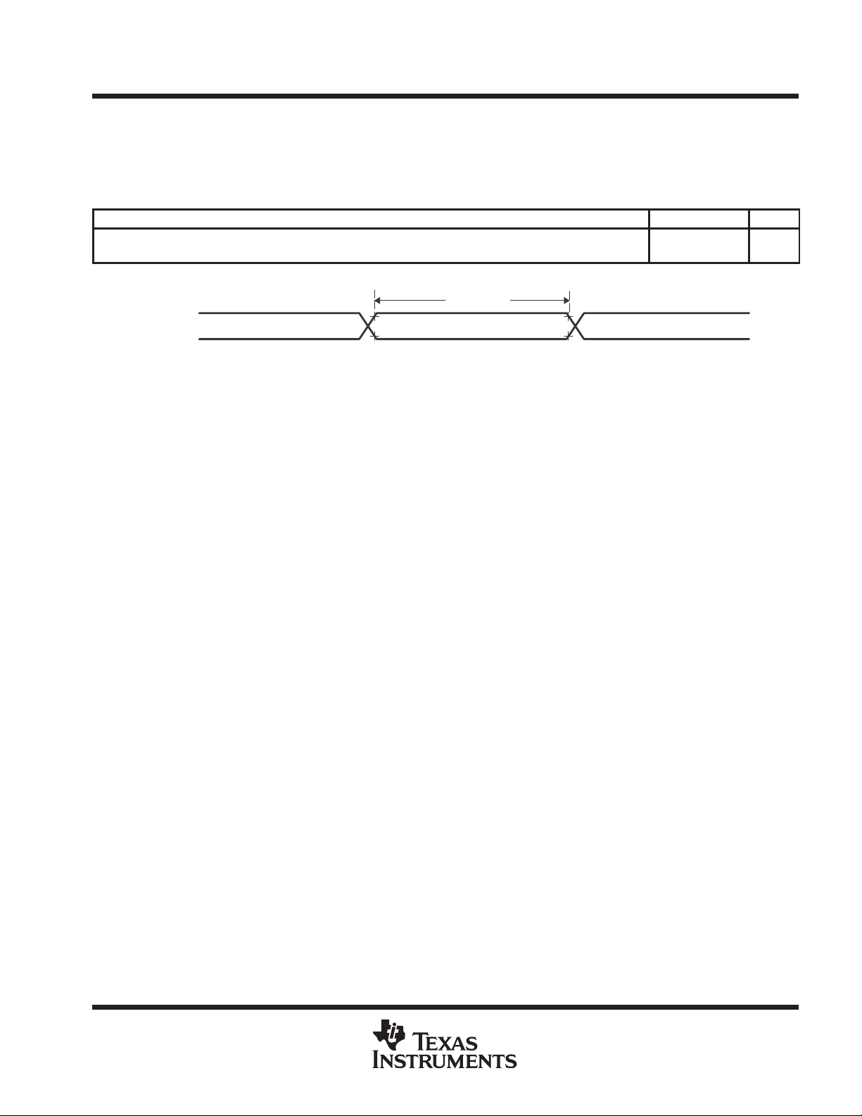
SPRS042D – OCTOBER 1996 – REVISED NOVEMBER 1998
TMS320C240, TMS320F240
capture and QEP timings
CAP refers to CAP1/QEP1/IOPC4, CAP2/QEP2/IOPC5, CAP3/IOPC6, and CAP4/IOPC7.
DSP CONTROLLERS
timing requirements over recommended operating conditions for CAP [H = 0.5t
(see Figure 37)
t
w(CAP)
†
MIN value for ’C240 only
Pulse duration, CAP input low/high
CAP
t
w(CAP)
Figure 37. Capture and QEP Input Timings
4H + 12
4H + 15
]
c(CO)
MIN MAX UNIT
†
ns
POST OFFICE BOX 1443 • HOUSTON, TEXAS 77251–1443
81

TMS320C240, TMS320F240
DSP CONTROLLERS
SPRS042D – OCTOBER 1996 – REVISED NOVEMBER 1998
interrupt timings
PWM refers to PWM1/CMP1, PWM2/CMP2, PWM3/CMP3, PWM4/CMP4, PWM5/CMP5, PWM6/CMP6,
T1PWM/T1CMP, T2PWM/T2CMP, T3PWM/T3CMP, PWM7/CMP7, PWM8/CMP8, and PWM9/CMP9.
INT refers to NMI, XINT1, XINT2/IO, and XINT3/IO. PDP refers to PDPINT.
switching characteristics over recommended operating conditions for interrupts [H = 0.5t
(see Figure 39)
PARAMETER MIN MAX UNIT
t
d(PWM)PDP
Delay time, PDPINT low to PWM to high-impedance state
0 15 ns
timing requirements over recommended operating conditions for interrupts [H = 0.5t
(see Figure 38 and Figure 39)
MIN MAX UNIT
t
w(INT)
t
w(PDP)
t
d(INT)
Pulse duration, INT input low/high
Pulse duration, PDPINT input low
Delay time, INT low/high to interrupt-vector fetch
INT
Figure 38. External Interrupt Timings
PDPINT
t
w(INT)
2t
c(SYS)
t
w(PDP)
t
+ 12 ns
c(SYS)
2H + 18 ns
+ 4t
c(CPU)
c(CO)
c(CO)
ns
]
]
PWM
t
d(PWM)PDP
Figure 39. Power-Drive Protection Interrupt Timings
82
POST OFFICE BOX 1443 • HOUSTON, TEXAS 77251–1443
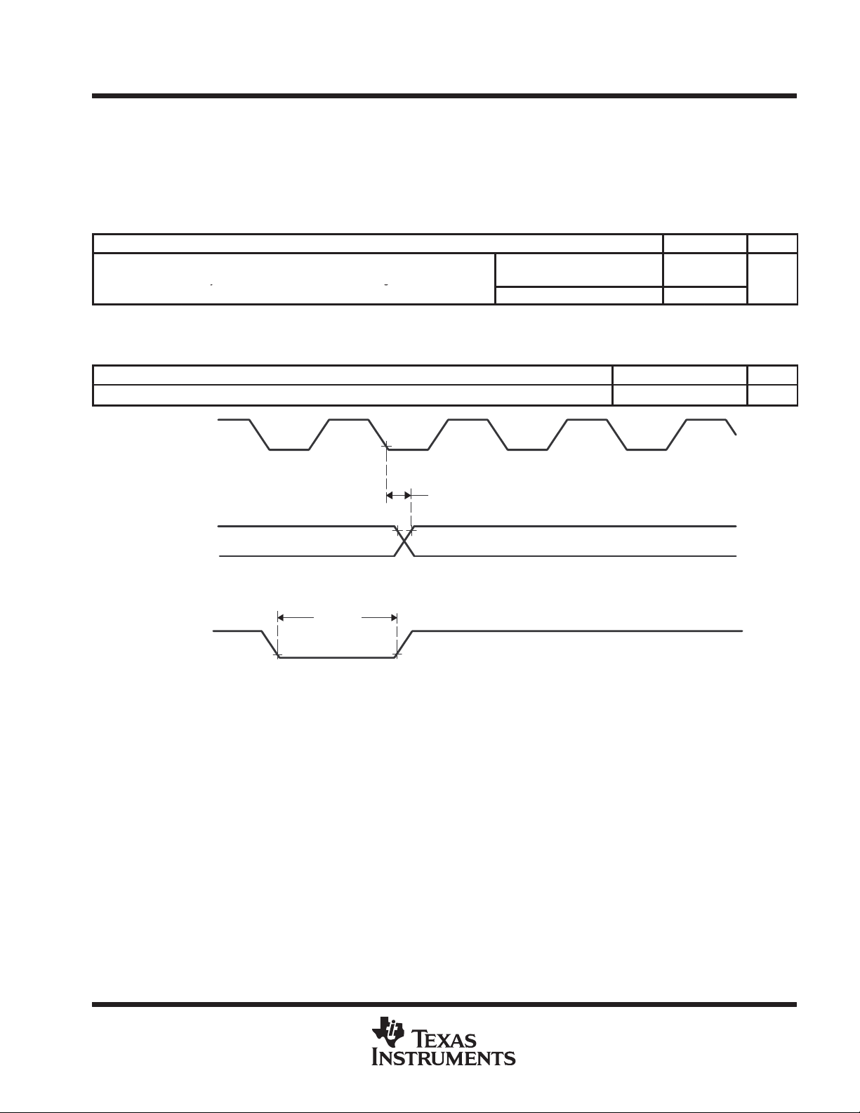
d(GPO)CO
y, g
TMS320C240, TMS320F240
DSP CONTROLLERS
SPRS042D – OCTOBER 1996 – REVISED NOVEMBER 1998
general-purpose input/output timings
GPO refers to the digital output function of shared pins IOPA0–3, IOPB0–7, IOPC0–7, XINT2/IO, XINT3/IO.
GPI refers to the digital input function of shared pins IOPA0–3, IOPB0–7, IOPC0–7, XINT2/IO, XINT3/IO.
switching characteristics over recommended operating conditions for a GPI/O [H = 0.5t
(see Figure 40)
PARAMETER MIN MAX UNIT
XINT2/IO, XINT3/IO, IOPB6,
t
Delay time, CLKOUT low to GPO low/high
timing requirements over recommended operating conditions for a GPI/O [H = 0.5t
IOPB7, and IOPC0
All other GPOs 25
c(CO)
(see Figure 41)
MIN MAX UNIT
t
w(GPI)
CLKOUT/IOPC1
Pulse duration, GPI high/low
GPO
t
d(GPO)CO
Figure 40. General-Purpose Output Timings
t
+ 12 ns
c(SYS)
c(CO)
33
]
]
ns
GPI
t
w(GPI)
Figure 41. General-Purpose Input Timings
POST OFFICE BOX 1443 • HOUSTON, TEXAS 77251–1443
83
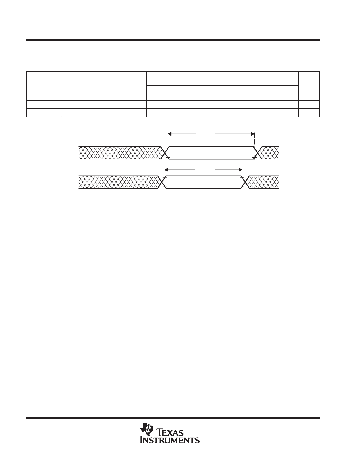
TMS320C240, TMS320F240
DSP CONTROLLERS
SPRS042D – OCTOBER 1996 – REVISED NOVEMBER 1998
SERIAL COMMUNICATIONS INTERFACE (SCI) I/O TIMINGS
timing characteristics for SCI (see Note 2 and Figure 42)
(BRR + 1)
PARAMETER
t
c(SCC)
t
v(TXD)
t
v(RXD)
NOTE 2: tc = system clock cycle time = 1/SYSCLK = t
Cycle time, SCICLK 16t
Valid time, SCITXD data t
Valid time, SCIRXD data 16t
c(SYS)
IS EVEN AND BRR = 0
MIN MAX MIN MAX
c
–70 t
c(SCC)
c
65536t
c(SCC)
t
v(TXD)
c
+70 t
(BRR + 1)
IS ODD AND BRR ≠ 0
24t
c
–70 t
c(SCC)
24t
c
c(SCC)
65535t
+70 ns
UNIT
ns
c
ns
SCITXD
SCIRXD
Data Valid
t
v(RXD)
Data Valid
Figure 42. SCI Timings
84
POST OFFICE BOX 1443 • HOUSTON, TEXAS 77251–1443

POST OFFICE BOX 1443 HOUSTON, TEXAS 77251–1443
ns
ns
ns
ns
ns
ns
• 85
SPI MASTER MODE TIMING PARAMETERS
SPI master mode timing information is listed in the following tables.
SPI master mode external timing parameters (clock phase = 0)† (see Figure 43)
WHEN (SPIBRR + 1) IS EVEN OR
SPIBRR = 0 OR 2
MIN MAX MIN MAX
t
c(SPC)M
t
w(SPCH)M
t
w(SPCL)M
t
w(SPCL)M
t
w(SPCH)M
t
d(SPCH-SIMO)M
t
d(SPCL-SIMO)M
t
v(SPCL-SIMO)M
t
v(SPCH-SIMO)M
t
su(SOMI-SPCL)M
t
su(SOMI-SPCH)M
t
v(SPCL-SOMI)M
t
v(SPCH-SOMI)M
†
The MASTER/SLA VE bit (SPICTL.2) is set and the CLOCK PHASE bit (SPICTL.3) is cleared.
‡
tc = system clock cycle time = 1/SYSCLK = t
§
The active edge of the SPICLK signal referenced is controlled by the CLOCK POLARITY bit (SPICCR.6).
§
§
§
§
Cycle time, SPICLK 4t
Pulse duration, SPICLK high (clock polarity = 0) 0.5t
Pulse duration, SPICLK low (clock polarity = 1) 0.5t
Pulse duration, SPICLK low (clock polarity = 0) 0.5t
Pulse duration, SPICLK high (clock polarity = 1) 0.5t
Delay time, SPICLK high (clock polarity = 0) to
§
SPISIMO valid
Delay time, SPICLK low (clock polarity = 1) to
§
SPISIMO valid
Valid time, SPISIMO data valid after SPICLK low
§
(clock polarity =0)
Valid time, SPISIMO data valid after SPICLK high
§
(clock polarity =1)
Setup time, SPISOMI before SPICLK low
§
(clock polarity = 0)
Setup time, SPISOMI before SPICLK high
§
(clock polarity = 1)
Valid time, SPISOMI data valid after SPICLK low
§
(clock polarity = 0)
Valid time, SPISOMI data valid after SPICLK high
§
(clock polarity = 1)
c(SYS)
0.5t
0.5t
0.25t
0.25t
‡
c
c(SPC)M
c(SPC)M
c(SPC)M
c(SPC)M
c(SPC)M
c(SPC)M
c(SPC)M
c(SPC)M
–70 0.5t
–70 0.5t
–70 0.5t
–70 0.5t
– 10 10 – 10 10
– 10 10 – 10 10
–70 0.5t
–70 0.5t
0 0
0 0
–70 0.5t
–70 0.5t
128t
c
c(SPC)M
c(SPC)M
c(SPC)M
c(SPC)M
‡
0.5t
0.5t
0.5t
0.5t
WHEN (SPIBRR + 1)
IS ODD AND SPIBRR > 3
‡
5t
c
c(SPC)M
c(SPC)M
c(SPC)M
c(SPC)M
c(SPC)M
c(SPC)M
c(SPC)M
c(SPC)M
–0.5tc–70 0.5t
–0.5tc–70 0.5t
+0.5tc–70 0.5t
+0.5tc–70 0.5t
+0.5tc–70
+0.5tc–70
–0.5tc–70
–0.5tc–70
‡
127t
c
c(SPC)M
c(SPC)M
c(SPC)M
c(SPC)M
– 0.5t
–0.5t
+ 0.5t
+ 0.5t
UNIT
ns
c
c
c
c
SPRS042D – OCTOBER 1996 – REVISED NOVEMBER 1998
TMS320C240, TMS320F240
DSP CONTROLLERS
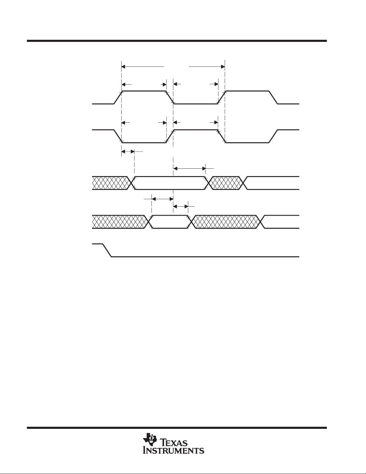
TMS320C240, TMS320F240
DSP CONTROLLERS
SPRS042D – OCTOBER 1996 – REVISED NOVEMBER 1998
PARAMETER MEASUREMENT INFORMATION
t
c(SPC)M
(clock polarity = 0)
SPICLK
SPICLK
(clock polarity = 1)
SPISIMO
SPISOMI
SPISTE
t
su(SOMI-SPCL)M
t
su(SOMI-SPCH)M
†
t
w(SPCH)M
t
w(SPCL)M
t
d(SPCH-SIMO)M
t
d(SPCL-SIMO)M
Master Out Data Is Valid
Master In Data
Must Be Valid
t
w(SPCL)M
t
w(SPCH)M
t
v(SPCL-SOMI)M
t
v(SPCH-SOMI)M
t
v(SPCH-SIMO)M
t
v(SPCL-SIMO)M
†
The SPISTE signal must be active before the SPI communication stream starts; the SPISTE signal must remain active
until the SPI communication stream is complete.
Figure 43. SPI Master Mode External Timings (Clock Phase = 0)
86
POST OFFICE BOX 1443 • HOUSTON, TEXAS 77251–1443

POST OFFICE BOX 1443 HOUSTON, TEXAS 77251–1443
ns
ns
ns
ns
• 87
SPI master mode external timing parameters (clock phase = 1)† (see Figure 44)
WHEN (SPIBRR + 1) IS EVEN OR
SPIBRR = 0 OR 2
MIN MAX MIN MAX
0.5t
0.5t
0.5t
0.5t
0.5t
0.5t
0.25t
0.25t
‡
c
c(SPC)M
c(SPC)M
c(SPC)M
c(SPC)M
c(SPC)M
c(SPC)M
c(SPC)M
c(SPC)M
c(SPC)M
c(SPC)M
–70 0.5t
–70 0.5t
–70 0.5t
–70 0.5t
–70 0.5t
–70 0.5t
–70 0.5t
–70 0.5t
0 0
0 0
–70 0.5t
–70 0.5t
t
c(SPC)M
t
w(SPCH)M
t
w(SPCL)M
t
w(SPCL)M
t
w(SPCH)M
t
su(SIMO-SPCH)M
t
su(SIMO-SPCL)M
t
v(SPCH-SIMO)M
t
v(SPCL-SIMO)M
t
su(SOMI-SPCH)M
t
su(SOMI-SPCL)M
t
v(SPCH-SOMI)M
t
v(SPCL-SOMI)M
†
The MASTER/SLA VE bit (SPICTL.2) is set and the CLOCK PHASE bit (SPICTL.3) is set.
‡
tc = system clock cycle time = 1/SYSCLK = t
§
The active edge of the SPICLK signal referenced is controlled by the CLOCK POLARITY bit (SPICCR.6).
§
§
§
§
Cycle time, SPICLK 4t
Pulse duration, SPICLK high
(clock polarity = 0)
Pulse duration, SPICLK low (clock polarity = 1) 0.5t
Pulse duration, SPICLK low (clock polarity = 0) 0.5t
Pulse duration, SPICLK high
(clock polarity = 1)
Setup time, SPISIMO data valid before SPICLK high
§
(clock polarity = 0)
Setup time, SPISIMO data valid before SPICLK low
§
(clock polarity = 1)
Valid time, SPISIMO data valid after SPICLK high
§
(clock polarity =0)
Valid time, SPISIMO data valid after SPICLK low
§
(clock polarity =1)
Setup time, SPISOMI before SPICLK high
§
(clock polarity = 0)
Setup time, SPISOMI before SPICLK low
§
(clock polarity = 1)
Valid time, SPISOMI data valid after SPICLK high
§
(clock polarity = 0)
Valid time, SPISOMI data valid after SPICLK low
§
(clock polarity = 1)
c(SYS)
128t
c(SPC)M
c(SPC)M
c(SPC)M
c(SPC)M
‡
c
0.5t
0.5t
0.5t
0.5t
WHEN (SPIBRR + 1)
IS ODD AND SPIBRR > 3
‡
5t
c
c(SPC)M
c(SPC)M
c(SPC)M
c(SPC)M
–0.5tc–70 0.5t
–0.5tc–70 0.5t
+0.5tc–70 0.5t
+0.5tc–70 0.5t
c(SPC)M
c(SPC)M
c(SPC)M
c(SPC)M
c(SPC)M
c(SPC)M
–70
–70
–70
–70
–70
–70
127t
c
c(SPC)M
c(SPC)M
c(SPC)M
c(SPC)M
UNIT
‡
–0.5t
–0.5t
+ 0.5t
+ 0.5t
ns
c
ns
c
c
ns
c
SPRS042D – OCTOBER 1996 – REVISED NOVEMBER 1998
TMS320C240, TMS320F240
DSP CONTROLLERS

TMS320C240, TMS320F240
DSP CONTROLLERS
SPRS042D – OCTOBER 1996 – REVISED NOVEMBER 1998
PARAMETER MEASUREMENT INFORMATION
t
c(SPC)M
(clock polarity = 0)
SPICLK
SPICLK
(clock polarity = 1)
SPISIMO
SPISOMI
SPISTE
t
su(SIMO-SPCH)M
t
su(SIMO-SPCL)M
t
su(SOMI-SPCH)M
t
su(SOMI-SPCL)M
†
t
w(SPCH)M
t
w(SPCL)M
Master Out Data Is Valid
Master In Data
Must Be Valid
t
v(SPCH-SIMO)M
t
v(SPCL-SIMO)M
t
v(SPCH-SOMI)M
t
v(SPCL-SOMI)M
t
w(SPCL)M
t
w(SPCH)M
Data Valid
†
The SPISTE signal must be active before the SPI communication stream starts; the SPISTE signal must remain active until
the SPI communication stream is complete.
Figure 44. SPI Master Mode External Timings (Clock Phase = 1)
88
POST OFFICE BOX 1443 • HOUSTON, TEXAS 77251–1443
ns
ns
ns
ns
ns
ns
TMS320C240, TMS320F240
DSP CONTROLLERS
SPRS042D – OCTOBER 1996 – REVISED NOVEMBER 1998
SPI SLAVE MODE TIMING PARAMETERS
Slave mode timing information is listed in the following tables.
SPI slave mode external timing parameters (clock phase = 0)† (see Figure 45)
MIN MAX UNIT
t
c(SPC)S
t
w(SPCH)S
t
w(SPCL)S
t
w(SPCL)S
t
w(SPCH)S
t
d(SPCH-SOMI)S
t
d(SPCL-SOMI)S
t
v(SPCL-SOMI)S
t
v(SPCH-SOMI)S
t
su(SIMO-SPCL)S
t
su(SIMO-SPCH)S
t
v(SPCL-SIMO)S
t
v(SPCH-SIMO)S
†
The MASTER/SLA VE bit (SPICTL.2) is cleared and the CLOCK PHASE bit (SPICTL.3) is cleared.
‡
tc = system clock cycle time = 1/SYSCLK = t
§
The active edge of the SPICLK signal referenced is controlled by the CLOCK POLARITY bit (SPICCR.6).
§
§
§
§
Cycle time, SPICLK 8t
Pulse duration, SPICLK high (clock polarity = 0) 0.5t
Pulse duration, SPICLK low (clock polarity = 1) 0.5t
Pulse duration, SPICLK low (clock polarity = 0) 0.5t
Pulse duration, SPICLK high (clock polarity = 1) 0.5t
§
Delay time, SPICLK high (clock polarity = 0) to SPISOMI valid 0.375t
§
Delay time, SPICLK low (clock polarity = 1) to SPISOMI valid 0.375t
§
Valid time, SPISOMI data valid after SPICLK low (clock polarity =0) 0.75t
§
Valid time, SPISOMI data valid after SPICLK high (clock polarity =1) 0.75t
§
Setup time, SPISIMO before SPICLK low (clock polarity = 0) 0
§
Setup time, SPISIMO before SPICLK high (clock polarity = 1) 0
§
Valid time, SPISIMO data valid after SPICLK low (clock polarity = 0) 0.5t
§
Valid time, SPISIMO data valid after SPICLK high (clock polarity = 1) 0.5t
c(SYS)
‡
c
c(SPC)S
c(SPC)S
c(SPC)S
c(SPC)S
c(SPC)S
c(SPC)S
c(SPC)S
c(SPC)S
c(SPC)S
c(SPC)S
–70 0.5t
–70 0.5t
–70 0.5t
–70 0.5t
–70
–70
ns
c(SPC)S
c(SPC)S
c(SPC)S
c(SPC)S
POST OFFICE BOX 1443 • HOUSTON, TEXAS 77251–1443
89
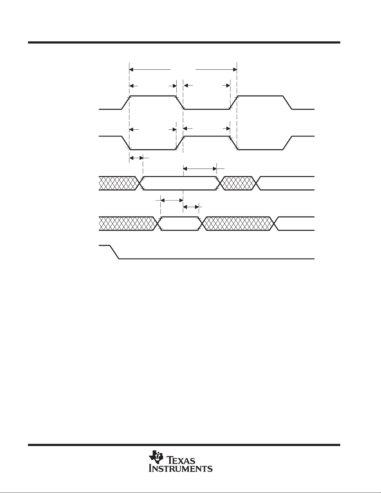
TMS320C240, TMS320F240
DSP CONTROLLERS
SPRS042D – OCTOBER 1996 – REVISED NOVEMBER 1998
PARAMETER MEASUREMENT INFORMATION
t
c(SPC)S
(clock polarity = 0)
SPICLK
SPICLK
(clock polarity = 1)
SPISOMI
SPISIMO
SPISTE
t
w(SPCH)S
t
w(SPCL)S
t
d(SPCH-SOMI)S
t
d(SPCL-SOMI)S
SPISOMI Data Is Valid
t
su(SIMO-SPCL)S
t
su(SIMO-SPCH)S
SPISIMO Data
Must Be Valid
†
t
w(SPCL)S
t
w(SPCH)S
t
v(SPCL-SIMO)S
t
v(SPCH-SIMO)S
t
v(SPCL-SOMI)S
t
v(SPCH-SOMI)S
†
The SPISTE signal must be active before the SPI communication stream starts; the SPISTE signal must remain active until
the SPI communication stream is complete.
Figure 45. SPI Slave Mode External Timing (Clock Phase = 0)
90
POST OFFICE BOX 1443 • HOUSTON, TEXAS 77251–1443
ns
ns
ns
ns
ns
ns
TMS320C240, TMS320F240
DSP CONTROLLERS
SPRS042D – OCTOBER 1996 – REVISED NOVEMBER 1998
SPI slave mode external timing parameters (clock phase = 1)† (see Figure 46)
MIN MAX UNIT
t
c(SPC)S
t
w(SPCH)S
t
w(SPCL)S
t
w(SPCL)S
t
w(SPCH)S
t
su(SOMI-SPCH)S
t
su(SOMI-SPCL)S
t
v(SPCH-SOMI)S
t
v(SPCL-SOMI)S
t
su(SIMO-SPCH)S
t
su(SIMO-SPCL)S
t
v(SPCH-SIMO)S
t
v(SPCL-SIMO)S
†
The MASTER/SLA VE bit (SPICTL.2) is cleared and the CLOCK PHASE bit (SPICTL.3) is set.
‡
tc = system clock cycle time = 1/SYSCLK = t
§
The active edge of the SPICLK signal referenced is controlled by the CLOCK POLARITY bit (SPICCR.6).
§
§
§
§
Cycle time, SPICLK 8t
Pulse duration, SPICLK high (clock polarity = 0) 0.5t
Pulse duration, SPICLK low (clock polarity = 1) 0.5t
Pulse duration, SPICLK low (clock polarity = 0) 0.5t
Pulse duration, SPICLK high (clock polarity = 1) 0.5t
§
Setup time, SPISOMI before SPICLK high (clock polarity = 0) 0.125t
§
Setup time, SPISOMI before SPICLK low (clock polarity = 1) 0.125t
§
Valid time, SPISOMI data valid after SPICLK high (clock polarity =0) 0.75t
§
Valid time, SPISOMI data valid after SPICLK low (clock polarity =1) 0.75t
§
Setup time, SPISIMO before SPICLK high (clock polarity = 0) 0
§
Setup time, SPISIMO before SPICLK low (clock polarity = 1) 0
§
Valid time, SPISIMO data valid after SPICLK high (clock polarity = 0) 0.5t
§
Valid time, SPISIMO data valid after SPICLK low (clock polarity = 1) 0.5t
c(SYS)
‡
c
c(SPC)S–70
c(SPC)S–70
c(SPC)S–70
c(SPC)S–70
c(SPC)S
c(SPC)S
c(SPC)S
c(SPC)S
c(SPC)S
c(SPC)S
0.5t
0.5t
0.5t
0.5t
ns
c(SPC)S
c(SPC)S
c(SPC)S
c(SPC)S
POST OFFICE BOX 1443 • HOUSTON, TEXAS 77251–1443
91

TMS320C240, TMS320F240
DSP CONTROLLERS
SPRS042D – OCTOBER 1996 – REVISED NOVEMBER 1998
PARAMETER MEASUREMENT INFORMATION
t
c(SPC)S
(clock polarity = 0)
SPICLK
SPICLK
(clock polarity = 1)
SPISOMI
SPISIMO
SPISTE
t
su(SOMI-SPCH)S
t
su(SOMI-SPCL)S
t
su(SIMO-SPCH)S
t
su(SIMO-SPCL)S
†
t
w(SPCH)S
t
w(SPCL)S
SPISOMI Data Is Valid
SPISIMO Data
Must Be Valid
t
v(SPCH-SOMI)S
t
v(SPCL-SOMI)S
t
v(SPCH-SIMO)S
t
v(SPCL-SIMO)S
t
w(SPCL)S
t
w(SPCH)S
Data Valid
†
The SPISTE signal must be active before the SPI communication stream starts; the SPISTE signal must remain active until
the SPI communication stream is complete.
Figure 46. SPI Slave Mode External Timing (Clock Phase = 1)
92
POST OFFICE BOX 1443 • HOUSTON, TEXAS 77251–1443

10-bit dual analog-to-digital converter (ADC)
TMS320C240, TMS320F240
DSP CONTROLLERS
SPRS042D – OCTOBER 1996 – REVISED NOVEMBER 1998
The 10-bit dual ADC has a separate power bus for its analog circuitry . These pins are referred to as V
V
. The purpose is to enhance ADC performance by preventing digital switching noise of the logic circuitry
SSA
that can be present on VSS and VCC from coupling into the ADC analog stage. All ADC specifications are given
with respect to V
unless otherwise noted.
SSA
Resolution 10-bit (1024 values). . . . . . . . . . . . . . . . . . . . . . . . . . . . . . . . . . . . . . . . . . . . . . . . . . . . . . . . . . . . . . . . . . .
Monotonic Assured. . . . . . . . . . . . . . . . . . . . . . . . . . . . . . . . . . . . . . . . . . . . . . . . . . . . . . . . . . . . . . . . . . . . . . . . . . . . . .
Output conversion mode 000h to 3FFh (000h for V
≤ V
I
; 3FFh for VI ≥ V
SSA
recommended operating conditions
MIN NOM MAX UNIT
V
CCA
V
SSA
V
REFHI
V
REFLO
V
AI
†
V
REFHI
Analog supply voltage 4.5 5 5.5 V
Analog ground 0 V
Analog supply reference source
Analog ground reference source
Analog input voltage, ADCIN0–ADCIN15 V
and V
must be stable, within ±1/2 LSB of the required resolution, during the entire conversion time.
REFLO
†
†
V
REFLO
V
SSA
SSA
V
V
CCA
REFHI
V
CCA
CCA
and
CCA
V
V
V
). . . . . . . . . . . . . . . . . . . . . . .
POST OFFICE BOX 1443 • HOUSTON, TEXAS 77251–1443
93
TMS320C240, TMS320F240
V
V
I
CCA
Analog su ly current
mA
CaiAnalog input capacitance
y
pF
DSP CONTROLLERS
SPRS042D – OCTOBER 1996 – REVISED NOVEMBER 1998
operating characteristics over recommended operating condition ranges
PARAMETER DESCRIPTION MIN MAX UNIT
= 5.5
CCA
pp
V
= V
CCA
I
ref
Z
AI
E
DNL
E
INL
t
d(PU)
†
Absolute resolution = 4.89 mV. At V
decrease. Therefore, the absolute accuracy and differential/integral linearity errors in terms of LSBs increase.
Input charge current, V
p
p
Analog input source impedance
Differential nonlinearity error
Integral nonlinearity error
Delay time, power-up to ADC valid Time to stabilize analog stage after power-up 10
REFHI
REFHI
or V
REFLO
= 5 V and V
V
CCA
Typical capacitive load on
analog input pin
Analog input source impedance for conversions to
remain within specifications.
Difference between the actual step width and the ideal
value
Maximum deviation from the best straight line through
the ADC transfer characteristics, excluding the
quantization error
= 0 V, this is one LSB. As V
REFLO
= V
REFHI
CCD
= 5.5 V
= V
REFHI
REFHI
converting 5
non-converting 2
PLL or OSC power
down
= 5.5 V, V
REFLO
non-sampling 6
sampling 8
decreases, V
†
= 0 V 5 mA
– 1 1.5 LSB
"
increases, or both, the LSB sizes
REFLO
The ADC module allows complete freedom in the design of the sources for the analog inputs. The period of the
sample time is independent of the source impedance. The sample-and-hold period occurs in the first half-period
of the ADC clock after the ADCIMST ART bit or the ADCSOC bit of the ADC control register 1 (ADCTRL1, bits 13
and 0, respectively) is set to 1. The conversion then occurs during the next six ADC clock cycles. The digital
result registers are updated on the next ADC clock cycle once the conversion is completed.
1
p
9 kΩ
1.5 LSB
m
s
ADC input pin circuit
One of the most common A/D application errors is inappropriate source impedance. In practice, minimum
source impedance should be used to limit the error as well as minimize the required sampling time; however,
the source impedance must be smaller than Z
R1
V
IN
R1 = 9 kΩ typical
Figure 47. Typical ADC Input Pin Circuit
. A typical ADC input pin circuit is shown in Figure 47.
AI
R
equiv
(to ADCINx input)
V
AI
94
POST OFFICE BOX 1443 • HOUSTON, TEXAS 77251–1443

TMS320C240, TMS320F240
DSP CONTROLLERS
SPRS042D – OCTOBER 1996 – REVISED NOVEMBER 1998
ADC timing requirements (see Figure 48)
MIN MAX UNIT
t
c(AD)
t
w(SHC)
t
w(SH)
t
su(SH)
t
h(SH)
t
w(C)
t
d(SOC-SH)
t
d(EOC-FIFO)
†
Start of conversion is signaled by the ADCIMSTAR T bit or the ADCSOC bit set in software, the external start signal active (ADCSOC), or internal
EVSOC signal active.
NOTE 3: The total sample/hold and conversion time is determined by the summation of t
Bit Converted
ADC Clock
Cycle time, ADC prescaled clock 1
Pulse duration, total sample/hold and conversion time (see Note 3) 6.1
Pulse duration, sample and hold time t
Setup time, analog input stable before sample/hold start 0 ns
Hold time, analog input stable after sample/hold complete 0 ns
Pulse duration, total conversion time 4.5t
Delay time, start of conversion† to beginning of sample and hold 3t
Delay time, end of conversion to data loaded into result FIFO 3t
2
, t
w(SH
t
c(AD)
d(SOC-SH)
5
6789
4
c(AD)
c(AD)
c(SYS)
c(SYS)
), t
, and t
w(C)
03
1
d(EOC-FIFO)
m
m
m
m
ns
ns
.
s
s
s
s
Analog Input
Sample/Hold
Convert
Internal Start
Start of Convert
XFR to FIFO
t
t
su(SH)
t
d(SOC–SH)
t
w(SH)
h(SH)
t
w(SHC)
Figure 48. Analog-to-Digital Timing
t
w(C)
t
d(EOC–FIFO)
POST OFFICE BOX 1443 • HOUSTON, TEXAS 77251–1443
95

TMS320C240, TMS320F240
PARAMETER
UNIT
UNIT
PARAMETER
UNIT
PARAMETER
UNIT
PARAMETER
UNIT
DSP CONTROLLERS
SPRS042D – OCTOBER 1996 – REVISED NOVEMBER 1998
flash EEPROM
switching characteristics over recommended operating conditions
MIN TYP MAX
Program-erase endurance 10K Cycles
Program pulses per word
Erase pulses per array
Flash-write pulses per array
†
These parameters are used in the flash programming algorithms. For a detailed description of the algorithms, see the
Embedded Flash Memory Technical Reference
timing requirements over recommended operating conditions
t
d(BUSY)
t
d(RD-VERIFY)
†
These parameters are used in the flash programming algorithms. For a detailed description of the algorithms, see the
Embedded Flash Memory Technical Reference
Delay time, after mode deselect to stabilization
Delay time, verify read mode select to stabilization
†
†
†
(literature number SPRU282).
(literature number SPRU282).
1 10 150 Pulses
1 20 1000 Pulses
1 20 6000 Pulses
†
†
’320F240
TMS320F20x/F24x DSPs
’320F240
MIN MAX
10 µs
10 µs
TMS320F20x/F24x DSPs
programming operation
’320F240
MIN NOM MAX
t
w(PGM)
t
d(PGM-MODE)
†
These parameters are used in the flash programming algorithms. For a detailed description of the algorithms, see the
Embedded Flash Memory Technical Reference
Pulse duration, programming algorithm
Delay time, program mode select to stabilization
(literature number SPRU282).
†
†
95 100 105 µs
10 µs
TMS320F20x/F24x DSPs
erase operation
’320F240
MIN NOM MAX
t
w(ERASE)
t
d(ERASE-MODE)
†
These parameters are used in the flash programming algorithms. For a detailed description of the algorithms, see the
Embedded Flash Memory Technical Reference
Pulse duration, erase algorithm
Delay time, erase mode select to stabilization
†
†
(literature number SPRU282).
6.65 7 7.35 ms
10 µs
TMS320F20x/F24x DSPs
flash-write operation
’320F240
MIN NOM MAX
t
w(FLW)
t
d(FLW-MODE)
†
These parameters are used in the flash programming algorithms. For a detailed description of the algorithms, see the
Embedded Flash Memory Technical Reference
‡
Refer to the recommended operating conditions section for the flash programming operating temperature range when programming flash.
Pulse duration, flash-write algorithm
Delay time, flash-write mode select to stabilization
(literature number SPRU282).
†‡
†‡
13.3 14 14.7 ms
10 µs
TMS320F20x/F24x DSPs
96
POST OFFICE BOX 1443 • HOUSTON, TEXAS 77251–1443

ST0
ST1
00004h
IMR
00005h
GREG
00006h
IFR
07018h
SYSCR
0701Ah
SYSSR
0701Eh
SYSIVR
TMS320C240, TMS320F240
DSP CONTROLLERS
SPRS042D – OCTOBER 1996 – REVISED NOVEMBER 1998
register file compilation
Table 20 is a collection of all the programmable registers of the TMS320x240 (provided for a quick reference).
Table 20. Register File Compilation
ADDR
BIT 15
BIT 7 BIT 6 BIT 5 BIT 4 BIT 3 BIT 2 BIT 1 BIT 0
BIT 14 BIT 13 BIT 12 BIT 11 BIT 10 BIT 9 BIT 8 REG
DATA MEMORY SPACE
CPU STATUS REGISTERS
ARP OV OVM 1 INTM DP(8)
DP(7) DP(6) DP(5) DP(4) DP(3) DP(2) DP(1) DP(0)
ARB CNF TC SXM C 1
1 1 1 XF 1 1 PM
GLOBAL MEMORY AND CPU INTERRUPT REGISTERS
— — — — — — — —
— — INT6 MASK INT5 MASK INT4 MASK INT3 MASK INT2 MASK INT1 MASK
— — — — — — — —
Global Data Memory Configuration Bits (7–0)
— — — — — — — —
— — INT6 FLAG INT5 FLAG INT4 FLAG INT3 FLAG INT2 FLAG INT1 FLAG
SYSTEM CONFIGURATION REGISTERS
RESET1 RESET0 — — — — — —
CLKSRC1 CLKSRC0 — — — — — —
07019h Reserved
PORST — — ILLADR — SWRST WDRST —
— — HPO — VCCAOR — — VECRD
0701Bh
to
0701Dh
0 0 0 0 0 0 0 0
D7 D6 D5 D4 D3 D2 D1 D0
0701Fh Reserved
WD/RTI CONTROL REGISTERS
07020h Reserved
07021h D7 D6 D5 D4 D3 D2 D1 D0 RTICNTR
07022h Reserved
07023h D7 D6 D5 D4 D3 D2 D1 D0 WDCNTR
07024h Reserved
07025h D7 D6 D5 D4 D3 D2 D1 D0 WDKEY
07026h Reserved
07027h RTI FLAG RTI ENA — — — RTIPS2 RTIPS1 RTIPS0 RTICR
07028h Reserved
07029h WD FLAG WDDIS WDCHK2 WDCHK1 WDCHK0 WDPS2 WDPS1 WDPS0 WDCR
PLL CLOCK CONTROL REGISTERS
0702Ah Reserved
0702Bh CLKMD(1) CLKMD(0) PLLOCK(1) PLLOCK(0) PLLPM(1) PLLPM(0) ACLKENA PLLPS CKCR0
0702Ch Reserved
Reserved
POST OFFICE BOX 1443 • HOUSTON, TEXAS 77251–1443
97
TMS320C240, TMS320F240
07034h
ADCTRL2
07036h
ADCFIFO1
07038h
ADCFIFO2
DSP CONTROLLERS
SPRS042D – OCTOBER 1996 – REVISED NOVEMBER 1998
register file compilation (continued)
Table 20. Register File Compilation (Continued)
ADDR
0702Dh CKINF(3) CKINF(2) CKINF(1) CKINF(0) PLLDIV(2) PLLFB(2) PLLFB(1) PLLFB(0) CKCR1
0702Eh
to
07031h
07032h
07033h Reserved
07035h Reserved
07037h Reserved
07039h
to
0703Fh
07040h
07041h — — —
07042h
07043h Reserved
07044h —
07045h Reserved
07046h ERCVD7 ERCVD6 ERCVD5 ERCVD4 ERCVD3 ERCVD2 ERCVD1 ERCVD0 SPIEMU
07047h RCVD7 RCVD6 RCVD5 RCVD4 RCVD3 RCVD2 RCVD1 RCVD0 SPIBUF
07048h Reserved
07049h SDAT7 SDA T6 SDAT5 SDAT4 SDAT3 SDAT2 SDAT1 SDAT0 SPIDAT
0704Ah
to
0704Ch
0704Dh
0704Eh
0704Fh —
BIT 15
BIT 7 BIT 6 BIT 5 BIT 4 BIT 3 BIT 2 BIT 1 BIT 0
SUSPEND-
SOFT
ADCEOC ADC2CHSEL ADC1CHSEL ADCSOC
— —
ADCFIFO1 — ADCFIFO2 ADCPSCALE
D9 D8 D7 D6 D5 D4 D3 D2
D1 D0 0 0 0 0 0 0
D9 D8 D7 D6 D5 D4 D3 D2
D1 D0 0 0 0 0 0 0
SPI SW
RESET
RECEIVER
OVERRUN
SPISTE
DATA IN
SPISIMO
DATA IN
BIT 14 BIT 13 BIT 12 BIT 11 BIT 10 BIT 9 BIT 8 REG
PLL CLOCK CONTROL REGISTERS (CONTINUED)
Reserved
A-to-D MODULE CONTROL REGISTERS
SUSPEND-
FREE
SERIAL PERIPHERAL INTERFACE (SPI) CONFIGURA TION CONTROL REGISTERS
CLOCK
POLARITY
SPI INT
FLAG
SPI BIT
RATE 6
SPISTE
DATA OUT
SPISIMO
DATA OUT
SPI
PRIORITY
ADCIM-
STAR T
—
— — —
— — — — — — SPISTS
SPI BIT
RATE 5
SPISTE
FUNCTION
SPISIMO
FUNCTION
SPI
ESPEN
ADC1EN ADC2EN
— —
Reserved
OVERRUN
INT ENA
SPI BIT
RATE 4
SPISTE
DATA DIR
SPISIMO
DATA DIR
— — — — — SPIPRI
CLOCK
PHASE
SPI BIT
RATE 3
Reserved
SPICLK
DATA IN
SPISOMI
DATA IN
ADCCON-
RUN
ADCEVSOC
SPI
CHAR2
MASTER/
SLAVE
SPI BIT
RATE 2
SPICLK
DATA OUT
SPISOMI
DATA OUT
ADCINTEN ADCINTFLAG
ADCEXTSOC —
SPI
CHAR1
TALK
SPI BIT
RATE 1
SPICLK
FUNCTION
SPISOMI
FUNCTION
SPI
CHAR0
SPI INT
ENA
SPI BIT
RATE 0
SPICLK
DATA DIR
SPISOMI
DATA DIR
ADCTRL1
SPICCR
SPICTL
SPIBRR
SPIPC1
SPIPC2
98
POST OFFICE BOX 1443 • HOUSTON, TEXAS 77251–1443

07070h
XINT1CR
07072h
NMICR
07078h
XINT2CR
register file compilation (continued)
Table 20. Register File Compilation (Continued)
TMS320C240, TMS320F240
DSP CONTROLLERS
SPRS042D – OCTOBER 1996 – REVISED NOVEMBER 1998
ADDR
07050h
07051h —
07052h
07053h BAUD7 BAUD6 BAUD5 BAUD4 BAUD3 BAUD2 BAUD1
07054h TXRDY TX EMPTY — — — —
07055h RX ERROR RXRDY BRKDT FE OE PE RXWAKE — SCIRXST
07056h ERXDT7 ERXDT6 ERXDT5 ERXDT4 ERXDT3 ERXDT2 ERXDT1 ERXDT0 SCIRXEMU
07057h RXDT7 RXDT6 RXDT5 RXDT4 RXDT3 RXDT2 RXDT1 RXDT0 SCIRXBUF
07058h Reserved
07059h TXDT7 TXDT6 TXDT5 TXDT4 TXDT3 TXDT2 TXDT1 TXDT0 SCITXBUF
0705Ah
to
0705Dh
0705Eh
0705Fh —
07060h
to
0706Fh
07071h Reserved
07073h
to
07077h
07079h Reserved
BIT 15
BIT 7 BIT 6 BIT 5 BIT 4 BIT 3 BIT 2 BIT 1 BIT 0
STOP
BITS
BAUD15
(MSB)
SCITXD
DATA IN
XINT1
FLAG
—
NMI
FLAG
—
XINT2
FLAG
—
BIT 14 BIT 13 BIT 12 BIT 11 BIT 10 BIT 9 BIT 8 REG
SERIAL COMMUNICA TIONS INTERFACE (SCI) CONFIGURATION CONTROL REGISTERS
EVEN/ODD
PARITY
RX ERR
INT ENA
BAUD14 BAUD13 BAUD12 BAUD11 BAUD10 BAUD9 BAUD8 SCIHBAUD
SCITXD
DATA OUT
SCITX
PRIORITY
— — — — — — —
XINT1
PIN DATA
— — — — — — —
NMI
PIN DATA
— — — — — — —
XINT2
PIN DATA
PARITY
ENABLE
SW RESET CLOCK ENA TXWAKE SLEEP TXENA RXENA SCICTL1
SCITXD
FUNCTION
SCIRX
PRIORITY
EXTERNAL INTERRUPT CONTROL REGISTERS
0 — —
1 — —
—
SCI ENA
SCITXD
DATA DIR
SCI
ESPEN
XINT2
DATA DIR
ADDR/IDLE
Reserved
SCIRXD
DATA IN
Reserved
Reserved
DATA OUT
MODE
— — — — SCIPRI
XINT2
SCI
CHAR2
SCIRXD
DATA OUT
XINT1
POLARITY
NMI
POLARITY
XINT2
POLARITY
SCI
CHAR1
RX/BK
INT ENA
SCIRXD
FUNCTION
XINT1
PRIORITY
— —
XINT2
PRIORITY
SCI
CHAR0
BAUD0
(LSB)
TX
INT ENA
SCIRXD
DATA DIR
XINT1
ENA
XINT2
ENA
SCICCR
SCILBAUD
SCICTL2
SCIPC2
POST OFFICE BOX 1443 • HOUSTON, TEXAS 77251–1443
99
TMS320C240, TMS320F240
0707Ah
XINT3CR
07090h
OCRA
07092h
OCRB
07098h
PADATDIR
0709Ah
PBDATDIR
0709Ch
PCDATDIR
07400h
GPTCON
07401h
T1CNT
07402h
T1CMPR
07403h
T1PR
07404h
T1CON
07405h
T2CNT
07406h
T2CMPR
DSP CONTROLLERS
SPRS042D – OCTOBER 1996 – REVISED NOVEMBER 1998
register file compilation (continued)
Table 20. Register File Compilation (Continued)
ADDR
0707Bh
to
0708Fh
07091h Reserved
07093h
to
07097h
07099h Reserved
0709Bh Reserved
0709Dh
to
073FFh
BIT 15
BIT 7 BIT 6 BIT 5 BIT 4 BIT 3 BIT 2 BIT 1 BIT 0
XINT3
FLAG
—
CRA.15 CRA.14 CRA.13 CRA.12 CRA.11 CRA.10 CRA.9 CRA.8
— — — — CRA.3 CRA.2 CRA.1 CRA.0
— — — — — — — —
CRB.7 CRB.6 CRB.5 CRB.4 CRB.3 CRB.2 CRB.1 CRB.0
— — — — A3DIR A2DIR A1DIR A0DIR
— — — — IOPA3 IOPA2 IOPA1 IOPA0
B7DIR B6DIR B5DIR B4DIR B3DIR B2DIR B1DIR B0DIR
IOPB7 IOPB6 IOPB5 IOPB4 IOPB3 IOPB2 IOPB1 IOPB0
C7DIR C6DIR C5DIR C4DIR C3DIR C2DIR C1DIR C0DIR
IOPC7 IOPC6 IOPC5 IOPC4 IOPC3 IOPC2 IOPC1 IOPC0
T3STAT T2ST AT T1STAT T3TOADC T2TOADC T1TOADC(1)
T1TOADC(0) TCOMPOE T3PIN T2PIN T1PIN
D15 D14 D13 D12 D11 D10 D9 D8
D7 D6 D5 D4 D3 D2 D1 D0
D15 D14 D13 D12 D11 D10 D9 D8
D7 D6 D5 D4 D3 D2 D1 D0
D15 D14 D13 D12 D11 D10 D9 D8
D7 D6 D5 D4 D3 D2 D1 D0
FREE SOFT TMODE2 TMODE1 TMODE0 TPS2 TPS1 TPS0
TSWT1 TENABLE TCLKS1 TCLKS0 TCLD1 TCLD0 TECMPR SELT1PR
D15 D14 D13 D12 D11 D10 D9 D8
D7 D6 D5 D4 D3 D2 D1 D0
D15 D14 D13 D12 D11 D10 D9 D8
D7 D6 D5 D4 D3 D2 D1 D0
BIT 14 BIT 13 BIT 12 BIT 11 BIT 10 BIT 9 BIT 8 REG
EXTERNAL INTERRUPT CONTROL REGISTERS (CONTINUED)
— — — — — — —
XINT3
PIN DATA
GENERAL-PURPOSE (GP) TIMER CONFIGURATION CONTROL REGISTERS
—
XINT3
DATA DIR
DIGITAL I/O CONTROL REGISTERS
DATA OUT
Reserved
Reserved
Reserved
XINT3
XINT3
POLARITY
XINT3
PRIORITY
XINT3
ENA
100
POST OFFICE BOX 1443 • HOUSTON, TEXAS 77251–1443
 Loading...