


现货库存、技术资料、百科信息、热点资讯,精彩尽在鼎好!
• Performance Up to 8.77 MIPs
• All TMS320C1x Devices are Object Code
Compatible
• 144/256-Word On-Chip Data RAM
• 1.5K/4K/8K-Word On-Chip Program ROM
• 4K-Word On-Chip Program EPROM
(TMS320E14/P14/E15/P15/E17/P17)
• One-T ime Programmable (OTP)
Versions Available (TMS320P14/P15/P17)
• EPROM Code Protection for Copyright
Security
• 4K / 64K-Word Total External Memory at
Full Speed
• 32-Bit ALU/Accumulator
• 16 × 16-Bit Multiplier With a 32-Bit Product
• 0 to 16-Bit Barrel Shifter
• Eight Input/Output Channels
• Dual-Channel Serial Port
• Simple Memory and I/O Interface
• 5-V and 3.3-V Versions Available
(TMS320LC15/LC17)
introduction
The TMS32010 digital signal processor (DSP), introduced in 1983, was the first DSP in the TMS320 family . From
it has evolved this TMS320C1x generation of 16-bit DSPs. All ′C1x DSPs are object code compatible with the
TMS32010 DSP. The ′C1x DSPs combine the flexibility of a high-speed controller with the numerical capability
of an array processor, thereby offering an inexpensive alternative to multichip bit-slice processors. The highly
paralleled architecture and efficient instruction set provide speed and flexibility to produce a CMOS
microprocessor generation capable of executing up to 8.77 MIPS (million instructions per second) (′C16). These
′C1x devices utilize a modified Harvard architecture to optimize speed and flexibility , implementing functions in
hardware that other processors implement through microcode or software.
TMS320C1x
DIGITAL SIGNAL PROCESSORS
SPRS009C–JANUARY 1987–REVISED JUL Y 1991
• Commercial and Military Versions A vailable
• Operating Free-Air Temperature
. . . 0°C to 70°C
• Packaging: DIP, PLCC, Quad Flatpack, and
CER-QUAD
• CMOS Technology:
Device
— TMS320C10 200-ns. . . . . . . . . . . . . . . . . . .
— TMS320C10-14 280-ns. . . . . . . . . . . . . . . .
— TMS320C10-25 160-ns. . . . . . . . . . . . . . . .
— TMS320C14 160-ns. . . . . . . . . . . . . . . . . . .
— TMS320E14 160-ns. . . . . . . . . . . . . . . . . . .
— TMS320P14 160-ns. . . . . . . . . . . . . . . . . . .
— TMS320C15 200-ns. . . . . . . . . . . . . . . . . . .
— TMS320C15-25 160-ns. . . . . . . . . . . . . . . .
— TMS320E15 200-ns. . . . . . . . . . . . . . . . . . .
— TMS320E15-25 160-ns. . . . . . . . . . . . . . . .
— TMS320LC15 250-ns. . . . . . . . . . . . . . . . . .
— TMS320P15 200-ns. . . . . . . . . . . . . . . . . . .
— TMS320C16 114-ns. . . . . . . . . . . . . . . . . . .
— TMS320C17 200-ns. . . . . . . . . . . . . . . . . . .
— TMS320E17 200-ns. . . . . . . . . . . . . . . . . . .
— TMS320LC17 278-ns. . . . . . . . . . . . . . . . . .
— TMS320P17 200-ns. . . . . . . . . . . . . . . . . . .
Cycle Time
The ′C1x generation’s powerful instruction set, inherent flexibility, high-speed number-handling capabilities,
reduced power consumption, and innovative architecture have made these cost-effective DSPs the ideal
solution for many telecommunications, computer, commercial, industrial, and military applications.
This data sheet provides detailed design documentation for the ′C1x DSPs. It facilitates the selection of devices
best suited for various user applications by providing specifications and special features for each ′C1x DSP.
This data sheet is arranged as follows: introduction, quick reference table of device parameters and packages,
summary overview of each device, architecture overview, and the ′C1x device instruction set summary. These
are followed by data sheets for each ′C1x device providing available package styles, terminal function tables,
block diagrams, and electrical and timing parameters. An index is provided to facilitate data sheet usage.
PRODUCTION DATA information is current as of
publication date. Products conform to specifications
per the terms of Texas Instruments standard warranty.
Production processing does not necessarily include
testing of all parameters.
POST OFFICE BOX 1443 • HOUSTON, TEXAS 77001
Copyright 1991, Texas Instruments Incorporated
1
TMS320C1x
DIGITAL SIGNAL PROCESSORS
SPRS009C–JANUARY 1987– REVISED JULY 1991
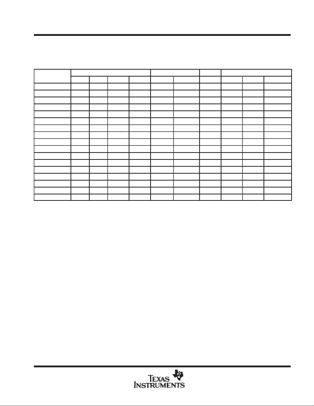
T able 1 provides an overview of ′C1x processors with comparisons of memory , I/O, cycle timing, military support,
and package types. For specific availability, contact the nearest TI Field Sales Office.
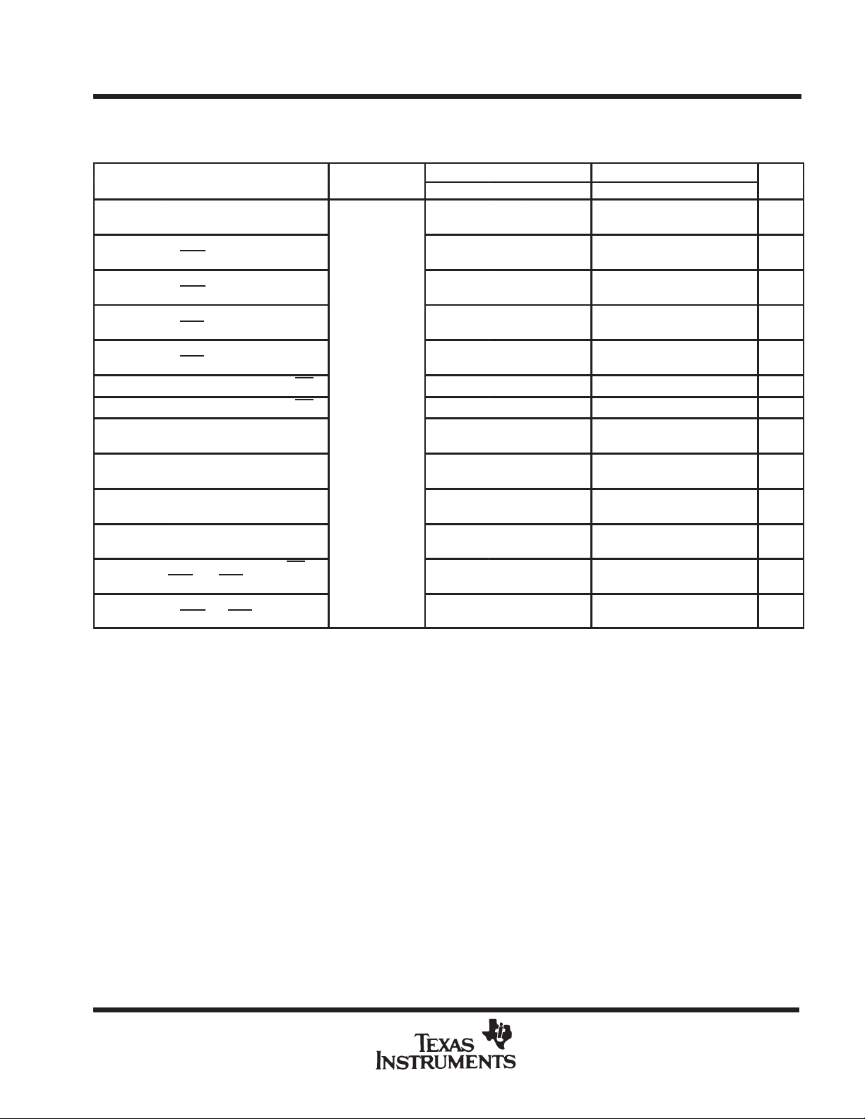
Table 1. TMS320C1x Device Overview
DEVICE
TMS320C10 (2) 144 1.5K — 4K — 8 × 16 200 40 44 —
TMS320C10-14 144 1.5K — 4K — 8 × 16 280 40 44 —
TMS320C10-25 144 1.5K — 4K — 8 × 16 160 40 44 —
TMS320C14 (3) 256 4K — 4K 1 7 × 16 (4) 160 — 68 —
TMS320E14 (3) 256 — 4K 4K 1 7 × 16 (4) 160 — — 68 CER
TMS320P14
TMS320C15 (3) 256 4K — 4K — 8 × 16 200 40 44 —
TMS320C15-25 256 4K — 4K — 8 × 16 160 40 44 —
TMS320E15 (3) 256 — 4K 4K — 8 × 16 200 40 — 44 CER
TMS320E15-25 256 — 4K 4K — 8 × 16 160 40 — 44 CER
TMS320LC15 256 4K — 4K — 8 × 16 250 40 44 —
TMS320P15
TMS320C16 256 8K — 64K — 8 × 16 114 — — 64 QFP
TMS320C17 256 4K — — 2 6 ×16 (5) 200 40 44 —
TMS320E17 (5) 256 — 4K — 2 6 × 16 (5) 200 40 — 44 CER
TMS320LC17 (5) 256 4K — — 2 6 × 16 (5) 278 40 44 —
TMS320P17 (5)
†
One-time programmable (OTP) device is in a windowless plastic package and cannot be erased.
NOTES: 1. DIP = dual in-line package. PLCC = plastic-leaded chip carrier. CER = ceramic-leaded chip carrier. QFP = plastic quad flat pack.
†
†
2. Military version available.
3. Military versions planned; contact nearest TI Field Sales Office for availability .
4. On-chip 16-bit I/O, four capture inputs, and six compare outputs are available.
5. On-chip 16-bit coprocessor interface is optional by pin selection.
RAM ROM EPROM PROG. SERIAL PARALLEL (ns) DIP PLCC CER-QUAD
256 — 4K 4K 1 7 × 16 (4) 160 — 68 —
256 — 4K 4K — 8 × 16 200 40 44 —
†
256 — 4K — 2 6 × 16 (5) 200 40 44
MEMORY I/O CYCLE PACKAGE (1)
2
POST OFFICE BOX 1443 • HOUSTON, TEXAS 77001

TMS320C1x
DIGITAL SIGNAL PROCESSORS
SPRS009C–JANUARY 1987–REVISED JUL Y 1991
description
TMS320C10
The ′C10 provides the core CPU used in all other ′C1x devices. Its microprocessor operates at 5 MIPS. It
provides a parallel I/O of 8 × 16 bits. Three versions with cycle times of 160, 200, and 280 ns are available as
illustrated in Table 1. The ′C10 versions are offered in plastic 40-pin DIP or a 44-lead PLCC packages.
TMS320C14/E14/P14
The ′C14/E14/P14 devices, using the ′C10 core CPU, offer expanded on-chip RAM, and ROM or EPROM
(′E14/P14), 16 pins of bit selectable parallel I/O, an I/O mapped asynchronous serial port, four 16-bit timers, and
external/internal interrupts. The ′C14 devices can provide for microcomputer/microprocessor operating modes.
Three versions with cycle times of 160-ns are available as illustrated in Table 1. These devices are offered in
68-pin plastic PLCC or ceramic CER-QUAD packages.
TMS320C15/E15/P15
The ′C15/E15/P15 devices are a version of the ′C10, offering expanded on-chip RAM, and ROM or EPROM
(′E15/P15). The ′P15 is a one-time programmable (OTP), windowless EPROM version. These devices can
operate in the microcomputer or microprocessor modes. Five versions are available with cycle times of 160 to
200 ns (see Table 1). These devices are offered in 40-pin DIP, 44-pin PLCC, or 44-pin ceramic packages.
TMS320LC15
The ′LC15 is a low-power version of the ′C15, utilizing a V
requirement reduction over the typical 5-V ′C1x device. It operates at a cycle time of 250 ns. The device is offered
in 40-pin DIP or 44-lead PLCC packages.
of only 3.3-V . This feature results in a 2.3: 1 power
DD
TMS320C16
The ′C16 offers on-chip RAM of 256-words, an expanded program memory of 64K-words, and a fast instruction
cycle time of 114 ns (8.77 MIPS). It is offered in a 64-pin quad flat-pack package.
TMS320C17/E17/P17
The ′C17/E17/P17 versions consist of five major functional units: the ′C15 microcomputer, a system control
register, a full-duplex dual channel serial port, µ-law/A-law companding hardware, and a coprocessor port. The
dual-channel serial port is capable of full-duplex serial communication and offers direct interface to two
combo-codecs. The hardware companding logic can operate in either µ-law or A-law format with either
sign-magnitude or twos complement numbers in either serial or parallel modes. The coprocessor port allows
the ′C17/E17/P17 to act as a slave microcomputer or as a master to a peripheral microcomputer .
The ′P17 utilizes a one-time programmable (OTP) windowless EPROM version of the ′E17.
TMS320LC17
The ′LC17 is a low-power version of the ′C17, utilizing a V
2.3: 1 power requirement reduction over the typical 5-V ′C1x device. It operates at a cycle time of 278 ns.
of only 3.3-V. This feature results in a
DD
POST OFFICE BOX 1443 • HOUSTON, TEXAS 77001
3
TMS320C1x
DIGITAL SIGNAL PROCESSORS
SPRS009C–JANUARY 1987– REVISED JULY 1991
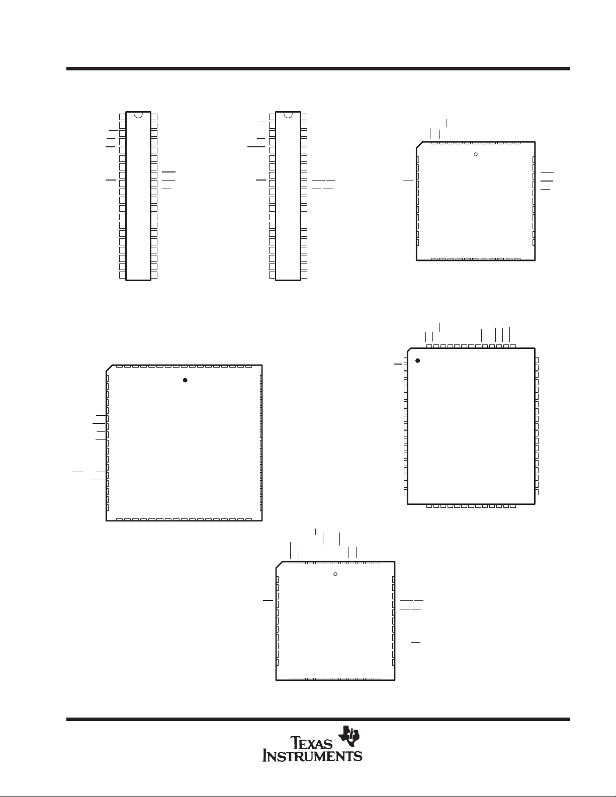
TMS320C10/C15/LC15/P15
N/JD Packages
A1/PA1
A0/PA0
MC/MP
RS
INT
CLKOUT
X1
X2/CLKIN
BIO
V
SS
D8
D9
D10
D11
D12
D13
D14
D15
D7
D6
TCLK/CLKR
TCLK2/CLKX
CLKOUT
NMI
/MC/MP
CLKIN
9876543216867666564636261
10
11
A8
12
A7
13
A6
14
WE
15
REN
16
RS
17
INT
18
19
A5
20
A4
21
22
WDT
23
24
A3
25
A2
26
27 28 29 30 31 32 33 34 35 36 37 38 39 40 41 42 43
(Top View)
40
1
39
2
38
3
37
4
36
5
35
6
34
7
33
8
32
9
31
10
30
11
29
12
28
13
27
14
26
15
25
16
24
17
23
18
22
19
21
20
TMS320C14/E14/P14
FN/FZ Packages
A9
CMP0
CMP1
A10
A11
A1
A0
IOP15
IOP14
IOP13
A2/PA2
A3
A4
A5
A6
A7
A8
MEN
DEN
WE
V
CC
A9
A10
A11
D0
D1
D2
D3
D4
D5
(Top View)
CC2VSS2
CMP2
V
CMP3
CC1VSS1
V
IOP12
D15
CAP0
D14
CAP1
IOP11
TMS320C17/E17/LC17/P17
PA1/RBLE
PA0/HI/LO
EXINT
CLKOUT
X2/CLKIN
D8/LD8
D9/LD9
D10/Ld10
D11/LD11
D12/LD12
D13/LD13
D14/LD14
D15/LD15
D7/LD7
D6/LD6
AMP4/CAP2/FSR
IOP10
D2
D0
D1
CMP5/CAP3/FSX
D13
D12
IOP9
IOP8
CLKOUT
X2/CLKIN
N/JD Packages
(Top View)
1
2
MC
3
RS
4
5
6
X1
7
8
BIO
9
V
10
SS
11
12
13
14
15
16
17
18
19
20
D3
D4
60
D5
59
D6
58
D7
57
IOP0
56
IOP1
55
IOP2
54
IOP3
53
IOP4
52
IOP5
51
D8
50
D9
49
RXD/DATA
48
TXD/CLK
47
D10
46
IOP6
45
IOP7
44
D11
X1
BIO
NC
V
SS
D8
D9
D10
D11
D12
40
PA2/TBLF
39
FSR
38
FSX
37
FR
36
DX1
35
DX0
34
SCLK
33
DR1
32
DEN
31
30
29
28
27
26
25
24
23
22
21
/RD
WE/WR
V
CC
DR0
XF
MC/PM
D0/LD0
D1/LD1
D2/LD2
D3/LD3
D4/LD4
D5/LD5
TMS320C17/E17
FN/FZ Packages
(Top View)
PAO/HI/LO
PA1/RBLE
D7/LD7
D14/LD14
D15/LD15
SS
PA2/TBLF
V
44 43 42 41 40
123456
D6/LD6
D5/LD5
EXINTRSMC
7
8
9
10
11
12
13
14
15
16
17
18 19 20 21 22 23 24 25 26 27 28
SS
V
D13/LD13
FSR
FSXFRDX1
D4/LD4
D3/LD3
X2/CLKIN
X2/CLKIN
CLKOUT
39
38
37
36
35
34
33
32
31
30
29
D2/LD2
D1/LD1
TMS320C10/C15/E15/LC15/P15
FN/FZ Packages
(Top View)
INTRSMC/MP
CLKOUT
BIO
NC
V
D10
D11
D12
7
X1
8
9
10
11
12
SS
13
D8
D9
14
15
16
17
18 19 20 21 22 23 24 25 26 27 28
CC
D13
V
TMS320C16
PG Package
(Top View)
SS
BIO
INT
V
MC/MP
64636261605958575655545352
1
NC
2
RS
3
X1
4
5
V
SS
6
V
SS
7
V
SS
8
V
SS
9
10
D15
11
D14
12
NC
13
D13
14
D12
15
D11
16
D10
17
D9
NC
18
NC
19
20212223242526272829303132
D8D7D6D5D4D3D2NCD1
DX0
SCLK
DR1
/RD
DEN
WE/WR
V
CC
DR0
XF
MC/PM
D0/LD0
V
SS
D14
V
A0/PA0
D15
DDDDDD
DD
VVV
NC
A1/PA1
CC
A2/PA2A3A4A5A6
V
44 43 42 41 40
123456
D7D6D5
MEN
DD
V
NC
D4
D3
IOEN
D2
MWE
IOWE
D0
A15
39
A7
38
A8
37
MEN
36
DEN
35
WE
34
V
CC
33
A9
32
A10
31
A11
30
D0
29
D1
CC
V
51
NC
50
NC
A0/PA0
49
A1/PA1
48
A2/PA2
47
46
A3
A4
45
44
A5
43
A6
V
42
SS
A7
41
A8
40
A9
39
A10
38
A11
37
A12
36
35
A13
34
A14
33
NC
4
POST OFFICE BOX 1443 • HOUSTON, TEXAS 77001

TMS320C1x
DIGITAL SIGNAL PROCESSORS
SPRS009C–JANUARY 1987–REVISED JUL Y 1991
architecture
The ′C1x DSPs use a modified Harvard architecture for speed and flexibility. In a strict Harvard architecture,
program and data memory lie in two separate spaces, permitting a full overlap of instruction fetch and one-cycle
execution. The ′C1x DSPs modification allows transfers between program and data spaces, thereby increasing
the flexibility of the device. This modification permits coefficients stored in program memory to be read into the
RAM, eliminating the need for a separate coefficient ROM.
32-bit accumulator
All ′C1x devices contain a 32-bit ALU and accumulator for support of double-precision, twos-complement
arithmetic. The ALU is a general-purpose arithmetic unit that operates on 16-bit words taken from the data RAM
or derived from immediate instructions. In addition to the usual arithmetic instructions, the ALU can perform
Boolean operations, providing the bit manipulation ability required of a high-speed controller. The accumulator
stores the output from the ALU and is often an input to the ALU. It operates with a 32-bit word length. The
accumulator is divided into a high-order word (bits 31 through 16) and a low-order word (bits 15 through 0).
Instructions are provided for storing the high- and low-order accumulator words in memory.
shifters
Two shifters are available for manipulating data. The ALU barrel shifter performs a left-shift of 0 to 16 places
on data memory words loaded into the ALU. This shifter extends the high-order bit of the data word and zero-fills
the low-order bits for twos-complement arithmetic. The accumulator parallel shifter performs a left-shift of 0, 1
or 4 places on the entire accumulator and places the resulting high-order accumulator bits into data RAM. Both
shifters are useful for scaling and bit extraction.
16 × 16-bit parallel multiplier
The multiplier performs a 16 × 16-bit twos-complement multiplication with a 32-bit result in a single instruction
cycle. The multiplier consists of three units: the T Register, P Register, and a multiplier array. The 16-bit T
Register stores the multiplicand, and the P Register stores the 32-bit product. Multiplier values either come from
the data memory or are derived immediately from the MPYK (multiply immediate) instruction word. The fast
on-chip multiplier allows the device to perform fundamental operations such as convolution, correlation, and
filtering.
data and program memory
Since the ′C1x devices use a Harvard type architecture, data and program memory reside in two separate
spaces. These DSP devices have 144-or 256-words of on-chip data RAM and 1.5K- to 8K-words of on-chip
program ROM. On-chip program EPROM of 4K-words is provided in the ′E14/E15/E17 devices. An on-chip
one-time programmable 4K-word EPROM is provided in the ′P14/P15/P17 devices. The EPROM cell utilizes
standard PROM programmers and is programmed identically to a 64K CMOS EPROM (TMS27C64).
(Reference Table 1.)
program memory expansion
All ′C1x devices except the ′C17/E17/LC17/P17 devices are capable of executing from off-chip external memory
at full speed for those applications requiring external program memory space. This allows for external
RAM-based systems to provide multiple functionality. The ′C17/E17/LC17/P17 devices provide no external
memory expansion. (Reference Table 1.)
microcomputer/microprocessor operating modes
All devices except the ′x17 offer two modes of operation defined by the state of the MC/MP
microcomputer mode (MC/MP = 1) or the microprocessor mode (MC/MP = 0 ). In the microcomputer mode,
on-chip ROM is mapped into the program memory space. In the microprocessor mode, all words of progam
memory are external.
pin: the
POST OFFICE BOX 1443 • HOUSTON, TEXAS 77001
5

TMS320C1x
DIGITAL SIGNAL PROCESSORS
SPRS009C–JANUARY 1987– REVISED JULY 1991
interrupts and subroutines
All devices except the ′C16 contain a four-level stack for saving the contents of the program counter during
interrupts and subroutine calls. Because of the larger 64K program space, the ′C16’s hardware stack has been
increased to eight levels. Instructions are available for saving the device’s complete context. PUSH and POP
instructions permit a level of nesting restricted only by the amount of available RAM. The interrupts used in these
devices are maskable.
input/output
The 16-bit parallel data bus can be utilized to perform I/O functions in two cycles. The I/O ports are addressed
by the three LSBs on the address lines. In addition, a polling input for bit test and jump operations (BIO
an interrupt pin (INT) have been incorporated for multitasking. The bit selectable I/O of the ′C14 is suitable for
microcontroller applications.
serial port (TMS320C17/E17)
Two of the I/O ports on the ′C17/E17 are dedicated to the serial port and companding hardware. I/O port 0 is
dedicated to control register 0, which controls the serial port, interrupts, and companding hardware. I/O port 1
accesses control register 1, as well as both serial port channels, and companding hardware. The six remaining
I/O ports are available for external parallel interfaces.
serial port (TMS320C14/E14)
The ′C14/E14 devices include one I/O-mapped serial port that operates asynchronously. I/O-mapped control
registers are used to configure port parameters such as inter-processor communication protocols and baud
rate.
) and
companding hardware (TMS320C17/E17)
On-chip hardware enables the ′C17/E17 to compand (COMpress/exP AND) data in either µ-law or A-law format.
The companding logic operation is configured via the system control register. Data may be companded in either
serial mode for operation on serial port data (converting between linear and logarithmic PCM) or a parallel mode
for computation inside the device. The ′C17/E17 allows the hardware companding logic to operate with either
sign-magnitude or twos-complement numbers.
coprocessor port (TMS320C17/E17)
The coprocessor port on the ′C17/E17 provides a direct connection to most microcomputers and
microprocessors. The port is accessed through I/O port 5 using IN and OUT instructions. The coprocessor
interface allows the device to act as a peripheral (slave) microcomputer to a microprocessor, or as a master to
a peripheral microcomputer. In the microcomputer mode, the 16 data lines are used for the 6 parallel 16-bit I/O
ports. In the coprocessor mode, the 16-bit parallel port is reconfigured to operate as a 16-bit latched bus
interface. For peripheral transfer, an 8-bit or 16-bit length of the coprocessor port can be selected.
6
POST OFFICE BOX 1443 • HOUSTON, TEXAS 77001
TMS320C1x
DIGITAL SIGNAL PROCESSORS
SPRS009C–JANUARY 1987–REVISED JUL Y 1991
instruction set
A comprehensive instruction set supports both numeric-intensive operations, such as signal processing, and
general-purpose operations, such as high-speed control. All of the ′C1x devices are object-code compatible and
use the same 60 instructions. The instruction set consists primarily of single-cycle single-word instructions,
permitting execution rates of more than six million instructions per second. Only infrequently used branch and
I/O instructions are multicycle. Instructions that shift data as part of an arithmetic operation execute in a single
cycle and are useful for scaling data in parallel with other operations.
NOTE
The BIO pin on other ′C1x devices is not available for use in the ′C14/E14/P14. An attempt to execute the
BIOZ (Branch on BIO
Three main addressing modes are available with the instruction set: direct, indirect, and immediate addressing.
direct addressing
In direct addressing, seven bits of the instruction word concatenated with the 1-bit data page pointer form the
data memory address. This implements a paging scheme in which the first page contains 128 words, and the
second page contains up to 128 words.
indirect addressing
Indirect addressing forms the data memory address from the least-significant eight bits of one of the two auxiliary
registers, AR0-AR1. The Auxiliary Register Pointer (ARP) selects the current auxiliary register. The auxiliary
registers can be automatically incremented or decremented and the ARP changed in parallel with the execution
of any indirect instruction to permit single-cycle manipulation of data tables. Indirect addressing can be used
with all instructions requiring data operands, except for the immediate operand instructions.
low) instruction will result in a two cycle NOP action.
immediate addressing
Immediate instructions derive data from part of the instruction word rather than from the data RAM. Some useful
immediate instructions are multiply immediate (MPYK), load accumulator immediate (LACK), and load auxiliary
register immediate (LARK).
instruction set summary
T able 2 lists the symbols and abbreviations used in T able 3, the instruction set summary . T able 3 contains a short
description and the opcode for each ′C1x instruction. The summary is arranged according to function and
alphabetized within each functional group.
Table 2. Instruction Symbols
SYMBOL MEANING
ACC Accumulator
D Data memory address field
M Addressing mode bit
K Immediate operand field
PA 3-bit port address field
R 1-bit operand field specifying auxiliary register
S 4-bit left-shift code
X 3-bit accumulator left-shift field
POST OFFICE BOX 1443 • HOUSTON, TEXAS 77001
7
TMS320C1x
DIGITAL SIGNAL PROCESSORS
SPRS009C–JANUARY 1987– REVISED JULY 1991
Table 3. TMS320C1x Instruction Set Summary
ACCUMULATOR INSTRUCTIONS
MNEMONIC DESCRIPTION INSTRUCTION REGISTER
ABS Absolute value of accumulator 1 1 0 1 1 1 1 1 1 1 1 0 0 0 1 0 0 0
ADD Add to accumulator with shift 1 1 0 000 M
ADDH Add to high-order accumulator bits 1 1 0 1100000M
ADDS Add to accumulator with no sign extension 1 1 0 1100001M
AND AND with accumulator 1 1 0 1111001M
LAC Load accumulator with shift 1 1 0 010 M
LACK Load accumulator immediate 1 1 0 1111110
OR OR with accumulator 1 1 0 1111010M
SACH Store high-order accumulator bits with shift 1 1 0 1011 M
SACL Store low-order accumulator bits 1 1 0 1010000M
SUB Subtract from accumulator with shift 1 1 0 001 M
SUBC Conditional subtract (for divide) 1 1 0 1100100M
SUBH Subtract from high-order accumulator bits 1 1 0 1100010M
SUBS Subtract from accumulator with no sign extension 1 1 0 1100011M
XOR Exclusive OR with accumulator 1 1 0 1111000M
ZAC Zero accumulator 1 1 0 111111110001001
ZALH Zero accumulator and load high-order bits 1 1 0 1100101M
ZALS Zero accumulator and load low-order bits with no sign extension 1 1 0 1100110M
AUXILIARY REGISTER AND DATA PAGE POINTER INSTRUCTIONS
MNEMONIC DESCRIPTION INSTRUCTION REGISTER
LAR Load auxiliary register 1 1 0 0 1 1 1 0 0 R M
LARK Load auxiliary register immediate 1 1 0 111000R
LARP Load auxiliary register pointer immediate 1 1 0 11010001000000K
LDP Load data memory page pointer 1 1 0 1101111M
LDPK Load data memory page pointer immediate 1 1 0 11011100000000K
MAR Modify auxiliary register and pointer 1 1 0 1101000M
SAR Store auxiliary register 1 1 0 0 1 1 0 0 0 R M
NO.
CYCLES
NO.
CYCLES
NO.
WORDS
15 14 13 12 11 10 9 8 7 6 5 4 3 2 1 0
NO.
WORDS
15 14 13 12 11 10 9 8 7 6 5 4 3 2 1 0
OPCODE
S
S
X
S
OPCODE
D
D
D
D
D
K
D
D
D
D
D
D
D
D
D
D
D
K
D
D
D
8
POST OFFICE BOX 1443 • HOUSTON, TEXAS 77001
TMS320C1x
DIGITAL SIGNAL PROCESSORS
SPRS009C–JANUARY 1987–REVISED JUL Y 1991
Table 3. TMS320C1x Instruction Set Summary (continued)
BRANCH INSTRUCTIONS
MNEMONIC DESCRIPTION INSTRUCTION REGISTER
B Branch unconditionally 2 2
BANZ Branch on auxiliary register not zero 2 2
BGEZ Branch if accumulator
BGZ Branch if accumulator > 0 2 2
BIOZ Branch on BIO
BLEZ Branch if accumulator
BLZ Branch if accumulator < 0 2 2
BNZ Branch if accumulator ≠ 022
BV Branch on overflow 2 2
BZ Branch if accumulator = 0 2 2
CALA Call subroutine from accumulator
CALL Call subroutine immediately 2 2
RET Return from subroutine or interrupt routine
MNEMONIC DESCRIPTION INSTRUCTION REGISTER
APAC Add P register to accumulator 1 1 0 1 1 1 1 1 1 1 1 0 0 0 1 1 1 1
LT Load T Register 1 1 0 1101010M
LTA LTA combines LT and APAC into one instruction 1 1 0 1101100M
LTD LTD combines LT, APAC, and DMOV into one instruction 1 1 0 1101011M
MPY Multiply with T register, store product in P register 1 1 0 1101101M
MPYK
PAC Load accumulator from P register 1 1 0 111111110001110
SPAC Subtract P register from accumulator 1 1 0 1 1 1 1 1 1 1 1 0 0 1 0 0 0 0
†
This instruction is a NOP on the ′320C14/E14/P14.
Multiply T register with immediate operand; store product
in P register
≥ 022
†
= 0
≤ 0 2 2
T REGISTER, P REGISTER, AND MULTIPLY INSTRUCTIONS
NO.
CYCLES
22
2 1 0 111111110001100
2 1 0 111111110001101
NO.
CYCLES
1 1 1 00
NO.
WORDS
15 14 13 12 11 10 9 8 7 6 5 4 3 2 1 0
1 1 1 1 1 0 0 1 0 0 0 0 0 0 0 0
0 000
1 111010000000000
0 000
1 111110100000000
0 000
1 111110000000000
0 000
1 111011000000000
0 000
1 111101100000000
0 000
1 111101000000000
0 000
1 111111000000000
0 000
1 111010100000000
0 000
1 111111100000000
0 000
1 111100000000000
0 000
NO.
WORDS
15 14 13 12 11 10 9 8 7 6 5 4 3 2 1 0
OPCODE
BRANCH ADDRESS
BRANCH ADDRESS
BRANCH ADDRESS
BRANCH ADDRESS
BRANCH ADDRESS
BRANCH ADDRESS
BRANCH ADDRESS
BRANCH ADDRESS
BRANCH ADDRESS
BRANCH ADDRESS
BRANCH ADDRESS
OPCODE
D
D
D
D
K
POST OFFICE BOX 1443 • HOUSTON, TEXAS 77001
9
TMS320C1x
DIGITAL SIGNAL PROCESSORS
SPRS009C–JANUARY 1987– REVISED JULY 1991
Table 3. TMS320C1x Instruction Set Summary (concluded)
CONTROL INSTRUCTIONS
MNEMONIC DESCRIPTION INSTRUCTION REGISTER
DINT Disable interrupt 1 1 0 1 1 1 1 1 1 1 1 0 0 0 0 0 0 1
EINT Enable interrupt 1 1 0 111111110000010
LST Load status register 1 1 0 1111011M
NOP No operation 1 1 0 111111110000000
POP POP stack to accumulator 2 1 0 111111110011101
PUSH PUSH stack from accumulator 2 1 0 111111110011100
ROVM Reset overflow mode 1 1 0 111111110001010
SOVM Set overflow mode 1 1 0 111111110001011
SST Store status register 1 1 0 1111100M
I/O AND DATA MEMORY OPERATIONS
MNEMONIC DESCRIPTION INSTRUCTION REGISTER
DMOV Copy contents of data memory location into next higher location 1 1 0 1 1 0 1 0 0 1 M
IN Input data from port 2 1 0 1000 M
OUT Output data to port 2 1 0 1001 M
TBLR Table read from program memory to data RAM 3 1 0 1100111M
TBLW Table write from data RAM to program memory 3 1 0 1 1 1 1 1 0 1 M
NO.
CYCLES
NO.
CYCLES
NO.
WORDS
NO.
WORDS
15 14 13 12 11 10 9 8 7 6 5 4 3 2 1 0
15 14 13 12 11 10 9 8 7 6 5 4 3 2 1 0
OPCODE
OPCODE
PA
D
D
D
D
DPA
D
D
10
POST OFFICE BOX 1443 • HOUSTON, TEXAS 77001
TMS320C10, TMS320C10-14, TMS320C10-25
DIGITAL SIGNAL PROCESSORS
SPRS009C–JANUARY 1987–REVISED JUL Y 1991
Key Features: TMS320C10
• Instruction Cycle Timing
— 160-ns (TMS320C10-25)
— 200-ns (TMS32010)
— 280-ns (TMS320C10-14)
• 144 Words of On-Chip Data RAM
• 1.5K Words On-Chip Program ROM
• External Memory Expansion up to 4K
Words at Full Speed
• 16 × 16-Bit Multiplier With 32-Bit Product
• 0 to 16-Bit Barrel Shifter
• On-Chip Clock Oscillator
• Device Packaging:
— 40-Pin DIP
— 44-Lead PLCC
• Single 5-V Supply
• Operating Free-Air Temperature Range
...0°C to 70°C
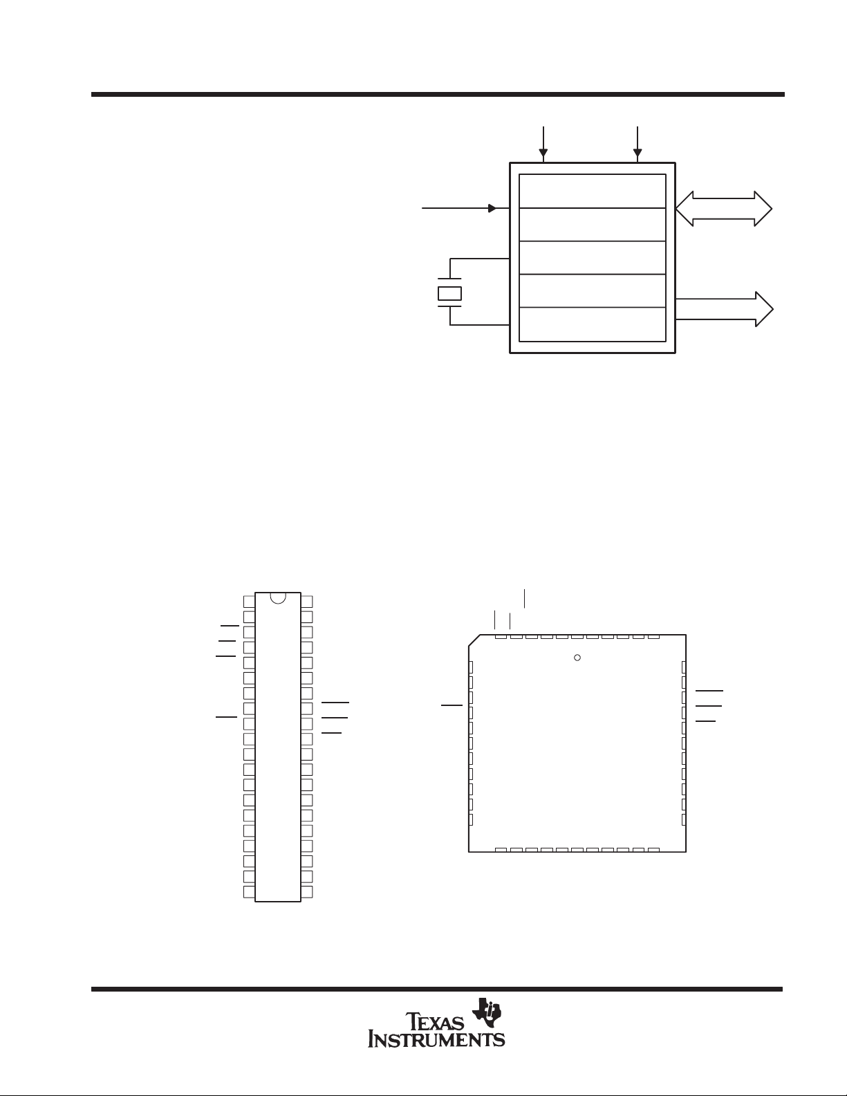
Interrupt
+5 V GND
144-Word RAM
Data (16)
1.5K-Word ROM
32-Bit ALU/ACC
Multiplier
Address (12)
Shifters
A1/PA1
A0/PA0
MC/MP
RS
INT
CLKOUT
X1
X2/CLKIN
BIO
V
SS
D8
D9
D10
D11
D12
D13
D14
D15
D7
D6
TMS320C10
N/JD Package
40
1
39
2
38
3
37
4
36
5
35
6
34
7
33
8
32
9
31
10
30
11
29
12
28
13
27
14
26
15
25
16
24
17
23
18
22
19
20
21
A2/PA2
A3
A4
A5
A6
A7
A8
MEN
DEN
WE
V
CC
A9
A10
A11
D0
D1
D2
D3
D4
D5
CLKOUT
X1
X2/CLKIN
BIO
NC
V
SS
D8
D9
D10
D11
D12
INTRSMC/MP
7
8
9
10
11
12
13
14
15
16
17
18 19 20
CC
V
TMS320C10
FN/FZ Package
(Top View)(Top View)
A0/PA0
A1/PA1
123456
21 22 23 24 25 26
D13
D7D6D5D4D3
D14
D15
SS
A2/PA2A3A4A5A6
V
44 43 42 41 40
27 28
D2
CC
V
39
38
37
36
35
34
33
32
31
30
29
A7
A8
MEN
DEN
WE
V
CC
A9
A10
A11
D0
D1
POST OFFICE BOX 1443 • HOUSTON, TEXAS 77001
11
TMS320C10, TMS320C10-14, TMS320C10-25
DIGITAL SIGNAL PROCESSORS
SPRS009C–JANUARY 1987– REVISED JULY 1991
TERMINAL FUNCTIONS
NAME I/O
A11-A0/PA2-PA0
BIO
CLKOUT
D15-D0
DEN
INT
MC/MP
MEN
NC
RS
V
CC
V
SS
WE
X1
X2/CLKIN
†
Input/Output/High-impedance state.
†
O
External address bus. I/O port address multiplexed over PA2-PA0.
I
External polling input
O
System clock output, 1/4 crystal/CLKIN frequency
I/O
16-bit parallel data bus
O
Data enable for device input data on D15-D0
I
External interrupt input
I
Memory mode select pin. High selects microcomputer mode. Low selects microprocessor mode.
O
Memory enable indicates that D15-D0 will accept external memory instruction.
O
No connection
I
Reset for initializing the device
I
+ 5 V supply
I
Ground
O
Write enable for device output data on D15-D0
O
Crystal output for internal oscillator
I
Crystal input internal oscillator or external system clock input
DEFINITION
12
POST OFFICE BOX 1443 • HOUSTON, TEXAS 77001
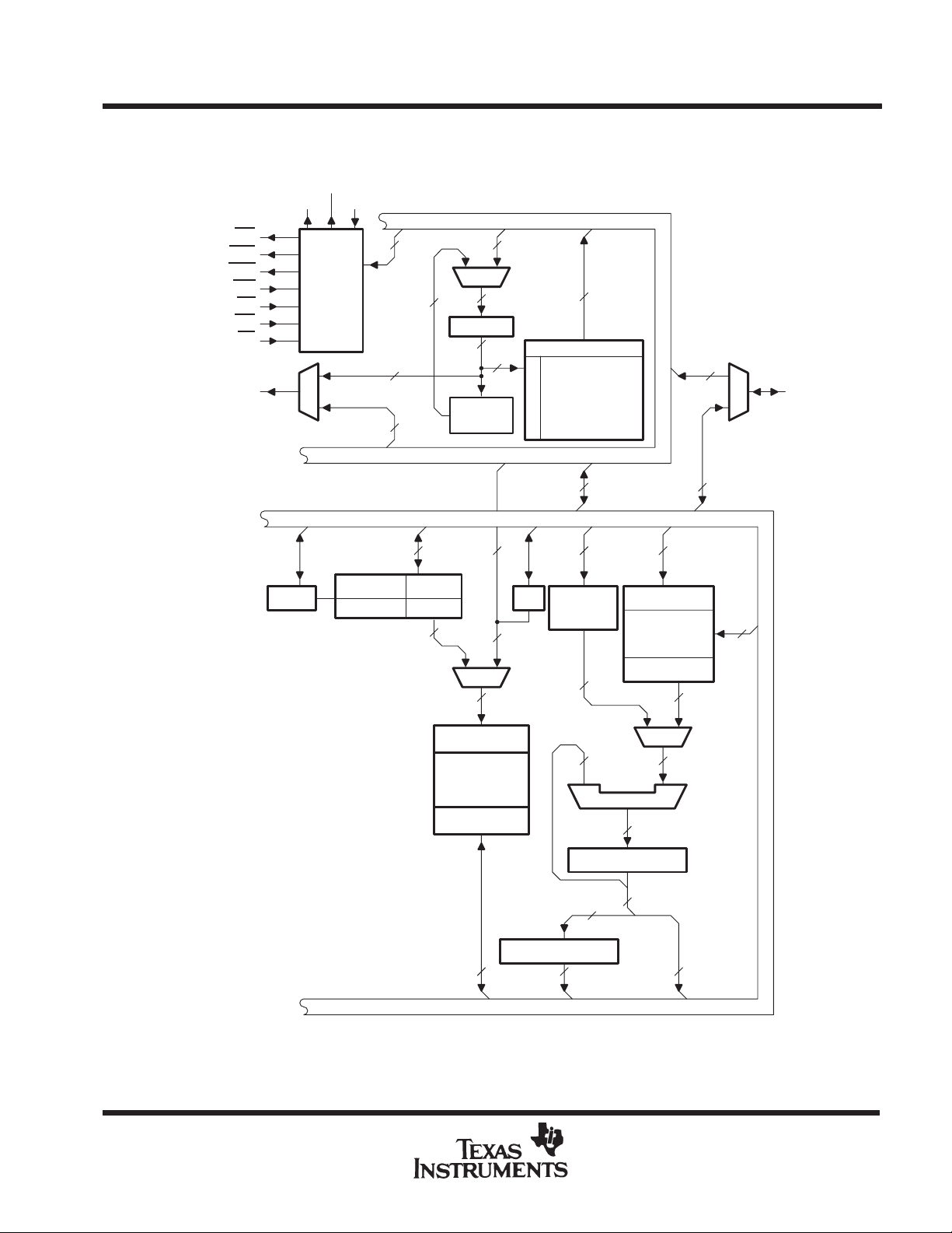
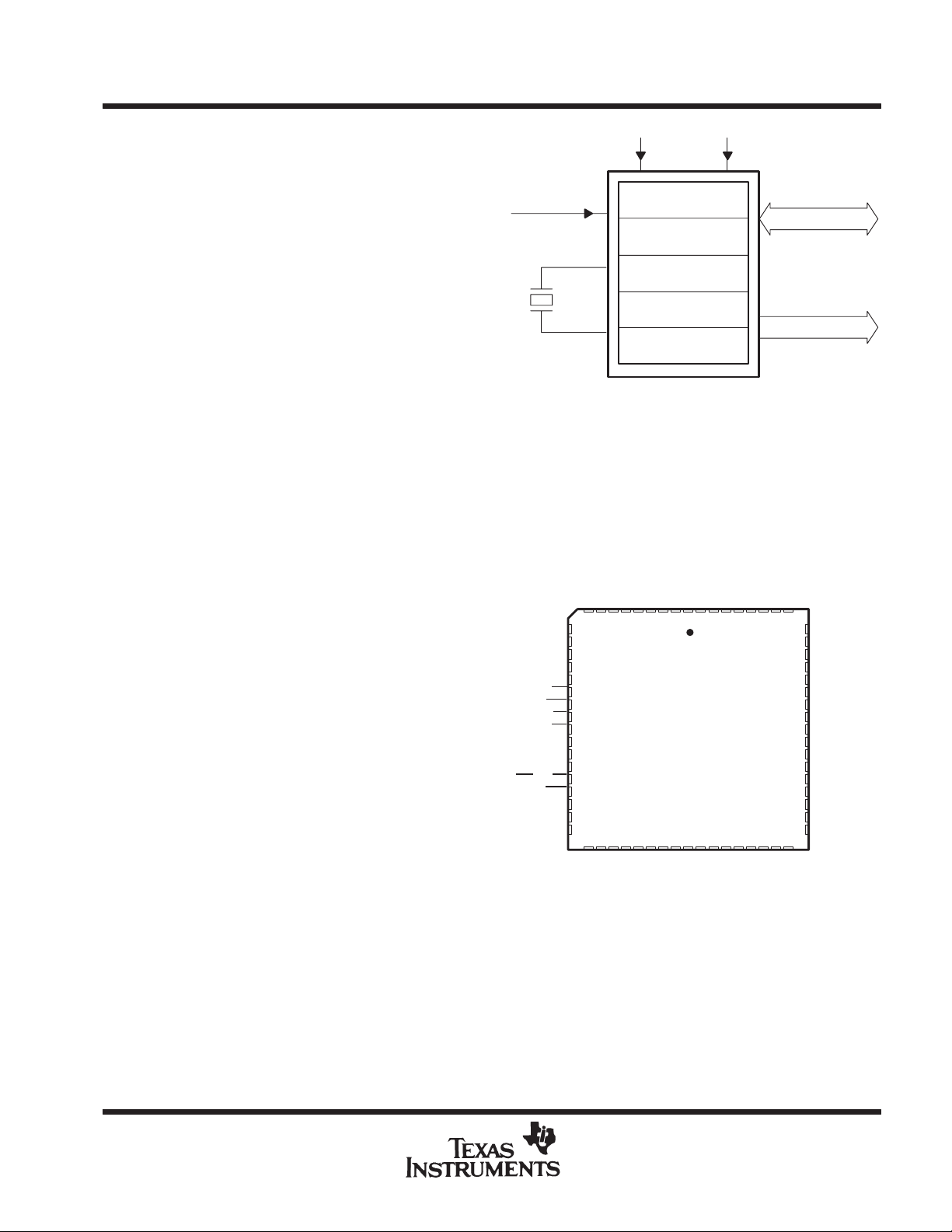
functional block diagram
WE
DEN
MEN
BIO
MC/MP
INT
RS
A11-A0/
PA2-PA0
X1
Controller
MUX
TMS320C10, TMS320C10-14, TMS320C10-25
DIGITAL SIGNAL PROCESSORS
SPRS009C–JANUARY 1987–REVISED JUL Y 1991
X2/CLKINCLKOUT
Program Bus
16
3
3
12 LSB
MUX
12
12
PC (12)
12
Stack
4 × 12
Program Bus
12
12
Instruction
Program
ROM/EPROM
(1.5K Words)
Address
16
MUX
D15-D0
ARP
Legend:
ACC = Accumulator
ALU = Arithmetic Logic Unit
ARP = Auxiliary Register Pointer
AR0 = Auxiliary Register 0
AR1 = Auxiliary Register 1
DP = Data Page Pointer
P = P Register
PC = Program Counter
T = T Register
AR0 (16)
AR1 (16)
16
8
MUX
8
Address
Data RAM
(144 Words)
Data
16 16
Data Bus
7
8
16
16
DP
Shifter
(0–16)
32
32
32
Shifter (0,1,4)
ALU (32)
32
ACC (32)
32
16
16
T(16)
Multiplier
P(32)
32
MUX
32
16
16
Data Bus
POST OFFICE BOX 1443 • HOUSTON, TEXAS 77001
13
TMS320C10, TMS320C10-14, TMS320C10-25
DIGITAL SIGNAL PROCESSORS
SPRS009C–JANUARY 1987– REVISED JULY 1991
electrical specifications
This section contains the electrical specifications for all speed versions of the ′C10 Digital Signal Processors,
including test parameter measurement information.
absolute maximum ratings over operating free-air temperature range (unless otherwise noted)
Supply voltage range VCC (see Note 6) –0.3 V to 7 V. . . . . . . . . . . . . . . . . . . . . . . . . . . . . . . . . . . . . . . . . . . . . . .
Input voltage range –0.3 V to 7 V. . . . . . . . . . . . . . . . . . . . . . . . . . . . . . . . . . . . . . . . . . . . . . . . . . . . . . . . . . . . . . . .
Output voltage range –0.3 V to 7 V. . . . . . . . . . . . . . . . . . . . . . . . . . . . . . . . . . . . . . . . . . . . . . . . . . . . . . . . . . . . . . .
Continuous power dissipation 0.5 mW. . . . . . . . . . . . . . . . . . . . . . . . . . . . . . . . . . . . . . . . . . . . . . . . . . . . . . . . . . . .
Operating free-air temperature: L suffix 0°C to 70°C. . . . . . . . . . . . . . . . . . . . . . . . . . . . . . . . . . . . . . . . . . . . . . . .
A suffix – 40°C to 85°C. . . . . . . . . . . . . . . . . . . . . . . . . . . . . . . . . . . . . . . . . . . . .
Storage temperature –55
†
Stresses beyond those listed under “Absolute Maximum Ratings” may cause permanent damage to the device. This is a stress rating only, and
functional operation of the device at these or any other conditions beyond those indicated in the “Recommended Operating Conditions” section of
this specification is not implied. Exposure to absolute-maximum-rated conditions for extended periods may affect device reliability .
NOTE 6: All voltage values are with respect to V
SS.
recommended operating conditions
MIN NOM MAX UNIT
V
Supply voltage 4.5 5 5.25 V
CC
V
Supply voltage 0 V
SS
High-level input voltage
V
IH
Low-level input voltage
V
IL
I
High-level output current, all outputs –300 µA
OH
I
Low-level output current 2 mA
OL
Operating free-air temperature
T
A
CLKIN 3 V
All remaining inputs 2 V
MC/MP 0.6 V
All remaining inputs 0.8 V
L suffix 0 70 °C
A suffix – 40 85 °C
°
C to 150 °C. . . . . . . . . . . . . . . . . . . . . . . . . . . . . . . . . . . . . . . . . . . . . . . . . . . . . . . . . . . .
†
14
POST OFFICE BOX 1443 • HOUSTON, TEXAS 77001
TMS320C10, TMS320C10-14, TMS320C10-25
DIGITAL SIGNAL PROCESSORS
SPRS009C–JANUARY 1987–REVISED JUL Y 1991
electrical characteristics over specified temperature range (unless otherwise noted)
PARAMETER TEST CONDITIONS MIN TYP
V
High-level output voltage
OH
V
Low-level output voltage IOL = MAX 0.3 0.5 V
OL
I
Off-state output current
OZ
I
Input current
I
C
Input capacitance
i
C
o Output capacitance
†
All typical values are at VCC = 5 V, TA = 25°C.
‡
Values derived from characterization data and not tested.
NOTE 7: This voltage specification is included for interface to HC logic. However, note that all of the other timing parameters defined in this data
sheet are specified for TTL logic levels and will differ for HC logic levels.
Data bus 25
All others 15
Data bus 25
All others 10
IOH = MAX 2.4 3
IOH = 20 µA (see Note 7) VCC– 0.4
VCC = MAX
VCC = VSS to V
f = 1 MHz, all other pins 0 V
VO = 2.4 V 20
VO = 0.4 V –20
All inputs except CLKIN ±20
CC
CLKIN ±50
†
MAX UNIT
‡
‡
‡
‡
‡
V
µA
µA
pF
pF
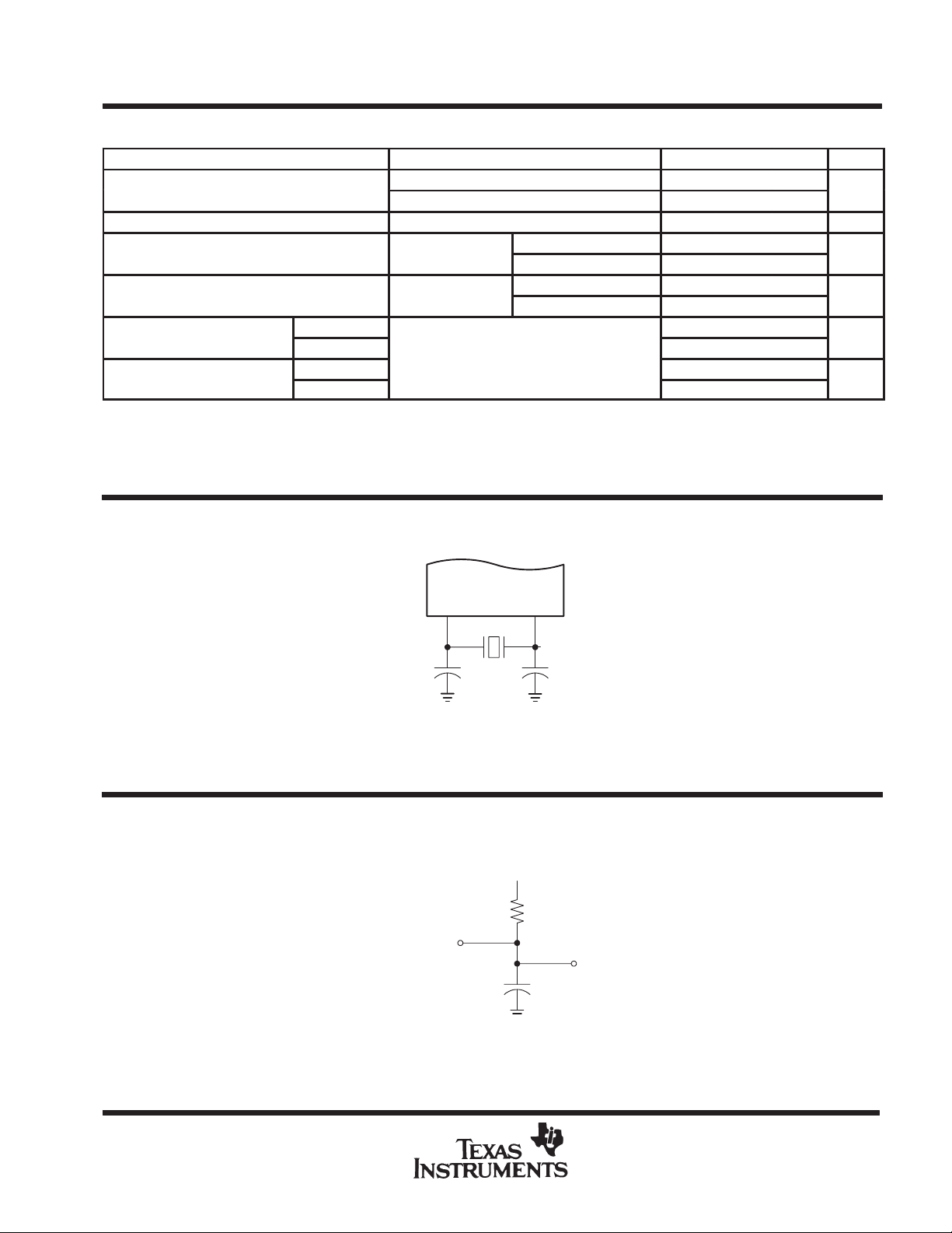
INTERNAL CLOCK OPTION
X1 X2/CLKIN
Crystal
C1 C2
Figure 1. Internal Clock Option
PARAMETER MEASUREMENT INFORMATION
2.15 V
RL = 825 Ω
From Output
Under Test
Figure 2. Test Load Circuit
Test
Point
CL = 100 pF
POST OFFICE BOX 1443 • HOUSTON, TEXAS 77001
15
TMS320C10, TMS320C10-25
DIGITAL SIGNAL PROCESSORS
SPRS009C–JANUARY 1987– REVISED JULY 1991
electrical characteristics over specified temperature range (unless otherwise noted)
PARAMETER
‡
Supply current
I
CC
†
All typical values are at TA = 70°C and are used for thermal resistance calculations.
‡
ICC characteristics are inversely proportional to temperature. For ICC dependence on temperature, frequency, and loading.
TMS320C10 f = 20.5 MHz, VCC = 5.5 V, TA = – 40°C to 85°C 33 55
TMS320C10-25 f = 25.6 MHz, VCC = 5.5 V TA = – 0°C to 70°C 40 65
CLOCK CHARACTERISTICS AND TIMING
The ′C10/C10-25 can use either its internal oscillator or an external frequency source for a clock.
internal clock option
The internal oscillator is enabled by connecting a crystal across X1 and X2/CLKIN (see Figure 1). The frequency
of CLKOUT is one-fourth the crystal fundamental frequency. The crystal should be fundamental mode, and
parallel resonant, with an effective series resistance of 30 ohms, a power dissipation of 1 mW , and should be
specified at a load capacitance of 20 pF.
PARAMETER TEST CONDITIONS MIN NOM MAX UNIT
Crystal frequency, f
C1, C2 TA = – 40°C to 85°C 10 pF
x
TMS320C10 TA = – 40°C to 85°C 6.7 20.5
TMS320C10-25 TA = 0°C to 70°C 6.7 25.6
TEST CONDITIONS
(SEE FIGURE 2)
MIN TYP†MAX UNIT
mA
MHz
external clock option
An external frequency source can be used by injecting the frequency directly into X2/CLKIN with X1 left
unconnected. The external frequency injected must conform to the specifications listed in the table below.
switching characteristics over recommended operating conditions
PARAMETER UNITTEST CONDITIONS
t
c(C)
t
r(C)
t
f(C)
t
w(CL)
t
w(CH)
t
d(MCC)
§
t
c(C)
¶
Values derived from characterization data and not tested.
CLKOUT cycle time
CLKOUT rise time 10
CLKOUT fall time 8
Pulse duration, CLKOUT low 92
Pulse duration, CLKOUT high 90
Delay time, CLKIN↑ to CLKOUT↓ 25
is the cycle time of CLKOUT, i.e., 4t
§
RL = 825 Ω,
CL = 100 pF
(see Figure 2)
(4 times CLKIN cycle time if an external oscillator is used).
c(MC)
MIN NOM MAX MIN NOM MAX
TMS320C10 TMS320C10-25
195.12 200 156.25 160 ns
¶
¶
¶
¶
¶
60
¶
25 50
10
72
70
¶
¶
8
¶
¶
timing requirements over recommended operating conditions
TMS320C10 TMS320C10-25
MIN NOM MAX MIN NOM MAX
t
c(MC)
t
r(MC)
t
f(MC)
t
w(MCP)
t
w(MCL)
t
w(MCH)
¶
Values derived from characterization data and not tested.
Master clock cycle time 48.78 50 150 39.06 40 150
Rise time, master clock input 5
Fall time, master clock input 5
Pulse duration, master clock 0.4t
Pulse duration, master clock low 20
Pulse duration, master clock high 20
c(MC)
¶
¶
¶
0.6t
¶
¶
10
10
c(MC)
¶
¶
¶
0.45t
c(MC)
¶
5
¶
5
¶
0.55t
¶
15
¶
15
10
10
c(MC)
ns
ns
ns
ns
¶
ns
UNIT
¶
ns
¶
ns
¶
ns
¶
ns
ns
ns
16
POST OFFICE BOX 1443 • HOUSTON, TEXAS 77001
DIGITAL SIGNAL PROCESSORS
SPRS009C–JANUARY 1987–REVISED JUL Y 1991
MEMORY AND PERIPHERAL INTERFACE TIMING
switching characteristics over recommended operating conditions
PARAMETER
t
d1
t
d2
t
d3
t
d4
t
d5
t
d6
t
d7
t
d8
t
d9
t
d10
t
v
t
h(A-WMD)
t
su(A-MD)
†
Values derived from characterization data and not tested.
NOTE 8: For interfacing I/O devices, see Figure 3.
Delay time, CLKOUT↓ to
address bus valid
Delay time, CLKOUT↓
to MEN
↓
Delay time, CLKOUT↓
to MEN
↑
Delay time, CLKOUT↓
to DEN
↓
Delay time, CLKOUT↓
to DEN
↑
Delay time, CLKOUT↓ to WE↓ 1/2t
Delay time, CLKOUT↓ to WE↑ –10
Delay time, CLKOUT↓ to data
bus OUT valid
Time after CLKOUT↓ that data
bus starts to be driven
Time after CLKOUT↓that data
bus stops being driven
Data bus OUT valid after
CLKOUT↓
Address hold time after WE↑,
MEN
↑, or DEN↑ (see Note 8)
Address bus setup time prior
to MEN
↓ or DEN↓
CONDITIONS
RL = 825 Ω
CL = 100 pF,
(see Figure 2)
TEST
1/4t
1/4t
1/4t
1/4t
1/4t
TMS320C10 TMS320C10-25
MIN TYP MAX MIN TYP MAX
†
10
–5†1/4t
c(C)
†
–10
†1
–5
c(C)
†
–10
–5†1/2t
c(C)
†
†
–5
c(C)
–10 1/4t
c(C)
†
–10
–45 1/4t
c(C)
1/4t
1/4t
/4t
c(C)
50 10
+15 1/4t
c(C)
15 –10
+15 1/4t
c(C)
15 –10
+ 15 1/2t
c(C)
15 –10
+ 65 1/4t
c(C)
+ 40
TMS320C10, TMS320C10-25
UNIT
†
–5†1/4t
c(C)
†
–5†1/4t
c(C)
†
†
–5
c(C)
†
1/4t
†
–10
†
–5
c(C)
–10 ns
c(C)
†
–35 ns
c(C)
1/2t
1/4t
40 ns
c(C)
12 ns
c(C)
12 ns
c(C)
12 ns
+ 52
c(C)
+ 40
c(C)
+ 12 ns
+ 12 ns
+ 12 ns
†
ns
ns
†
ns
ns
POST OFFICE BOX 1443 • HOUSTON, TEXAS 77001
17
TMS320C10, TMS320C10-25
DIGITAL SIGNAL PROCESSORS
SPRS009C–JANUARY 1987– REVISED JULY 1991
timing requirements over recommended operating conditions
TEST CONDITION
t
t
NOTE 9: Data may be removed from the data bus upon MEN↑ or DEN↑ preceding CLKOUT↓.
Setup time, data bus valid prior to CLKOUT↓ 50 40 ns
su(D)
Hold time, data bus held valid after CLKOUT↓
h(D)
(see Note 9)
RL = 825 Ω,
CL = 100 pF
(see Figure 2)
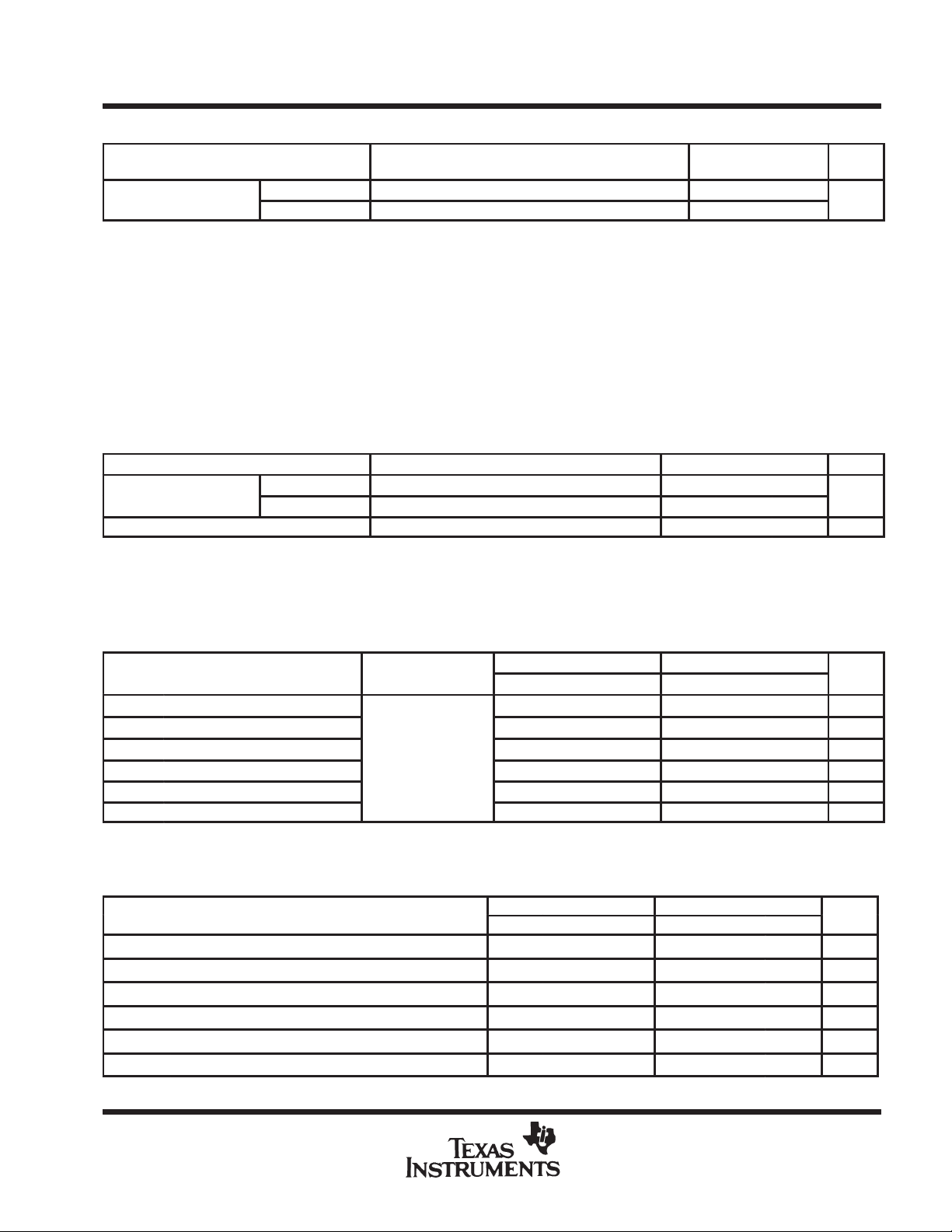
SUGGESTED I/O DECODE CIRCUIT
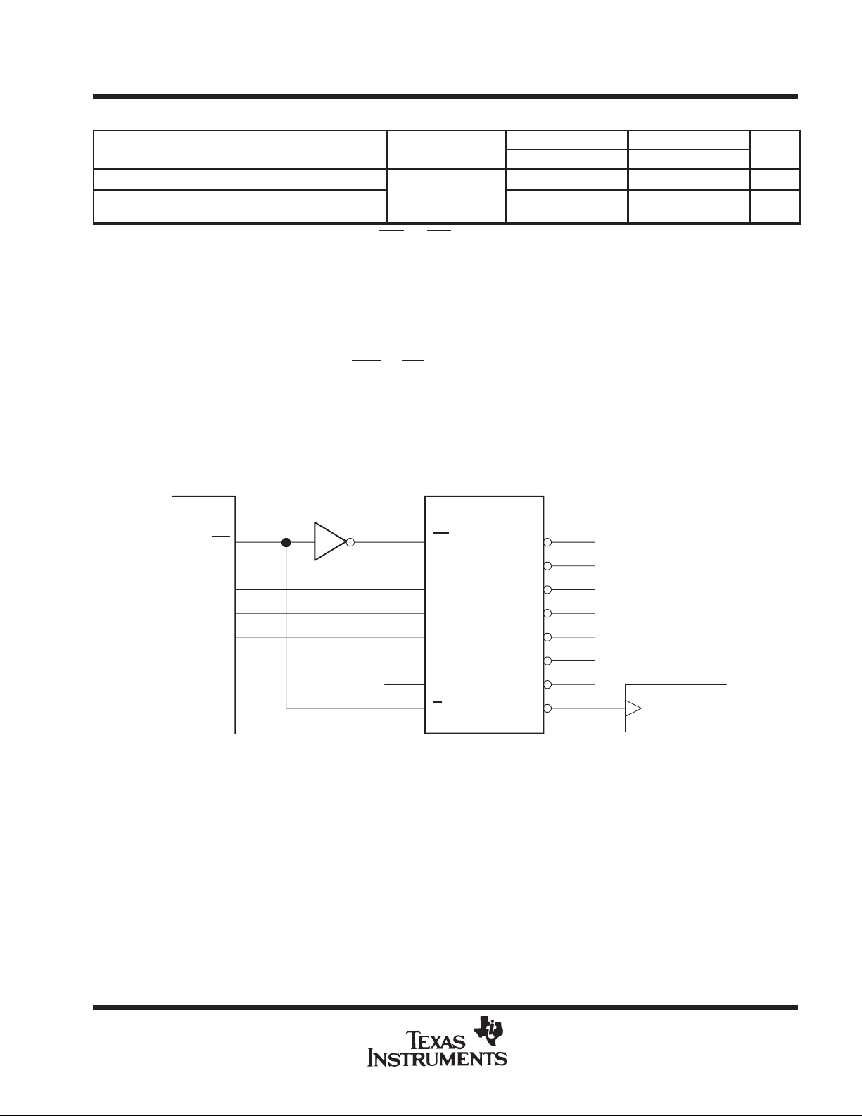
The circuit shown in Figure 3 is a design example for interfacing I/O devices to the ′C10/C10-25. This circuit
decodes the address for output operations using the OUT instruction. The same circuit can be used to decode
input and output operations if the inverter (’ALS04) is replaced with a NAND gate and both DEN and WE are
connected. Inputs and outputs can be decoded at the same port provided the output of the decoder (’AS137)
is gated with the appropriate signal (DEN
be increased when the circuit shown in Figure 3 is repeated to support IN instructions with DEN connected rather
than WE.
The table write (TBL W) function requires a dif ferent circuit. A detailed discussion of an example circuit for this
function is described in the application report, “Interfacing External Memory to the TMS32010”, published in the
book,
Digital Signal Processing Applications with the TMS320 Famil
or WE) to select read or write (using an ’ALS32). Access times can
TMS320C10 TMS320C10-25
MIN NOM MAX MIN NOM MAX
0 0 ns
y (SPRA012A).
UNIT
TMS320C10 74AS137
32
WE
2
PA0
1
PA1
40
PA2
74ALS04
4
GL
1
A
2
B
3
C
6
V
CC
G1
5
2
G
Figure 3. I/O Decode Circuit
Y0
Y1
Y2
Y3
Y4
Y5
Y6
Y7
15
14
13
12
11
10
9
7
I/O Device
18
POST OFFICE BOX 1443 • HOUSTON, TEXAS 77001
TMS320C10, TMS320C10-25
DIGITAL SIGNAL PROCESSORS
SPRS009C–JANUARY 1987–REVISED JUL Y 1991
RESET (RS) TIMING
switching characteristics over recommended operating conditions
PARAMETER TEST CONDITIONS MIN TYP MAX UNIT
t
d11
t
dis(R)
†
Values derived from characterization data and not tested.
Delay time, DEN↑, WE↑, and MEN↑ from RS 1/2t
Data bus disable time after RS
timing requirements over recommended operating conditions
PARAMETER
t
su(R)
t
w(R)
NOTE 10: RS can occur anytime during a clock cycle. Time given is minimum to ensure synchronous operation.
Reset (RS) setup time prior to CLKOUT (see Note 10) 50 40 ns
RS pulse duration 5t
INTERRUPT (INT) TIMING
RL 825 Ω,
CL = 100 pF,
(see Figure 2)
TMS320C10 TMS320C10-25
MIN NOM MAX MIN NOM MAX
c(C)
5t
c(C)
1/4t
+50† ns
c(C)
+50
c(C)
†
ns
UNIT
ns
timing requirements over recommended operating conditions
TMS320C10 TMS320C10-25
MIN NOM MAX MIN NOM MAX
t
f(INT)
t
w(INT)
t
su(INT)
Fall time, INT 15 15 ns
Pulse duration, INT t
Setup time, INT↓ before CLKOUT↓ 50 40 ns
c(C)
IO (BIO) TIMING
timing requirements over recommended operating conditions
TMS320C10 TMS320C10-25
MIN NOM MAX MIN NOM MAX
t
f(IO)
t
w(IO)
t
su(IO)
Fall time, BIO 15 15 ns
Pulse duration, BIO t
Setup time, BIO↓ before CLKOUT↓ 50 40 ns
c(C)
t
c(C)
t
c(C)
UNIT
ns
UNIT
ns
POST OFFICE BOX 1443 • HOUSTON, TEXAS 77001
19
TMS320C10-14
DIGITAL SIGNAL PROCESSORS
SPRS009C–JANUARY 1987– REVISED JULY 1991
electrical characteristics over specified temperature range (unless otherwise noted)
PARAMETER TEST CONDITIONS MIN TYP
‡
Supply current
I
CC
†
All typical values are at TA = 70°C and are used for thermal resistance calculations.
‡
ICC characteristics are inversely proportional to temperature; i.e., ICC decreases approximately linearly with temperature.
f = 14.4, MHz, VCC = 5.5 V, TA = 0°C to 70°C 28 65 mA
CLOCK CHARACTERISTICS AND TIMING
The TMS320C10-14 can use either its internal oscillator or an external frequency source for a clock.
internal clock option
The internal oscillator is enabled by connecting a crystal across X1 and X2/CLKIN (see Figure 1). The frequency
of CLKOUT is one-fourth the crystal fundamental frequency. The crystal should be fundamental mode, and
parallel resonant, with an effective series resistance of 30 ohms, a power dissipation of 1 mW , and be specified
at a load capacitance of 20 pF.
PARAMETER TEST CONDITIONS MIN NOM MAX UNIT
Crystal frequency, f
C1, C2 TA = 0°C to 70°C 10 pF
x
TA = 0°C to 70°C 6.7 14.4 MHz
†
MAX UNIT
external clock option
An external frequency source can be used by injecting the frequency directly into X2/CLKIN with X1 left
unconnected. The external frequency injected must conform to the specifications listed in the table below.
switching characteristics over recommended operating conditions
TEST CONDITIONS MIN NOM MAX UNIT
t
c(C)
t
r(C)
t
f(C)
t
w(CL)
t
w(CH)
t
d(MCC)
§t
c(C)
¶
Values derived from characterization data and not tested.
CLKOUT cycle time
CLKOUT rise time 10 ns
CLKOUT fall time 8 ns
Pulse duration, CLKOUT low 131 ns
Pulse duration, CLKOUT high 129 ns
Delay time, CLKIN↑ to CLKOUT↓ 25
is the cycle time of CLKOUT, i.e., 4t
§
RL = 825 Ω,
CL = 100 pF,
(see Figure 2)
(4 times CLKIN cycle time if an external oscillator is used).
c(MC)
277.78 ns
¶
timing requirements over recommended operating conditions
MIN NOM MAX UNIT
t
c(MC)
t
r(MC)
t
f(MC)
t
w(MCP)
t
w(MCL)
t
w(MCH)
¶
Values derived from characterization data and not tested.
Master clock cycle time 69.5 150 ns
Rise time, master clock input 5
Fall time, master clock input 5
Pulse duration, master clock 0.4t
Pulse duration, master clock low, t
Pulse duration, master clock high, t
= 50 ns 20
c(MC)
= 50 ns 20
c(MC)
c(MC)
¶
10
¶
10
¶
0.6t
c(MC)
¶
¶
60
¶
ns
¶
ns
¶
ns
¶
ns
ns
ns
20
POST OFFICE BOX 1443 • HOUSTON, TEXAS 77001
DIGITAL SIGNAL PROCESSORS
SPRS009C–JANUARY 1987–REVISED JUL Y 1991
MEMORY AND PERIPHERAL INTERFACE TIMING
switching characteristics over recommended operating conditions
PARAMETER TEST CONDITIONS MIN NOM MAX UNIT
t
d1
t
d2
t
d3
t
d4
t
d5
t
d6
t
d7
t
d8
t
d9
t
d10
t
v
t
h(A-WMD)
t
su(A-MD)
†
Values derived from characterization data and not tested.
NOTE 8: For interfacing I/O devices, see Figure 3.
Delay time, CLKOUT↓ to address bus valid 10
Delay time, CLKOUT↓ to MEN↓ 1/4t
Delay time, CLKOUT↓ to MEN↑ –10
Delay time, CLKOUT↓ to DEN↓ 1/4t
Delay time, CLKOUT↓ to DEN↑ –10
Delay time, CLKOUT↓ to WE↓ 1/2t
Delay time, CLKOUT↓ to WE↑ –10
Delay time, CLKOUT↓ to data bus OUT valid 1/4t
Time after CLKOUT↓ that data bus starts to be driven 1/4t
Time after CLKOUT↓that data bus stops being driven 1/4t
Data bus OUT valid after CLKOUT↓ 1/4t
Address hold time after WE↑, MEN↑, or DEN↑
(see Note 8)
Address bus setup time prior to MEN↓ or DEN↓ 1/4t
RL = 825 Ω,
CL = 100 pF
(see Figure 2)
TMS320C10-14
†
†
– 5
c(C)
†
†1
– 5
c(C)
†
†
– 5
c(C)
†
†
– 5
c(C)
– 10 ns
c(C)
†
–10
– 45 ns
c(C)
1/4t
/4t
1/2t
c(C)
c(C)
c(C)
c(C)
c(C)
50 ns
15 ns
15 ns
15 ns
+15 ns
+15 ns
+15 ns
+ 65 ns
ns
+ 40†ns
ns
timing requirements over recommended operating conditions
TEST CONDITIONS MIN NOM MAX UNIT
t
su(D)
t
h(D)
NOTE 9: Data may be removed from the data bus upon MEN↑ or DEN↑ preceding CLKOUT↓.
Setup time, data bus valid prior to CLKOUT↓ 50 ns
Hold time, data bus held valid after CLKOUT↓ (see Note 9) 0 ns
RL = 825 Ω,
CL = 100 pF
(see Figure 2)
POST OFFICE BOX 1443 • HOUSTON, TEXAS 77001
21
TMS320C10-14
DIGITAL SIGNAL PROCESSORS
SPRS009C–JANUARY 1987– REVISED JULY 1991
RESET (RS) TIMING
switching characteristics over recommended operating conditions
PARAMETER TEST CONDITIONS MIN TYP MAX UNIT
t
d11
t
dis(R)
†
Values were derived from characterization data and not tested.
Delay time, DEN↑, WE↑, and MEN↑ from RS 1/2t
Data bus disable time after RS
timing requirements over recommended operating conditions
t
su(R)
t
w(R)
NOTE 10: RS can occur anytime during a clock cycle. Time given is minimum to ensure synchronous operation.
Reset (RS) setup time prior to CLKOUT (see Note 10) 50 ns
RS pulse duration 5t
INTERRUPT (INT) TIMING
timing requirements over recommended operating conditions
t
f(INT)
t
w(INT)
t
su(INT)
Fall time, INT 15 ns
Pulse duration, INT t
Setup time, INT↓ before CLKOUT↓ 50 ns
RL = 825 Ω,
CL = 100 pF
(see Figure 2)
MIN NOM MAX UNIT
c(C)
MIN NOM MAX UNIT
c(C)
1/4t
c(C)
c(C)
+ 50
+ 50
†
ns
†
ns
ns
ns
IO (BIO) TIMING
timing requirements over recommended operating conditions
t
f(IO)
t
w(IO)
t
su(IO)
Fall time, BIO 15 ns
Pulse duration, BIO t
Setup time, BIO↓ before CLKOUT↓ 50 ns
MIN NOM MAX UNIT
c(C)
ns
22
POST OFFICE BOX 1443 • HOUSTON, TEXAS 77001
TMS320C10, TMS320C10-14, TMS320C10-25
DIGITAL SIGNAL PROCESSORS
SPRS009C–JANUARY 1987–REVISED JUL Y 1991
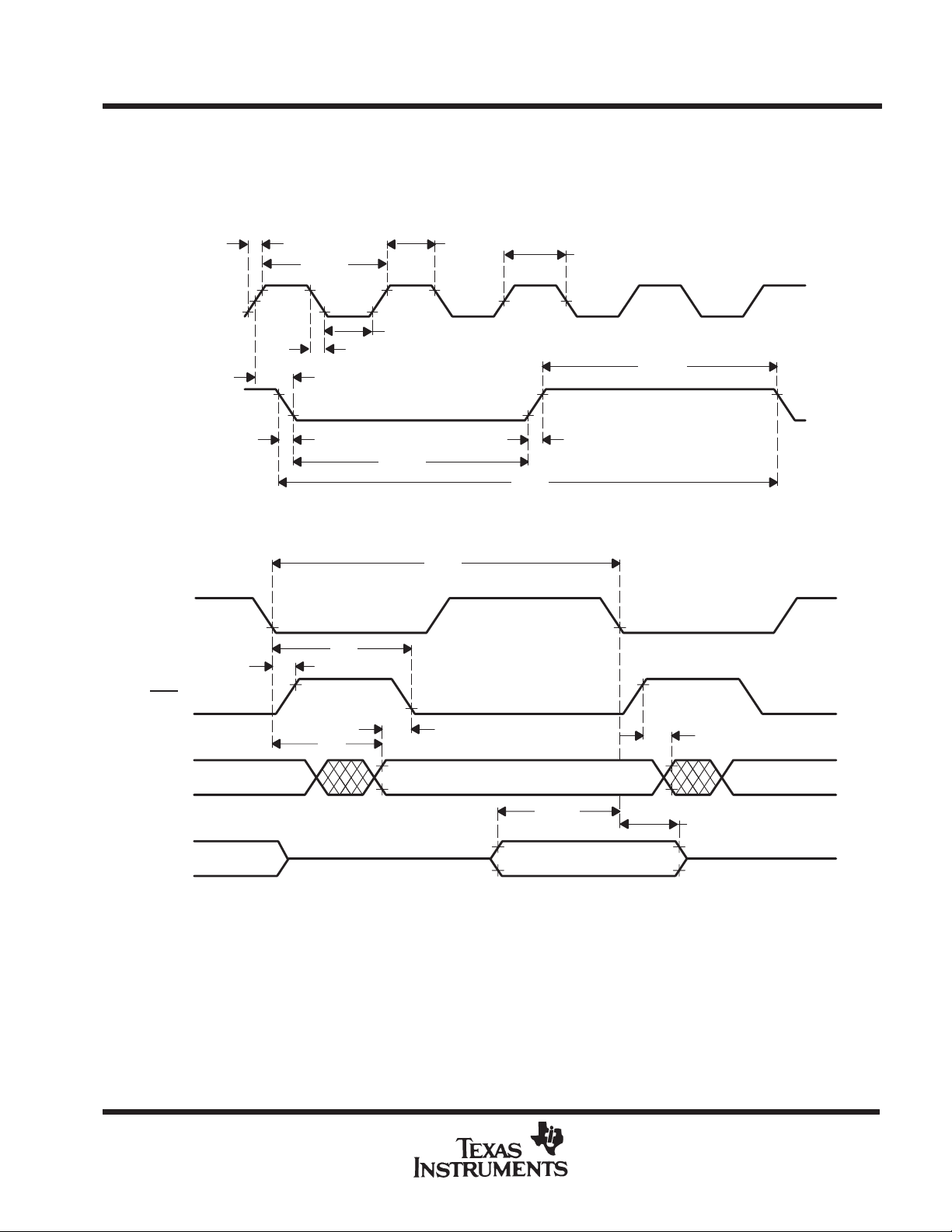
TIMING DIAGRAMS
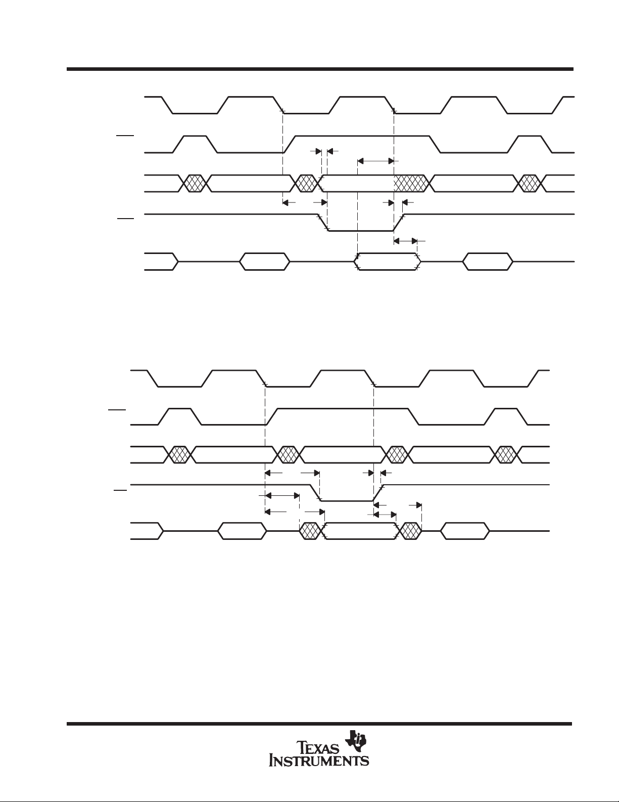
Timing measurements are referenced to and from a low voltage of 0.8 volts and a high voltage of 2 volts, unless
otherwise noted.
clock timing
†
t
d(MCC)
and t
X2/CLKIN
CLKOUT
w(MCP)
t
r(MC)
t
c(MC)
t
w(MCL)
t
f(MC)
d(MCC)
t
f(C)
†
t
w(CL)
t
are referenced to an intermediate level of 1.5 V on the CLKIN waveform.
t
w(MCH)
t
c(C)
t
w(MCP)
t
r(C)
†
t
w(CH)
memory read timing
CLKOUT
t
d3
MEN
A11-A0
D15-D0
t
c(C)
t
d2
t
t
d1
su(A-MD)
Address Bus Valid
t
su(D)
Instruction Valid
t
h(A-WMD)
t
h(D)
POST OFFICE BOX 1443 • HOUSTON, TEXAS 77001
23
TMS320C10, TMS320C10-14, TMS320C10-25
DIGITAL SIGNAL PROCESSORS
SPRS009C–JANUARY 1987– REVISED JULY 1991
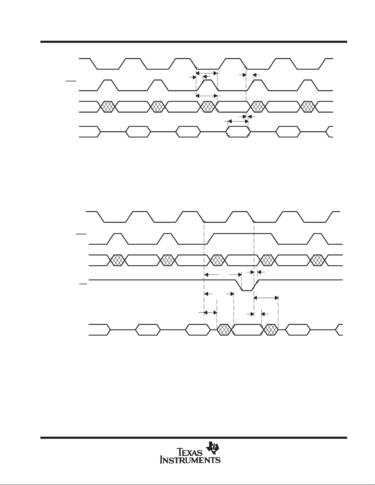
TBLR instruction timing
CLKOUT
t
MEN
A11-A0
D15-D0
Legend:
1. TBLR Instruction Prefetch 7. Address Bus V alid
2. Dummy Prefetch 8. Address Bus Valid
3. Data Fetch 9. Instruction Valid
4. Next Instruction Prefetch 10. Instruction Valid
5. Address Bus Valid 11. Data Input Valid
6. Address Bus Valid 12. Instruction Valid
12 3 4
5678
9101112
d3
t
su(D)
t
d2
t
d1
t
h(D)
t
d3
TBLW instruction timing
CLKOUT
MEN
A11-A0
WE
D15-D0
Legend:
1. TBLW Instruction Prefetch 7. Address Bus Valid
2. Dummy Prefetch 8. Instruction Valid
3. Next Instruction Prefetch 9. Instruction Valid
4. Address Bus Valid 10. Data Output Valid
5. Address Bus Valid 11. Instruction Valid
6. Address Bus Valid
12 3
4567
891011
t
d6
t
d8
t
d9
t
v
t
d7
t
d10
24
POST OFFICE BOX 1443 • HOUSTON, TEXAS 77001
IN instruction timing
CLKOUT
TMS320C10, TMS320C10-14, TMS320C10-25
DIGITAL SIGNAL PROCESSORS
SPRS009C–JANUARY 1987–REVISED JUL Y 1991
MEN
A11-A0
DEN
D15-D0
Legend:
1. IN Instruction Prefetch 5. Address Bus Valid
2. Next Instruction Prefetch 6. Instruction Valid
3. Address Bus Valid 7. Data Input Valid
4. Peripheral Address Valid 8. Instruction Valid
12
345
t
d4
678
OUT instruction timing
CLKOUT
MEN
12
t
su(A-MD)
t
su(D)
t
d5
t
h(D)
A11-A0
WE
D15-D0
Legend:
1. OUT Instruction Prefetch 5. Address Bus Valid
2. Next Instruction Prefetch 6. Instruction Valid
3. Address Bus Valid 7. Data Output Valid
4. Peripheral Address Valid 8. Instruction Valid
34 5
t
d6
t
d9
t
d8
678
t
d7
t
t
v
d10
POST OFFICE BOX 1443 • HOUSTON, TEXAS 77001
25
TMS320C10, TMS320C10-14, TMS320C10-25
DIGITAL SIGNAL PROCESSORS
SPRS009C–JANUARY 1987– REVISED JULY 1991
reset timing
CLKOUT
t
su(R)
RS
t
w(R)
DEN
MEN
D15-D0
MEN
WE
(see
Note E)
t
dis(R)
Data
Out
t
d11
Data Shown Relative to WE
t
su(R)
Data In From
PC ADDR 0
Data In From
PC ADDR PC+1
AB = Address Bus
Address
Bus
NOTES: A. RS forces DEN, WE, and MEN high and places data bus D0 through D15 in a high-impedance state. AB outputs (and program count-
er) are synchronously cleared to zero after the next complete CLK cycle from RS
B. RS
must be maintained for a minimum of five clock cycles.
C. Resumption of normal program will commence after one complete CLK cycle from RS
D. Due to the synchronization action on RS
cycle.
E. Diagram shown is for definition purpose only . DEN
F. During a write cycle, RS
AB = PC AB = PC+1
, time to execute the function can vary dependent upon when RS↑ or RS↓ occur in the CLK
, WE, and MEN are mutually exclusive.
may produce an invalid write address.
AB = PC = 0
↓.
↑.
AB = PC+1
interrupt timing
CLKOUT
t
su(INT)
INT
t
f(INT)
t
w(INT)
BIO timing
26
CLKOUT
BIO
t
su(IO)
t
f(IO)
t
w(IO)
POST OFFICE BOX 1443 • HOUSTON, TEXAS 77001
TMS320C10, TMS320C10-14, TMS320C10-25
DIGITAL SIGNAL PROCESSORS
SPRS009C–JANUARY 1987–REVISED JUL Y 1991
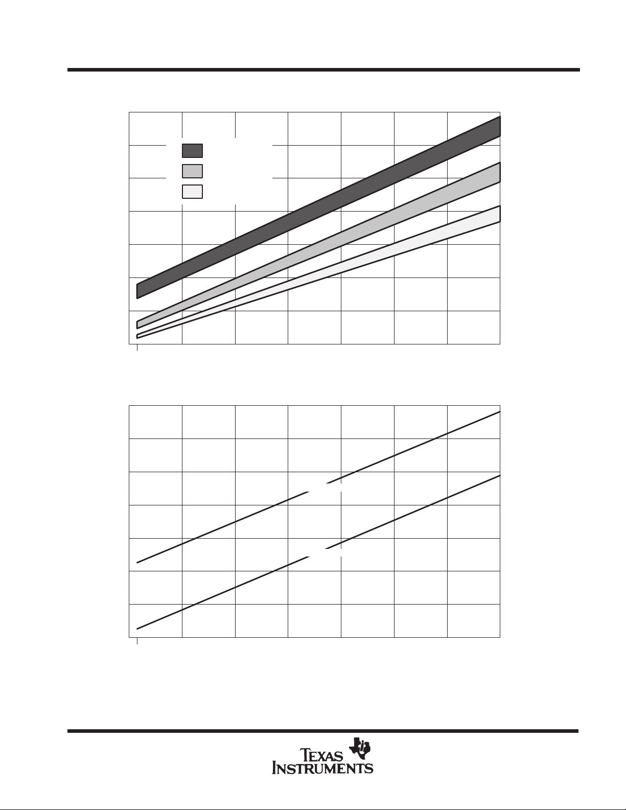
TYPICAL POWER VS. FREQUENCY GRAPHS
52
46
40
34
28
- Supply Current - mAI
CC
I
22
16
10
1.2 4 8 12 16 20 24 28
42
VCC = 5.5 V
VCC = 5.0 V
VCC = 4.5 V
fx - Crystal Frequency - MHz
(a) – 40°C to 85°C Temperature Range
TA = – 40°C
TA = 85°C
TA = – 40°C
TA = 85°C
TA = – 40°C
TA = 85°C
36
30
With Load
24
18
- Supply Current - mA
CC
12
6
0
1.2 4 8 12 16 20 24 28
(b) Voltage = 5 V; Temperature = 25°C
Without Load
fx - Crystal Frequency - MHz
Figure 4. Typical CMOS ICC vs Frequency
POST OFFICE BOX 1443 • HOUSTON, TEXAS 77001
27
TMS320C14, TMS320E14, TMS320P14
DIGITAL SIGNAL PROCESSORS
SPRS009C–JANUARY 1987– REVISED JULY 1991
Key Features: TMS320C14/E14/P14
• 160-ns Instruction Cycle
• 256 Words of On-Chip Data RAM
• 4K Words of On-Chip Program ROM
(TMS320C14)
• 4K Words of On-Chip Program EPROM
(TMS320E14/P14)
• One-Time Programmable (OTP) Windowless
EPROM Version Available (′320P14)
• EPROM Code Protection for Copyright Security
• External Memory Expansion up to 4K-Words
at Full Speed (Microprocessor Mode)
• 16 × 16-Bit Multipler With 32-Bit Product
• 0 to 16-Bit Barrel Shifter
• Seven Input and Seven Output External Ports
• Bit Selectable I/O Port (16 Pins)
• 16-Bit Bidirectional Data Bus With Greater than
50-Mbps Transfer Rate
• Asynchronous Serial Port
• 15 Internal/External Interrupts
• Event Manager With Capture Inputs and
Compare Outputs
• Four Independent Timers [Watchdog,
General Purpose (2), Serial Port]
• Four-Level Hardware Stack
• Packaging: 68-Pin PLCC (FN Suffix)
or CLCC (FZ Suffix)
• Single 5-V Supply
• Operating Free-Air Temperature
...0°C to 70°C
Interrupt
TCLK/CLKR
TCLK2/CLKX
WE
REN
RS
INT
CLKOUT
/MC/MP
NMI
WDT
CLKIN
+5 V GND
256-Word RAM
8K-Word ROM/
EPROM
32-Bit ALU/ACC
Multiplier
Shifters
TMS320C14, TMS320E14/P14
FN/FZ Packages
(Top View)
CC2VSS2
V
CMP3
CAP0
A9
CMP0
CMP1
A10
A11
9876543216867666564636261
10
11
A8
12
A7
13
A6
14
15
16
17
18
19
A5
20
A4
21
22
23
24
A3
25
A2
26
27 28 2930 31 32 33 34 35 3637 38 39 40 41 42 43
A1
A0
IOP15
IOP14
IOP13
V
IOP12
CC1
CMP2
D15
SS1
V
D14
CAP1
IOP11
Address (12)
D2
CMP5/CAP3/FSX
AMP4/CAP2/FSR
D0
D1
D13
D12
IOP9
IOP10
IOP8
Data (16)
D3
D4
60
D5
59
D6
58
D7
57
IOP0
56
IOP1
55
IOP2
54
IOP3
53
IOP4
52
IOP5
51
D8
50
D9
49
RXD/DATA
48
TXD/CLK
47
D10
46
IOP6
45
IOP7
44
D11
28
POST OFFICE BOX 1443 • HOUSTON, TEXAS 77001

TMS320C14, TMS320E14, TMS320P14
DIGITAL SIGNAL PROCESSORS
SPRS009C–JANUARY 1987–REVISED JUL Y 1991
introduction
The ′C14/E14/P14 are 16/32-bit single-chip digital signal processing (DSP) microcontrollers that combine the
high performance of a DSP with on-chip peripherals. With a 160-ns instruction cycle, these devices are capable
of executing up to 6.4 million instructions per second (MIPS). The ′C14/E14/P14 DSPs are ideal for applications
such as automotive control systems, computer peripherals, industrial controls, and military command/control
system applications.
Control-specific on-chip peripherals include: An event manager with 6 channel PWM D/A/, 6-bit I/O pins, an
asynchronous serial port, four 16-bit timers, and internal/external interrupts.
With 4K-words of on-chip ROM, the ′C14 is a mask programmable device. Code is provided by the customer,
and TI incorporates the customer’s code into the photomask. It is offered in a 68-pin plastic chip carrier package
(FN suffix), rated for operation from 0°C to 70°C.
The ′E14 is provided with a 4K-word on-chip EPROM. This EPROM version is excellent for prototyping and for
customized applications. It is programmable with standard EPROM programmers. It is offered in a 68-pin
(windowed) cerquad package (FZ suffix), rated for operation from 0°C to 70°C.
The ′P14 features a one-time programmable 4K-word on-chip EPROM. The ′P14 is provided in an
unprogrammed state and is programmed as if it were a blank ′E14. It is offered in a low-cost,
volume-production-oriented, 68-pin plastic leaded chip carrier (PLCC) package (FN suffix), rated for operation
from 0°C to 70°C.
POST OFFICE BOX 1443 • HOUSTON, TEXAS 77001
29
TMS320C14, TMS320E14, TMS320P14
DIGITAL SIGNAL PROCESSORS
SPRS009C–JANUARY 1987– REVISED JULY 1991
Each device can execute programs form either internal (MC/MP=0) or external program memory (MC/MP=1).
For proprietary code security, the ′E14 and ′P14 incorporate an EPROM protect bit (RBIT). If this bit is
programmed, the device’s internal program memory cannot be accessed by any external means.
TERMINAL FUNCTIONS
PIN DESCRIPTION
NAME NO.
A11
A10
A9
A8
A7
A6
A5
A4
A3
A2/PA2
A1/PA1
A0/PA0
D15 MSB
D14
D13
D12
D11
D10
D9
D8
D7
D6
D5
D4
D3
D2
D1
D0 LSB
INT 18 I External interrupt input. The interrupt signal is generated by a high-to-low transition on this pin.
NMI/MC/MP 22 I Non-maskable interrupt. When this pin is brought low, the device is interrupted irrespective of the
5
6
9
12
13
14
20
21
25
26
27
28
35
36
39
40
43
46
49
50
57
58
59
60
61
62
63
64
†
I/O/Z
O/Z Program memory address bus A11 (MSB) through A0 (LSB) and port addresses P A2 (MSB) through
I/O/Z Parallel data bus D15 (MSB) through D0 (LSB). The data bus is always in the high-impedance state
PA0 (LSB). Addresses A11 through A0 are always active and never go to high impedance except
during reset. During execution of the IN and OUT instructions, pins 26, 27, and 28 carry the port
addresses. Pins A3 through A11 are held high when port accesses are made on pins PA0 through
PA2.
except when WE
state of the INTM bit in status register ST.
is active (low). The data bus is also active when internal peripherals are written to.
INTERRUPT AND MISCELLANEOUS SIGNALS
ADDRESS/DATA BUSES
Microcomputer/microprocessor select. This pin is also sampled when RS
internal program memory is selected. If low during reset, external memory will be selected.
WE 15 O Write enable. When active low, WE indicates that device will output data on the bus.
REN 16 O Read enable. When active low, REN indicates that device will accept data from the bus.
RS 17 I Reset. When this pin is low, the device is reset and PC is set to zero.
Continued next page.
†
Input/Output/High-impedance state.
30
POST OFFICE BOX 1443 • HOUSTON, TEXAS 77001
is low. If high during reset,

DIGITAL SIGNAL PROCESSORS
SPRS009C–JANUARY 1987–REVISED JUL Y 1991
TERMINAL FUNCTIONS (concluded)
TMS320C10-14
PIN DESCRIPTION
NAME NO.
CLKOUT 19 O System clock output (one fourth CLKIN frequency).
V
CC
V
SS
CLKIN 24 I Master clock input from external clock source.
RXD 48 I Asynchronous mode receive input.
TXD 47 O/Z Asynchronous mode transmit output.
TCLK1 10 I Timer 1 clock. If external clock is selected, it serves as clock input to Timer 1.
TCLK2 11 I Timer 2 clock. If external clock is selected, it serves as clock input to Timer 2.
WDT 23 O W atchdog timer output. An active low is generated on this pin when the watchdog timer times out.
IOP15 MSB
IOP14
IOP13
IOP12
IOP11
IOP10
IOP9
IOP8
IOP7
IOP6
IOP5
IOP4
IOP3
IOP2
IOP1
IOP0 LSB
CMP0
CMP1
CMP2
CMP3
CAP0
CAP1
CMP4/CAP2 66 I/O This pin can be configured as compare output or capture input.
CMP5/CAP3 65 I/O This pin can be configured as compare output or capture input.
†
Input/Output/High-impedance state.
4,33 I 5-V supply pins.
3,34 I Ground pins.
29
30
31
32
37
38
41
42
44
45
51
52
53
54
55
56
8
7
2
1
68
67
†
I/O/Z
I/O 16 bit I/O lines that can be individually configured as inputs or outputs and also individually set or
reset
when configured as outputs.
O Compare outputs. The states of these pins are determined by the combination of compare and action
registers.
I Capture inputs. A transition on these pins causes the timer register to be captured in FIFO stack.
SUPPLY/OSCILLATOR SIGNALS
SERIAL PORT AND TIMER SIGNALS
BIT I/O PINS
COMPARE AND CAPTURE SIGNALS
POST OFFICE BOX 1443 • HOUSTON, TEXAS 77001
31

TMS320C14, TMS320E14, TMS320P14
DIGITAL SIGNAL PROCESSORS
SPRS009C–JANUARY 1987– REVISED JULY 1991
functional block diagram
CLKOUTCLKIN
NMI/
MC/MP
INT
WE
REN
RS
Interrupt
Controller
Controller
A0-A11
PA0-PA2
16
ARP
BSR
16
MUX
12
12 LSB
MUX
12
12
PC (12)
12
12
Stack
4
3
× 12
Program Bus
16
AR0 (16)
AR1 (16)
Data Bus
16 16
7
8
8
MUX
8
Address
Data
(256 Words)
Data
16 16
Data Bus
16
Instruction
Program
ROM/EPROM
(4K Words)
Address
16
16
1
DP
Shifter
(0–16)
32
32
Shifter (0,1,4)
T(16)
Multiplier
P(32)
32
ALU (32)
32
ACC (32)
32
32
MUX
Watchdog Timer
Timers
16
16
MUX
16
16
32
16
1.2
16
16
16
16
16
9
9
IOP
Legend: DP = Data Page Pointer
ACC= Accumulator IOP = Input/Output Port
ACT = Action Register (Bit Selectable)
ALU = Arithmetic Logic Unit PC = Program Counter
ARP = Auxiliary Register Point P = P Register
AR0 = Auxiliary Register 0 RBR = Receive Buffer Register
AR1 = Auxiliary Register 1 RSR = Receive Shift Register
BSR = Bank Select Register T = T Register
CAP = Capture TBR = Transmit Buffer Register
CMPR = Compare Register TSR = Transmit Shift Register
CMPR
(6)
4
× 16
FIFO
Stack
(4)
Serial
Port
Timer
16
16
6
ACT
(6)
CAP
4
Detect
(4)
Serial
Port
Controller
TBR
TSR
RBR
RSR
WDT
TCLK1.2
D15-D0
CMP0-CMP3
CMP4, 5 /
CAP2, 3
CAP0,1
TXD
RXD
IOP0-IOP15
architecture
The ′C1x family utilizes a modified Harvard architecture for speed and flexibility . In a strict Harvard architecture,
program and data memory lie in two separate spaces, permitting a full overlap of instruction fetch and execution.
The ′C1x family’s modification of a Harvard architecture allows transfers between program and data spaces,
thereby increasing the flexibility of the device. This modification permits coefficients stored in program memory
to be read into the RAM, eliminating the need for a separate coefficient ROM. It also makes available immediate
instructions and subroutines based on computed values.
32-bit ALU/accumulator
The ′C14/E14/P14 devices contain a 32-bit ALU and accumulator for support of double-precision,
twos-complement arithmetic. The ALU is a general-purpose arithmetic unit that operates on 16-bit words taken
from the data RAM or derived from immediate instructions. In addition to the usual arithmetic instructions, the
ALU can perform Boolean operations, providing the bit manipulation ability required of a high-speed controller.
32
POST OFFICE BOX 1443 • HOUSTON, TEXAS 77001

TMS320C14, TMS320E14, TMS320P14
DIGITAL SIGNAL PROCESSORS
SPRS009C–JANUARY 1987–REVISED JUL Y 1991
The accumulator stores the output from the ALU and is often an input to the ALU. It operates with a 32-bit
wordlength. The accumulator is divided into a high-order word (bits 31 through 16) and a low-order word (bits
15 through 0). Instructions are provided for storing the high- and low- order accumulator words in memory.
shifters
Two shifters are available for manipulating data. The ALU barrel shifter performs a left-shift of 0 to16 places on
data memory words loaded into the ALU. This shifter extends the high-order bit of the data word and zero-fills
the low-order bits for twos-complement arithmetic. The accumulator parallel shifter performs a left-shift of 0, 1,
or 4 places on the entire accumulator and places the resulting high-order accumulator bits into data RAM. Both
shifters are useful for scaling and bit extraction
16 × 16-bit parallel multiplier
The multiplier performs a 16 × 16-bit twos-complement multiplication with a 32-bit result in a single instruction
cycle. The multiplier consists of three units: the T Register, P Register, and the multiplier array. The 16-bit T
Register temporarily stores the multiplicand; the P Register stores the 32-bit product. Multiplier values either
come from the data memory or are derived immediately from the MPYK (multiply immediate) instruction word.
The fast on-chip multiplier allows the device to perform fundamental operations such as convolution, correlation,
and filtering.
data and program memory
Since the ′C14/E14/P14 devices use a Harvard architecture, data and program memory reside in two separate
spaces. These devices have 256 words of on-chip data RAM and 4K words of on-chip program ROM (′C14)
or EPROM (′E14 and the OTP ′P14). The EPROM cell utilizes standard PROM programmers and is
programmed identically to a 64K-bit CMOS EPROM (TMS27C64).
program memory expansion
The ′C1x devices are capable of executing up to 4K words of external memory at full speed for those applications
requiring external program memory space. This allows for external RAM-based systems to provide multiple
functionality.
microcomputer/microprocessor operating modes
The ′C14/E14/P14 devices offer two modes of operation defined by the state of the NMI
the microcomputer mode (NMI/MC/MP is high) or the microprocessor mode (NMI/MC/MP is low). In the
microcomputer mode, the on-chip ROM is mapped into the program memory space. In the microprocessor
mode, all 4K words of memory are external.
interrupts and subroutines
The ′C14/E14/P14 devices contain a four-level hardware stack for saving the contents of the program counter
during interrupts and subroutine calls. Instructions are available for saving the complete context of the device.
PUSH and POP instructions permit a level of nesting restricted only by the amount of available RAM. The
′C14/E14/P14 have a total of 15 internal/external interrupts. Fourteen of these are maskable; NMI
fifteenth.
input/output
The 16-bit parallel data bus can be utilized to access external peripherals. However, only the lower three address
lines are active. The upper nine address lines are driven high.
bit I/O
The ′C14/E14/P14 has 16 pins of bit I/O that can be individually configured as inputs or outputs. Each of the
pins can be set or cleared without affecting the others. The input pins can also detect and match patterns and
generate a maskable interrupt signal to the CPU.
/MC/MP pin during reset:
is the
serial port
The ′C14/E14/P14 includes an I/O-mapped asynchronous serial port.
POST OFFICE BOX 1443 • HOUSTON, TEXAS 77001
33

TMS320C14, TMS320E14, TMS320P14
DIGITAL SIGNAL PROCESSORS
SPRS009C–JANUARY 1987– REVISED JULY 1991
event manager
An event manager is included that provides up to four capture inputs and up to six compare outputs. This
peripheral operates with the timers to provide a form of programmable event logging/detection. The six compare
outputs can also be configured to produce six channels of high precision PWM.
timers 1 and 2
Two identical 16-bit timers are provided for general purpose applications. Both timers include a 16-bit period
register and buffer latch, and can generate a maskable interrupt.
serial port timer
The serial port timer is a 16-bit timer primarily intended for baud rate generation for the serial port. Its architecture
is the same as timers 1 and 2, therefore it can serve as a general purpose timer if not needed for serial
communication.
watchdog timer
The ′C14/E14/P14 contain a 16-bit watchdog timer that can produce a timeout (WDT
applications such as software development and event monitoring. The watchdog timer also generates, at the
point of the timeout, a maskable interrupt signal to the CPU.
instruction set
) signal for various
A comprehensive instruction set supports both numeric-intensive operations, such as signal processing, and
general-purpose operations, such as high-speed control. All of the first-generation devices are object-code
compatible and use the same 60 instructions. The instruction set consists primarily of single-cycle single-word
instructions, permitting execution rates of more than six million instructions per second. Only infrequently used
branch and I/O instructions are multicycle. Instructions that shift data as part of an arithmetic operation execute
in a single cycle and are useful for scaling data in parallel with other operations.
NOTE
The BIO pin on other ′C1x devices is not available for use in the ′C14/E14/P14 devices. An attempt to
execute the BIOZ (Branch on BIO
Three main addressing modes are available with the instruction set: direct, indirect, and immediate addressing.
direct addressing
In direct addressing, seven bits of the instruction word concatenated with the 1-bit data page pointer from the
data memory address. This implements a paging scheme in which each page contains 128 words.
indirect addressing
Indirect addressing forms the data memory address from the least-significant eight bits of one of the two
auxiliary registers, AR0 and AR1. The Auxiliary Register Pointer (ARP) selects the current auxiliary register. The
auxiliary registers can be automatically incremented or decremented and the ARP changed in parallel with the
execution of any indirect instruction to permit single-cycle manipulation of data tables. Indirect addressing can
be used with all instructions requiring data operands, except for the immediate operand instructions.
immediate addressing
Immediate instructions derive data from part of the instruction word rather than from part of the data RAM. Some
useful immediate instructions are multiply immediate (MPYK), load accumulator immediate (LACK), and load
auxiliary register immediate (LARK).
low) instruction will result in a two cycle NOP action.
34
POST OFFICE BOX 1443 • HOUSTON, TEXAS 77001

TMS320C14, TMS320E14, TMS320P14
DIGITAL SIGNAL PROCESSORS
SPRS009C–JANUARY 1987–REVISED JUL Y 1991
electrical specifications
This section contains all the electrical specifications for the ′C14/E14/P14 devices, including test parameter
measurement information. Parameters with PP subscripts apply only to the ′E14 and ′P14 in the EPROM
programming mode.
absolute maximum ratings over specified temperature range (unless otherwise noted)
Supply voltage range, VCC (see Note 6) –0.3 V to 7 V. . . . . . . . . . . . . . . . . . . . . . . . . . . . . . . . . . . . . . . . . . . . . .
Supply voltage range, VPP (see Note 6) –0.6 V to 14 V. . . . . . . . . . . . . . . . . . . . . . . . . . . . . . . . . . . . . . . . . . . . .
Input voltage range –0.3 V to 14 V. . . . . . . . . . . . . . . . . . . . . . . . . . . . . . . . . . . . . . . . . . . . . . . . . . . . . . . . . . . . . . .
Output voltage range –0.3 V to 7 V. . . . . . . . . . . . . . . . . . . . . . . . . . . . . . . . . . . . . . . . . . . . . . . . . . . . . . . . . . . . . . .
Continuous power dissipation 0.5 W. . . . . . . . . . . . . . . . . . . . . . . . . . . . . . . . . . . . . . . . . . . . . . . . . . . . . . . . . . . . .
Air temperature range above operating device: L version 0
Storage temperature –55 °C + 150 °C. . . . . . . . . . . . . . . . . . . . . . . . . . . . . . . . . . . . . . . . . . . . . . . . . . . . . . . . . . . .
†
Stresses beyond those listed under “Absolute Maximum Ratings” may cause permanent damage to the device. This is a stress rating only, and
functional operation of the device at these or any other conditions beyond those indicated in the “Recommended Operating Conditions” section of
this specification is not implied. Exposure to absolute-maximum-rated conditions for extended periods may affect device reliability .
NOTE 6: All voltage values are with respect to VSS.
recommended operating conditions
MIN NOM MAX UNIT
Operating voltage 4.75 5 5.25 V
Fast programming 5.75 6 6.25 V
V
Supply voltage
CC
SNAP! Pulse programming 6.25 6.5 6.75 V
V
Supply voltage for Fast programming (see Note 11) 12.25 12.5 12.75 V
PP
V
Supply voltage for SNAP! Pulse programming (see Note 11) 12.75 13 13.25 V
PP
V
Supply voltage 0 V
SS
V
High-level input voltage V
IH
V
Low-level input voltage, all inputs 0.8 V
IL
I
High-level output current, all outputs –300 µA
OH
I
Low-level output current, all outputs 2 mA
OL
T
Operating free-air temperature 0 70
A
NOTE 11: VPP can be applied only to programming pins designed to accept VPP as an input. During programming the total supply current
is IPP + ICC.
CLKIN, CAP0, CAP1, CMP4/CAP2, CMP5/CAP3, RS 3
All remaining inputs 2
†
°
C to 70 °C. . . . . . . . . . . . . . . . . . . . . . . . . . . . . . . .
°
C
POST OFFICE BOX 1443 • HOUSTON, TEXAS 77001
35

TMS320C14, TMS320E14, TMS320P14
DIGITAL SIGNAL PROCESSORS
SPRS009C–JANUARY 1987– REVISED JULY 1991
electrical characteristics over specified temperature range (unless otherwise noted)
PARAMETER TEST CONDITIONS MIN TYP
V
High-level output voltage
OH
V
Low-level output voltage IOL = MAX 0.3 0.5 V
OL
I
Off-state output voltage
OZ
I
Input current
I
§
I
Supply current f = 25.6 MHz, VCC = 5.25 V, TA = 0°C to 70°C 70 90 mA
CC
I
PP1VPP
I
PP2
C
I
C
O
†
All typical values are at VCC = 5 V, TA = 25°C, except ICC at 70°C.
‡
Values derived from characterization data and not tested.
§
ICC characteristics are inversely proportional to temperature.
NOTE 7: This voltage specification is included for interface to HC logic. However, note that all of the other timing parameters defined in this data
supply current VPP = VCC = 5.5 V 100 µA
VPP supply current
(during program pulse)
Input capacitance pF
Output
capacitance
sheet are specified for TTL logic levels and will differ for HC logic levels.
Data bus 25
All others 15
Data bus 25
All others 10
IOH = MAX 2.4 3 V
IOH = 20 µA (see Note 7) VCC – 0.4
VCC = MAX µA
VI = VSS to V
VPP = 13 V 30 50 mA
f = 1 MHz, All other pins 0 V
VO = 2.4 V 20
VO = 0.4 V –20
All other inputs except CLKIN ±20
CC
CLKIN ±50
†
†
‡
‡
‡
‡
MAX UNIT
V
µA
pF
PARAMETER MEASUREMENT INFORMATION
2.15 V
RL = 825 Ω
From Output
Under Test
Test
Point
CL = 100 pF
Figure 5. Test Load Circuit
EXTERNAL CLOCK REQUIREMENTS
The TMS320C14/E14/P14 use an external frequency source for a clock. This source is applied to the CLKIN
pin, and must conform to the specifications in the table below.
PARAMETERS TEST CONDITIONS MIN NOM MAX UNIT
CLKIN Input clock frequency TA = 0°C to 70°C 6.7 25.6 MHz
36
POST OFFICE BOX 1443 • HOUSTON, TEXAS 77001

TMS320C14, TMS320E14, TMS320P14
DIGITAL SIGNAL PROCESSORS
SPRS009C–JANUARY 1987–REVISED JUL Y 1991
CLOCK TIMING
switching characteristics over recommended operating conditions
PARAMETER TEST CONDITIONS MIN NOM MAX UNIT
t
c(C)
t
r(C)
t
f(C)
t
w(CL)
t
w(CH)
t
d(MCC)
†
Values were derived from characterization data and not tested.
CLKOUT cycle time
CLKOUT rise time
CLKOUT fall time 8
Pulse duration, CLKOUT low 72
Pulse duration, CLKOUT high 70
Delay time CLKIN↑ to CLKOUT↓ 45
timing requirements over recommended operating conditions
t
c(MC)
t
r(MC)
t
f(MC)
t
w(MCP)
t
w(MCL)
t
w(MCH)
†
Values were derived from characterization data and not tested.
‡
t
c(C)
Master clock cycle time
Rise time, master clock input 5
Fall time, master clock input 5
Pulse duration, master clock 0.45 t
Pulse duration, master clock low 15
Pulse duration, master clock high 15
is the cycle time of CLKOUT, i.e., 4t
‡
RL = 825 Ω,
CL = 100 pF,
(see Figure 2)
‡
(4 times CLKIN cycle time if an external oscillator is used).
c(MC)
156.25 600 ns
MIN NOM MAX UNIT
39.06 40 150 ns
c(MC)
†
10
†
†
†
†
†
†
†
†
†
†
10
†
10
0.55 t
c(MC)
130 ns
130 ns
ns
ns
ns
ns
ns
ns
ns
†
ns
POST OFFICE BOX 1443 • HOUSTON, TEXAS 77001
37

TMS320C14, TMS320E14, TMS320P14
DIGITAL SIGNAL PROCESSORS
SPRS009C–JANUARY 1987– REVISED JULY 1991
MEMORY READ AND INSTRUCTION TIMING
switching characteristics over recommended operating conditions
PARAMETER
t
su(A)R
t
su(A)W
t
h(A)
t
en(D)W
t
su(D)W
t
h(D)W
t
dis(D)W
t
w(WEL)
t
w(RENL)
t
rec(WE)
t
rec(REN)
t
d(WE-CLK)
†
Values were derived from characterization data and not tested.
Address bus valid before REN↓ 0.25 t
Address bus valid before WE↓
Address bus valid after REN↑ or WE↑ 5
Data starts being driven before WE↓ 0.25 t
Data valid prior to WE↓ 0.25 t
Data valid after WE↑ 0.25 t
Data in high impedance after WE↑ 0.25 t
WE-low duration 0.50 t
REN-low duration 0.75 t
Write recovery time, time between WE↑ and REN↓ 0.25 t
Read recovery time, time between REN↑ and WE↓ 0.50 t
Time from WE↑ to CLKOUT↑ 0.50 t
TEST
CONDITIONS
RL = 825 Ω,
CL = 100 pF,
(see Figure 2)
MIN NOM MAX UNIT
c(C)
0.50 t
c(C)
c(C)
c(C)
c(C)
c(C)
c(C)
c(C)
–39 ns
–45 ns
†
c(C)
–45 ns
–10 ns
+ 25
c(C)
–15 ns
–15 ns
–5 ns
c(C)
–10 ns
–15 ns
ns
†
ns
†
ns
timing requirements over recommended operating conditions
TEST CONDITIONS MIN NOM MAX UNIT
t
su(D)R
t
h(D)R
t
a(A)
t
oe(REN)
t
dis(D)R
Data set-up prior to REN↑ 52 ns
Data hold after REN↑
Access time for read cycle data
valid after valid address
Access time for read cycle from REN↓ 0.75 t
Data in high impedance after REN↑ 0.25 t
RL = 825 Ω,
CL = 100 pF,
(see Figure 2)
0 ns
RESET (RS) TIMING
switching characteristics over recommended operating conditions
PARAMETER TEST CONDITIONS MIN NOM MAX UNIT
t
d(RS-RW)
t
dis(RS-RW)
t
dis(RS-DB)
t
dis(RS-AB)
t
en(RS-AB)
Delay from RS↓ to REN↑ and WE↑ 0.75 t
Delay from RS↓ to REN and
WE
into high impedance
Data bus disable after RS↓ 1.25 t
Address bus disable after RS↓ t
Address bus enable after RS↑ t
RL = 825 Ω,
CL = 100 pF,
(see Figure 2)
timing requirements over recommended operating conditions
TEST CONDITIONS MIN NOM MAX UNIT
t
su(RS)
t
w(RS)
NOTE 10: RS can occur anytime during the clock cycle. Time given is minimum to ensure synchronous operation.
RS setup prior to CLKOUT↓ (see Note 10) 60 ns
RS pulse duration
RL = 825 Ω,
CL = 100 pF,
(see Figure 2)
5t
c(C)
t
c(C)
c(C)
c(C)
1.25 t
–90 ns
–60 ns
†
c(C)
†
+ 20
†
c(C)
†
c(C)
†
c(C)
†
c(C)
ns
ns
ns
ns
ns
ns
ns
38
POST OFFICE BOX 1443 • HOUSTON, TEXAS 77001

TMS320C14, TMS320E14, TMS320P14
DIGITAL SIGNAL PROCESSORS
SPRS009C–JANUARY 1987–REVISED JUL Y 1991
MICROCOMPUTER/MICROPROCESSOR MODE (NMI/MC/MP)
timing requirements over recommended operating conditions
MIN NOM MAX UNIT
t
h(MC/MP)
†
Values were derived from characterization data and not tested.
‡
Hold time to put device in microprocessor mode.
timing requirements over recommended operating conditions
t
f(INT)
t
f(NMI)
t
w(INT)
t
w(NMI)
t
su(INT)
t
su(NMI)
NOTE 12: INT and NMI are synchronous inputs and can occur at any time during the cycle. NMI and INT are edge triggered only.
‡
Hold time after RS high t
c(C)
INTERRUPT (INT)/NONMASKABLE INTERRUPT (NMI)
MIN NOM MAX UNIT
Fall time, INT 15
Fall time, NMI 15
Pulse duration, INT t
Pulse duration, NMI t
Setup time, INT before CLKOUT low (see Note 12) 60 ns
Setup time, NMI before CLKOUT low (see Note 12) 60 ns
c(C)
c(C)
ns
†
ns
†
ns
ns
ns
BIT I/O TIMING
switching characteristics over recommended operating conditions
PARAMETER TEST CONDITIONS MIN NOM MAX UNIT
t
rfo(IOP)
t
d(IOP)
Rise and fall time outputs 20
CLKOUT low to data valid outputs
RL = 825 Ω,
CL = 100 pF,
(see Figure 2)
timing requirements over recommended operating conditions
TEST CONDITIONS MIN NOM MAX UNIT
t
rfl(IOP)
t
su(IOP)
t
w(IOP)
Rise and fall time inputs 20
Data setup time before CLKOUT time
Input pulse duration t
RL = 825 Ω,
CL = 100 pF,
(see Figure 2)
GENERAL PURPOSE TIMERS
timing requirements over recommended operating conditions
TEST CONDITIONS MIN NOM MAX UNIT
t
r(TIM)
t
f(TIM)
t
wl(TIM)
t
wh(TIM)
t
clk(TIM)
†
Values were derived from characterization data and not tested.
TCLK1, TCLK2 rise time 20
TCLK1, TCLK2 fall time
TCLK1, TCLK2 low time t
TCLK1, TCLK2 high time t
Input pulse duration 2 t
RL = 825 Ω,
CL = 100 pF,
(see Figure 2)
†
0.75 t
40 ns
c(C)
+20 ns
c(C)
+20 ns
c(C)
+40 ns
c(C)
+80 ns
c(C)
20
†
†
ns
†
ns
ns
ns
ns
POST OFFICE BOX 1443 • HOUSTON, TEXAS 77001
39

TMS320C14, TMS320E14, TMS320P14
DIGITAL SIGNAL PROCESSORS
SPRS009C–JANUARY 1987– REVISED JULY 1991
WATCHDOG TIMER TIMING
switching characteristics over recommended operating conditions
PARAMETER TEST CONDITIONS MIN NOM MAX UNIT
t
f(WDT)
t
d(WDT)
t
w(WDT)
switching characteristics over recommended operating conditions
t
f(CMP)
t
r(CMP)
timing requirements over recommended operating conditions
t
w(CAP)
t
su(CAP)
†
Values were derived from characterization data and not tested.
Fall time, WDT 20
CLKOUT to WDT valid
WDT output pulse duration 7 t
RL = 825 Ω,
CL = 100 pF,
(see Figure 2)
0.25 t
c(C
c(C
EVENT MANAGER TIMER
PARAMETER TEST CONDITIONS MIN NOM MAX UNIT
Fall time, CMP0-CMP5 20
Rise time, CMP0-CMP5
CAP0-CAP3 input pulse duration t
Capture input setup time before CLKOUT low
RL = 825 Ω,
CL = 100 pF,
(see Figure 2)
TEST CONDITIONS MIN NOM MAX UNIT
RL = 825 Ω,
CL = 100 pF,
(see Figure 2)
†
)+20 ns
) ns
20
+20 ns
c(C)
†
20
ns
†
ns
†
ns
ns
40
POST OFFICE BOX 1443 • HOUSTON, TEXAS 77001

TMS320C14, TMS320E14, TMS320P14
DIGITAL SIGNAL PROCESSORS
SPRS009C–JANUARY 1987–REVISED JUL Y 1991
TIMING DIAGRAMS
Timing measurements are referenced to and from a low voltage of 0.8 volts and a high voltage of 2 volts, unless
otherwise noted.
clock timing
X2/CLKIN
CLKOUT
†
t
d(MCC)
and t
are referenced to an intermediate level of 1.5 V on the CLKIN waveform.
w(MCP)
memory read timing
REN
t
r(MC)
t
c(MC)
t
d(MCC)
t
f(C)
t
su(A)R
t
f(MC)
†
t
w(MCL)
t
w(CL)
t
w(MCH)
t
oe(REN)
t
c(C)
t
w(RENL)
t
w(MCP)
t
r(C)
†
t
w(CH)
t
h(A)
A11-A0
D15-D0
Address Bus Valid
t
a(A)
t
su(D)R
Instruction Input Valid
t
h(D)R
POST OFFICE BOX 1443 • HOUSTON, TEXAS 77001
41

TMS320C14, TMS320E14, TMS320P14
DIGITAL SIGNAL PROCESSORS
SPRS009C–JANUARY 1987– REVISED JULY 1991
TBLR instruction timing
REN
A11-A0
D15-D0
Legend:
1. TBLR Instruction Prefetch 7. Address Bus Valid
2. Dummy Prefetch 8. Address Bus Valid
3. Data Fetch 9. Instruction Input Valid
4. Next Instruction Prefetch 10. Instruction Input Valid
5. Address Bus Valid 11. Data Input Valid
6. Address Bus Valid 12. Instruction Input Valid
12 3 4
5678
910 1112
TBLW instruction timing
REN
12 3
t
su(A)R
t
a(A)
t
su(D)R
t
h(D)R
A11-A0
WE
D15-D0
†
Data valid prior to WE
Legend:
1. TBLW Instruction Prefetch 7. Address Bus V alid
2. Dummy Prefetch 8. Instruction Input Valid
3. Next Instruction Prefetch 9. Instruction Input Valid
4. Address Bus Valid 10. Data Output Valid
5. Address Bus Valid 11. Instruction Input Valid
6. Address Bus Valid
↓
4567
891011
t
en(D)W
†
t
su(D)W
t
w(WEL)
†
t
h(D)W
t
dis(D)W
42
POST OFFICE BOX 1443 • HOUSTON, TEXAS 77001

IN instruction timing
TMS320C14, TMS320E14, TMS320P14
DIGITAL SIGNAL PROCESSORS
SPRS009C–JANUARY 1987–REVISED JUL Y 1991
REN
A11-A0
D15-D0
Legend:
1. IN Instruction Prefetch 6. Address Bus Valid
2. Data Fetch 7. Instruction Input Valid
3. Next Instruction Prefetch 8. Data Input Valid
4. Address Bus Valid 9. Instruction Input Valid
5. Peripheral Address Valid
12
t
su(A)R
456
t
a(A)
789
OUT instruction timing
REN
A11-A0
1
3
3
t
su(D)R
t
h(D)R
2
45
WE
D15-D0
Legend:
1. OUT Instruction Prefetch 5. Address Bus Valid
2. Next Instruction Prefetch 6. Instruction Input Valid
3. Address Bus Valid 7. Data Output Valid
4. Peripheral Address Valid
67
t
su(D)W
t
en(D)W
t
w(WEL)
t
h(D)W
t
dis(D)W
POST OFFICE BOX 1443 • HOUSTON, TEXAS 77001
43

TMS320C14, TMS320E14, TMS320P14
DIGITAL SIGNAL PROCESSORS
SPRS009C–JANUARY 1987– REVISED JULY 1991
reset timing
CLKOUT
t
su(RS)
t
dis(RS-RW)
RS
t
w(RS)
REN
(see
WE
Note E)
t
dis(RS-DB)
D15-D0
t
dis(RS-AB)
ADDRESS
BUS
NOTES: A. RS forces REN, and WE high and then places data bus D0-D15, REN, WE, and address bus A0-A1 1 in a high-impedance state.
AB outputs (and program counter) are synchronously cleared to zero after the next complete CLK cycle from RS
B. RS
must be maintained for a minimum of five clock cycles.
C. Resumption of normal program will commence after one complete CLK cycle from RS
D. Due to the synchronization action on RS
cycle.
E. Diagram shown is for definition purpose only. WE
Data Out
AB = PC AB = PC = 0
t
d(RS-RW)
Data Shown Relative To WE
AB = Address Bus
, time to execute the function can vary dependent upon when RS↑ or RS↓ occur in the CLK
and REN are mutually exclusive.
t
su(RS)
t
en(RS-AB)
Data In From
PC ADDR 0
↑.
Data In From
PC ADDR PC+1
AB = PC+1
↑.
microcomputer/microprocessor mode timing
CLKOUT
RS
NMI/MC/MP
t
h(MC/MP)
44
POST OFFICE BOX 1443 • HOUSTON, TEXAS 77001

interrupt timing
CLKOUT
TMS320C14, TMS320E14, TMS320P14
DIGITAL SIGNAL PROCESSORS
SPRS009C–JANUARY 1987–REVISED JUL Y 1991
NMI or INT
bit I/O timing
CLKOUT
IOP15-IOP0
(Output)
IOP15-IOP0
(Input)
t
su(IOP)
t
rfI(IOP)
t
f(INT)
t
w(INT)
t
su(INT)
, t
f(NMI)
, t
w(NMI)
, t
su(NMI)
t
w(IOP)
t
rfo(IOP)
general purpose timers
TCLK1, TCLK2
t
r(TIM)
watchdog timer
CLKOUT
WDT
t
d(WDT)
t
wh(TIM)
t
clk(TIM)
t
f(WDT)
t
f(TIM)
t
wl(TIM)
t
w(WDT)
POST OFFICE BOX 1443 • HOUSTON, TEXAS 77001
45

TMS320C14, TMS320E14, TMS320P14
DIGITAL SIGNAL PROCESSORS
SPRS009C–JANUARY 1987– REVISED JULY 1991
event manager
CLKOUT
CAP3-CAP0
CMP5-CMP0
t
su(CAP)
t
w(CAP)
t
f(CMP)
/ t
r(CMP)
46
POST OFFICE BOX 1443 • HOUSTON, TEXAS 77001

TMS320E14, TMS320P14
DIGITAL SIGNAL PROCESSORS
SPRS009C–JANUARY 1987–REVISED JUL Y 1991
PROGRAMMING THE TMS320E14/P14 EPROM CELL
The ′E14 and ′P14 include a 4K × 16-bit industry-standard EPROM cell for prototyping and low-volume
production. The ′C14 with a 4K-word masked ROM then provides a migration path for cost-effective production.
An EPROM adapter socket (part # TMDX32701 10), shown in Figure 5, is available to provide 68-pin to 28-pin
conversion for programming the ′E14 and ′P14.
Key features of the EPROM cell include the normal programming operation as well as verification. The EPROM
cell also includes a code protection feature that allows code to be protected against copyright violations.
The ′E14/P14 EPROM cells are programmed using the same family and device codes as the TMS27C64 8K
× 8-bit EPROM. The TMS27C64 EPROM series are ultraviolet-light erasable, electrically programmable,
read-only memories, fabricated using HVCMOS technology . They are pin compatible with existing 28-pin ROMs
and EPROMs. These EPROMs operate from a 5-V supply in the read mode; however, a 12.5-V supply is needed
for programming. All programming signals are TTL level. For programming outside the system, existing EPROM
programmers can be used. Locations may be programmed singly, in blocks, or at random.
Figure 5. EPROM Adapter Socket
The ′E14/P14 devices use 13 address lines to address the 4K-word memory in byte format (8K-byte memory).
In word format, the most-significant byte of each word is assigned an even address and the least-significant byte
an odd address in the byte format. Programming information should be downloaded to EPROM programmer
memory in a high-byte to low-byte order for proper programming of the devices (see Figure 6).
POST OFFICE BOX 1443 • HOUSTON, TEXAS 77001
47

TMS320E14, TMS320P14
DIGITAL SIGNAL PROCESSORS
SPRS009C–JANUARY 1987– REVISED JULY 1991
TMS320C14 On-Chip
Program Memory
(Word Format)
0(0000h)
1(000Ah)
2(0002h)
3(0003h)
.
.
.
4095(0FFh)
1234h
5678h
9ABCh
DEFOh
.
.
.
TMS320E14 and
TMS320P14 On-
Chip
Program Memory
(Byte Format)
0(0000h)
1(0001h)
2(0002h)
3(0003h)
4(0004h)
5(0005h)
6(0006h)
7(0007h)
.
.
.
34h
12h
78h
56h
BCh
9Ah
FOh
DEh
.
.
.
Programmer
Byte Format with
Adapter Socket
0(0000h)
1(0001h)
2(0002h)
3(0003h)
4(0004h)
5(0005h)
6(0006h)
7(0007h)
8191(1FFFh)
EPROM
Memory
.
.
.
12h
34h
56h
78h
9Ah
BCh
DEh
FOh
.
.
.
Figure 6. Programming Data Format
Figure 7 shows the wiring conversion to program the ′E14 and ′P14 using the 28-pin pinout of the TMS27C64.
The table of pin nomenclature provides a description of the TMS27C64 pins.
CAUTION
The ′E14 and ′P14 do not support the signature mode available with some EPROM programmers.
The signature mode places high voltage (12.5 Vdc) on pin A9. The ′E14 and ′P14 EPROM cells are
not designed for this feature and will be damaged if subjected to it. A 3.9 kΩ resistor is standard
on the TI programmer socket between pin A9 and programmer. This protects the device from
unintentional use of the signature mode.
1
V
PP
2
A12
3
A7
4
A6
5
A5
6
A4
7
A3
8
A2
9
A1
10
A0
11
Q1
12
Q2
13
Q3
14
GND
TMS27C64 Pinout
V
PGM
EPT
A11
A10
CC
Q8
Q7
Q6
Q5
Q4
28
27
26
25
A8
24
A9
23
22
G
21
20
E
19
18
17
16
15
3.9 k Ω
A10
A11
A12
PGM
EPT
V
PP
CLKIN
E
G
A9
10
11
12
13
14
15
16
17
18
19
20
21
22
23
24
25
26
A8
Q8Q7Q6
CC
SS
VVA7A6A5A4A3
TMS320E14
TMS320P14
Q5
CC
V
Q4
SS
V
Q3
A2
6162636465666768123456789
4342414039383736353433323130292827
Q2
Q1
Figure 7. TMS320E14/P14 EPROM Programming Conversion to TMS27C64 EPROM Pinout
60
59
58
57
A1
56
A0
55
54
53
52
51
50
49
48
47
46
45
44
48
POST OFFICE BOX 1443 • HOUSTON, TEXAS 77001

TMS320E14, TMS320P14
DIGITAL SIGNAL PROCESSORS
SPRS009C–JANUARY 1987–REVISED JUL Y 1991
TERMINAL FUNCTIONS (TMS320E14/P14)
NAME I/O DEFINITION
A12(MSB)-A0(LSB)
CLKIN
E
EPT
G
GND
PGM
Q8(MSB)-Q1(LSB)
RS
V
CC
V
PP
T able 4 shows the programming levels required for programming, verifying, reading, and protecting the EPROM
cell.
I
I
I
I
I
I
I
I/O
I
I
I
On-chip EPROM programming address lines
Clock oscillator input
EPROM chip enable
EPROM test mode select
EPROM output enable
Ground
EPROM write/program select
Data lines for byte-wide programming of on-chip 8K bytes of EPROM
Reset for initializing the device
5-V to 6.5-V power supply
12.5-V to 13-V power supply
T able 4. TMS320E14/P14 Programming Mode Levels
SIGNAL
NAME
E 19 20 V
G 23 22 V
PGM 16 27 PULSE V
V
PP
V
CC
V
SS
CLKIN 24 14 V
EPT 17 26 V
Q1-Q8
A12-A7 15, 11, 10, 8, 7, 2
A6 1 4 ADDR ADDR ADDR X V
A5 68 5 ADDR ADDR ADDR X X
A4 67 6 ADDR ADDR ADDR V
A3-A0 66, 65, 56, 55 7-10 ADDR ADDR ADDR X X
†
Signal names shown for ′E14/P14 EPROM programming mode only.
Legend:
V
IH
VCC=5 V ± 0.25 V; X = don’t care; PULSE
D
IN
V
CCP
TMS320E14/P14
†
= TTL high level; VIL = TTL low level; ADDR = byte address bit; VPP = 12.5 V ± 0.25 V (FAST) or 13 V ± 0.25 V (SNAP! Pulse).
= byte to be programmed at ADDR; Q
=6 V ± 0.25 V (FAST) or 6.5 V ± 0.25 V (SNAP! Pulse).
PIN
18 1 V
4,33 28 V
3,34 14 V
42, 41, 38, 37,
32-29
TMS27C64
PIN
11–13, 15-19, Data In Data Out Data Out Q8 = PULSE Q8 = RBIT
2, 23, 21, 24,
25, 3
PROGRAM
IL
IH
PP
CCP
SS
SS
SS
ADDR ADDR ADDR X X
= low-going TTL pulse.
= byte stored at ADDR.; RBIT = ROM protect bit
OUT
PROGRAM
VERIFY
V
IL
PULSE PULSE V
IH
V
PP
V
CCP
V
SS
V
SS
V
SS
READ
V
IL
V
IH
V
CC
V
CC
V
SS
V
SS
V
SS
EPROM
PROTECT
V
IH
IH
V
IH
V
PP
V
CCP
V
SS
V
SS
V
PP
IH
PROTECT
VERIFY
V
IL
V
IL
V
IH
V
CCP
V
CCP
V
SS
V
SS
V
PP
IL
X
programming
Since every memory in the cell is at a logic high, the programming operation reprograms selected bits to low.
Once the ′320E14 is programmed, these bits can only be erased using ultraviolet light. The correct byte is placed
on the data bus with VPP set to the 12.5-V level. The PGM pin is then pulsed low to program in the zeros.
POST OFFICE BOX 1443 • HOUSTON, TEXAS 77001
49

TMS320E14, TMS320P14
DIGITAL SIGNAL PROCESSORS
SPRS009C–JANUARY 1987– REVISED JULY 1991
erasure
Before programming, the ′E14 must be erased by exposing it to ultraviolet light. The recommended minimum
exposure dose (UV-intensity × exposure-time) is 15 W•s/cm
erase the device in 21 minutes. The lamp should be located about 2.5 cm above the chip during erasure. After
exposure, all bits are in the high state.
verify/read
T o verify correct programming, the EPROM cell can be read using either the verify or read line definitions shown
in Table 5, assuming the inhibit bit (RBIT) has not been programmed.
program inhibit
Programming may be inhibited by maintaining a high level input on the E
standard programming procedure
Before programming, the ′E14 must first be completely erased. The device can then be programmed with the
correct code. It is advisable to program unused sections with zeros as a further security measure. After the
programming is complete, the code programmed into the cell should be verified. If the cell passes verification,
the next step is to program the ROM protect bit (RBIT). Once the RBIT programming is verified, an opaque label
should be placed over the window to protect the EPROM cell from inadvertent erasure by ambient light. At this
point, the programming is complete, and the device is ready to be placed into its destination circuit.
2
. A typical 12-mW•s/cm2, filterless UV lamp will
pin or PGM pin.
Refer to other appendices of the
TMS320C1x User’s Guide
for additional information on EPROM programming.
recommended timing requirements for programming: VCC = 6 V and VPP = 12.5 V (FAST) or
= 6.5 V and VPP = 13 V (SNAP! PULSE), TA = 25°C (see Note 13)
V
CC
MIN NOM MAX UNIT
t
w(PGM) Initial program pulse duration
t
w(FPGM)
t
su(A)
t
su(E)
t
su(G)
t
su(D)
t
su(VPP)
t
su(VCC)
t
h(A)
t
h(D)
NOTE 13: For all switching characteristics and timing measurements, input pulse levels are 0.4 V to 2.4 V and VPP = 12.5 V ± 0.5 V during
Final pulse duration Fast programming only 2.85 78.75 ms
Address setup time 2 µs
E setup time 2 µs
G setup time 2 µs
Data setup time 2 µs
VPP setup time 2 µs
VCC setup time 2 µs
Address hold time 0 µs
Data hold time 2 µs
programming.
Fast programming algorithm 0.95 1 1.05 ms
SNAP! Pulse programming algorithm 95 100 105 µs
50
POST OFFICE BOX 1443 • HOUSTON, TEXAS 77001

program cycle timing
TMS320E14, TMS320P14
DIGITAL SIGNAL PROCESSORS
SPRS009C–JANUARY 1987–REVISED JUL Y 1991
†
t
dis(G)
A12-A0
Q8-Q1
V
PP
V
CC
PGM
and t
t
su(G)
Verify
Data Out
Valid
t
en(G)
†
Program
Address Stable
t
su(A)
HI-ZData In Stable
t
su(D)
t
su(VPP)
t
su(VCC)
E
t
su(E)
t
w(FPGM)
G
) are characteristics of the device but must be accommodated by the programmer.
en(G
t
h(D)
Address N+1
t
h(A)
t
dis(G)
V
IH
V
IL
VIH/V
OH
VIL/V
V
V
V
V
V
V
V
V
V
V
OL
PP
CC
CCP
CC
IH
IL
IH
IL
IH
IL
†
POST OFFICE BOX 1443 • HOUSTON, TEXAS 77001
51

TMS320C15, TMS320E15, TMS320LC15, TMS320P15
DIGITAL SIGNAL PROCESSORS
SPRS009C–JANUARY 1987– REVISED JULY 1991
Key Features: TM320C15/E15/LC15/P15
• Instruction Cycle Timing:
— 160-ns (TMS320C15-25/E15-25)
— 200-ns (TMS320C15/E15/P15)
— 250-ns (TMS320LC15)
• 256 Words of On-Chip Data RAM
• 4K Words of On-Chip Program ROM
(TMS320C15/C15-25/LC15)
• 4K Words of On-Chip Program EPROM
(TMS320E15/E15-25)
• One-Time Programmable (OTP) Windowless
EPROM Version Available (TMS320P15)
• EPROM Code Protection for Copyright Security
• External Memory up to 4K-Words at Full Speed
• 16 × 16-Bit Multiplier With 32-Bit Product
• 0 to 16-Bit Barrel Shifter
• On-Chip Clock Oscillator
• 3.3-V Low-Power Version Available (TMS320LC15)
Interrupt
+5 V
or
+3.3 V
256-Word RAM
4K-Word ROM/EPROM
32-Bit ALU/ACC
Multiplier
Shifters
GND
Data (16)
Address (12)
• Device Packaging:
— 40-Pin Dip (All Devices)
— 44-Lead PLCC (TMS320C15/C15-25/LC15/P15)
— 44-Lead-QUAD (TMS320E15/E15-25)
TMS320C15/E15/LC15/P15
N/JD Package
(Top View)
40
X1
SS
D8
D9
D7
D6
1
2
3
4
5
6
7
8
9
10
11
12
13
14
15
16
17
18
19
20
39
38
37
36
35
34
33
32
31
30
29
28
27
26
25
24
23
22
21
A2/PA2
A3
A4
A5
A6
A7
A8
MEN
DEN
WE
V
CC
A9
A10
A11
D0
D1
D2
D3
D4
D5
A1/PA1
A0/PA0
MC/MP
RS
INT
CLKOUT
X2/CLKIN
BIO
V
D10
D11
D12
D13
D14
D15
CLKOUT
X1
X2/CLKIN
BIO
NC
V
SS
D8
D9
D10
D11
D12
TMS320C15/E15/LC15/P15
FN/FZ Package
(Top View)
INTRSMC/MP
7
8
9
10
11
12
13
14
15
16
17
18 19 20
CC
V
A0/PA0
A1/PA1
123456
21 22 23 24 25 26
D13
D7D6D5D4D3
D14
D15
SS
A2/PA2A3A4A5A6
V
44 43 42 41 40
27 28
D2
CC
V
39
38
37
36
35
34
33
32
31
30
29
A7
A8
MEN
DEN
WE
V
CC
A9
A10
A11
D0
D1
52
POST OFFICE BOX 1443 • HOUSTON, TEXAS 77001

functional block diagram
WE
DEN
MEN
BIO
MC/MP
INT
RS
A11-A0/
PA2-PA0
X1
Controller
MUX
TMS320C15, TMS320E15, TMS320LC15, TMS320P15
DIGITAL SIGNAL PROCESSORS
SPRS009C–JANUARY 1987–REVISED JUL Y 1991
X2/CLKINCLKOUT
Program Bus
16
3
3
12 LSB
MUX
12
12
PC (12)
12
Stack
4 × 12
Program Bus
12
12
Instruction
Program
ROM/EPROM
(4K Words)
Address
16
MUX
D15-D0
ARP
Legend:
ACC = Accumulator
ALU = Arithmetic Logic Unit
ARP = Auxiliary Register Pointer
AR0 = Auxiliary Register 0
AR1 = Auxiliary Register 1
DP = Data Page Pointer
P = P Register
PC = Program Counter
T = T Register
AR0 (16)
AR1 (16)
16
8
MUX
8
Address
Data RAM
(256 Words)
Data
16 16
Data Bus
7
8
16
16
DP
Shifter
(0–16)
32
32
32
Shifter (0,1,4)
ALU (32)
32
ACC (32)
32
16
16
T(16)
Multiplier
P(32)
32
MUX
32
16
16
Data Bus
POST OFFICE BOX 1443 • HOUSTON, TEXAS 77001
53

TMS320C15, TMS320E15, TMS320LC15, TMS320P15
DIGITAL SIGNAL PROCESSORS
SPRS009C–JANUARY 1987– REVISED JULY 1991
NAME I/O
A11-A0/PA2-PA0
BIO
CLKOUT
D15-D0
DEN
INT
MC/MP
MEN
NC
RS
V
CC
V
SS
WE
X1
X2/CLKIN
†
See EPROM programming section.
‡
Input/Output/High-impedance state.
TERMINAL FUNCTIONS (TMS320C15/E15/LC15/P15)
‡
O
External address bus. I/O port address multiplexed over PA2-PA0.
I
External polling input
O
System clock output, 1/4 crystal/CLKIN frequency
I/O
16-bit parallel data bus
O
Data enable for device input data on D15-D0
I
External interrupt input
I
Memory mode select pin. High selects microcomputer mode. Low selects microprocessor mode.
O
Memory enable indicates that D15-D0 will accept external memory instruction.
O
No connection
I
Reset for initializing the device
I
+ 5 V supply
I
Ground
O
Write enable for device output data on D15-D0
O
Crystal output for internal oscillator
I
Crystal input internal oscillator or external system clock input
DEFINITION
†
54
POST OFFICE BOX 1443 • HOUSTON, TEXAS 77001

TMS320C15, TMS320E15, TMS320P15
DIGITAL SIGNAL PROCESSORS
SPRS009C–JANUARY 1987–REVISED JUL Y 1991
electrical specifications
This section contains the electrical specifications for the ′C15/E15/P15 digital signal processors, including test
parameter measurement information. Parameters with PP subscripts apply only to the ′E15/P15 in the EPROM
programming mode (see Note 11).
absolute maximum ratings over operating free-air temperature range (unless otherwise noted)
Supply voltage range, VCC (see Note 6) –0.3 V to 7 V. . . . . . . . . . . . . . . . . . . . . . . . . . . . . . . . . . . . . . . . . . . . . .
Supply voltage range, V
Input voltage range –0.3 V to 14 V. . . . . . . . . . . . . . . . . . . . . . . . . . . . . . . . . . . . . . . . . . . . . . . . . . . . . . . . . . . . . . .
Output voltage range –0.3 V to 7 V. . . . . . . . . . . . . . . . . . . . . . . . . . . . . . . . . . . . . . . . . . . . . . . . . . . . . . . . . . . . . . .
Continuous power dissipation 0.5 mW. . . . . . . . . . . . . . . . . . . . . . . . . . . . . . . . . . . . . . . . . . . . . . . . . . . . . . . . . . . .
Operating free-air temperature: L suffix 0°C to 70°C. . . . . . . . . . . . . . . . . . . . . . . . . . . . . . . . . . . . . . . . . . . . . . . .
Storage temperature –55
†
Stresses beyond those listed under “Absolute Maximum Ratings” may cause permanent damage to the device. This is a stress rating only, and
functional operation of the device at these or any other conditions beyond those indicated in the “Recommended Operating Conditions” section of
this specification is not implied. Exposure to absolute-maximum-rated conditions for extended periods may affect device reliability .
NOTE 6: All voltage values are with respect to V
recommended operating conditions
V
Supply voltage
CC
V
Supply voltage (see Note 11) 12.25 12.5 12.75 V
PP
V
I
I
Supply voltage 0 V
SS
V
High-level input voltage
IH
V
Low-level input voltage
IL
High-level output current, all outputs – 300 µA
OH
Low-level output current (All outputs except for TMS320LC15) 2 mA
OL
T
Operating free-air temperature
A
–0.6 V to 14 V. . . . . . . . . . . . . . . . . . . . . . . . . . . . . . . . . . . . . . . . . . . . . . . . . . . . . . . . .
PP
A suffix – 40°C to 85°C. . . . . . . . . . . . . . . . . . . . . . . . . . . . . . . . . . . . . . . . . . . . .
SS.
MIN NOM MAX UNIT
EPROM devices 4.75 5 5.25 V
All other devices 4.5 5 5.5 V
CLKIN 3 V
All remaining inputs 2 V
MC/MP 0.6 V
All remaining inputs 0.8 V
L suffix 0 70 °C
A suffix – 40 85 °C
°
C to 150 °C. . . . . . . . . . . . . . . . . . . . . . . . . . . . . . . . . . . . . . . . . . . . . . . . . . . . . . . . . . . .
†
NOTE 11: VPP can be applied only to programming pins designed to accept VPP as an input. During programming the total supply current is
IPP + ICC.
POST OFFICE BOX 1443 • HOUSTON, TEXAS 77001
55

TMS320C15, TMS320E15, TMS320P15
DIGITAL SIGNAL PROCESSORS
SPRS009C–JANUARY 1987– REVISED JULY 1991
electrical characteristics over specified temperature range (unless otherwise noted)
PARAMETER TEST CONDITIONS MIN TYP†MAX UNIT
V
High-level output voltage
OH
VOLLow-level output voltage IOL = MAX 0.3 0.5 V
I
Off-state output current
OZ
I
Input current
I
TMS320C15 f = 20.5 MHz, VCC = 5.5 V, TA = 0°C to 70°C 45 55
‡
Supply current
I
CC
C
Input capacitance
i
C
Output capacitance
o
†
All typical values are at VCC = 5 V, TA = 70°C and are used for thermal resistance calculations.
‡
ICC characteristics are inversely proportional to temperature. For ICC dependence on temperature, frequency, and loading, see Figure 3.
NOTE 7: This voltage specification is included for interface to HC logic. However, note that all of the other timing parameters defined in this data
sheet are specified for TTL logic levels and will differ for HC logic levels.
TMS320C15-25 f = 25.6 MHz, VCC = 5.5 V, TA = 0°C to 70°C 50 65
TMS320E15 f = 20.5 MHz, VCC = 5.25 V, TA = – 40°C to 85°C 55 75
TMS320E15-25 f = 25.6 MHz, VCC = 5.25 V, TA = 0°C to 70°C 65 85
Data bus 25
All other 15
Data bus 25
All others 10
IOH = MAX 2.4 3 V
IOH = 20 µA (see Note 8) VCC– 0.4 V
VCC = MAX
VI = VSS to V
f = 1
MHz, all other pins 0 V
CC
VO = 2.4 V 20
VO = 0.4 V –20
All inputs except CLKIN ±20
CLKIN ±50
‡
‡
‡
‡
µA
µA
mA
pF
pF
CLOCK CHARACTERISTICS AND TIMING
The TMS320C15/E15/P15 can use either its internal oscillator or an external frequency source for a clock.
internal clock option
The internal oscillator is enabled by connecting a crystal across X1 and X2/CLKIN (see Figure 1). The frequency
of CLKOUT is one-fourth the crystal fundamental frequency. The crystal should be fundamental mode, and
parallel resonant, with an effective series resistance of 30 ohms, a power dissipation of 1 mW , and should be
specified at a load capacitance of 20 pF.
PARAMETER TEST CONDITIONS MIN NOM MAX UNIT
TMS320C15 TA = 0°C to 70°C 6.7 20.5
Crystal frequency, f
C1, C2 TA = 0°C to 70°C 10 pF
x
TMS320E15/P15 TA = – 40°C to 85°C 6.7 20.5
TMS320C15-25/E15-25 TA = 0°C to 70°C 6.7 25.6
MHz
56
POST OFFICE BOX 1443 • HOUSTON, TEXAS 77001

TMS320C15, TMS320E15, TMS320P15
DIGITAL SIGNAL PROCESSORS
SPRS009C–JANUARY 1987–REVISED JUL Y 1991
external clock option
An external frequency source can be used by injecting the frequency directly into X2/CLKIN with X1 left
unconnected. The external frequency injected must conform to the specifications listed in the table below.
switching characteristics over recommended operating conditions
PARAMETER TEST CONDITIONS
t
c(C)
t
r(C)
t
f(C)
t
w(CL)
t
w(CH)
t
d(MCC)
†
Values derived from characterization data and not tested.
‡
t
c(C)
CLKOUT cycle time
CLKOUT rise time 10
CLKOUT fall time 8
Pulse duration, CLKOUT low 92
Pulse duration, CLKOUT high 90
Delay time, CLKIN↑ to CLKOUT↓ 25
is the cycle time of CLKOUT, i.e., 4t
‡
RL = 825 Ω,
CL = 100 pF
(see Figure 2)
(4 times CLKIN cycle time if an external oscillator is used).
c(MC)
TMS320C15/E15/P15 TMS320C15-25/E15-25
MIN NOM MAX MIN NOM MAX
195.12 200 156.25 160 ns
†
†
†
†
†
60†25
†
10
72
70
†
†
8
†
†
50
UNIT
ns
ns
ns
ns
†
ns
POST OFFICE BOX 1443 • HOUSTON, TEXAS 77001
57

TMS320C15, TMS320E15, TMS320P15
DIGITAL SIGNAL PROCESSORS
SPRS009C–JANUARY 1987– REVISED JULY 1991
timing requirements over recommended operating conditions
TMS320C15/E15/P15 TMS320C15-25/E15-25
MIN NOM MAX MIN NOM MAX
t
c(MC)
t
r(MC)
t
f(MC)
t
w(MCP)
t
w(MCL)
t
w(MCH)
†
Values derived from characterization data and not tested.
switching characteristics over recommended operating conditions
t
d1
t
d2
t
d3
t
d4
t
d5
t
d6
t
d7
t
d8
t
d9
t
d10
t
d10
t
v
t
h(A-WMD)
t
su(A-MD)
†
Values derived from characterization data and not tested.
NOTE 14: Address bus will be valid upon WE
Master clock cycle time 48.78 50 150 39.06 40 150 ns
Rise time, master clock input 5
Fall time, master clock input 5
†
Pulse duration, master clock 0.4t
Pulse duration, master clock low 20
Pulse duration, master clock high 20
c(MC)
†
†
0.6t
†
†
10
10
c(MC)
MEMORY AND PERIPHERAL INTERFACE TIMING
PARAMETER
Delay time, CLKOUT↓ to
address bus valid
Delay time, CLKOUT↓ to MEN↓ 1/4tc(C) – 5†1/4t
Delay time, CLKOUT↓ to MEN↑ –10
Delay time, CLKOUT↓ to DEN↓ 1/4t
Delay time, CLKOUT↓ to DEN↑ –10
Delay time, CLKOUT↓ to WE↓ 1/2t
Delay time, CLKOUT↓ to WE↑ –10
Delay time, CLKOUT↓ to data bus
OUT valid
Time after CLKOUT↓ that data bus
starts to be driven
Time after CLKOUT↓that
data bus stops being driven
(TMS320C15/C15-25 only)
Time after CLKOUT↓that
data bus stops being driven
(TMS320E15/E15-25 only)
Data bus OUT valid after CLKOUT↓ 1/4t
Address hold time after WE↑, MEN↑,
or DEN
↑ (see Note 15)
Address bus setup time prior to
DEN
↓
↑, MEN↑, or DEN↑.
TEST
CONDITIONS
RL = 825 Ω,
CL = 100 pF
(see Figure 2)
TMS320C15/E15/P15 TMS320C15-25/E15-25
MIN NOM MAX MIN NOM MAX
†
10
c(C)
†
–5†1/4t
c(C)
†
–5†1/2t
c(C)
†
1/4t
–5
c(C)
–10 1/4t
c(C)
†
0
1/4t
–45 1/4t
c(C)
†
1/4t
1/4t
2
1/4t
c(C)
c(C)
†
c(C)
c(C)
c(C)
+ 40
+ 70
†
†
†
0.45t
c(MC)
‡
50 10
+15 1/4t
15 –10
+151/4t
15 –10
+15 1/2t
15 –10
+65 1/4t
c(C)
†
c(C)
†
c(C)
†
1/4t
c(C)
†
†
c(C)
†
0
–35 ns
c(C)
†
5
†
5
0.55t
†
15
†
15
–5†1/4t
–5†1/4t
–5†1/2t
†
–5
1/4t
1/4t
–10 ns
†
2
c(C)
c(C)
c(C)
c(C)
c(C)
c(C)
10
10
c(MC)
40 ns
+12 ns
12 ns
+12 ns
12 ns
+12 ns
12 ns
+52
+ 40
+70
UNIT
†
ns
†
ns
†
ns
ns
ns
UNIT
ns
ns
†
ns
†
ns
ns
timing requirements over recommended operating conditions
TEST
CONDITIONS
Setup time, data bus valid prior to CLKOU-
t
su(D)
T↓
Hold time, data bus held valid after
t
h(D)
CLKOUT↓ (see Note 9)
NOTE 9: Data may be removed from the data bus upon MEN↑ or DEN↑ preceding CLKOUT↓.
58
POST OFFICE BOX 1443 • HOUSTON, TEXAS 77001
RL = 825 Ω,
CL = 100 pF
(see Figure 2)
TMS320C15/E15/P15 TMS320C15-25/E15-25
MIN NOM MAX MIN NOM MAX
50 40 ns
0 0 ns
UNIT

TMS320C15, TMS320E15, TMS320P15
DIGITAL SIGNAL PROCESSORS
SPRS009C–JANUARY 1987–REVISED JUL Y 1991
RESET (RS) TIMING
switching characteristics over recommended operating conditions
PARAMETER TEST CONDITIONS MIN TYP MAX UNIT
t
d11
t
dis(R)
†
Values derived from characterization data and not tested.
Delay time, DEN↑, WE↑, and MEN↑ from RS 1/2t
Data bus disable time after RS
timing requirements over recommended operating conditions
t
su(R)
t
w(R)
NOTE 10: RS can occur anytime during a clock cycle. Time given is minimum to ensure synchronous operation.
Reset (RS) setup time prior to CLKOUT (see Note 10) 50 40 ns
RS pulse duration 5t
INTERRUPT (INT) TIMING
RL = 825 Ω,
CL = 100 pF
(see Figure 2)
TMS320C15/E15/P15 TMS320C15-25/E15-25
MIN NOM MAX MIN NOM MAX
c(C)
5t
c(C)
1/4t
c(C)
c(C)
+ 50
+ 50
†
ns
†
ns
UNIT
ns
timing requirements over recommended operating conditions
TMS320C15/E15/P15 TMS320C15-25/E15-25
MIN NOM MAX MIN NOM MAX
t
f(INT)
t
w(INT)
t
su(INT)
Fall time, INT 15 15 ns
Pulse duration, INT t
Setup time, INT↓ before CLKOUT↓ 50 40 ns
c(C)
IO (BIO) TIMING
timing requirements over recommended operating conditions
TMS320C15/E15/P15 TMS320C15-25/E15-25
MIN NOM MAX MIN NOM MAX
t
f(IO)
t
w(IO)
t
su(IO)
Fall time, BIO 15 15 ns
Pulse duration, BIO t
Setup time, BIO↓ before CLKOUT↓ 50 40 ns
c(C)
t
c(C)
t
c(C)
UNIT
ns
UNIT
ns
POST OFFICE BOX 1443 • HOUSTON, TEXAS 77001
59

TMS320C15, TMS320E15, TMS320P15
DIGITAL SIGNAL PROCESSORS
SPRS009C–JANUARY 1987– REVISED JULY 1991
TIMING DIAGRAMS
Timing measurements are referenced to and from a low voltage of 0.8 volts and a high voltage of 2.0 volts, unless
otherwise noted.
clock timing
†
t
d(MCC)
X2/CLKIN
CLKOUT
and t
t
r(MC)
t
c(MC)
t
w(MCL)
t
f(MC)
d(MCC)
t
f(C)
†
t
w(CL)
t
are referenced to an intermediate level of 1.5 V on the CLKIN waveform.
w(MCP)
t
w(MCH)
t
c(C)
t
w(MCP)
t
r(C)
†
t
w(CH)
memory read timing
CLKOUT
t
d3
MEN
A11-A0
D15-D0
t
c(C)
t
d2
t
t
d1
su(A-MD)
Address Bus Valid
t
su(D)
Instruction Valid
t
h(A-WMD)
t
h(D)
60
POST OFFICE BOX 1443 • HOUSTON, TEXAS 77001

TBLR instruction timing
CLKOUT
t
MEN
A11-A0
D15-D0
Legend:
1. TBLR Instruction Prefetch 7. Address Bus V alid
2. Dummy Prefetch 8. Address Bus Valid
3. Data Fetch 9. Instruction Valid
4. Next Instruction Prefetch 10. Instruction Valid
5. Address Bus Valid 11. Data Input Valid
6. Address Bus Valid 12. Instruction Valid
12 3 4
5678
9101112
d3
TMS320C15, TMS320E15, TMS320P15
DIGITAL SIGNAL PROCESSORS
SPRS009C–JANUARY 1987–REVISED JUL Y 1991
t
t
su(D)
d2
t
d1
t
h(D)
t
d3
TBLW instruction timing
CLKOUT
MEN
A11-A0
WE
D15-D0
Legend:
1. TBLW Instruction Prefetch 7. Address Bus Valid
2. Dummy Prefetch 8. Instruction Valid
3. Next Instruction Prefetch 9. Instruction Valid
4. Address Bus Valid 10. Data Output Valid
5. Address Bus Valid 11. Instruction Valid
6. Address Bus Valid
12 3
4567
891011
t
d6
t
d8
t
d9
t
d7
t
v
t
d10
POST OFFICE BOX 1443 • HOUSTON, TEXAS 77001
61

TMS320C15, TMS320E15, TMS320P15
DIGITAL SIGNAL PROCESSORS
SPRS009C–JANUARY 1987– REVISED JULY 1991
IN instruction timing
CLKOUT
MEN
A11-A0
DEN
D15-D0
Legend:
1. IN Instruction Prefetch 5. Address Bus Valid
2. Next Instruction Prefetch 6. Instruction Valid
3. Address Bus Valid 7. Data Input Valid
4. Peripheral Address Valid 8. Instruction Valid
12
345
t
d4
678
t
OUT instruction timing
CLKOUT
MEN
12
su(A-MD)
t
su(D)
t
d5
t
h(D)
A11-A0
WE
D15-D0
Legend:
1. IN Instruction Prefetch 5. Address Bus Valid
2. Next Instruction Prefetch 6. Instruction Valid
3. Address Bus Valid 7. Data Output Valid
4. Peripheral Address Valid 8. Instruction Input Valid
34 5
t
d6
t
d9
t
d8
678
t
d7
t
t
v
d10
62
POST OFFICE BOX 1443 • HOUSTON, TEXAS 77001

reset timing
CLKOUT
RS
DEN
WE
MEN
D15-D0
MEN
see
Note E
t
dis(R)
t
su(R)
t
w(R)
t
d11
Data Shown Relative to WE
t
su(R)
TMS320C15, TMS320E15, TMS320P15
DIGITAL SIGNAL PROCESSORS
SPRS009C–JANUARY 1987–REVISED JUL Y 1991
Data In From
PC ADDR 0
Data In From
PC ADDR PC+1
AB = Address Bus
Address
Bus
NOTES: A. RS forces DEN, WE, and MEN high and places data bus D0 through D15 in a high-impedance state. AB outputs (and program count-
er) are synchronously cleared to zero after the next complete CLK cycle from RS
must be maintained for a minimum of five clock cycles.
B. RS
C. Resumption of normal program will commence after one complete CLK cycle from RS
D. Due to the synchronization action on RS
cycle.
E. Diagram shown is for definition purpose only . DEN
F. During a write cycle, RS
AB = PC AB = PC+1
, time to execute the function can vary dependent upon when RS↑ or RS↓ occur in the CLK
, WE, and MEN are mutually exclusive.
may produce an invalid write address.
AB = PC = 0
↓.
↑.
AB = PC+1
interrupt timing
CLKOUT
t
su(INT)
INT
t
f(INT)
t
w(INT)
BIO timing
CLKOUT
BIO
t
su(IO)
t
f(IO)
t
w(IO)
POST OFFICE BOX 1443 • HOUSTON, TEXAS 77001
63

TMS320E15, TMS320P15
DIGITAL SIGNAL PROCESSORS
SPRS009C–JANUARY 1987– REVISED JULY 1991
absolute maximum ratings over specified temperature range (unless otherwise noted)
Supply voltage range, V
†
Stresses beyond those listed under “Absolute Maximum Ratings” may cause permanent damage to the device. This is a stress rating only, and
functional operation of the device at these or any other conditions beyond those indicated in the “Recommended Operating Conditions” section of
this specification is not implied. Exposure to absolute-maximum-rated conditions for extended periods may affect device reliability .
NOTE 6: All voltage values are with respect to VSS.
(see Note 6) –0.6 V to 14 V. . . . . . . . . . . . . . . . . . . . . . . . . . . . . . . . . . . . . . . . . . . . . . . . . . .
PP
†
recommended operating conditions
MIN NOM MAX UNIT
VPP Supply voltage (see Note 11) 12.25 12.5 12.75 V
NOTE 11: VPP can be applied only to programming pins designed to accept VPP as an input. During programming the total supply current is
IPP + ICC.
electrical characteristics over specified temperature range (unless otherwise noted)
PARAMETER TEST CONDITIONS MIN TYP
I
PP1VPP
I
PP2VPP
‡
All typical values except for ICC are at VCC = 5 V, TA = 25°C.
supply current VPP = VCC 5.5 V 100 V
supply current (during program pulse) VPP = 12.75 V 30 50 V
‡
MAX UNIT
recommended timing requirements for programming, TA = 25°C, VCC = 6, VPP = 12.5 V,
(see Note 13)
MIN NOM MAX UNIT
t
w(IPGM)
t
w(FPGM)
t
su(A)
t
su(E)
t
su(G)
t
dis(G)
t
en(G)
t
su(D)
t
su(VPP)
t
su(VCC)
t
h(A)
t
h(D)
§
Values derived from characterization data and not tested.
NOTES: 13. For all switching characteristics and timing measurements, input pulse levels are 0.4 V to 2.4 V and VPP = 12.5 V ± 0.5 V during
Initial program pulse duration 0.95 1 1.05 ms
Final pulse duration 3.8 63 ms
Address setup time 2 µs
E setup time 2 µs
G setup time 2 µs
Output disable time from G (see Note
15)
Output enable time from G 0 150
Data setup time 2 µs
VPP setup time 2 µs
VCC setup time 2 µs
Address hold time 0 µs
Data hold time 2 µs
programming.
15. Common test conditions apply for t
except during programming.
dis(G)
0 130
§
ns
§
ns
64
POST OFFICE BOX 1443 • HOUSTON, TEXAS 77001

TMS320E15, TMS320P15
DIGITAL SIGNAL PROCESSORS
SPRS009C–JANUARY 1987–REVISED JUL Y 1991
PROGRAMMING THE TMS320E15/P15 EPROM CELL
′E15/P15 devices include a 4K × 16-bit industry-standard EPROM cell for prototyping, early field testing, and
low-volume production. In conjunction with this EPROM, the ′E15/P15 with a 4K-word masked ROM, then,
provide more migration paths for cost-effective production.
EPROM adapter sockets are available that provide pin-to-pin conversions for programming any ′E15/P15
devices. One adapter socket (part number RTC/PGM320C-06), shown in Figure 8, converts a 40-pin DIP device
into an equivalent 28-pin device. Another socket (part number RTC/PGM320A-06), not shown, permits 44- to
28-pin conversion.
Figure 8. EPROM Adapter Socket (40-pin to 28-pin DIP Conversion)
Key features of the EPROM cell include the normal programming operation as well as verification. The EPROM
cell also includes a code protection feature that allows code to be protected against copyright violations.
The ′E15/P15 EPROM cell is programmed using the same family and device pinout codes as the TMS27C64
8K × 8-bit EPROM. The TMS27C64 EPROM series are unltraviolet-light erasable, electrically programmable,
read-only memories, fabricated using HVCMOS technology. They are pin-compatible with existing 28-pin
ROMs and EPROMs. These EPROMs operate from a single 5-V supply in the read mode; however, a 12.5-V
supply is needed for programming. All programming signals are TTL level. For programming outside the system,
existing EPROM programmers can be used. Locations may be programmed singly, in blocks, or at random.
Figure 9 shows the wiring conversion to program the ′E15/P15 using the 28-pin pinout of the TMS27C64.
Table 5 on pin nomenclature provides a description of the TMS27C64 pins. The code to be programmed into
the device should be in serial mode. The ′E15/P15 devices use 13 address lines to address 4K-word memory
in byte format.
POST OFFICE BOX 1443 • HOUSTON, TEXAS 77001
65

TMS320E15, TMS320P15
DIGITAL SIGNAL PROCESSORS
SPRS009C–JANUARY 1987– REVISED JULY 1991
V
1
PP
A12
2
A7
3
A6
4
A5
5
A4
6
A3
7
A2
8
A1
9
A0
10
Q1
11
Q2
12
Q3
13
GND
14
TMS27C64
PINOUT
A1
1
A0(LSB)
2
VPP
3
4
RS
5
EPT
6
7
CLKIN
8
9
10
GND
11
Q1(LSB)
12
Q2
13
Q3
14
Q4
15
Q5
16
Q6
17
Q7
18
Q8(MSB)
19
20
TMS320E15/P15
A2
A3
A4
A5
A6
A7
A8
V
CC
A9
A10
A11
(MSB)A12
PGM
40
39
38
37
36
35
34
33
32
31
30
29
28
27
26
E
25
G
24
23
22
21
3.9 kΩ
28
V
CC
27
PGM
26
EPT
25
A8
24
A9
23
A11
G
22
A10
21
E
20
Q8
19
Q7
18
Q6
17
Q5
16
Q4
15
TMS27C64
PINOUT
CAUTION
Although acceptable by some EPROM programmers, the signature mode cannot be used on any ′E1x
device. The signature mode will input a high-level voltage (12.5 Vdc) onto pin A9. Since this pin is not
designed for high voltage, the cell will be damaged. To prevent an accidental application of voltage,
T exas Instruments has inserted a 3.9 kΩ resistor between pin A9 of the TI programmer socket and the
programmer itself.
Pin Nomenclature (TMS320E15/P15)
NAME I/O DEFINITION
A0-A12 I On-chip EPROM programming address lines
CLKIN I Clock oscillator input
E I EPROM chip select
EPT I EPROM test mode select
G I EPROM read/verify select
GND I Ground
PGM I EPROM write/program select
Q1-Q8 I/O Data lines for byte-wide programming of on-chip 8K bytes of EPROM
RS I Reset for initializing the device
V
CC
V
PP
I 5-V power supply
I 12.5-V power supply
Figure 9. TMS320E15/P15 EPROM Programming Conversion to TMS27C64 EPROM Pinout
66
POST OFFICE BOX 1443 • HOUSTON, TEXAS 77001

TMS320E15, TMS320P15
DIGITAL SIGNAL PROCESSORS
SPRS009C–JANUARY 1987–REVISED JUL Y 1991
T able 5 shows the programming levels required for programming, verifying, reading, and protecting the EPROM cell.
T able 5. TMS320E15/P15 Programming Mode Levels
SIGNAL NAME TMS320E15 PIN TMS27C64 PIN PROGRAM VERIFY READ PROTECT VERIFY EPROM PROTECT
E 25 20 V
G 24 22 V
PGM 23 27 PULSE V
V
PP
V
CC
V
SS
CLKIN 8 14 V
RS 4 14 V
EPT 5 26 V
Q1-Q8 11-18 11-13, 15-19 D
A0-A3 2, 1, 40, 39 10-7 ADDR ADDR ADDR X X
A4 38 6 ADDR ADDR ADDR X V
A5 37 5 ADDR ADDR ADDR X X
A6 36 4 ADDR ADDR ADDR V
A7-A9 35, 34, 29 3, 25, 24 ADDR ADDR ADDR X X
A10-A12 28-26 21, 23, 2 ADDR ADDR ADDR X X
Legend:
VIH = TTL high level; VIL = TTL low level; ADDR = byte address bit
VPP = 12.5 V ± 0.25 V; VCC = 5 V ± 0.25 V; X = don’t care
= low-going TTL level pulse; DIN = byte to be programmed at ADDR
PULSE
Q
= byte stored at ADDR; RBIT = ROM protect bit.
OUT
3 1 V
30 28 V
10 14 V
IL
IH
PP
CC
SS
SS
SS
SS
IN
programming
Since every memory bit in the cell is a logic 1, the programming operation reprograms certain bits to 0. Once
programmed, these bits can only be erased using ultraviolet light. The correct byte is placed on the data bus
with V
set to the 12.5 V level. The PGM pin is then pulsed low to program in the zeros.
PP
erasure
Before programming, the device must be erased by exposing it to ultraviolet light. The recommended minimum
exposure dose (UV-intensity × exposure-time) is 15 W•s/cm2. A typical 12-mW/cm2, filterless UV lamp will erase
the device in 21 minutes. The lamp should be located about 2.5 cm above the chip during erasure. After
exposure, all bits are in the high state.
V
IL
PULSE PULSE V
IH
V
PP
V
CC
V
SS
V
SS
V
SS
V
SS
Q
OUT
Q
V
V
V
V
V
V
V
V
OUT
IL
IH
CC
CC
SS
SS
SS
SS
VCC + 1 V
VCC + 1 VCC + 1
Q8=RBIT Q8=PULSE
V
IL
IL
V
IH
V
SS
V
SS
V
SS
V
PP
IL
V
IH
V
IH
V
IH
PP
V
SS
V
SS
V
SS
V
PP
IH
X
verify/read
T o verify correct programming, the EPROM cell can be read using either the verify or read line definitions shown
in Table 5, assuming the inhibit bit has not been programmed.
program inhibit
Programming may be inhibited by maintaining a high level input on the E pin or PGM pin.
read
The EPROM contents may be read independent of the programming cycle, provided the RBIT (ROM protect
bit) has not been programmed. The read is accomplished by setting E
to zero and pulsing G low. The contents
of the EPROM location selected by the value on the address inputs appear on Q8-Q1.
POST OFFICE BOX 1443 • HOUSTON, TEXAS 77001
67

TMS320E15, TMS320P15
DIGITAL SIGNAL PROCESSORS
SPRS009C–JANUARY 1987– REVISED JULY 1991
output disable
During the EPROM programming process, the EPROM data outputs may be disabled, if desired, by establishing
the output disable state. This state is selected by setting G
Q8-Q1are placed in the high-impedance state.
EPROM protection
T o protect the proprietary algorithms existing in the code programmed on-chip, the ability to read or verify code
from external accesses can be completely disabled. Programming the RBIT disables external access of the
EPROM cell and disables the microprocessor mode, making it impossible to access the code resident in the
EPROM cell. The only way to remove this protection is to erase the entire EPROM cell, thus removing the
proprietary information. The signal requirements for programming this bit are shown in T able 5. The cell can be
determined as protected by verifying the programming of the RBIT shown in the table.
standard programming procedure
Before programming, the device must first be completely erased. Then the device can be programmed with the
correct code. It is advisable to program unused sections with zeroes as a further security measure. After the
programming is complete, the code programmed into the cell should be verified. If the cell passes verification,
the next step is to program the ROM protect bit (RBIT). Once the RBIT programming is verified, an opaque label
should be placed over the window to protect the EPROM cell from inadvertent erasure by ambient light. At this
point, the programming is complete, and the device is ready to be placed into its destination circuit.
and E pins high. While output disable is selected,
program cycle timing
A12-A0
Q8-Q1
V
PP
V
CC
E
PGM
G
Data In Stable
t
su(E)
t
w(IPGM)
t
w(FPGM)
Program
t
su(A)
t
su(D)
t
su(VPP)
t
su(VCC)
Verify
Address Stable Address N+1
t
h(A)
t
su(G)
Data Out
Valid
t
en(G)
t
dis(G)
HI-Z
t
h(D)
V
IH
V
IL
VIH/V
VIL/V
V
PP
V
CC
VCC+1
V
CC
V
IH
V
IL
V
IH
V
IL
V
IH
V
IL
OH
OL
68
POST OFFICE BOX 1443 • HOUSTON, TEXAS 77001

TMS320LC15
DIGITAL SIGNAL PROCESSOR
SPRS009C–JANUARY 1987–REVISED JUL Y 1991
absolute maximum ratings over specified temperature range (unless otherwise noted)
†
Supply voltage range, VCC (see Note 6) –0.3 V to 4.6 V. . . . . . . . . . . . . . . . . . . . . . . . . . . . . . . . . . . . . . . . . . . . . . . . . .
Input voltage range –0.3 V to VCC + 0.5. . . . . . . . . . . . . . . . . . . . . . . . . . . . . . . . . . . . . . . . . . . . . . . . . . . . . . . . . . . . . . . . . .
Output voltage range –0.3 V to VCC + 0.5. . . . . . . . . . . . . . . . . . . . . . . . . . . . . . . . . . . . . . . . . . . . . . . . . . . . . . . . . . . . . . . .
Continuous power dissipation 75 mW. . . . . . . . . . . . . . . . . . . . . . . . . . . . . . . . . . . . . . . . . . . . . . . . . . . . . . . . . . . . . . . . . . . .
Air temperature range above operating devices: L version 0°C to 70°C. . . . . . . . . . . . . . . . . . . . . . . . . . . . . . . . . . . . .
A version –40°C to 85°C. . . . . . . . . . . . . . . . . . . . . . . . . . . . . . . . . .
Storage temperature range –55°C to +150°C. . . . . . . . . . . . . . . . . . . . . . . . . . . . . . . . . . . . . . . . . . . . . . . . . . . . . . . . . . . .
†
Stresses beyond those listed under “Absolute Maximum Ratings” may cause permanent damage to the device. This is a stress rating only, and
functional operation of the device at these or any other conditions beyond those indicated in the “Recommended Operating Conditions” section of
this specification is not implied. Exposure to absolute-maximum-rated conditions for extended periods may affect device reliability .
NOTE 6: All voltage values are with respect to VSS.
recommended operating conditions
MIN NOM MAX UNIT
VCC Supply voltage 3.0 3.3 3.6 V
VSS Supply voltage 0 V
All inputs except CLKIN 2.0 V
V
I
I
High-level input voltageV
IH
Low-level input voltage All inputs 0.55 V
IL
High-level output current (all outputs) –300 µA
OH
Low-level output current (all outputs) 1.5 mA
OL
Operating free-air temperatureT
A
CLKIN 2.5 V
L version 070°C
A version –40 85 °C
electrical characteristics over specified temperature range (unless otherwise noted)
PARAMETER TEST CONDITIONS MIN TYP
VOHHigh-level output voltage
VOLLow-level output voltage IOL = MAX 0.5 V
IOZ Off-state ouput current
II Input current
CiInput capacitance
CoOutput capacitance
†
All typical values are at VCC = 3.3 V, TA = 25°C.
‡
Values derived from characterization data and not tested.
NOTE 7: This voltage specification is included for interface to HC logic. However, note that all of the other timing parameters defined in this data
sheet are specified for TTL logic levels and will differ for HC logic levels.
Data bus 25
All others 15
Data bus 25
All others 10
IOH = MAX 2.0 V
IOH = 20 µA (see Note 7) VCC – 0.4
VCC =
MAX, VO
VI = VSS to V
VI = VSS to V
f = 1 MHz, All other pins 0 V
= V
CC
VO = V
SS
All inputs except CLKIN ±20
CC
CLKIN ±50
CC
†
MAX UNIT
‡
20
–20
‡
‡
‡
‡
V
µA
µA
pF
pF
POST OFFICE BOX 1443 • HOUSTON, TEXAS 77001
69

TMS320LC15
DIGITAL SIGNAL PROCESSOR
SPRS009C–JANUARY 1987– REVISED JULY 1991
A1/PA1
A0/PA0
MC/MP
RS
INT
CLKOUT
X1
X2/CLKIN
BIO
V
SS
D8
D9
D10
D11
D12
D13
D14
D15
D7
D6
N Package
(Top View)
40
1
39
2
38
3
37
4
36
5
35
6
34
7
33
8
32
9
31
10
30
11
29
12
28
13
27
14
26
15
25
16
24
17
23
18
22
19
20
21
A2/PA2
A3
A4
A5
A6
A7
A8
MEN
DEN
WE
V
CC
A9
A10
A11
D0
D1
D2
D3
D4
D5
FN Package
(Top View)
CLKOUT
X1
X2/CLKIN
BIO
NC
V
SS
D8
D9
D10
D11
D12
INTRSMC/MP
7
8
9
10
11
12
13
14
15
16
17
18 19 20 21 22 23 24 25 26 27 28
SS
V
D13
D14
A0/PA0
D15
INTERNAL CLOCK OPTION
SS
A1/PA1
A2/PA2A3A4A5A6
V
123456
44 43 42 41 40
D7D6D5D4D3
D2
SS
V
39
38
37
36
35
34
33
32
31
30
29
A7
A8
MEN
DEN
WE
V
CC
A9
A10
A11
D0
D1
′320LC15
X1 X2/CLKIN
Crystal
C1 C2
PARAMETER MEASUREMENT INFORMATION
1.75 V
RL = 825 Ω
From Output
Under Test
Figure 10. Test Load Circuit
Test
Point
CL = 100 pF
70
POST OFFICE BOX 1443 • HOUSTON, TEXAS 77001

TMS320LC15
DIGITAL SIGNAL PROCESSOR
SPRS009C–JANUARY 1987–REVISED JUL Y 1991
CLOCK CHARACTERISTICS AND TIMING
The ′LC15 can use either its internal oscillator or an external frequency source for a clock.
internal clock option
The internal oscillator is enabled by connecting a crystal across X1 and X2/CLKIN (see Figure 1). The frequency
of CLKOUT is one-fourth the crystal fundamental frequency. The crystal should be fundamental mode, and
parallel resonant, with an effective series resistance of 30 ohms, a power dissipation of 1 mW , and be specified
at a load capacitance of 20 pF.
PARAMETER TEST CONDITIONS MIN NOM MAX UNIT
Crystal frequency f
C1, C2
x
TA = – 40°C to 85°C
external clock option
An external frequency source can be used by injecting the frequency directly into X2/CLKIN with X1 left
unconnected. The external frequency injected must conform to the specifications listed in the table below.
4.0 16 MHz
10 pF
switching characteristics over recommended operating conditions
PARAMETER TEST CONDITIONS MIN NOM MAX UNIT
t
c(C)
t
r(C)
t
f(C)
t
w(CL)
t
w(CH) Pulse duration, CLKOUT high
t
d(MCC)
CLKOUT cycle time
CLKOUT rise time RL = 825 Ω, 10
CLKOUT fall time CL = 100 pF, 8
Pulse duration, CLKOUT low (see Figure 2) 117
Delay time, CLKIN↑ to CLKOUT↓ 20 70 ns
†
timing requirements over recommended operating conditions
t
c(MC)
t
r(MC)
t
f(MC)
t
w(MCP)
t
w(MCL)
t
w(MCH)
†
t
c(C)
‡
Values derived from characterization data and not tested.
Master clock cycle time 62.5 150 ns
Rise time, master clock input 5
Fall time, master clock input 5
Pulse duration, master clock 0.4t
Pulse duration, master clock low at t
Pulse duration, master clock high at t
is the cycle time of CLKOUT, i.e., 4t
c(MC)
min 26 ns
c(MC)
min 26 ns
c(MC)
(4 times CLKIN cycle time if an external oscillator is used)
250 1000 ns
‡
‡
‡
‡
115
MIN NOM MAX UNIT
‡
10
‡
10
‡
0.6t
c(MC)
c(MC)
ns
ns
ns
ns
†
ns
†
ns
‡
ns
POST OFFICE BOX 1443 • HOUSTON, TEXAS 77001
71

TMS320LC15
DIGITAL SIGNAL PROCESSOR
SPRS009C–JANUARY 1987– REVISED JULY 1991
electrical characteristics over specified temperature range (unless otherwise noted)
PARAMETER TEST CONDITIONS MIN TYP
‡
I
CC
†
All typical values are at TA = 70°C and are used for thermal resistance calculations.
‡
ICC characteristics are inversely proportional to temperature. For ICC dependence on frequency, see figure below.
f = 16.0 MHz, VCC = 3.6 V, TA = 0°C to 70°C 15 20 mA
†
MAX UNIT
typical power vs. frequency graph (outputs unloaded)
20.0
15.0
10.0
(mA)I
CC
5.0
0.0
0
§
Device operation is not guaranteed below 4 MHz CLKIN.
Graph is for device in RESET; i.e., only clock-out is driven.
2468
CLKIN Frequency, MHz
–40
°C to 85°C Temperature Range
10
§
V
= 3.5 V
CC
V
= 3 V
CC
12 14
16
72
POST OFFICE BOX 1443 • HOUSTON, TEXAS 77001

DIGITAL SIGNAL PROCESSOR
SPRS009C–JANUARY 1987–REVISED JUL Y 1991
MEMORY AND PERIPHERAL INTERFACE TIMING
switching characteristics over recommended operating conditions
PARAMETER TEST CONDITIONS MIN MAX UNIT
t
d1
t
d2
t
d3
t
d4
t
d5
t
d6
t
d7
t
d8
t
d9
t
d10
t
v
t
h(A-WMD)
t
su(A-MD)
†
Values derived from characterization data and not tested.
NOTE 14: Address bus will be valid upon WE
Delay time CLKOUT↓ to address bus valid 10
Delay time CLKOUT↓ to MEN↓ 1/4 t
Delay time CLKOUT↓ to MEN↑ –10
Delay time CLKOUT↓ to DEN↓ 1/4 t
Delay time CLKOUT↓ to DEN↑ –10† 30 ns
Delay time CLKOUT↓ to WE↓ 1/2 t
Delay time CLKOUT↓ to WE↑ –10
Delay time CLKOUT↓ to data bus OUT valid 1/4 t
Time after CLKOUT↓that data bus starts to be driven 1/4 t
Time after CLKOUT↓that data bus stops being driven 1/4 t
Data bus OUT valid after CLKOUT↓ 1/4 t
Address hold time after WE↑, MEN↑, or DEN↑ (see Note 14) 0
Address bus setup time to DEN↓ – 4
↑, MEN↑, or DEN↑.
RL = 825Ω,
CL = 100 pF,
(see Figure 2)
TMS320LC15
†
–5†1/4 t
c(C)
†
–5†1/4 t
c(C)
–5†1/2 t
c(C)
†
†
–5
c(C)
–10 ns
c(C)
†
†
75 n
+25 ns
c(C)
30 ns
+25 ns
c(C)
+25 ns
c(C)
30 ns
+75 ns
c(C)
+60 ns
c(C)
s
ns
ns
ns
timing requirements over recommended operating conditions
TEST CONDITIONS MIN NOM MAX UNIT
t
su(D)
t
h(D)
NOTE 9: Data may be removed from the data bus upon MEN↑ or DEN↑ preceding CLKOUT↓.
Setup time data bus valid prior to CLKOUT↓ 56 ns
Hold time, data bus held valid after CLKOUT↓ (see Note 9) 0 ns
RL = 825Ω,
CL = 100 pF,
(see Figure 2)
POST OFFICE BOX 1443 • HOUSTON, TEXAS 77001
73

TMS320LC15
DIGITAL SIGNAL PROCESSOR
SPRS009C–JANUARY 1987– REVISED JULY 1991
RESET (RS) TIMING
switching characteristics over recommended operating conditions
TEST CONDITIONS MIN NOM MAX UNIT
t
d11
t
dis(R)
†
These parameters do not apply to this device.
Delay time, DEN↑, WE↑, and MEN↑ from RS 1/2t
Data bus disable time after RS 1/4t
timing requirements over recommended operating conditions
t
su(R)
t
w(R)
NOTE 10: RS can occur anytime during a clock cycle. Time given is minimum to ensure synchronous operation.
Reset (RS) setup time prior to CLKOUT (see Note 10) 85 ns
RS pulse duration 5t
INTERRUPT (INT) TIMING
timing requirements over recommended operating conditions
t
F(INT)
t
w(INT)
t
su(INT)
Fall time, INT 15 ns
Pulse duration, INT t
Setup time, INT↓ before CLKOUT↓ 85 ns
RL = 825Ω,
CL = 100 pF,
(see Figure 2)
MIN NOM MAX UNIT
c(C)
MIN NOM MAX UNIT
c(C)
+75 ns
c(C)
+75 ns
c(C)
ns
ns
I/O (BIO) TIMING
timing requirements over recommended operating conditions
t
f(IO)
t
w(IO)
t
su(IO)
Fall time BIO 15 ns
Pulse duration BIO t
Setup time BIO↓ before CLKOUT↓ 85 ns
MIN NOM MAX UNIT
c(C)
ns
74
POST OFFICE BOX 1443 • HOUSTON, TEXAS 77001

clock timing
TMS320LC15
DIGITAL SIGNAL PROCESSOR
SPRS009C–JANUARY 1987–REVISED JUL Y 1991
t
r(MC)
t
X2/CLKIN
CLKOUT
†
t
d(MCC)
and t
are referenced to an intermediate level of 1.5 V on the CLKIN waveform.
w(MCP)
IN instruction timing
CLKOUT
MEN
c(MC)
t
d(MCC)
t
f(C)
t
f(MC)
†
t
w(MCH)
t
w(MCL)
t
w(CL)
t
c(C)
12
t
r(C)
t
su(A-MD)
t
w(MCP)
†
t
su(D)
t
w(CH)
PA2-PA0
DEN
D15-D0
Legend:
1. IN Instruction Prefetch 5. Address Bus Valid
2. Next Instruction Prefetch 6. Instruction Valid
3. Address Bus Valid 7. Data Input Valid
4. Peripheral Address Valid 8. Instruction Valid
345
678
t
d4
t
d5
t
h(D)
POST OFFICE BOX 1443 • HOUSTON, TEXAS 77001
75

TMS320LC15
DIGITAL SIGNAL PROCESSOR
SPRS009C–JANUARY 1987– REVISED JULY 1991
OUT instruction timing
CLKOUT
MEN
PA2-PA0
WE
D15-D0
Legend:
1. OUT Instruction Prefetch 5. Address Bus Valid
2. Next Instruction Prefetch 6. Instruction Valid
3. Address Bus Valid 7. Data Output Valid
4. Peripheral Address Valid 8. Instruction Valid
12
34 5
t
d9
678
external memory read timing
CLKOUT
t
t
d3
d2
t
t
c(C)
d6
t
d8
t
d7
t
t
v
d10
MEN
A11-A0
D15-D0
t
t
d1
su(A-MD)
Address Bus Valid
t
su(D)
Instruction Valid
t
h(A-WMD)
t
h(D)
76
POST OFFICE BOX 1443 • HOUSTON, TEXAS 77001

TBLR instruction timing
CLKOUT
MEN
A11-A0
D15-D0
Legend:
1. TBLR Instruction Prefetch 7. Address Bus Valid
2. Dummy Prefetch 8. Address Bus Valid
3. Data Fetch 9. Instruction Valid
4. Next Instruction Prefetch 10. Instruction Valid
5. Address Bus Valid 11. Data Input Valid
6. Address Bus Valid 12. Instruction Valid
12 3 4
5678
9101112
TMS320LC15
DIGITAL SIGNAL PROCESSOR
SPRS009C–JANUARY 1987–REVISED JUL Y 1991
t
t
su(D)
d2
t
d1
t
d3
t
h(D)
t
d3
TBLW instruction timing
CLKOUT
MEN
A11-A0
WE
D15-D0
Legend:
1. TBLW Instruction Prefetch 7. Address Bus V alid
2. Dummy Prefetch 8. Instruction Valid
3. Next Instruction Prefetch 9. Instruction Valid
4. Address Bus Valid 10. Data Output Valid
5. Address Bus Valid 11. Instruction Valid
6. Address Bus Valid
12 3
4567
891011
t
d6
t
d8
t
d9
t
d7
t
d10
t
v
POST OFFICE BOX 1443 • HOUSTON, TEXAS 77001
77

TMS320LC15
DIGITAL SIGNAL PROCESSOR
SPRS009C–JANUARY 1987– REVISED JULY 1991
reset timing
CLKOUT
t
su(R)
RS
DEN
(see
WE
Note E)
MEN
D15-D0
MEN
t
dis(R)
t
d11
Data Shown Relative To WE
t
w(R)
t
su(R)
Data In From
PC ADDR 0
Data In From
PC ADDR PC+1
AB = Address Bus
ADDRESS
BUS
NOTES: A. RS forces DEN, WE, and MEN high and places data bus D0 through D15 in a high-impedance state. AB outputs (and program count-
er) are synchronously cleared to zero after the next complete CLK cycle from RS
B. RS
must be maintained for a minimum of five clock cycles.
C. Resumption of normal program will commence after one complete CLK cycle from RS
D. Due to the synchronization action on RS
cycle.
E. Diagram shown is for definition purpose only . DEN
F. During a write cycle, RS
AB = PC AB = PC+1
, time to execute the function can vary dependent upon when RS↑ or RS↓ occur in the CLK
, WE, and MEN are mutually exclusive.
may produce an invalid write address.
AB = PC = 0
↓.
↑.
AB = PC+1
interrupt timing
CLKOUT
t
su(INT)
INT
t
f(INT)
t
w(INT)
BIO timing
CLKOUT
78
BIO
t
su(IO)
t
f(IO)
t
w(IO)
POST OFFICE BOX 1443 • HOUSTON, TEXAS 77001

TMS320C16
DIGITAL SIGNAL PROCESSOR
SPRS009C–JANUARY 1987–REVISED JUL Y 1991
Key Features: TMS320C16
• 114-ns Instruction Cycle Time
• 256 Words of On-Chip Data RAM
• 8K Words of On-Chip Program ROM
• 64K Words Total External Memory at
Full Speed
• 8 Level Stack
• 32-Bit ALU/Accumulator
• 16 × 16-Bit Multiplier With 32-Bit Product
• 16-Bit Barrel Shifter
• Eight Input and Eight Output Channels
• Simple Memory and I/O Interface:
— Memory Write Enable Signal MWE
— I/O Write Enable Signal IOWE
• Single 5-V Supply
• 64-Pin Quad Flatpack (PG Suffix)
• Operating Free-Air Temperature Range
...0°C to 70°C
Interrupt
NC
RS
X1
X2/CLKIN
V
SS
V
SS
V
SS
V
SS
CLKOUT
D15
D14
NC
D13
D12
D11
D10
D9
NC
NC
+5 V GND
256-Word RAM
8K-Word ROM
32-Bit ALU/ACC
8-Level Stack
Multiplier
Shifters
PG Package
(Top View)
DDDDDD
DD
SS
BIO
INT
V
VVV
V
MC/MP
64 63 62 6160 59 58 57 56 55 54 5352
1
2
3
4
5
6
7
8
9
10
11
12
13
14
15
16
17
18
19
20 21 22 2324 25 26 27 28 29 30 3132
NC
MEN
MWE
IOEN
Data (16)
Address (12)
IOWE
51
50
49
48
47
46
45
44
43
42
41
40
39
38
37
36
35
34
33
NC
NC
A0/PA0
A1/PA1
A2/PA2
A3
A4
A5
A6
V
SS
A7
A8
A9
A10
A11
A12
A13
A14
NC
D8D7D6D5D4D3D2NCD1
POST OFFICE BOX 1443 • HOUSTON, TEXAS 77001
NC
V
DD
D0
A15
79

TMS320C16
DIGITAL SIGNAL PROCESSOR
SPRS009C–JANUARY 1987– REVISED JULY 1991
TERMINAL FUNCTIONS
PIN DESCRIPTION
NAME NO.
A15 MSB
A14
A13
A12
A11
A10
A9
A8
A7
A6
A5
A4
A3
A2/PA2
A1/PA1
A0/PA0
D15 MSB
D14
D13
D12
D11
D10
D9
D8
D7
D6
D5
D4
D3
D2
D1
D0 LSB
†
Input/Output/High-impedance state.
32
34
35
36
37
38
39
40
41
43
44
45
46
47
48
49
10
11
13
14
15
16
17
20
21
22
23
25
27
28
30
31
†
I/O/Z
ADDRESS/DATA BUSES
I/O/Z Program memory address bus A15 (MSB) through A0 (LSB) and port addresses PA2 (MSB) through
I/O/Z Parallel data bus D15 (MSB) through D0 (LSB). The data bus is always in the high-impedance state
PA0 (LSB). Addresses A15 through A0 are always active and never go to high impedance. During
execution of the IN and OUT instructions, pins A2 through A0 carry the port addresses. (Address pins
A15 through A3 are always driven low on IN and OUT instruction.
except when IOWE
or MWE are active (low).
80
POST OFFICE BOX 1443 • HOUSTON, TEXAS 77001

DIGITAL SIGNAL PROCESSOR
SPRS009C–JANUARY 1987–REVISED JUL Y 1991
TERMINAL FUNCTIONS (concluded)
TMS320C16
PIN DESCRIPTION
NAME NO.
BIO 64 I
IOEN 54 O
IOWE 52 O
INT 63 I
MC/MP 62 I
MEN 56 O
MWE 53 O
1, 12, 18, 19,
NC
RS 2 I
NAME NO.
CLKOUT 9 O System clock output (one-fourth crystal/CLKIN frequency).
V
DD
V
SS
X1 3 O
X2/CLKIN 4 I
†
Input/Output/High-impedance state.
24, 29, 33,
50, 51, 55
PIN
26, 57, 58,
59, 60
5, 6, 7, 8,
42, 61
†
I/O/Z
External polling input. Polled by BIOZ instruction. If low, the device branches to the address
specified by the instruction.
Data enable for device input data. When active (low), IOEN indicates that the device will
accept data from the data bus. IOEN
active, MEN
Write enable for device output data. When active (low), IOWE indicates that data will be
output from the device on the data bus. IOWE
IOWE
is active, MEN, IOEN, and MWE will always be inactive (high).
External interrupt input. The interrupt signal is generated by applying a negative-going edge
to the INT
is granted by the device. An active low level will also be sensed.
Memory mode select pin. High selects the microcomputer mode, in which 8K words of
on-chip program memory are available. A low on MC/MP
mode. In this mode, the entire memory space is external; i.e., addresses 0 through 65535.
Memory enable. MEN is an active (low) control signal generated by the device to enable
instruction fetches from program memory . MEN
both internal and external memory. When MEN
inactive (high).
Write enable for device output data. When active (low), MWE indicates that data will be
output from the device on the data bus. MWE
When MWE
— No connection.
Schmitt-triggered input for initializing the device. When held active for a minimum of five
clock cycles. IOEN
D0) is not driven. The program counter (PC) and the address bus (A15 through A0) are then
synchronously cleared after the next complete clock cycle from the falling edge of RS
also disables the interrupt, clears the interrupt flag register, and leaves the overflow mode
register unchanged. The device can be held in the reset state indefinitely.
SUPPLY/OSCILLATOR SIGNALS
†
I/O/Z
I 5-V suppy pins.
I Ground pins.
Crystal output pin for internal oscillator. If the internal oscillator is not used, this pin should
be left unconnected.
Input pin to the internal oscillator (X2) from the crystal. Alternatively, an input pin for an
external oscillator (CLKIN).
INTERRUPT AND MISCELLANEOUS SIGNALS
is active only during the IN instruction. When IOEN is
, IOWE, and MWE will always be inactive (high).
is active only during the OUT instruction. When
pin. The edge is used to latch the interrupt flag register (INTF) until an interrupt
will be active on instructions fetched from
is active, MWE, IOWE, and IOEN will be
is active only during the TBLW instruction.
is active, MEN, IOEN, and IOWE will always be inactive (high).
, IOWE, MWE, and MEN are forced high; and, the data bus (D15 through
DESCRIPTION
pin enables the microprocessor
. Reset
POST OFFICE BOX 1443 • HOUSTON, TEXAS 77001
81

TMS320C16
DIGITAL SIGNAL PROCESSOR
SPRS009C–JANUARY 1987– REVISED JULY 1991
functional block diagram
X2/CLKINCLKOUT X1
IOEN
MWE
IOWE
MEN
BIO
MC/MP
INT
RS
A15-A0/
PA2-PA0
Controller
MUX
16
16
3
MUX
16
PC (16)
Stack
8 × 16
Program Bus
Program Bus
16 LSB
16
Address
16
Instruction
Program
ROM
(8K Words)
16
MUX
D15-D0
ARP
Legend:
ACC= Accumulator
ARP= Auxiliary Register Pointer
AR0 = Auxiliary Register 0
AR1 = Auxiliary Register 1
DP = Data Page Pointer
P = P Register
PC = Program Counter
T = T Register
AR0 (16)
AR1 (16)
16
8
Data RAM
(256 Words)
7
8
MUX
8
Address
DATA
Data Bus
DP
Shifter (0,1,4)
16
16
16
Shifter
(0–16)
32
32
32
ALU (32)
32
ACC (32)
32
16
16
T(16)
Multiplier
P(32)
32
MUX
32
1616
16
82
Data Bus
POST OFFICE BOX 1443 • HOUSTON, TEXAS 77001

TMS320C16
DIGITAL SIGNAL PROCESSOR
SPRS009C–JANUARY 1987–REVISED JUL Y 1991
absolute maximum ratings over operating free-air temperature range (unless otherwise noted)
Supply voltage range, VCC (see Note 6) –0.3 V to 7 V. . . . . . . . . . . . . . . . . . . . . . . . . . . . . . . . . . . . . . . . . . . . . .
Input voltage range –0.3 V to 7 V. . . . . . . . . . . . . . . . . . . . . . . . . . . . . . . . . . . . . . . . . . . . . . . . . . . . . . . . . . . . . . . .
Output voltage range –0.3 V to 7 V. . . . . . . . . . . . . . . . . . . . . . . . . . . . . . . . . . . . . . . . . . . . . . . . . . . . . . . . . . . . . . .
Continuous power dissipation 0.5 W. . . . . . . . . . . . . . . . . . . . . . . . . . . . . . . . . . . . . . . . . . . . . . . . . . . . . . . . . . . . .
Operating free-air temperature: 0°C to 70°C. . . . . . . . . . . . . . . . . . . . . . . . . . . . . . . . . . . . . . . . . . . . . . . . . . . . . .
°
Storage temperature –55
†
Stresses beyond those listed under “Absolute Maximum Ratings” may cause permanent damage to the device. This is a stress rating only, and
functional operation of the device at these or any other conditions beyond those indicated in the “Recommended Operating Conditions” section of
this specification is not implied. Exposure to absolute-maximum-rated conditions for extended periods may affect device reliability .
NOTE 6: All voltage values are with respect to V
SS.
C to 150 °C. . . . . . . . . . . . . . . . . . . . . . . . . . . . . . . . . . . . . . . . . . . . . . . . . . . . . . . . . . . .
recommended operating conditions
MIN NOM MAX UNIT
V
Supply voltage 4.75 5 5.25 V
CC
V
Supply voltage 0 V
SS
V
High-level input voltage
IH
V
Low-level input voltage
IL
I
High-level output current, all outputs –300 µA
OH
I
Low-level output current 2 mA
OL
T
Operating free-air temperature 0 70 °C
A
All inputs except CLKIN 2 V
CLKIN 3 V
All inputs except MC/MP 0.8 V
MC/MP 0.6 V
†
electrical characteristics over recommended operating free-air temperature range (unless
otherwise noted)
PARAMETER TEST CONDITIONS MIN TYP MAX UNIT
V
High-level output voltage
OH
V
Low-level output voltage IOL = MAX 0.3 0.5 V
OL
I
Off-state output current
OZ
I
I Input current
I
Supply current f = 35 MHz, VCC = 5.25 V 60 75 mA
CC
C
Input capacitance
i
C
Output capacitance
o
Data bus 25
All others 15
Data bus 25
All others 10
IOH = MAX 2.4 3
IOH = 20 µA VCC– 0.4
VCC = MAX
VCC = VSS to V
f = 1 MHz, all other pins 0 V
VO = 2.4 V 20
VO = 0.4 V –20
All inputs except CLKIN ±20
CC
CLKIN ±50
V
µA
µA
pF
pF
POST OFFICE BOX 1443 • HOUSTON, TEXAS 77001
83

TMS320C16
DIGITAL SIGNAL PROCESSOR
SPRS009C–JANUARY 1987– REVISED JULY 1991
internal clock option
PARAMETER TEST CONDITIONS MIN NOM MAX UNIT
Crystal frequency, f
C1, C2 TA = 0°C to 70°C 10 pF
x
timing requirements over recommended operating conditions
t
c(MC)
t
r(MC)
t
f(MC)
t
w(MCP)
t
w(MCL)
t
w(MCH)
Master clock cycle time 28.49 28.57 150 ns
Rise time, master clock input 5 10 ns
Fall time, master clock input 5 10 ns
Pulse duration, master clock 0.45t
Pulse duration, master clock low 10 ns
Pulse duration, master clock high 10 ns
switching characteristics over recommended operating conditions
PARAMETER MIN NOM MAX UNIT
t
c(C)
t
r(C)
t
f(C)
t
w(CL)
t
w(CH)
t
d(MCC)
CLKOUT cycle time 113.96 114.3 600 ns
CLKOUT rise time 10 ns
CLKOUT fall time 8 ns
Pulse duration, CLKOUT low 49 ns
Pulse duration, CLKOUT high
Delay time, CLKIN↑ to CLKOUT↓ 5 50 ns
TA = 0°C to 70°C 6.7 35.1 MHz
MIN NOM MAX UNIT
47
0.55t
c(C)
c(C)
ns
ns
84
POST OFFICE BOX 1443 • HOUSTON, TEXAS 77001

DIGITAL SIGNAL PROCESSOR
SPRS009C–JANUARY 1987–REVISED JUL Y 1991
MEMORY AND PERIPHERAL INTERFACE TIMING
switching characteristics over recommended operating conditions
PARAMETER MIN NOM MAX UNIT
t
d1
t
d2
t
d3
t
d4
t
d5
t
d6
t
d7
t
d8
t
d9(CLK)
t
d9(MEN)
t
d10(CLK)
t
d10(WE)
t
v
t
h(A-WMD)
t
su(A-MD)
Delay time, MEN↑, MWE↑, IOEN↑, IOWE↑, to next address bus valid 0 35 ns
Delay time, CLKOUT↓ to MEN↓
Delay time, CLKOUT↓ to MEN↑ –3 6 ns
Delay time, CLKOUT↓ to IOEN↓
Delay time, CLKOUT↓ to IOEN↑ –3 6 ns
Delay time, CLKOUT↓ to MWE↓, IOWE↓
Delay time, CLKOUT↓ to MWE↑, IOWE↑ –3 6 ns
Delay time, MWE↓, IOwE↓, data bus out valid 0 ns
Delay time, CLKOUT↓ to data bus starts to be driven
Delay time, MEN↑, to data bus starts to be driven
Delay time, CLKOUT↓ to data bus stops being driven 15 ns
Delay time, MWE↑, IOWE↑, data bus stops being driven 20 ns
Data bus OUT valid after MWE↑, IOWE↑ 5 10 ns
Address bus hold time after MWE↑, MEN↑, IOWE↑, or IOEN↑ 0 2 ns
Address bus setup time prior to MEN↓, IOEN↓ 5 ns
TMS320C16
1
/4t
–5
c(C)
1
/4t
–5
c(C)
1
/2t
–5
c(C)
1
/4t
–5
c(C)
1
/4t
c(C)
1
1
1
/4t
/4t
/2t
c(C)
c(C)
c(C)
+12 ns
+12
ns
+12 ns
ns
ns
timing requirements over recommended operating conditions
t
Setup time, data bus valid prior to MEN↑, IOEN↑ 35 ns
su(D)
t
Hold time, data bus held valid after MEN↑, IOEN↑ 0 ns
h(D)
RESET (RS) TIMING
switching characteristics over recommended operating conditions
PARAMETER MIN MAX UNIT
t
d11
t
dis(R)
Delay time, IOEN↑, IOWE↑, MWE↑, and MEN↑ from RS
Data bus disable time after RS
timing requirements over recommended operating conditions
t
su(R)
t
w(R)
Reset (RS) setup time prior to CLKOUT 30 ns
RS pulse duration 5t
MIN MAX UNIT
1
/2t
+50
c(C)
1
/4t
+50 ns
c(C)
MIN MAX UNIT
c(C)
ns
ns
POST OFFICE BOX 1443 • HOUSTON, TEXAS 77001
85

TMS320C16
DIGITAL SIGNAL PROCESSOR
SPRS009C–JANUARY 1987– REVISED JULY 1991
INTERRUPT (INT) TIMING
timing requirements over recommended operating conditions
t
f(INT)
t
w(INT)
t
su(INT)
timing requirements over recommended operating conditions
t
f(IO)
t
w(IO)
t
su(IO)
Fall time, INT 15 ns
Pulse duration, INT t
Setup time, INT↓ before CLKOUT↓ 30 ns
IO (BIO) TIMING
Fall time, BIO 15 ns
Pulse duration, BIO t
Setup time, BIO↓ before CLKOUT↓ 30 ns
TIMING DIAGRAMS
MIN MAX UNIT
c(C)
MIN MAX UNIT
c(C)
ns
ns
Timing measurements are referenced to and from a low voltage of 0.8 volts and a high voltage of 2.0 volts, unless
otherwise noted.
clock timing
†
t
d(MCC)
and t
X2/CLKIN
CLKOUT
w(MCP)
t
r(MC)
t
c(MC)
t
w(MCL)
t
f(MC)
d(MCC)
t
f(C)
†
t
w(CL)
t
are referenced to an intermediate level of 1.5 V on the CLKIN waveform.
t
w(MCH)
t
c(C)
t
w(MCP)
t
r(C)
†
t
w(CH)
86
POST OFFICE BOX 1443 • HOUSTON, TEXAS 77001

memory read timing
CLKOUT
t
d3
MEN
TMS320C16
DIGITAL SIGNAL PROCESSOR
SPRS009C–JANUARY 1987–REVISED JUL Y 1991
t
c(C)
t
d2
t
t
d1
su(A-MD)
t
h(A-WMD)
A15-A0
D15-D0
IN instruction timing
CLKOUT
MEN
A15-A0
IOEN
D15-D0
Address Bus Valid
t
su(D)
Instruction Input Valid
12
345
t
d4
678
t
su(A-MD)
t
su(D)
t
d5
t
h(D)
t
h(D)
Legend:
1. IN instruction prefetch 5. Address bus valid
2. Next instruction prefetch 6. Instruction input valid
3. Address bus valid 7. Data input valid
4. Peripheral address valid 8. Instruction input valid
POST OFFICE BOX 1443 • HOUSTON, TEXAS 77001
87

TMS320C16
DIGITAL SIGNAL PROCESSOR
SPRS009C–JANUARY 1987– REVISED JULY 1991
OUT instruction timing
CLKOUT
MEN
A15-A0
IOWE
D15-D0 6 7 8
Legend:
1. OUT instruction prefetch 5. Address bus valid
2. Next instruction prefetch 6. Instruction valid
3. Address bus valid 7. Data output valid
4. Peripheral address valid 8. Instruction valid
t
d9(MEN)
t
d9(CLK)
12
t
d6
345
TBLR instruction timing
CLKOUT
MEN
A15-A0
D15-D0
t
su(D)
t
d8
t
d7
t
d10(WE)
t
v
t
d10(CLK)
t
d2
t
d1
t
d3
t
h(D)
TBLW instruction timing
CLKOUT
MEN
A15-A0
MWE
D15-D0 6 7 8
88
t
d6
t
d9(MEN)
t
d9(CLK)
POST OFFICE BOX 1443 • HOUSTON, TEXAS 77001
t
d8
t
d7
t
d10(WE)
t
v
t
d10(CLK)

reset timing
CLKOUT
RS
IOEN, IOWE
MEN, MWE
D15-D0
MEN
(see
Note E)
t
dis(R)
Data
Out
t
d11
t
su(R)
t
w(R)
Data Shown Relative To IOWE
t
su(R)
TMS320C16
DIGITAL SIGNAL PROCESSOR
SPRS009C–JANUARY 1987–REVISED JUL Y 1991
Data In From
PC ADDR 0
Data In From
PC ADDR PC+1
AB = Address Bus
Address
Bus
NOTES: A. RS forces IOEN, IOWE, MWE, and MEN high and places data bus D0 through D15 in a high-impedance state. AB outputs (and
program counter) are synchronously cleared to zero after the next complete CLK cycle from RS
B. RS
must be maintained for a minimum of five clock cycles.
C. Resumption of normal program will commence after one complete CLK cycle from RS
D. Due to the synchronization action on RS
cycle.
E. Diagram shown is for definition purpose only. IOEN
F. During a write cycle, RS
AB = PC AB = PC+1
, time to execute the function can vary dependent upon when RS↑ or RS↓ occur in the CLK
, IOWE, MWE, and MEN are mutually exclusive.
may produce an invalid write address.
AB = PC = 0
↓.
↑.
AB = PC+1
interrupt timing
CLKOUT
t
su(INT)
INT
t
f(INT)
t
w(INT)
BIO timing
CLKOUT
BIO
t
su(IO)
t
f(IO)
t
w(IO)
POST OFFICE BOX 1443 • HOUSTON, TEXAS 77001
89

TMS320C16
DIGITAL SIGNAL PROCESSOR
SPRS009C–JANUARY 1987– REVISED JULY 1991
design considerations for interfacing to SRAM, EPROM and peripherals
The ′C16 differs somewhat from the other members of the ′C1x family of digital signal processors (DSPs).
Additional control signals are available for easier interface to external memory or peripherals, and the memory
write cycle timings have been changed.
The discussion here will center around changes in tv and its impact upon SRAM, EPROM and
peripherals/latches interfaces.
Access time requirements for interface may be defined relative to :
1. Valid address (t
2. MEN/IOEN, [(t
);
a
a(MEN)
];
Figure 11 and the following examples summarize these timings at 35 MHz CLKIN.
t
c(C)
t
w(CH)
t
f(C)
CLKOUT
ta(CLKOUT)
t
MEN
A15-A0
D15-D0
d2
t
d1
t
a
t
a(MEN)
t
su(D)
where:
t
a
t
a(MEN)
: (access time from address valid) = t
: (access time from MEN valid) = t
and where (for 35 MHz CLKIN):
t
= 114.3 ns
c(C)
td1 = 35 ns
td2 = [1/4 × (114.3) + 12] ns
t
= 35 ns
su(D)
t
= 47 ns nominal
w(CH)
t
= 8 ns nominal
f(C)
90
Figure 11.
– td1 – t
c(C)
– td2 – t
c(C)
POST OFFICE BOX 1443 • HOUSTON, TEXAS 77001
su(D)
su(D)
= 44.3 ns
+ td3 = 35.73 ns

TMS320C16
DIGITAL SIGNAL PROCESSOR
SPRS009C–JANUARY 1987–REVISED JUL Y 1991
In addition to the above timings, tv must be taken into account. tv is the time that the data bus is
guaranteed to be held after the rising edge of MWE or IOWE. In other ′C1x devices, the value of tv was
referenced to CLKOUT↓ and not WE
that MWE and IOWE must be tied directly to the external device. If required, decode logic must be added
to an input other than the read/write input — for example, the chip select on SRAMs. If the external device
does not have two inputs, then transparent latches must be added to extend the time data is held on the
data bus. These latches must be off the bus prior to the next instruction (see Figure 12).
CLKOUT
or IOWE
MWE
D15-D0
↑ (see Figure 12). For the ′C16, tv is a minimum of 5 ns. This implies
t
v
t
d10
Figure 12.
where:
tv = 5 ns (min)
t
= 15 ns (max)
d10
There is a potential for bus conflict on the prefetch and execution of a TBL W or an OUT instruction. Figure 13
details the timings to be considered. In addition to the timings for the ′C16, timing definitions for interface are
also included.
TBLW or OUT ExecutionDummy Prefetch Cycle
CLKOUT
t
ddeco
MEN
t
dmemh
CE
Memory Driven Data
DSP Driven Data
D15-D0
D15-D0
t
d9(MEN)
t
conf
where:
Figure 13.
POST OFFICE BOX 1443 • HOUSTON, TEXAS 77001
91

TMS320C16
DIGITAL SIGNAL PROCESSORS
SPRS009C–JANUARY 1987– REVISED JULY 1991
t
(data bus conflict time) = t
conf
with:
ddeco
+ t
dmemh
– t
d9(MEN)
t
ddeco
t
dmemh
t
d9
t
d9
If t
If t
: decode delay time to make the CE or OE signal
: memory data hold time from CE or OE
: delay time, MEN to data bus starts being driven
: (at 35 MHz CLKIN) = [1/4t
is less than or equal to zero, data bus conflict does not occur.
conf
is greater than zero, data conflict occurs.
conf
] = [1/4(114.3)] = 28.58 ns
c(C)
Note that the following discussion is for CLKIN of 35 MHz.
static memory with output enable and write enable/chip select
The following SRAMs are able to interface directly to the ′C16, needing only to directly connect the ′C16 memory
control signals MEN and MWE to the memory. Device select decode is accomplished with address decode and
then input to the device chip select.
PRODUCT t
ddeco
t
dmemh
t
dconf UNITS
TC55645-35 0 15 –13.58 ns
TC55328-35 0 15 –13.58 ns
TMS6789-35 0 8 –20.58 ns
TC5588-35 0 10 –18.58 ns
TMS6716-35 0 10 –18.58 ns
MWE
MEN
TMS320C16
WE
OE
SRAM With OE
CS
A15-AXX
D15-D0
ALS138
(Decoder)
Figure 14.
ADDR
DATA
92
POST OFFICE BOX 1443 • HOUSTON, TEXAS 77001

TMS320C16
DIGITAL SIGNAL PROCESSOR
SPRS009C–JANUARY 1987–REVISED JUL Y 1991
static memory with chip enable and write enable
Without a separate output enable, a faster SRAM is required. Logic is added to decode address and memory
control to perform a read/write cycle. The MWE
the tv specification (see Figure 15).
signal is directly connected to the WE input of the SRAM to meet
Product t
ddeco
CY7C164-25 7.5 10 – 11.08 ns
MWE
MEN
TMS320C16 SRAM With CE
A15-AXX
D15-D0
EPROM interface
The following high-speed EPROMs can be used directly:
t
dmemh
Programmable
Logic
7.5 ns
Figure 15.
t
dconf Units
WE
CE
ADDR
DATA
Product t
ddeco
t
dmemh
t
dconf Units
CY7C291-35 0 25 – 3.58 ns
TMS27C291-35 0 25 – 3.58 ns
TMS320C16
A15-AXX
MEN
D15-D0
Decoder
7.5 ns
V
CC
CS1
CS2
Fast EPROM
TMS27C291-35
CS3
ADDR
DATA
Figure 16.
POST OFFICE BOX 1443 • HOUSTON, TEXAS 77001
93

TMS320C16
DIGITAL SIGNAL PROCESSOR
SPRS009C–JANUARY 1987– REVISED JULY 1991
interfacing latches to the TMS320C16
As with the previous devices, the memory control signal must be directly connected to the latch and the latch
needs to have a separate chip select. There are several devices with this feature, including the SN74ALS996.
The SN74ALS996 is an 8-bit D-type edge-triggered read-back latch with three-state outputs, connected to the
′C16 as illustrated in Figure 17.
D15-D0
IOWE
IOEN
TMS320C16 ALS996A x 2
A2
A1
A0
ALS 138
Decoder
D15-D0
CLK
RD
EN
Figure 17.
94
POST OFFICE BOX 1443 • HOUSTON, TEXAS 77001

Key Features: TMS320C17/E17/LC17/P17
TMS320C17, TMS320E17, TMS320LC17, TMS320P17
DIGITAL SIGNAL PROCESSORS
SPRS009C–JANUARY 1987–REVISED JUL Y 1991
• 200-ns Instruction Cycle Timing
(TMS320C17/E17/P17)
• 278-ns Instruction Cycle Timing
(TMS320LC17)
• 256 Words of On-Chip Data RAM
• 4K Words of On-Chip Program ROM
(TMS320C17/LC17)
• 4K Words of On-Chip Program EPROM
(TMS320E17/P17)
• One-Time Programmable (OTP) Windowless
EPROM Version Available (TMS320P17)
• EPROM Code Protection for Copyright Security
• Dual-Channel Serial Port for Full-Duplex Serial
Communication
• Serial Port Timer for Standalone Serial
Communication
• On-Chip Companding Hardware for µ-law/A-law
PCM Conversions
Interrupt
′320C17
or
′320E17
Dua-Channel
Serial Port
Coprocessor
Interface
µ-Law/A-Law
Hardware
Timer
Serial Interface
Address (3)
• Device Packaging:
— 40-Pin DIP (All Devices)
— 44-Lead PLCC (TMS320C17/LC17/P17
— 44-Lead CER-QUAD (TMS320E17)
• 3.3 -V Low-Power Version Available
(TMS320LC17)
• Operating Free-Air Temperature Range
...0°C to 70°C
• 16-Bit Coprocessor Interface for Common
4/8/16/32-Bit Microcomputers/Microprocessors
Data (16)
TMS320C17/E17/LC17/P17
N/JD Package
(Top View)
X1
SS
1
2
3
4
5
6
7
8
9
10
11
12
13
14
15
16
17
18
19
20
PA1/RBLE
PA0/HI/LO
MC
RS
EXINT
CLKOUT
X2/CLKIN
BIO
V
D8/LD8
D9/LD9
D10/LD10
D11/LD11
D12/LD12
D13/LD13
D14/LD14
D15/LD15
D7/LD7
D6/LD6
40
39
38
37
36
35
34
33
32
31
30
29
28
27
26
25
24
23
22
21
PA2/TBLF
FSR
FSX
FR
DX1
DX0
SCLK
DRI
DEN
/RD
WE/RD
V
CC
DR0
XF
MC/PM
D0/LD0
D1/LD1
D2/LD2
D3/LD3
D4/LD4
D5/LD5
CLKOUT
X1
X2/CLKIN
BIO
NC
V
SS
D8
D9
D10
D11
D12
TMS320C17, TMS320E17
FN/FZ Packages
(Top View)
EXINT
RSMCPAO/HI/LO
7
8
9
10
11
12
13
14
15
16
17
18 19 20
SS
V
D13/LD13
D14/LD14
21 22 23 24 25 26
D15/LD15
SS
PA1/RBLE
PA2/TBLF
V
123456
44 43 42 41 40
D7/LD7
D6/LD6
D5/LD5
FSR
FSX
27 28
D4LD4
D3/LD3
FR
DX1
39
38
37
36
35
34
33
32
31
30
29
D2/LD2
D1/LD1
DX0
SCLK
DR1
DEN/RD
WE/WR
V
CC
DR0
XF
MC/PM
D0/LD0
V
SS
POST OFFICE BOX 1443 • HOUSTON, TEXAS 77001
95

TMS320C17, TMS320E17, TMS320LC17, TMS320P17
DIGITAL SIGNAL PROCESSORS
SPRS009C–JANUARY 1987– REVISED JULY 1991
architecture
The ′C17/E17/LC17/P17 consists of five major functional units: the ′C15 microcomputer, a system control
register, a full-duplex dual-channel serial port, companding hardware, and a coprocessor port.
Three of the I/O ports are used by the serial port, companding hardware, and the coprocessor port. Their
operation is determined by the 32 bits of the system control register (see Table 6 for the control register bit
definitions). Port 0 accesses control register 0 and consists of the lower 16 register bits (CR15-CR0), and is used
to control the interrupts, serial port connections, and companding hardware operation. Port 1 accesses control
register 1, consisting of the upper 16 control bits (CR31-CR16), as well as both serial port channels, the
companding hardware, and the coprocessor port channels. Communication with the control register is via IN
and OUT instructions to ports 0 and 1.
Interrupts fully support the serial port interface. Four maskable interrupts (EXINT, FR, FSX, and FSR) are
mapped into I/O port 0 via control register 0. When disabled, these interrupts may be used as single-bit logic
inputs polled by software.
serial port
The dual-channel serial port is capable of full-duplex serial communication and offers direct interface to two
combo-codecs. Two receive and two transmit registers are mapped into I/O port 1, and operate with 8-bit data
samples. Internal and external framing signals for serial port transfers (MSB first) are selected via the system
control register. The serial port clock, SCLK, provides the bit timing for transfers with the serial port, and may
be either an input or output. As an input, an external clock provides the timing for data transfers and framing
pulse synchronization. As an output, SCLK provides the timing for standalone serial communication and is
derived from the ′C17/E17/P17 system clock, X2/CLKIN, and system control register bits CR27-CR24
(see T able 7 for the available divide ratios). The internal framing (FR) pulse frequency is derived from the serial
port clock (SCLK) and system control register bits CR23-CR16. This framing pulse signal provides framing
pulses for combo-codecs, for a sample clock for voice-band systems, or for a timer used in control applications.
µ-law/A-law companding hardware
The ′C17/E17/LC17/P17 features hardware companding logic and can operate in either µ-law or A-law format
with either sign-magnitude or twos-complement numbers. Data may be companded in either a serial mode for
operation on serial port data or a parallel mode for computation inside the device. The companding logic
operation is selected through CR14. No bias is required when operating in twos-complement. A bias of 33 is
required for sign-magnitude in µ-law companding. Upon reset, the device is programmed to operate in
sign-magnitude mode. This mode can be changed by modifying control bit 29 (CR29) in control register 1. For
further information on companding, see the
Single-Chip PCM Codec and Filter Data Sheet
TMS32010/TMS32020,”
(SPRA012A), both documents published by Texas Instruments.
In the serial mode, sign-magnitude linear PCM (13 magnitude bits plus 1 sign bit for µ-law format or 12
magnitude bits plus 1 sign bit for A-law format) is compressed to 8-bit sign-magnitude logarithmic PCM by the
encoder and sent to the transmit register for transmission on an active framing pulse. The decoder converts 8-bit
sign-magnitude log PCM from the serial port receive registers to sign-magnitude linear PCM.
In the parallel mode, the serial port registers are disabled to allow parallel data from internal memory to be
encoded or decoded for computation inside the device. In the parallel encode mode, the encoder is enabled
and a 14-bit sign-magnitude value written to port 1. The encoded value is returned with an IN instruction from
port 1. In the parallel decode mode, the decoder is enabled and an 8-bit sign-magnitude log PCM value is written
to port 1. On the successive IN instruction from port 1, the decoded value is returned. At least one instruction
should be inserted between an OUT and the successive IN when companding is performed with
twos-complement values.
in the book
Digital Signal Processing Applications with the TMS320 Family
TCM29C13/TCM29C14/TCM29C16/TCM29C17 Combined
, and the application report, “
Companding Routines for the
96
POST OFFICE BOX 1443 • HOUSTON, TEXAS 77001

TMS320C17, TMS320E17, TMS320LC17, TMS320P17
DIGITAL SIGNAL PROCESSORS
SPRS009C–JANUARY 1987–REVISED JUL Y 1991
Table 6. Control Register Configuration
FR
Pulse
Widt
h
31302928272625242322212019181716151413121110987654 3210
I/O
Control
Reserved
BIT DESCRIPTION AND CONFIGURATION
0 EXINT Interrupt flag
1 FSR interrupt flag
2 FSX interrupt flag
3 FR interrupt flag
4 EXINT interrupt enable mask. When set to logic 1, an interrupt on EXINT activates device interrupt circuitry.
5 FSR interrupt enable mask. Same as EXINT control.
6 FSX interrupt enable mask. Same as EXINT control.
7 FR interrupt enable mask. Same as EXINT control.
8
9
10 XF external logic output flag latch
11
12
13
14
15
23-16 Frame counter modulus. Controls FR frequency = SCLK/(CNT + 2) where CNT is binary value fo CR23-CR16
27-24 SCLK prescale cotnrol bits. (See Table 7 for divide ratios.)
28
29
30
31 Reserved for future expansion: Should be set to zero.
†
Interrupt flag is cleared by writing a logic 1 to the bit with an OUT instruction to port 0.
‡
All ones in CR23-CR16 indicate a degenerative state and should be avoided. Bits are operational whether SCLK is an input or an output.
CNT must be greater than 7.
Serial Clock
Prescale Control
†
†
†
†
Port 1 configuration control:
External framing enable:
Serial-port enable:
µ-law/A-law encoder enable:
µ-law/A-law decoder enable:
µ-law/A-law decoder encode/decoded select:
Serial clock control:
FR pulse-width control:
Two’ s-complement µ-law/A-law conversion enable:
8/16-bit length coprocessor mode select:
0 = Parallel companding mode; serial port disabled.
1 = serial companding mode; serial port registers enabled.
0 = SCLK is an output, derived from the prescaler in timing logic.
1 = SCLK is an input that provides the clock for serial port and frame counter in timing logic.
0 = port 1 connects to either serial-port registers or companding hardware.
1 = port 1 accesses CR31-CR16.
0 = serial-port data transfers controlled by active FR.
1 = serial-port data transfers controlled by active FSX/FSR.
0 = disabled.
1 = data written to port 1 is µ-law or A-law encoded.
0 = disabled.
1 = data written to port 1 is µ-law or A-law decoded.
0 = fixed-data rate; FR is 1 SCLK cycle wide.
1 = variable-data rate; FR is 8 SCLK cycles wide.
Port 1 Port 0
Interrupt Mask BitsFrame Counter Modulus
Serial-Port Configuration
Companding Hardware Control
0 = companding hardware performs µ-law conversion.
1 = companding hardware performs A-law conversion.
0 = sign-magnitude companding
1 = twos-complement companding
0 = 8-bit byte length
1 = 16-bit word length
Interrupt Flags
‡
POST OFFICE BOX 1443 • HOUSTON, TEXAS 77001
97

TMS320C17, TMS320E17, TMS320LC17, TMS320P17
DIGITAL SIGNAL PROCESSORS
SPRS009C–JANUARY 1987– REVISED JULY 1991
Table 7. Serial Clock (SCLK) Divide Ratios (X2/CLKIN = 20.48 MHz)
CR27 CR26 CR25 CR24 DIVIDE RATIO SCLK FREQUENCY UNIT
0 0 0 0 32 0.640 MHz
0 0 0 1 28 0.731 MHz
0 0 1 0 24 0.853 MHz
0 1 0 0 20 1.024 MHz
1 0 0 0 16 1.280 MHz
1 0 0 1 14 1.463 MHz
1 0 1 0 12 1.706 MHz
1 1 0 0 10 2.048 MHz
The specification for µ-law and A-law log PCM coding is part of the CCITT G.711 recommendation. The
following diagram shows a ′C17/E17/P17 interface to two codecs as used for µ-law or A-law companding format.
TMS320C17/E17/P17
TCM29C13
DX0
PCM In
Analog Out
Analog In
Analog Out
Analog In
+5 V
V
SS
V
CC
MC
MC/PM
X2
X1
DR0
SCLK
FR
DX1
DR1
PCM Out
CLKR/X
FSX
FSR
TCM29C13
PCM In
PCM Out
CLKR/X
FSX
FSR
coprocessor port
The coprocessor port, accessed through I/O port 5 using IN and OUT instructions, provides a direct connection
to most 4/8-bit microcomputers and 16/32-bit micorprocessors. The coprocessor interface allows the
′C17/E17/P17 to act as a peripheral (slave) microcomputer to a microprocessor, or a master to a peripheral
microcomputer such as TMS7042. The coprocessor port is enabled by setting MC/PM and MC low. The
microcomputer mode is enabled by setting these two pins high. (Note that MC/PM ≠ MC is undefined.)
In the microcomputer mode, the 16 data lines are used for the 6 parallel 16-bit I/O ports.
In the coprocessor mode, the 16-bit coprocessor port is reconfigured to operate as a 16-bit latched bus interface.
Control bit 30 (CR30) in control register 1 is used to configure the coprocessor port to either an 8-bit or a 16-bit
length. When CR30 is high, the coprocessor port is 16 bits wide thereby making all 16 bits of the data port
available for 16-bit transfers to 16 and 32-bit microprocessors. When CR30 is low, the port is 8-bits wide and
mapped to the low byte of the data port for interfacing to 8-bit microcomputers. When operating in the 8-bit mode,
both halves of the 16-bit latch can be addressed using the HI/LO
pin, thus allowing 16-bit transfers over 8 data
lines. When not in the coprocessor mode, port 5 can be used as a generic I/O port.
98
POST OFFICE BOX 1443 • HOUSTON, TEXAS 77001

TMS320C17, TMS320E17
DIGITAL SIGNAL PROCESSORS
SPRS009C–JANUARY 1987–REVISED JUL Y 1991
coprocessor port (continued)
The external processor recognizes the coprocessor interface in which both processors run asynchronously as
a memory-mapped I/O operation. The external processor lowers the WR line and places data on the bus. It next
raises the WR line to clock the data into the on-chip latch. The rising edge of WR automatically creates an
interrupt to the ′C17/E17/P17, and the falling edge of WR clears the RBLE (receive buffer latch empty) flag.
When the ′C17/E17/P17 reads the coprocessor port, it causes the RBLE signal to transition to a logic low state
that clears the data in the latch, and allows the interrupt condition to be cleared internally . Likewise, the external
processor reads form the latch by driving the RD
data. When the data has been read, the external device will again bring the RD line high. This activates the BIO
line to signal that the transfer is complete and the latch is available for the next transfer. The falling edge of RD
resets the TBLF (transmit buffer latch full) flag. Note that the EXINT and BIO lines are reserved for coprocessor
interface and cannot be driven externally when in the coprocessor mode.
An example of the use of a coprocessor interface is shown in Figure 18, in which the ′C17/E17/P17 are DSPs
interfaced to the TMS70C42, an 8-bit microcontroller.
TMS320C17/E17/P17 TMS70C42
3
MC
MC/PM
HI/LO
27
2
line active low, thus enabling the output latch to drive the latched
CLKOUT
WR
RBLE
RD
TBLF
LD7
LD6
LD5
LD4
LD3
LD2
LD1
LD0
6
31
1
32
40
19
20
21
22
23
24
25
26
17
19
20
21
22
23
24
26
27
7
6
9
8
XTAL2
A1
A0
A3
A2
D7
D6
D5
D4
D3
D2
D1
D0
Figure 18. Coprocessor Interface
POST OFFICE BOX 1443 • HOUSTON, TEXAS 77001
99

TMS320C17, TMS320E17, TMS320LC17, TMS320P17
DIGITAL SIGNAL PROCESSORS
SPRS009C–JANUARY 1987– REVISED JULY 1991
NAME I/O
BIO
CLKOUT
D15/LD15-D0/LD0
/RD
DEN
DR1, DR0
DX1, DX0
EXINT
FR
FSR
FSX
MC
MC/PM
PA0/HI/LO
PA1/RBLE
PA2/TBLF
RS
SCLK
V
CC
V
SS
WE
/WR
X1
X2/CLKIN
XF
†
See EPROM programming section.
‡
Input/Output/High-impedance state.
TERMINAL FUNCTIONS
‡
I
External polling input
O
System clock output, 1/4 crystal/CLKIN frequency
I/O
16-bit parallel data bus/data lines for coprocessor latch
I/O
Data enable for device input data/external read for output latch
I
Serial-port receive-channel inputs
O
Serial-port transmit-channel outputs
I
External interrupt input
O
Internal serial-port framing output
I
External serial-port receive framing input
I
External serial-port transmit framing input
I
Microcomputer select (must be same state as MC/PM
Microcomputer/peripheral coprocessor select (must be same state as MC)
I
I/O port address output/latch byte select pin
I/O
I/O port address output/receive buffer latch empty flag
O
I/O port address output/transmit buffer latch full flag
O
Reset for initializing the device
I
Serial-port clock
I/O
+ 5 V Supply
I
Ground
I
Write enable for device output data/external write for input latch
O
Crystal output for internal oscillator
O
Crystal input for internal oscillator or external oscillator system clock input
I
External-flag output pin
O
†
DEFINITION
)
100
POST OFFICE BOX 1443 • HOUSTON, TEXAS 77001
 Loading...