

查询TMS29LF800B供应商
D
Single Power Supply Supports 2.7-V and
3.6-V Read/Write Operation
D
Organization
1048576 By 8 Bits
524288 By 16 Bits
D
Array-Blocking Architecture
– One 16K-Byte/One 8K-Word Boot Sector
– Two 8K-Byte/4K-Word Parameter Sectors
– One 32K-Byte/16K-Word Sector
– Fifteen 64K-Byte/32K-Word Sectors
– Any Combination of Sectors Can Be
Erased. Supports Full-Chip Erase
– Any Combination of Sectors Can Be
Marked as Read-Only
D
Boot-Code Sector Architecture
– T = Top Sector
– B = Bottom Sector
D
Sector Protection
– Hardware Protection Method That
Disables Any Combination of Sectors
From Write or Erase Operations Using
Standard Programming Equipment
D
Embedded Program/Erase Algorithms
– Automatically Pre-Programs and Erases
Any Sector
– Automatically Programs and Verifies the
Program Data at Specified Address
D
JEDEC Standards
– Compatible With JEDEC Byte Pinouts
– Compatible With JEDEC EEPROM
Command Set
D
Fully Automated On-Chip Erase and
Program Operations
D
100 000 Program/Erase Cycles
D
Low Power Dissipation
– 20-mA Typical Active Read for Byte Mode
– 28-mA Typical Active Read for Word
Mode
– 30-mA Typical Program/Erase Current
– Less Than 60-µA Standby Current
– 5 µA in Deep Power-Down Mode
D
All Inputs/Outputs TTL-Compatible
TMS29LF800T, TMS29LF800B
1048576 BY 8-BIT/524288 BY 16-BIT
FLASH MEMORIES
SMJS828B – SEPTEMBER 1996 – REVISED OCTOBER 1997
D
Erase Suspend/Resume
– Supports Reading Data From, or
Programming Data to, a Sector Not
Being Erased
D
Hardware-Reset Pin Initializes the
Internal-State Machine to the Read
Operation
D
Package Options
– 44-Pin Plastic Small-Outline Package
(PSOP) (DBJ Suffix)
– 48-Pin Thin Small-Outline Package
(TSOP) (DCD Suffix)
D
Detection Of Program/Erase Operation
– Data Polling and Toggle Bit Feature of
Program/Erase Cycle Completion
– Hardware Method for Detection of
Program/Erase Cycle Completion
Through Ready/Busy (RY/BY
D
High-Speed Data Access at 3.3-V
V
"
10% at Three Temperature Ranges
CC
– 90 ns Commercial ...0°C to 70°C
– 100 ns Extended...–40°C to 85°C
– 120 ns Automotive ...–40°C to 125°C
PIN NOMENCLATURE
A[0:18] Address Inputs
BYTE
DQ[0:14] Data In/Data out
DQ15/A
–1
CE
OE
NC No Internal Connection
RESET
RY/BY
V
CC
V
SS
WE
Byte/Word Enable
Data In/Out (Word-Wide mode)
Low-Order Address (Byte-Wide mode)
Chip Enable
Output Enable
Reset/Deep Power Down
Ready/Busy Output
Power Supply
Ground
Write Enable
) Output Pin
PRODUCT PREVIEW
Please be aware that an important notice concerning availability, standard warranty, and use in critical applications of
Texas Instruments semiconductor products and disclaimers thereto appears at the end of this data sheet.
PRODUCT PREVIEW information concerns products in the formative or
design phase of development. Characteristic data and other
specifications are design goals. Texas Instruments reserves the right to
change or discontinue these products without notice.
POST OFFICE BOX 1443 • HOUSTON, TEXAS 77251–1443
Copyright 1997, Texas Instruments Incorporated
1
TMS29LF800T, TMS29LF800B
1048576 BY 8-BIT/524288 BY 16-BIT
FLASH MEMORIES
SMJS828B – SEPTEMBER 1996 – REVISED OCTOBER 1997
44-PIN PSOP
DBJ PACKAGE
(TOP VIEW)
description
RY/BY
A18
A17
A7
A6
A5
A4
A3
A2
A1
A0
CE
V
SS
OE
DQ0
DQ8
DQ1
DQ9
DQ2
DQ10
DQ3
DQ11
1
2
3
4
5
6
7
8
9
10
11
12
13
14
15
16
17
18
19
20
21
22
44
43
42
41
40
39
38
37
36
35
34
33
32
31
30
29
28
27
26
25
24
23
RESET
WE
A8
A9
A10
A1 1
A12
A13
A14
A15
A16
BYTE
V
SS
DQ15/A
DQ7
DQ14
DQ6
DQ13
DQ5
DQ12
DQ4
V
CC
–1
The TMS29LF800T/B is a 1048576 by 8-bit/524288 by 16-bit (8388608-bit), 3-V single-supply , programmable
read-only memory device that can be electrically erased and reprogrammed. This device is organized as 1024K
by 8 bits or 512K by 16 bits, divided into 19 sectors:
– One 16K-byte/8K-word boot sector
PRODUCT PREVIEW
– Two 8K-byte/4K-word sectors
– One 32K-byte/16K-word sector
– Fifteen 64K-byte/32K-word sectors
Any combination of sectors can be marked as read-only or erased. Full-chip erasure is also supported.
Sector data protection is afforded by methods that can disable any combination of sectors from write or read
operations using standard programming equipment. An on-chip state machine provides an on-board algorithm
that automatically pre-programs and erases any sector before it automatically programs and verifies program
data at any specified address. The command set is compatible with that of the Joint Electronic Device
Engineering Council (JEDEC) standards and is compatible with the JEDEC 8M-bit electrically erasable,
programmable read-only memory (EEPROM) command set. A suspend/resume feature allows access to
unaltered memory blocks during a section-erase operation. All outputs of this device are TTL-compatible.
Additionally, an erase/suspend/resume feature supports reading data from, or programming data to, a sector
that is not being erased.
2
POST OFFICE BOX 1443 • HOUSTON, TEXAS 77251–1443
48-PIN TSOP
DCD PACKAGE
(TOP VIEW)
TMS29LF800T, TMS29LF800B
1048576 BY 8-BIT/524288 BY 16-BIT
FLASH MEMORIES
SMJS828B – SEPTEMBER 1996 – REVISED OCTOBER 1997
A15
A14
A13
A12
A1 1
A10
A9
A8
NC
NC
WE
RESET
NC
NC
RY/BY
A18
A17
A7
A6
A5
A4
A3
A2
A1
1
2
3
4
5
6
7
8
9
10
11
12
13
14
15
16
17
18
19
20
21
22
23
24
48
47
46
45
44
43
42
41
40
39
38
37
36
35
34
33
32
31
30
29
28
27
26
25
A16
BYTE
V
SS
DQ15/A
DQ7
DQ14
DQ6
DQ13
DQ5
DQ12
DQ4
V
CC
DQ11
DQ3
DQ10
DQ2
DQ9
DQ1
DQ8
DQ0
OE
V
SS
CE
A0
–1
POST OFFICE BOX 1443 • HOUSTON, TEXAS 77251–1443
PRODUCT PREVIEW
3
TMS29LF800T, TMS29LF800B
1048576 BY 8-BIT/524288 BY 16-BIT
FLASH MEMORIES
SMJS828B – SEPTEMBER 1996 – REVISED OCTOBER 1997
description (continued)
Device operations are selected by writing JEDEC-standard commands into the command register using
standard microprocessor write timings. The command register acts as an input to an internal-state machine
which interprets the commands, controls the erase and programming operations, outputs the status of the
device, outputs the data stored in the device, and outputs the device algorithm-selection code. On initial power
up, the device defaults to the read mode. A hardware-reset pin initializes the internal-state machine to the read
operation.
The device has low power dissipation with a 20-mA active read for the byte mode, 28-mA active read for the
word mode, 30-mA typical program/erase current mode, and less than 60-mA standby current with a 5-mA
deep-power-down mode. These devices are offered with 90-, 100-, and 120-ns access times. Table 1 and
T able 2 show the sector-address ranges. The TMS29LF800T/B is offered in a 48-pin thin small-outline package
(TSOP ) (DCD suffix) and a 44-pin plastic small-outline package (PSOP) (DBJ suffix).
device symbol nomenclature
T –90TMS29LF800
C
PRODUCT PREVIEW
DCD
L
Temperature Range
L = Commercial (0°C to 70°C)
E = Extended (–40°C to 85°C)
Q = Automotive (–40°C to 125°C)
Package Designator
DCD = 48-Pin Thin Small-Outline Package
DBJ = 44-Pin Plastic Small-Outline Package
Program/Erase Endurance
C = 100000 Cycles
B = 10000 Cycles
Speed Option
90 = 90 ns
100 = 100 ns
120 = 120 ns
Boot Code Selection Architecture
T = Top Sector
B = Bottom Sector
Device Number/Description
8M Bits
4
POST OFFICE BOX 1443 • HOUSTON, TEXAS 77251–1443
TMS29LF800T, TMS29LF800B
1048576 BY 8-BIT/524288 BY 16-BIT
FLASH MEMORIES
SMJS828B – SEPTEMBER 1996 – REVISED OCTOBER 1997
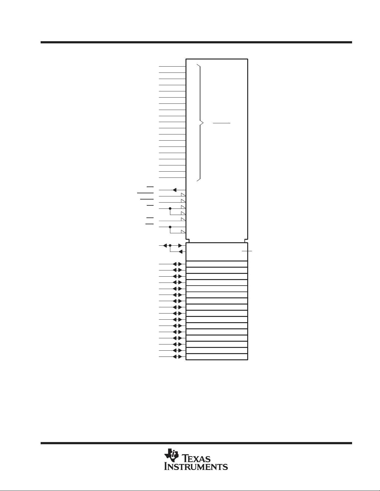
logic symbol for 44-pin package
RY/BY
RESET
†
A0
A1
A2
A3
A4
A5
A6
A7
A8
A9
A10
A11
A12
A13
A14
A15
A16
A17
A18
BYTE
CE
OE
WE
11
10
9
8
7
6
5
4
42
41
40
39
38
37
36
35
34
3
2
1
44
33
12
14
43
0
18
G1
[PWR DWN]
G2 EN (READ)
G3
(WRITE)
FLASH
MEMORY
524288 × 16
A
524287
0
A, 3D
∇ 4
15
DQ0
17
DQ1
19
DQ2
21
DQ3
24
DQ4
26
DQ5
28
DQ6
30
DQ7
16
DQ8
18
DQ9
DQ11
–1
20
22
25
27
29
31
DQ10
DQ12
DQ13
DQ14
DQ15/A
†
This symbol is in accordance with ANSI/IEEE Std 91-1984 and IEC Publication 617-12.
Pin numbers shown are for the DBJ package.
A, Z4
PRODUCT PREVIEW
POST OFFICE BOX 1443 • HOUSTON, TEXAS 77251–1443
5
TMS29LF800T, TMS29LF800B
1048576 BY 8-BIT/524288 BY 16-BIT
FLASH MEMORIES
SMJS828B – SEPTEMBER 1996 – REVISED OCTOBER 1997
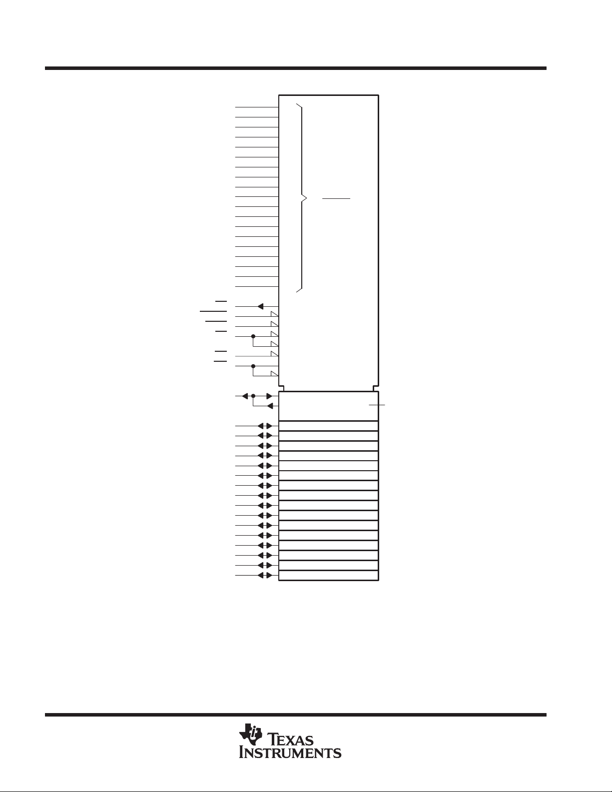
logic symbol for 48-pin package
RY/BY
RESET
†
A0
A1
A2
A3
A4
A5
A6
A7
A8
A9
A10
A11
A12
A13
A14
A15
A16
A17
A18
BYTE
CE
OE
WE
25
24
23
22
21
20
19
18
8
7
6
5
4
3
2
1
48
17
16
15
12
47
26
28
11
0
18
G1
[PWR DWN]
G2 EN (READ)
G3 1, 2 (WRITE)
FLASH
MEMORY
524288 × 16
A
524287
0
A, 3D
∇ 4
29
DQ0
31
DQ1
33
DQ2
35
DQ3
38
DQ4
40
PRODUCT PREVIEW
†
This symbol is in accordance with ANSI/IEEE Std 91-1984 and IEC Publication 617-12.
Pin numbers shown are for the DCD package.
DQ5
DQ6
DQ7
DQ8
DQ9
DQ10
DQ11
DQ12
DQ13
DQ14
DQ15/A
–1
42
44
30
32
34
36
39
41
43
45
A, Z4
6
POST OFFICE BOX 1443 • HOUSTON, TEXAS 77251–1443
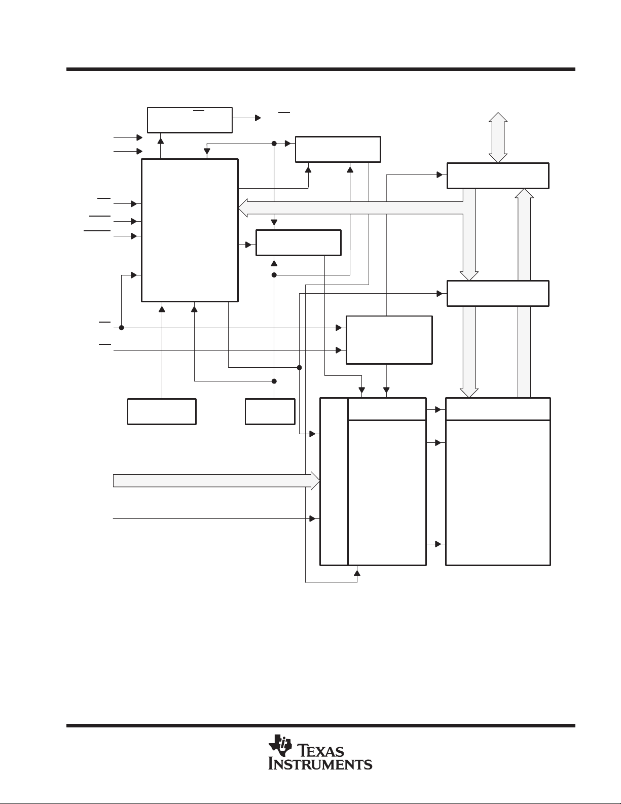
block diagram
V
CC
V
SS
RY/BY
Buffer
TMS29LF800T, TMS29LF800B
1048576 BY 8-BIT/524288 BY 16-BIT
FLASH MEMORIES
SMJS828B – SEPTEMBER 1996 – REVISED OCTOBER 1997
DQ0–DQ15
RY/BY
Erase Voltage
Generator
Input/Output Buffers
WE
BYTE
RESET
A0–A18
CE
OE
State Control
Command Registers
VCC Detector
PGM Voltage
Generator
Timer
STB
STB
Chip-Enable
Output-Enable
Logic
A
d
d
r
e
s
s
Y-Decoder
X-Decoder
Data Latch
Y-Gating
Cell Matrix
PRODUCT PREVIEW
A
–1
POST OFFICE BOX 1443 • HOUSTON, TEXAS 77251–1443
L
a
t
c
h
7
TMS29LF800T, TMS29LF800B
1048576 BY 8-BIT/524288 BY 16-BIT
FLASH MEMORIES
SMJS828B – SEPTEMBER 1996 – REVISED OCTOBER 1997
operation
See Table 1 and Table 2 for the sector-address ranges of the TMS29LF800T/B.
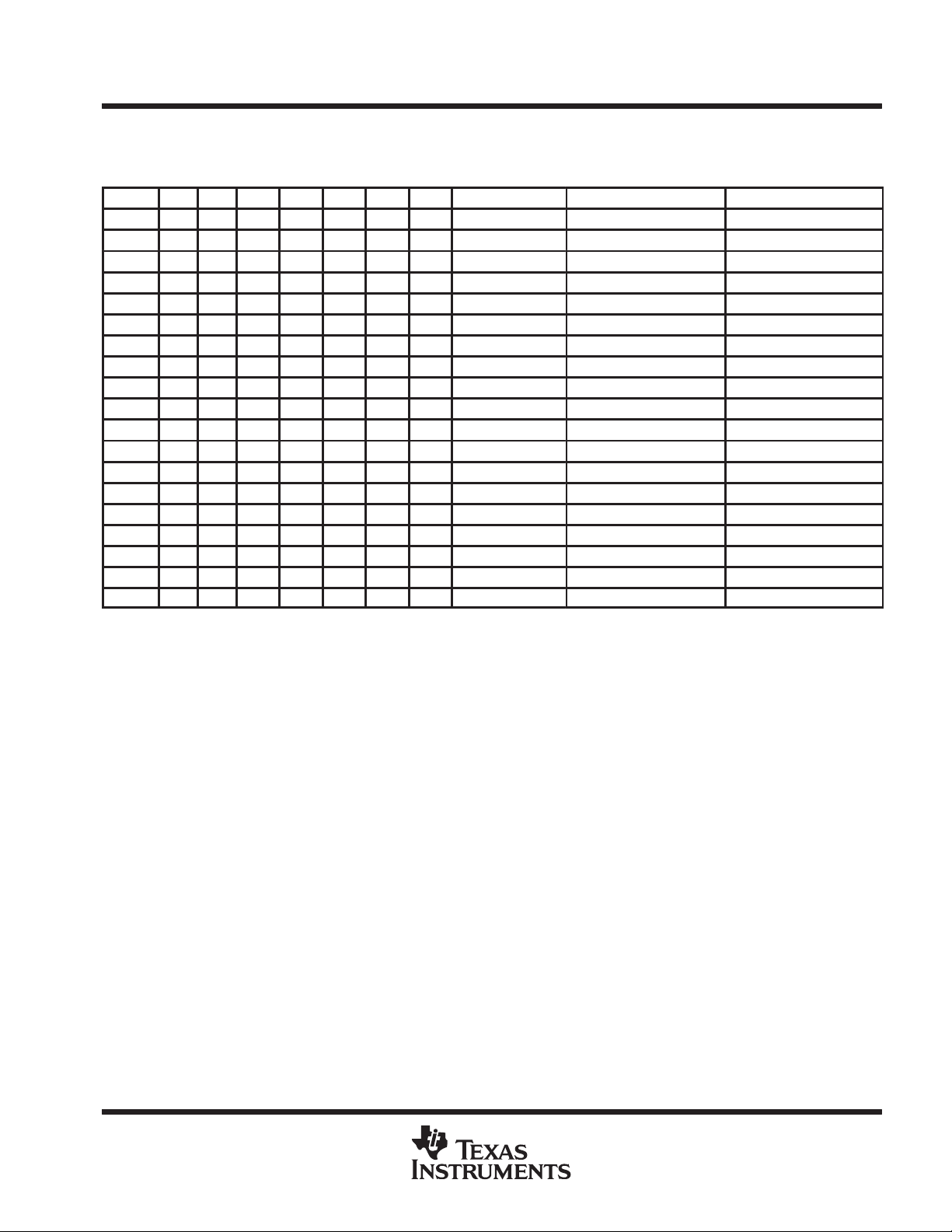
Table 1. Top-Boot Sector-Address Ranges
A18 A17 A16 A15 A14 A13 A12 SECTOR SIZE (x8) ADDRESS RANGE (x16) ADDRESS RANGE
SA18 1 1 1 1 1 1 X 16K-Byte FC000H–FFFFFH 7E000H–7FFFFH
SA17 1 1 1 1 1 0 1 8K-Byte FA000H–FBFFFH 7D000H–7DFFFH
SA16 1 1 1 1 1 0 0 8K-Byte F8000H–F9FFFH 7C000H–7CFFFH
SA15 1 1 1 1 0 X X 32K-Byte F0000H–F7FFFH 78000H–7BFFFH
SA14 1 1 1 0 X X X 64K-Byte E0000H–EFFFFH 70000H–77FFFH
SA13 1 1 0 1 X X X 64K-Byte D0000H–DFFFFH 68000H–6FFFFH
SA12 1 1 0 0 X X X 64K-Byte C0000H–CFFFFH 60000H–67FFFH
SA11 1 0 1 1 X X X 64K-Byte B0000H–BFFFFH 58000H–5FFFFH
SA10 1 0 1 0 X X X 64K-Byte A0000H–AFFFFH 50000H–57FFFH
SA9 1 0 0 1 X X X 64K-Byte 90000H–9FFFFH 48000H–4FFFFH
SA8 1 0 0 0 X X X 64K-Byte 80000H–8FFFFH 40000H–47FFFH
SA7 0 1 1 1 X X X 64K-Byte 70000H–7FFFFH 38000H–3FFFFH
SA6 0 1 1 0 X X X 64K-Byte 60000H–6FFFFH 30000H–37FFFH
SA5 0 1 0 1 X X X 64K-Byte 50000H–5FFFFH 28000H–2FFFFH
SA4 0 1 0 0 X X X 64K-Byte 40000H–4FFFFH 20000H–27FFFH
SA3 0 0 1 1 X X X 64K-Byte 30000H–3FFFFH 18000H–1FFFFH
SA2 0 0 1 0 X X X 64K-Byte 20000H–2FFFFH 10000H–17FFFH
SA1 0 0 0 1 X X X 64K-Byte 10000H–1FFFFH 08000H–0FFFFH
SA0 0 0 0 0 X X X 64K-Byte 00000H–0FFFFH 00000H–07FFFH
†
The address range is A–1–A18 in byte mode.
The address range is A0–A18 in word mode.
†
PRODUCT PREVIEW
8
POST OFFICE BOX 1443 • HOUSTON, TEXAS 77251–1443
operation (continued)
TMS29LF800T, TMS29LF800B
1048576 BY 8-BIT/524288 BY 16-BIT
FLASH MEMORIES
SMJS828B – SEPTEMBER 1996 – REVISED OCTOBER 1997
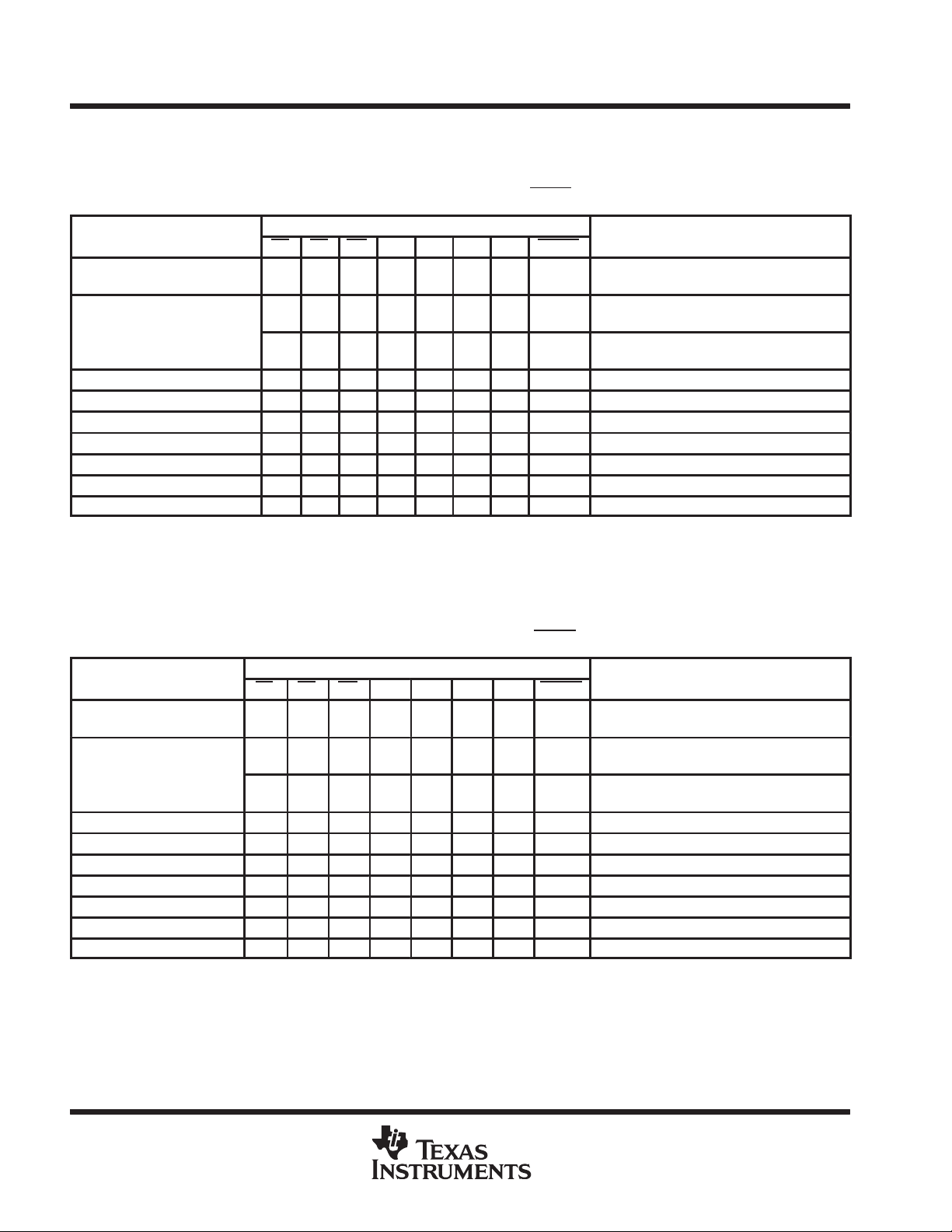
Table 2. Bottom-Boot Sector-Address Ranges
A18 A17 A16 A15 A14 A13 A12 SECTOR SIZE (x8) ADDRESS RANGE (x16) ADDRESS RANGE
SA18 1 1 1 1 X X X 64K-Byte F0000H–FFFFFH 78000H–7FFFFH
SA17 1 1 1 0 X X X 64K-Byte E0000H–EFFFFH 70000H–77FFFH
SA16 1 1 0 1 X X X 64K-Byte D0000H–DFFFFH 68000H–6FFFFH
SA15 1 1 0 0 X X X 64K-Byte C0000H–CFFFFH 60000H–67FFFH
SA14 1 0 1 1 X X X 64K-Byte B0000H–BFFFFH 58000H–5FFFFH
SA13 1 0 1 0 X X X 64K-Byte A0000H–AFFFFH 50000H–57FFFH
SA12 1 0 0 1 X X X 64K-Byte 90000H–9FFFFH 48000H–4FFFFH
SA11 1 0 0 0 X X X 64K-Byte 80000H–8FFFFH 40000H–47FFFH
SA10 0 1 1 1 X X X 64K-Byte 70000H–7FFFFH 38000H–3FFFFH
SA9 0 1 1 0 X X X 64K-Byte 60000H–6FFFFH 30000H–37FFFH
SA8 0 1 0 1 X X X 64K-Byte 50000H–5FFFFH 28000H–2FFFFH
SA7 0 1 0 0 X X X 64K-Byte 40000H–4FFFFH 20000H–27FFFH
SA6 0 0 1 1 X X X 64K-Byte 30000H–3FFFFH 18000H–1FFFFH
SA5 0 0 1 0 X X X 64K-Byte 20000H–2FFFFH 10000H–17FFFH
SA4 0 0 0 1 X X X 64K-Byte 10000H–1FFFFH 08000H–0FFFFH
SA3 0 0 0 0 1 X X 32K-Byte 08000H–0FFFFH 04000H–07FFFH
SA2 0 0 0 0 0 1 1 8K-Byte 06000H–07FFFH 03000H–03FFFH
SA1 0 0 0 0 0 1 0 8K-Byte 04000H–05FFFH 02000H–02FFFH
SA0 0 0 0 0 0 0 X 16K-Byte 00000H–03FFFH 00000H–01FFFH
†
The address range is A–1–A18 in byte mode.
The address range is A0–A18 in word mode.
†
POST OFFICE BOX 1443 • HOUSTON, TEXAS 77251–1443
PRODUCT PREVIEW
9
TMS29LF800T, TMS29LF800B
MODE
DQ0–DQ7
3-V power suppl
MODE
DQ0–DQ15
3-V power suppl
1048576 BY 8-BIT/524288 BY 16-BIT
FLASH MEMORIES
SMJS828B – SEPTEMBER 1996 – REVISED OCTOBER 1997
operation (continued)
See Table 3 and Table 4 for the operation modes of the TMS29LF800T/B.
Table 3. Byte-Operation Mode (BYTE
FUNCTIONS
CE OE WE A0 A1 A6 A9 RESET
Algorithm-selection mode V
p
Read V
Output disable VILVIHV
Standby and write inhibit V
Write‡ VILVIHV
Temporary sector unprotect X X X X X X X V
Verify sector protect V
Hardware reset X X X X X X X V
Legend:
VIL = Logic 0
VIH = Logic 1
VID = 12.0 ± 0.5 V
†
X can be VIL or VIH.
‡
See Table 6 for valid address and data during write.
pp
y
ILVILVIHVILVILVILVID
VILVILVIHVIHVILVILV
VILVILVIHVIHVILVILV
ILVILVIH
X X X X X X V
IH
ILVILVIHVILVIHVILVID
A0 A1 A6 A9 V
X X X X V
IH
A0 A1 A6 A9 V
IL
†
Table 4. Word-Operation Mode (BYTE =VIH)
FUNCTIONS
CE OE WE A0 A1 A6 A9 RESET
V
VILV
Algorithm-selection mode
PRODUCT PREVIEW
p
Read V
Output disable V
Standby and write inhibit V
Write‡ V
Temporary sector unprotect X X X X X X X V
Verify sector protect V
Hardware reset X X X X X X X V
Legend:
VIL = Logic 0
VIH = Logic 1
VID = 12.0 ± 0.5 V
†
X can be VIL or VIH.
‡
See Table 6 for valid address and data during write.
pp
y
IL
V
VILV
IL
V
VILV
IL
VILV
IL
ILVIHVIH
IH
ILVIHVIL
VILV
IL
IHVILVILVILVID
IHVIHVILVILVID
IHVIHVILVILVID
A0 A1 A6 A9 V
IH
X X X X V
X X X X X X V
A0 A1 A6 A9 V
IHVILVIHVILVID
†
= VIL)
Manufacturer-Equivalent Code 01h
V
IH
(TMS29LF800T/B – Byte)
Device-Equivalent Code DAh
V
ID
ID
IH
(TMS29LF800T – Byte)
Device-Equivalent Code 5Bh
V
IH
(TMS29LF800B – Byte)
Data out
IH
Hi-Z
IH
Hi-Z
IH
Data in
IH
X
ID
V
Data out
IH
Hi-Z
IL
V
Manufacturer-Equivalent Code 01h
IH
(TMS29LF800T/B – Word)
V
Device-Equivalent Code 22DAh
IH
(TMS29LF800T – Word)
V
Device-Equivalent Code 225Bh
IH
(TMS29LF800B – Word)
Data out
IH
Hi-Z
IH
Hi-Z
IH
Data in
IH
X
ID
V
Data out
IH
Hi-Z
IL
10
POST OFFICE BOX 1443 • HOUSTON, TEXAS 77251–1443
read mode
TMS29LF800T, TMS29LF800B
1048576 BY 8-BIT/524288 BY 16-BIT
FLASH MEMORIES
SMJS828B – SEPTEMBER 1996 – REVISED OCTOBER 1997
A logic-low signal applied to the CE
and OE pins allows the output of the TMS29LF800T/B to be read. When
two or more ’29LF800T/B devices are connected in parallel, the output of any one device can be read without
interference. The CE
pin is for power control and is used for device selection. The OE pin is for output control,
and is used to gate the data output onto the bus from the selected device.
The address-access time (t
access time (t
access time (t
) is the delay from CE low and stable addresses to valid output data. The output-enable
ELQV
) is the delay from OE low to valid output data when CE equals logic low and addresses are
GLQV
stable for at least the duration of t
) is the delay from stable address to valid output data. The chip-enable (CE)
AVQV
AVQV–tGLQV
.
standby mode
I
supply current is reduced by applying a logic-high level on CE and RESET to enter the standby mode. In
CC
the standby mode, the outputs are placed in the high-impedance state. Applying a CMOS logic-high level on
CE
and RESET reduces the current to 60 µA. Applying a TTL logic-high level on CE and RESET reduces the
current to 1 mA. If the ’29LF800T/B is deselected during erasure or programming, the device continues to draw
active current until the operation is complete.
output disable
When OE
equals VIH or CE equals VIH, output from the device is disabled and the output pins (DQ0–DQ15) are
placed in the high-impedance state.
automatic-sleep mode
The ’29LF800T/B has a built-in feature called automatic-sleep mode to minimize device energy consumption
which is independent of CE
, WE, and OE, and is enabled when addresses remain stable for 300 ns. Typical
sleep-mode current is 60 µA. Sleep mode does not affect output data, which remains latched and available to
the system.
algorithm selection
The algorithm-selection mode provides access to a binary code that matches the device with its proper
programming and erase command operations. This mode is activated when V
address pin A9. Address pins A1 and A6 must be logic low. T wo bytes of code are accessed by toggling address
pin A0 from V
to VIH. Address pins other than A0, A1, and A6 can be at logic low or at logic high.
IL
The algorithm-selection mode can also be read by using the command register, which is useful when V
available to be placed on address pin A9. Table 5 shows the binary algorithm-selection codes.
Table 5. Algorithm-Selection Codes (3-V Single Power Supply)
CODE DQ15 DQ14 DQ13 DQ12 DQ11 DQ10 DQ9 DQ8 DQ7 DQ6 DQ5 DQ4 DQ3 DQ2 DQ1 DQ0
Manufacturerequivalent code
TMS29LF800T Byte
TMS29LF800BByte
TMS29LF800T 22DAH 0 0 1 0 0 0 1 0 1 1 0 1 1 0 1 0
TMS29LF800B 225BH 0 0 1 0 0 0 1 0 0 1 0 1 1 0 1 1
Sector protection 01H 0 0 0 0 0 0 0 0 0 0 0 0 0 0 0 1
†
A1 = VIL, A6 = VIL, CE = VIL, OE = V
01H 0 0 0 0 0 0 0 0 0 0 0 0 0 0 0 1
DAH A
5BH A
Hi-Z Hi-Z Hi-Z Hi-Z Hi-Z Hi-Z Hi-Z 1 1 0 1 1 0 1 0
–1
Hi-Z Hi-Z Hi-Z Hi-Z Hi-Z Hi-Z Hi-Z 0 1 0 1 1 0 1 1
–1
IL
(1 1.5 V to 12.5 V) is placed on
ID
ID
†
PRODUCT PREVIEW
is not
POST OFFICE BOX 1443 • HOUSTON, TEXAS 77251–1443
11

TMS29LF800T, TMS29LF800B
1048576 BY 8-BIT/524288 BY 16-BIT
FLASH MEMORIES
SMJS828B – SEPTEMBER 1996 – REVISED OCTOBER 1997
erasure and programming
Erasure and programming of the ’29LF800 are accomplished by writing a sequence of commands using
standard microprocessor write timing. The commands are written to a command register and input to the
command-state machine (CSM). The CSM interprets the command entered and initiates program, erase,
suspend, and resume operations as instructed. The CSM acts as the interface between the write-state machine
(WSM) and external-chip operations. The WSM controls all voltage generation, pulse generation,
preconditioning, and verification of memory contents. Program and block-/chip-erase functions are fully
automatic. Once the end of a program or erase operation has been reached, the device resets internally to the
read mode. If V
aborted and subsequent writes are ignored until the V
logically correct to prevent unintentional command writes, programming, or erasing.
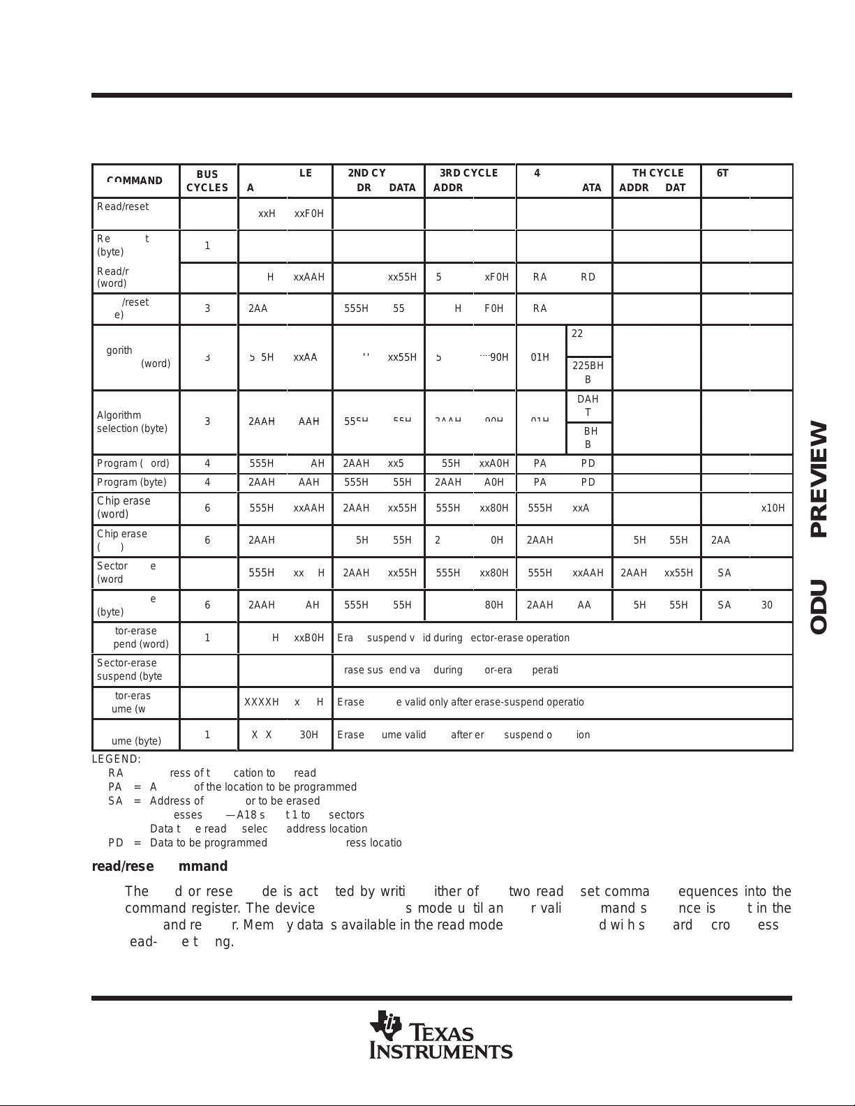
command definitions
Device operating modes are selected by writing specific address and data sequences into the command
register. Table 6 defines the valid command sequences. Writing incorrect address and data values or writing
them in the incorrect sequence causes the device to reset to the read mode. The command register does not
occupy an addressable memory location. The register is used to store the command sequence along with the
address and data needed by the memory array. Commands are written by setting CE
bringing WE
on the rising edge of WE
characteristics of the write/erase/program-operations section for specific timing information.
drops below the low-voltage-detect level (V
CC
from logic high to logic low. Addresses are latched on the falling edge of WE and data is latched
. Holding WE = VIL and toggling CE is an alternative method. See the switching
level is greater than V
CC
), any programming or erase operation is
LKO
. The control pins must be
LKO
= VIL, OE = VIH, and
PRODUCT PREVIEW
12
POST OFFICE BOX 1443 • HOUSTON, TEXAS 77251–1443
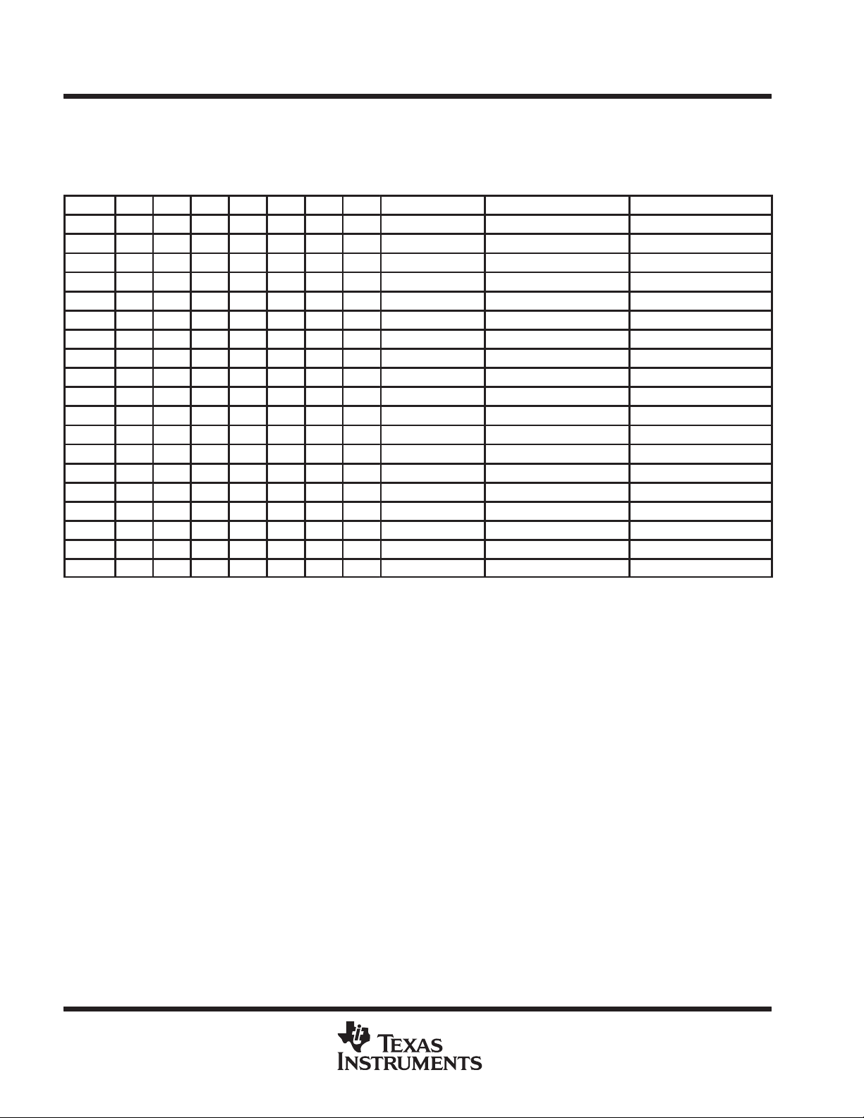
command definitions (continued)
COMMAND
Á
Á
Á
Á
Á
Á
Á
Á
Á
Á
Á
Á
Á
Á
Á
Á
Á
go
Á
3
Á
555H
Á
AAH
Á
2AAH
Á
55H
Á
555H
Á
90H
Á
01H
Á
Á
Á
g
Á
3
Á
2AAH
Á
AAH
Á
555H
Á
55H
Á
2AAH
Á
90H
Á
01H
Á
Á
Á
Á
Á
Á
Á
Á
Á
Á
Á
Á
Á
Á
Á
Á
Á
Á
Á
Á
Á
Á
Á
Á
Á
Á
Á
Á
Á
Á
Á
Á
Á
Á
Á
Á
Á
Á
Á
Á
Á
Á
Á
Á
Á
Á
Á
Á
Á
Á
Á
Á
Á
Á
Á
Á
Á
Á
Á
TMS29LF800T, TMS29LF800B
1048576 BY 8-BIT/524288 BY 16-BIT
FLASH MEMORIES
SMJS828B – SEPTEMBER 1996 – REVISED OCTOBER 1997
Table 6. Command Definitions
Read/reset
(word)
Read/reset
(byte)
ÁÁÁ
Read/reset
(word)
Read/reset
(byte)
ÁÁÁ
Algorithm
selection (word)
ÁÁÁ
BUS
CYCLES
1
1
ÁÁ
3
3
ÁÁ
ÁÁ
1ST CYCLE
ADDR
xxxxH
xxx
Á
555H
2AAH
Á
Á
DATA
xxF0H
F0H
Á
xxAAH
AAH
Á
xx
Á
2ND CYCLE
ADDR
ÁÁÁÁÁÁÁÁÁÁÁÁÁÁÁÁÁÁÁÁ
2AAH
555H
Á
Á
Algorithm
selection (byte)
ÁÁÁ
Program (word)
Program (byte)
Chip erase
ÁÁÁ
(word)
Chip erase
(byte)
Sector erase
ÁÁÁ
(word)
Sector erase
(byte)
ÁÁÁ
Sector-erase
ÁÁÁ
suspend (word)
Sector-erase
suspend (byte)
ÁÁÁ
Sector-erase
resume (word)
Sector-erase
resume (byte)
ÁÁÁ
ÁÁ
4
4
6
ÁÁ
6
6
ÁÁ
6
ÁÁ
1
ÁÁ
1
ÁÁ
1
1
ÁÁ
Á
555H
2AAH
555H
Á
2AAH
555H
Á
2AAH
Á
XXXXH
Á
XXX
Á
XXXXH
XXX
Á
Á
xxAAH
AAH
xxAAH
Á
AAH
xxAAH
Á
AAH
Á
xxB0H
Á
B0H
Á
xx30H
30H
Á
Á
2AAH
555H
2AAH
Á
555H
2AAH
Á
555H
Á
Erase suspend valid during sector-erase operation
ББББББББББББББББББББ
Erase suspend valid during sector-erase operation
ББББББББББББББББББББ
Erase resume valid only after erase-suspend operation
Erase resume valid only after erase-suspend operation
ББББББББББББББББББББ
LEGEND:
RA = Address of the location to be read
PA = Address of the location to be programmed
SA = Address of the sector to be erased
Addresses A12—A18 select 1 to 19 sectors.
RD = Data to be read at selected address location
PD = Data to be programmed at selected address location
DATA
xx55H
55H
Á
xx
Á
Á
xx55H
55H
xx55H
Á
55H
xx55H
Á
55H
Á
3RD CYCLE
ADDR
555H
2AAH
ÁÁ
ÁÁ
ÁÁ
555H
2AAH
555H
ÁÁ
2AAH
555H
ÁÁ
2AAH
ÁÁ
DATA
xxF0H
F0H
Á
xx
Á
Á
xxA0H
A0H
xx80H
Á
80H
xx80H
Á
80H
Á
4TH CYCLE
ADDR
RA
RA
Á
Á
Á
PA
PA
555H
Á
2AAH
555H
Á
2AAH
Á
DATA
RD
RD
Á
22DAH
T
225BH
B
Á
DAH
T
5BH
B
Á
PD
PD
xxAAH
Á
AAH
xxAAH
Á
AAH
Á
5TH CYCLE
ADDR
ÁÁÁÁÁÁÁ
ÁÁÁÁÁÁÁ
ÁÁÁÁÁÁÁ
2AAH
Á
555H
2AAH
Á
555H
Á
DATA
xx55H
Á
55H
xx55H
Á
55H
Á
6TH CYCLE
ADDR
555H
Á
2AAH
SA
Á
SA
Á
Á
Á
Á
DATA
xx10H
10H
xx30H
30H
PRODUCT PREVIEW
read/reset command
The read or reset mode is activated by writing either of the two read/reset command sequences into the
command register. The device remains in this mode until another valid command sequence is input in the
command register. Memory data is available in the read mode and can be read with standard microprocessor
read-cycle timing.
POST OFFICE BOX 1443 • HOUSTON, TEXAS 77251–1443
13

TMS29LF800T, TMS29LF800B
1048576 BY 8-BIT/524288 BY 16-BIT
FLASH MEMORIES
SMJS828B – SEPTEMBER 1996 – REVISED OCTOBER 1997
read/reset command (continued)
On power up, the device defaults to the read/reset mode. A read/reset command sequence is not required and
memory data is available.
algorithm-selection command
The algorithm-selection command allows access to a binary code that matches the device with the proper
programming and erase command operations. After writing the three-bus-cycle command sequence, the first
byte/word of the algorithm-selection code can be read from address XX00h. The second byte/word of the code
can be read from address XX01h (see Table 6). This mode remains in effect until another valid command
sequence is written to the device.
program command
Programming is a four-bus-cycle command sequence. The first three bus cycles put the device into the
program-setup state. The fourth bus cycle loads the address location and the data to be programmed into the
device. The addresses are latched on the falling edge of WE
in the fourth bus cycle. The rising edge of WE starts the program operation. The embedded programming
function automatically provides needed voltage and timing to program and verify the cell margin. Any further
commands written to the device during the program operation are ignored.
Programming can be performed at any address location in any sequence. When erased, all bits are in a
logic-high state. Logic lows are programmed into the device and only an erase operation can change bits from
logic lows to logic highs. Attempting to program a 1 into a bit that has been programmed previously to a 0 causes
the internal-pulse counter to exceed the pulse-count limit, which sets the exceed-time-limit indicator (DQ5) to
a logic-high state. The automatic-programming operation is complete when the data on DQ7 is equivalent to
the data written to DQ5, at which time the device returns to the read mode and addresses are no longer latched.
Figure 9 shows a flowchart of the typical device-programming operation.
and the data is latched on the rising edge of WE
chip-erase command
Chip erase is a six-bus-cycle command sequence. The first three bus cycles put the device into the erase-setup
state. The next two bus cycles unlock the erase mode. The sixth bus cycle loads the chip-erase command. This
command sequence is required to ensure that the memory contents are not erased accidentally . The rising edge
of WE
starts the chip-erase operation. Any further commands written to the device during the chip-erase
operation are ignored.
PRODUCT PREVIEW
The embedded chip-erase function automatically provides voltage and timing needed to program and to verify
all the memory cells prior to electrical erase. It then erases and verifies the cell margin automatically without
programming the memory cells prior to erase.
Figure 12 shows a flowchart of the typical chip-erase operation.
sector-erase command
Sector-erase is a six-bus-cycle command sequence. The first three bus cycles put the device into the
erase-setup state. The next two bus cycles unlock the erase mode and then the sixth bus cycle loads the
sector-erase command and the sector-address location to be erased. Any address location within the desired
sector can be used. The addresses are latched on the falling edge of WE
is latched on the rising edge of WE
sector-erase operation begins on the selected sector(s).
Additional sectors can be selected to be erased concurrently during the sector-erase command sequence. For
each additional sector to be selected for erase, another bus cycle is issued. The bus cycle loads the next
sector-address location and the sector-erase command. The time between the end of the previous bus cycle
and the start of the next bus cycle must be less than 100 µs; otherwise, the new sector location is not loaded.
A time delay of 100 µs from the rising edge of the last WE
edge of WE
within the 100 µs time delay, the timer is reset.
and the sector-erase command (30h)
in the sixth bus cycle. After a delay of 80 µs from the rising edge of WE, the
starts the sector-erase operation. If there is a falling
14
POST OFFICE BOX 1443 • HOUSTON, TEXAS 77251–1443

TMS29LF800T, TMS29LF800B
1048576 BY 8-BIT/524288 BY 16-BIT
FLASH MEMORIES
SMJS828B – SEPTEMBER 1996 – REVISED OCTOBER 1997
sector-erase command (continued)
One to nineteen sector-address locations can be loaded in any sequence. The state of the delay timer can be
monitored using the sector-erase delay indicator (DQ3). If DQ3 is at logic low, the time delay has not expired.
See the operation status section for a description.
Any command other than erase suspend (B0h) or sector erase (30h) written to the device during the
sector-erase operation causes the device to exit the sector-erase mode and the contents of the sector(s)
selected for erase are no longer valid. To complete the sector-erase operation, reissue the sector-erase
command sequence.
The embedded sector-erase function automatically provides needed voltage and timing to program and to verify
all of the memory cells prior to electrical erase and then erases and verifies the cell margin automatically.
Programming the memory cells prior to erase is not required.
See the operation status section for a full description. Figure 14 shows a flowchart of the typical sector-erase
operation.
erase-suspend command
The erase-suspend command (B0h) allows interruption of a sector-erase operation to read data from unaltered
sectors of the device. Erase-suspend is a one-bus-cycle command. The addresses can be V
erase-suspend command (B0h) is latched on the rising edge of WE
progress, the erase-suspend command requests the internal write-state machine to halt operation at
predetermined breakpoints. The erase-suspend command is valid only during the sector-erase operation and
is invalid during programming and chip-erase operations. The sector-erase delay timer expires immediately if
the erase-suspend command is issued while the delay is active.
. Once the sector-erase operation is in
or VIH and the
IL
After the erase-suspend command is issued, the device takes between 0.1 µs and 15 µs to suspend the
operation. The toggle bit must be monitored to determine when the suspend has been executed. When the
toggle bit stops toggling, data can be read from sectors that are not selected for erase. Reading from a sector
selected for erase can result in invalid data. See the operation status section for a full description.
Once the sector-erase operation is suspended, reading from or programing to a sector that is not being erased
can be performed. This command is applicable only during sector-erase operation. Any other command written
during erase-suspend mode to the suspended sector is ignored.
erase-resume command
The erase-resume command (30h) restarts a suspended sector-erase operation from the point where it was
halted. Erase resume is a one-bus-cycle command. The addresses can be V
command (30h) is latched on the rising edge of WE
combination is written, the internal-pulse counter (exceed timing limit) is reset. The erase-resume command
is valid only in the erase-suspend state. After the erase-resume command is executed, the device returns to
the valid sector-erase state and further writes of the erase-resume command are ignored. After the device has
resumed the sector-erase operation, another erase-suspend command can be issued to the device.
. When an erase-suspend/erase-resume command
or VIH and the erase-resume
IL
operation status
The status of the device during an automatic-programming algorithm, chip-erase, or automatic-erase algorithm
can be determined in three ways:
D
DQ7: Data polling
D
DQ6: Toggle bit
PRODUCT PREVIEW
D
RY/BY: Ready/busy bit
POST OFFICE BOX 1443 • HOUSTON, TEXAS 77251–1443
15

TMS29LF800T, TMS29LF800B
Erase-suspend mode
1048576 BY 8-BIT/524288 BY 16-BIT
FLASH MEMORIES
SMJS828B – SEPTEMBER 1996 – REVISED OCTOBER 1997
status-bit definitions
During operation of the automatic embedded program and erase functions, the status of the device can be
determined by reading the data state of designated outputs. The data-polling bit (DQ7) and toggle bit (DQ6)
require multiple successive reads to observe a change in the state of the designated output. Table 7 defines
the values of the status flags.
Table 7. Operation Status Flags
DEVICE OPERATION
Programming DQ7 T 0 0 No Tog 0
Program/erase in auto-erase 0 T 0 1
In progress
Program in erase suspend DQ7
Programming DQ7 T 1 0 No Tog 0
Exceeded time limits
Successful operation
complete
†
T= toggle, D= data, No Tog= No toggle
‡
DQ4, DQ1, DQ0 are reserved for future use.
§
DQ2 can be toggled when the sector address applied is an erasing sector. DQ2 cannot be toggled when the sector address applied is a
non-erasing sector. DQ2 is used to determine which sectors are erasing and which are not.
¶
Status flags apply when outputs are read from the address of a non-erase-suspend operation.
#
If DQ5 is high (exceeded timing limits), successive reads from a problem sector causes DQ2 to toggle.
Program/erase in auto erase 0 T 1 1
Program in erase suspend DQ7 T 1 0 No Tog 0
Programming complete D D D D D 1
Sector-/chip-erase complete 1 1 1 1 1 1
p
Erase-sector address 1 No Tog 0 0 T 1
Non-erase sector address D D D D D 1
‡
†
DQ7 DQ6 DQ5 DQ3 DQ2 RY/BY
§
¶
T 0 0 1
§
#
data-polling (DQ7)
The data-polling-status function outputs the complement of the data latched into the DQ7 data register while
the write-state machine (WSM) is engaged in a program or erase operation. Data bit DQ7 toggling from
complement to true indicates the end of an operation. Data-polling is available only during programming,
chip-erase, sector-erase, and sector-erase-timing delay . Data-polling is valid after the rising edge of WE
last bus cycle of the command sequence loaded into the command register. Figure 16 shows a flowchart for
PRODUCT PREVIEW
data-polling.
During a program operation, reading DQ7 outputs the complement of the DQ7 data to be programmed at the
selected address location. Upon completion, reading DQ7 outputs the true DQ7 data loaded into the
program-data register. During erase operations, reading DQ7 outputs a logic low. Upon completion, reading
DQ7 outputs a logic high. Also, data-polling must be performed at a sector address that is within a sector that
is being erased; otherwise, the status is invalid. When using data-polling, the address should remain stable
throughout the operation.
0
0
0
in the
During a data-polling read, while OE
read timing, the system can read valid data on DQ7, while other DQ pins are still invalid. A subsequent read
of the device is valid. See Figure 17 for the data-polling timing diagram.
toggle bit (DQ6)
The toggle-bit status function outputs data on DQ6, which toggles between logic high and logic low while the
WSM is engaged in a program or erase operation. When DQ6 stops toggling after two consecutive reads to the
same address, the operation is complete. The toggle bit is available only during programming, chip erase, sector
erase, and sector-erase-timing delay. Toggle-bit data is valid after the rising edge of WE
of the command sequence loaded into the command register. Figure 18 shows a flowchart of the toggle-bit
status-read algorithm. Depending on the read timing, DQ6 can stop toggling while other DQ pins are still invalid
and a subsequent read of the device is valid. See Figure 19 for the toggle-bit timing diagram.
16
is logic low, data bit DQ7 can change asynchronously. Depending on the
in the last bus cycle
POST OFFICE BOX 1443 • HOUSTON, TEXAS 77251–1443

TMS29LF800T, TMS29LF800B
1048576 BY 8-BIT/524288 BY 16-BIT
FLASH MEMORIES
SMJS828B – SEPTEMBER 1996 – REVISED OCTOBER 1997
exceed time limit (DQ5)
Program and erase operations use an internal-pulse counter to limit the number of pulses applied. If the
pulse-count limit is exceeded, DQ5 is set to a logic-high data state. This indicates that the program or erase
operation has failed. DQ7 does not change from complemented data to true data and DQ6 does not stop
toggling when read. To continue operation, the device must be reset.
The exceed-time-limit condition occurs when attempting to program a logic-high state into a bit that has been
programmed previously to a logic low. Only an erase operation can change bits from logic low to logic high. After
reset, the device is functional and can be erased and reprogrammed.
sector-load-timer (DQ3)
The sector-load-timer status bit, DQ3, is used to determine whether the time to load additional sector addresses
has expired. After completion of a sector-erase command sequence, DQ3 remains at a logic low for 100 µs.
This indicates that another sector-erase command sequence can be issued. If DQ3 is at a logic high, it indicates
that the delay has expired and attempts to issue additional sector-erase commands are ignored. See the
sector-erase command section for a description.
The data-polling and toggle bit are valid during the 100-µs time delay and can be used to determine if a valid
sector-erase command has been issued. To ensure additional sector-erase commands have been accepted,
the status of DQ3 should be read before and after each additional sector-erase command. If DQ3 is at a logic
low on both reads, the additional sector-erase command was accepted.
toggle bit 2 (DQ2)
The state of DQ2 determines whether the device is in algorithmic-erase mode or erase-suspend mode. DQ2
toggles if successive reads are issued to the erasing or erase-suspended sector, assuming in case of the latter
that the device is in erase-suspend-read mode. DQ2 also toggles when DQ5 becomes a logic high due to the
timer exceeding the time limit, and reads are issued to the failed sector. DQ2 does not toggle in any other sector
due to DQ5 failure. When the device is in erase-suspend-program mode, successive reads from the
non-erase-suspended sector causes a logic high on DQ2.
ready/busy bit (RY/BY
The RY/BY
If the RY/BY
not accept any other commands except for erase suspend. While it is in the erase-suspend mode, RY / BY
remains high. In program mode, the RY/BY bit is valid (logic low) after the fourth WE pulse. In erase mode, it
is valid after the sixth WE
timing waveform.
Since the RY/BY
to V
CC
hardware-reset bit (RESET
When the RESET
state. It also avoids bus contention by placing the outputs into the high-impedance state for the duration of the
RESET
During a program or erase operation, if RESET
the reset operation is complete. Since this can take from 1 µs to 20 µs, the RY/BY
completion or the user can allow a maximum of 20 µs. If RESET
operation is complete within 500 ns. See Figure 1 and Figure 2 for timing specifications.
bit indicates when the device can accept new commands after performing algorithmic operations.
.
pulse.
)
(open-drain output) bit is low, the device is busy with either a program or erase operation and does
pulse. After a delay period, t
bit is an open-drain output, several such bits can be combined in parallel with a pullup resistor
)
pin is driven to a logic low, it forces the device out of the currently active mode and into a reset
is asserted to logic low, the R Y/BY bit remains at logic low until
, the RY/BY bit becomes valid. See Figure 28 for the
busy
bit can be used to sense reset
is asserted during read mode, then the reset
PRODUCT PREVIEW
The RESET
V
± 0.3 V to it. I
SS
anytime, regardless of the condition of CE
pin can also be used to drive the device into deep power-down (standby) mode by applying
reads <1 µA typical, and 5 µA maximum for CMOS inputs. Standby mode can be entered
CC4
POST OFFICE BOX 1443 • HOUSTON, TEXAS 77251–1443
.
17

TMS29LF800T, TMS29LF800B
1048576 BY 8-BIT/524288 BY 16-BIT
FLASH MEMORIES
SMJS828B – SEPTEMBER 1996 – REVISED OCTOBER 1997
hardware-reset bit (RESET) (continued)
Asserting RESET
during program or erase can leave erroneous data in the address locations. These locations
need to be updated after the device resumes normal operations. A minimum of 50 ns must be allowed after
RESET
RESET
RY/BY
goes high before a valid read can take place.
tRL = 500 ns
20 µs max
Figure 1. Device Reset During a Program or Erase Operation
tRL = 500 ns
RESET
RY/BY
0 V
Figure 2. Device Reset During Read Mode
PRODUCT PREVIEW
18
POST OFFICE BOX 1443 • HOUSTON, TEXAS 77251–1443

word-/byte-mode configuration
TMS29LF800T, TMS29LF800B
1048576 BY 8-BIT/524288 BY 16-BIT
FLASH MEMORIES
SMJS828B – SEPTEMBER 1996 – REVISED OCTOBER 1997
The BYTE
all data outputs valid and the DQ15/A
is in byte mode with only DQ0–DQ7 valid. The remaining outputs are in high-impedance mode and DQ15/A
pin is used to set the device configuration. If BYTE is at a logic 1, the device is in word mode with
output representing DQ15. Similarly , if BYTE is at a logic 0, the device
–1
–1
is used as an input for the least significant bit (A1) address function. See Figure 3 and Figure 4 for timing
specifications.
CE
OE
t
ELFH
BYTE
DQ8 –DQ14
DQ15/A –1
DQ8 –DQ14 DQ8 –DQ14
t
FHQV
A –1 DQ15
Figure 3. Word-Mode Configuration
CE
OE
t
ELFL
BYTE
DQ8–DQ14
DQ15/A–1
DQ8–DQ14 DQ8–DQ14
t
FLQV
DQ15
A–1
Figure 4. Byte-Mode Configuration
temporary hardware-sector unprotect feature
This feature temporarily enables both programming and erase operations on any combination of one to nineteen
sectors that were previously protected. The unprotect feature is enabled using high voltage V
12.5 V) on the RESET
pin, using standard command sequences.
ID
Normally, the device is delivered with all sectors unprotected.
PRODUCT PREVIEW
(11.5 V to
POST OFFICE BOX 1443 • HOUSTON, TEXAS 77251–1443
19

TMS29LF800T, TMS29LF800B
1048576 BY 8-BIT/524288 BY 16-BIT
FLASH MEMORIES
SMJS828B – SEPTEMBER 1996 – REVISED OCTOBER 1997
sector-protect programming
The sector-protect programming mode is activated when A6, A0, and CE
control pin OE
are forced to VID. Address pin A1 is set to VIH.The sector-select address pins A12–A18 are used
are at VIL, and address pin A9 and
to select the sector to be protected. Address pins A0–A1 1 and I/O pins must be stable and can be either V
V
. Once the addresses are stable, WE is pulsed low for 100 µs, causing programming to begin on the falling
IH
edge of WE
and to terminate on the rising edge of WE. Figure 20 is a flowchart of the sector-protect algorithm
and Figure 21 shows a timing diagram of the sector-protect operation.
Commands to program or erase a protected sector do not change the data contained in the sector. Attempts
to program and erase a protected sector cause the data-polling bit (DQ7), and the toggle bit (DQ6) to operate
from 2 µs to 100 µs and then return to valid data.
sector-protect verify
Verification of sector-protection programming is accomplished when WE
pin A9 = V
, and then address pins A0 and A6 are set to VIL and A1 is set to VIH. Sector-address pins A12–A18
ID
select the sector that is to be verified. The other addresses can be V
= VIH, OE = VIL, CE = VIL, and address
or VIL. If the selected sector is protected,
IH
the DQs output 01h. If the sector is not protected, the DQs output 00h.
Sector-protect verify can also be read using the algorithm-selection command. After issuing the three-bus-cycle
command sequence, the sector-protection status can be read on DQ0. Set address pins A0 = V
and A6 = V
are set to V
, and then sector address pins A12–A18 select the sector to be verified. The remaining addresses
IL
. If the sector selected is protected, DQ0 outputs a logic-high state. If the sector selected is not
IL
protected, DQ0 outputs a logic-low state. This mode remains in effect until another valid command sequence
is written to the device. Figure 20 is a flowchart of the sector-protect algorithm and Figure 21 shows a timing
diagram of the sector-protect operation.
sector unprotect
, A1 = VIH,
IL
or
IL
Prior to sector unprotect, all sectors must be protected using the sector-protect programming mode. Sector
unprotect is activated when address pin A9 and control pin OE
set to V
while CE and A0 are set to VIL. The sector-select address pins A12–A18 can be VIL or VIH. All sectors
IH
are unprotected in parallel and once the inputs are stable, WE
operation to begin on the falling edge of WE
of the sector-unprotect algorithm and Figure 23 shows a timing diagram of the sector-unprotect operation.
sector-unprotect verify
PRODUCT PREVIEW
Verification of sector unprotect is accomplished when WE
the sector to be verified. Address pins A1 and A6 are set to V
be V
or VIL. If the sector selected is protected, the DQs output 01h. If the sector is not protected, the DQs output
IH
00h. Sector unprotect can also be read using the algorithm-selection command.
low V
write lockout
CC
During power-up and power-down operations, write cycles are locked out for V
the command input is disabled and the device is reset to the read mode. On power up, if CE
and OE
= VIH, the device does not accept commands on the rising edge of WE. The device automatically powers
up in the read mode.
glitching
Pulses of less than 5 ns (typical) on OE
power supply considerations
Each device should have a 0.1-µF ceramic capacitor connected between V
Printed circuit traces to V
should be appropriate to handle the current demand and minimize inductance.
CC
are forced to VID. Address pins A1 and A6 are
is pulsed low for 10 ms, causing the unprotect
and to terminate on the rising edge of WE. Figure 22 is a flowchart
= VIH, OE = VIL, CE =VIL, and A9 = VID, and then select
, and A0 is set to VIL. The other addresses can
IH
less than V
CC
. If VCC < V
LKO
= VIL, WE = VIL,
, WE, or CE do not issue a write cycle.
and VSS to suppress circuit noise.
CC
LKO
,
20
POST OFFICE BOX 1443 • HOUSTON, TEXAS 77251–1443

TMS29LF800T, TMS29LF800B
VIHHigh-level dc input voltage
V
VILLow-level dc input voltage
V
1048576 BY 8-BIT/524288 BY 16-BIT
FLASH MEMORIES
SMJS828B – SEPTEMBER 1996 – REVISED OCTOBER 1997
absolute maximum ratings over ambient temperature range (unless otherwise noted)
Supply voltage range, V
Input voltage range: All inputs except A9, CE
Output voltage range (see Note 3) –0.6 V to V
Ambient temperature range during read/erase/program, T
(see Note 1) –0.6 V to 7 V. . . . . . . . . . . . . . . . . . . . . . . . . . . . . . . . . . . . . . . . . . . . . .
CC
, OE (see Note 2) –0.6 V to VCC + 1 V. . . . . . . . . . . . . . . . . . . .
A9, CE
, OE –0.6 V to 13.5 V. . . . . . . . . . . . . . . . . . . . . . . . . . . . . . . . . . . . . . . . . . . . . . . . . .
A
†
+ 1 V. . . . . . . . . . . . . . . . . . . . . . . . . . . . . . . . . . . . . . . . . . . .
CC
(L) 0°C to 70°C. . . . . . . . . . . . . . . . . . . . . . . . . . . . . . . . . . . . . . . . . . . . . . . . . . .
(E) –40°C to 85°C. . . . . . . . . . . . . . . . . . . . . . . . . . . . . . . . . . . . . . . . . . . . . . . .
(Q) –40°C to 125°C. . . . . . . . . . . . . . . . . . . . . . . . . . . . . . . . . . . . . . . . . . . . . . .
Storage temperature range, T
†
Stresses beyond those listed under “absolute maximum ratings” may cause permanent damage to the device. These are stress ratings only, and
functional operation of the device at these or any other conditions beyond those indicated under “recommended operating conditions” is not
implied. Exposure to absolute-maximum-rated conditions for extended periods may affect device reliability.
NOTES: 1. All voltage values are with respect to VSS.
2. The voltage on any input pin can undershoot to –2 V for periods less than 20 ns (see Figure 6).
3. The voltage on any input or output pin can overshoot to 7 V for periods less than 20 ns (see Figure 7).
–65°C to 150°C. . . . . . . . . . . . . . . . . . . . . . . . . . . . . . . . . . . . . . . . . . . . . . . . . .
stg
recommended operating conditions
MIN MAX UNIT
V
V
V
T
Supply voltage 2.7 3.6 V
CC
p
p
Algorithm selection and sector-protect input voltage 11.5 12.5 V
ID
Low VCC lock-out voltage 2.3 2.5 V
LKO
Ambient temperature
A
TTL 2 VCC+0.5
CMOS VCC–0.5 VCC+0.5
TTL –0.5 0.8
CMOS –0.5 0.8
L version 0 70
E version –40 85
Q version –40 125
°C
POST OFFICE BOX 1443 • HOUSTON, TEXAS 77251–1443
PRODUCT PREVIEW
21

TMS29LF800T, TMS29LF800B
VOHHigh-level output voltage
V
I
pply current (standby)
I
CC
y
CE
V
V
mA
1048576 BY 8-BIT/524288 BY 16-BIT
FLASH MEMORIES
SMJS828B – SEPTEMBER 1996 – REVISED OCTOBER 1997
electrical characteristics over recommended ranges of supply voltage and ambient temperature
PARAMETER TEST CONDITIONS MIN MAX UNIT
p
V
I
I
I
O
I
ID
CC1VCC
CC2
I
CC3VCC
I
CC4VCC
I
CC5
NOTES: 4. ICC current in the read mode, switching at 6 MHz
Low-level output voltage VCC = VCC MIN, IOL = 5.8 mA 0.45 V
OL
Input current (leakage) VCC = VCC MAX, VIN = VSS to V
Output current (leakage) VO =VSS to VCC,CE = V
High-voltage current (standby) A9 or CE or OE = VID MAX 35 µA
pp
su
V
supply current
(see Notes 4 and 5)
supply current (see Note 6) CE = VIL,OE = V
supply current (standby during reset)
Automatic sleep mode (see Notes 5 and 7) VIH = VCC ± 0.3 V, VIL = VSS ± 0.3 V 60 µA
5. I
6. ICC current while erase or program operation is in progress
7. Automatic sleep mode is entered when addresses remain stable for 300 ns.
OUT
= 0 mA
TTL-input level VCC = VCC MIN, IOH = –2.0 mA 0.85*V
CMOS-input level VCC = VCC MIN, IOH = – 100 µA VCC–0.4
TTL-input level CE = VIH, VCC = VCC MAX 1 mA
CMOS-input level CE = VCC ± 0.2, VCC = VCC MAX 60 µA
Byte
Word
=
,OE =
IL
VCC = VCC MAX,
RESET
= VSS ± 0.3 V
CC
IH
IH
IH
CC
±1 µA
±1 µA
30
35
60 mA
5 µA
capacitance over recommended ranges of supply voltage and ambient temperature
PARAMETER TEST CONDITIONS MIN MAX UNIT
C
Input capacitance (All inputs except A9, CE, OE) VI = 0 V, f = 1 MHz 7.5 pF
i1
C
Input capacitance (A9, CE, OE) VI = 0 V, f = 1 MHz 9 pF
i2
C
Output capacitance VO = 0 V, f = 1 MHz 12 pF
o
PRODUCT PREVIEW
22
POST OFFICE BOX 1443 • HOUSTON, TEXAS 77251–1443

TMS29LF800T, TMS29LF800B
1048576 BY 8-BIT/524288 BY 16-BIT
SMJS828B – SEPTEMBER 1996 – REVISED OCTOBER 1997
PARAMETER MEASUREMENT INFORMATION
I
0.1 mA
OL
FLASH MEMORIES
1.35 V
– 0.1 mA
2.7 V
1.35 V
0 V
NOTES: A. CL includes probe and fixture capacitance.
B. The ac testing inputs are driven at 2.7 V for logic high and 0 V for logic low. Timing measurements are made at 1.35 V for logic high
and 1.35 V for logic low on both inputs and outputs. Each device should have a 0.1-µF ceramic capacitor connected between V
and VSS as closely as possible to the device pins.
Figure 5. AC Test Output Load Circuit
20 ns
+0.8 V
–0.5 V
–2.0 V
I
OH
Output
Under
CL = 30 pF
(See Note A and Note B)
20 ns
20 ns
Test
CC
VCC + 0.5 V
2.0 V
Figure 6. Maximum Negative Overshoot Waveform
20 ns
VCC + 2.0 V
20 ns
20 ns
Figure 7. Maximum Positive Overshoot Waveform
PRODUCT PREVIEW
POST OFFICE BOX 1443 • HOUSTON, TEXAS 77251–1443
23

TMS29LF800T, TMS29LF800B
PARAMETER
UNIT
1048576 BY 8-BIT/524288 BY 16-BIT
FLASH MEMORIES
SMJS828B – SEPTEMBER 1996 – REVISED OCTOBER 1997
PARAMETER MEASUREMENT INFORMATION
switching characteristics over recommended ranges of supply voltage and ambient temperature,
read-only operation
’29LF800-90 ’29LF800-100 ’29LF800-120
MIN MAX MIN MAX MIN MAX
90 100 120 ns
90 100 120 ns
90 100 120 ns
40 50 55 ns
30 30 40 ns
30 30 40 ns
0 0 0 ns
0 0 0 ns
0 0 0 ns
20 20 µs
t
c(R)
t
a(A)
t
a(E)
t
a(G)
t
dis(E)
t
dis(G)
t
en(E)
t
en(G)
t
h(D)
t
READY
ALTERNATE
SYMBOL
Cycle time, read t
Access time, address t
Access time, CE t
Access time, OE t
Disable time, CE to high impedance t
Disable time, OE to high impedance t
Enable time, CE to low impedance t
Enable time, OE to low impedance t
Hold time, output from address CE or OE change t
AVAV
AVQV
ELQV
GLQV
EHQZ
GHQZ
ELQX
GLQX
AXQX
PRODUCT PREVIEW
24
POST OFFICE BOX 1443 • HOUSTON, TEXAS 77251–1443

TMS29LF800T, TMS29LF800B
PARAMETER
UNIT
PARAMETER
UNIT
t
(W)PR
Cycle time
rogramming o
eration
t
WHWH1
t
C
cle
time
programming
operation
t
1048576 BY 8-BIT/524288 BY 16-BIT
SMJS828B – SEPTEMBER 1996 – REVISED OCTOBER 1997
FLASH MEMORIES
’29LF800-90 ’29LF800-100 ’29LF800-120
ALTERNATE
90 100 120 ns
MIN TYP MAX MIN TYP MAX MIN TYP MAX
AVAV
SYMBOL
0 0 0 ns
AVWL
50 50 65 ns
WLAX
50 50 65 ns
DVWH
0 0 0 ns
0 0 0 ns
WHDX
ELWL
0 0 0 ns
50 50 65 ns
WHEH
WLWH1
0 0 0 ns
30 30 35 ns
WHWL
0 0 0 ns
GHWL
WHGL1
10 10 10 ns
50 50 50 µs
VCEL
t
WHGL2
CC
4 4 4 µs
HVT
(see Notes 8 and 9) t
ID
100 100 100 µs
WLWH2
10 10 10 ms
WLWH3
4 4 4 µs
4 4 4 µs
EHVWL
GHVWL
to WE (see Note 9) t
to WE (see Notes 8 and 9) t
ID
ID
8 8 8 µs
14 14 14 µs
WHWH1
Byte
Word
p
p
,
0 0 0 ns
RB
500 500 500 ns
RL
50 50 50 ns
RH
20 20 20 µs
RPD
4 4 4 µs
VLHT
90 90 90 ns
BUSY
5 5 5 ns
ELFH
/t
ELFL
30 40 40 ns
FLQZ
30 40 40 ns
FHQV
1 1 1 s
6 50 6 50 6 50 s
WHWH2
WHWH3
PRODUCT PREVIEW
Cycle time, write t
Setup time, address t
Hold time, address t
Setup time, data t
Hold time, data valid after WE high t
Setup time, CE t
Hold time, CE t
Pulse duration, WE low t
Pulse duration, WE high t
Recovery time, read before write t
Hold time, OE read t
Hold time, OE toggle, data t
Setup time, V
Transition time, V
Pulse duration, WE low (see Note 8) t
Pulse duration, WE low (see Note 9) t
Setup time, CE V
c(W)
su(A)
h(A)
su(D)
h(D)
su(E)
h(E)
w(WL)
w(WH)
t
t
t
t
t
t
switching characteristics over recommended ranges of supply voltage and ambient temperature, controlled by WE
t
rec(R)
t
t
t
POST OFFICE BOX 1443 HOUSTON, TEXAS 77251–1443
• 25
y
Setup time, CE V
Write recovery time from RY/BY t
c(W)PR
RESET low time t
RESET high time before read t
RESET to power-down time t
RESET to CE/WE low t
Program/erase valid to RY/BY delay t
CE to BYTE switching low or high t
BYTE switching low to output 3-state t
BYTE switching high to output active t
Cycle time, sector-erase operation t
Cycle time, chip-erase operation t
9. Sector-unprotect timing
c(W)ER
t
NOTES: 8. Sector-protect timing

T
emplate Release Date: 7–11–
94
PARAMETER
UNIT
PARAMETER
UNIT
Programming o
eration
t
EHEH1
Programming
operation
t
TMS29LF800T, TMS29LF800B
1048576 BY 8-BIT/524288 BY 16-BIT
FLASH MEMORIES
SMJS828B – SEPTEMBER 1996 – REVISED OCTOBER 1997
’29LF800-90 ’29LF800-100 ’29LF800-120
MIN TYP MAX MIN TYP MAX MIN TYP MAX
90 100 120 ns
0 0 0 ns
50 50 65 ns
50 50 65 ns
0 0 0 ns
0 0 0 ns
0 0 0 ns
50 50 65 ns
L
AVAV
AVE
SYMBOL
ALTERNATE
ELAX
DVEH
EHDX
WLEL
EHWH
ELEH1
PRODUCT PREVIEW
30 30 35 ns
EHEL
0 0 0 ns
GHEL
0 0 0 ns
GLEL
0 0 0 ns
10 10 10 ns
EHGL1
EHGL2
8 8 8 µs
EHEH1
Byte
14 14 14 µs
Word
1 1 1 s
6 50 6 50 6 50 s
EHEH2
EHEH3
30 40 40 ns
FLQZ
p
Cycle time, write t
Setup time, address t
Hold time, address t
Setup time, data t
Hold time, data t
Setup time, WE t
Hold time, WE t
Pulse duration, CE low t
Pulse duration, CE high t
Recovery time, read before write t
Setup time, OE t
Hold time, OE read t
Hold time, OE toggle, data t
c(W)
su(A)
h(A)
su(D)
h(D)
su(W)
h(W)
w(EL)
w(EH)
rec(R)
t
t
t
t
t
t
t
t
switching characteristics over recommended ranges of supply voltage and ambient temperature, controlled by CE
26
t
POST OFFICE BOX 1443 HOUSTON, TEXAS 77251–1443
h(C)
t
t
Cycle time, sector-erase operation t
Cycle time, chip-erase operation t
BYTE switching low to output 3-state t
•

Minimum pattern data retention time
Years
TMS29LF800T, TMS29LF800B
1048576 BY 8-BIT/524288 BY 16-BIT
FLASH MEMORIES
SMJS828B – SEPTEMBER 1996 – REVISED OCTOBER 1997
erase and program performance
PARAMETER TEST CONDITIONS MIN TYP MAX UNIT
Sector-erase time
Program time Excludes system-level overhead 9 9 3600
Chip-programming time Excludes system-level overhead 6
Erase/program cycles 100000 1000000 cycles
†
The internal algorithms allow for 2.5-ms/byte program time. DQ5 = 1 only after a byte takes the theoretical maximum time to program. A minimal
number of bytes can require signficantly more programming pulses than the typical byte. The majority of the bytes program within one or two
pulses. This is demonstrated by the typical and maximum programming time listed above.
‡
25°C, 3-V V
§
Under worst-case conditions: 90°C, 2.7-V VCC, 100000 cycles
100000 cycles, typical pattern
CC,
†
Excludes 00H programming prior to
erasure
‡
1
‡
15
50
§
s
§
µs
§
s
latchup characteristics (see Note 10)
PARAMETER MIN MAX UNIT
Input voltage with respect to VSS on all pins except I/O pins (including A9 and OE) – 1 13 V
Input voltage with respect to VSS on all I/O pins – 1 VCC + 1 V
Current – 100 100 mA
NOTE 10: Includes all pins except VCC test conditions: VCC = 3 V, one pin at a time
pin capacitance, all packages (see Note 11)
PARAMETER TEST CONDITIONS TYP MAX UNIT
C
C
C
NOTE 11: Test conditions: TA = 25°C, f = 1 MHz
Input capacitance VIN = 0 6 7.5 pF
IN
Output capacitance V
OUT
Control pin capacitance VIN =
IN2
= 0 8.5 12 pF
OUT
0
8 10 pF
data retention
p
PARAMETER TEST CONDITIONS MIN MAX UNIT
150°C 10
125°C 20
PRODUCT PREVIEW
POST OFFICE BOX 1443 • HOUSTON, TEXAS 77251–1443
27

TMS29LF800T, TMS29LF800B
1048576 BY 8-BIT/524288 BY 16-BIT
FLASH MEMORIES
SMJS828B – SEPTEMBER 1996 – REVISED OCTOBER 1997
read operation
t
AVAV
Addresses
CE
OE
WE
DQ
Valid Addresses
t
AVQV
t
ELQV
t
GLQV
t
GLQX
t
ELQX
Valid Data
Figure 8. AC Waveform for Read Operation
t
EHQZ
t
GHQZ
t
AXQX
PRODUCT PREVIEW
28
POST OFFICE BOX 1443 • HOUSTON, TEXAS 77251–1443

write operation
TMS29LF800T, TMS29LF800B
1048576 BY 8-BIT/524288 BY 16-BIT
FLASH MEMORIES
SMJS828B – SEPTEMBER 1996 – REVISED OCTOBER 1997
Start
Write Bus Cycle
2AAH/AAH or
555H/XXAAH
Write Bus Cycle
555H/55H or
2AAH/XX55H
Write Bus Cycle
2AAH/A0H or
555H/XXA0H
Next Address
Program Address/Program Data
Write Bus Cycle
Poll Device Status
Operation
Complete
?
No
Last
Address
?
End
Yes
Yes
Figure 9. Program Algorithm
No
PRODUCT PREVIEW
POST OFFICE BOX 1443 • HOUSTON, TEXAS 77251–1443
29

TMS29LF800T, TMS29LF800B
1048576 BY 8-BIT/524288 BY 16-BIT
FLASH MEMORIES
SMJS828B – SEPTEMBER 1996 – REVISED OCTOBER 1997
write operation (continued)
t
AVAV
Addresses
t
WLAX
CE
t
ELWL
OE
t
GHWL
t
WLWH1
WE
DQ
NOTES: A. PA = Address to be programmed
B. PD = Data to be programmed
C. DQ7
D. Timing diagram shown is for word-mode operation
= Complement of data written to DQ7
t
AVWL
t
DVWH
t
WHDX
t
WHWL
t
WHEH
t
WHWH1
PAPA555H2AAH555H
DOUTDQ7PDxxA0Hxx55HxxAAH
Figure 10. AC Waveform for Program Operation
PRODUCT PREVIEW
30
POST OFFICE BOX 1443 • HOUSTON, TEXAS 77251–1443

write operation (continued)
t
AVAV
TMS29LF800T, TMS29LF800B
1048576 BY 8-BIT/524288 BY 16-BIT
FLASH MEMORIES
SMJS828B – SEPTEMBER 1996 – REVISED OCTOBER 1997
Addresses
t
AVEL
t
ELEH1
CE
t
GHEL
OE
t
WLEL
WE
DQ
NOTES: A. PA = Address to be programmed
B. PD = Data to be programmed
C. DQ7
D. Timing diagram shown is for word-mode operation
xxAAH xx55H xxA0H PD DQ7
= Complement of data written to DQ7
2AAH555H
t
EHEL
Figure 11. Alternate CE-Controlled Write Operation
t
DVEH
t
ELAX
t
EHWH
t
EHDX
t
WHWH1
PAPA555H
DOUT
POST OFFICE BOX 1443 • HOUSTON, TEXAS 77251–1443
PRODUCT PREVIEW
31

TMS29LF800T, TMS29LF800B
1048576 BY 8-BIT/524288 BY 16-BIT
FLASH MEMORIES
SMJS828B – SEPTEMBER 1996 – REVISED OCTOBER 1997
chip-erase operation
Start
Write Bus Cycle
2AAH/AAH or
555H/XXAAH
Write Bus Cycle
555H/55H or
2AAH/XX55H
Write Bus Cycle
2AAH/80H or
555H/XX80H
Write Bus Cycle
2AAH/AAH or
555H/XXAAH
PRODUCT PREVIEW
Write Bus Cycle
555H/55H or
2AAH/XX55H
Write Bus Cycle
2AAH/10H or
555H/XX10H
Poll Device Status
Operation
Complete
?
End
No
Yes
Figure 12. Chip-Erase Algorithm
32
POST OFFICE BOX 1443 • HOUSTON, TEXAS 77251–1443

chip-erase operation (continued)
t
AVAV
TMS29LF800T, TMS29LF800B
1048576 BY 8-BIT/524288 BY 16-BIT
FLASH MEMORIES
SMJS828B – SEPTEMBER 1996 – REVISED OCTOBER 1997
Addresses
CE
OE
t
GHWL
WE
DQ
NOTES: A. VA = any valid address
B. Figure details the last four bus cycles in a six-bus-cycle operation.
C. Timing diagram shown is for word-mode operation
555H
t
AVWL
t
ELWL
t
WLWH1
t
DVWH
t
WLAX
t
WHDX
t
WHWL
t
WHEH
t
WHWH3
VA555H2AAH555H
DOUT=FFHDQ7=0xx10Hxx55HxxAAHxx80H
Figure 13. AC Waveform for Chip-Erase Operation
PRODUCT PREVIEW
POST OFFICE BOX 1443 • HOUSTON, TEXAS 77251–1443
33

TMS29LF800T, TMS29LF800B
1048576 BY 8-BIT/524288 BY 16-BIT
FLASH MEMORIES
SMJS828B – SEPTEMBER 1996 – REVISED OCTOBER 1997
sector-erase operation
Start
Write Bus Cycle
2AAH/AAH or
555H/XXAAH
Write Bus Cycle
555H/55H or
2AAH/XX55H
Write Bus Cycle
2AAH/80H or
555H/XX80H
Write Bus Cycle
2AAH/AAH or
555H/XXAAH
PRODUCT PREVIEW
Write Bus Cycle
555H/55H or
2AAH/XX55H
Write Bus Cycle
Sector Address/
30H (Byte)/xx30H (Word)
DQ3 = 0
?
Yes
Yes
Load
Additional
Sectors
?
No
Poll Device Status
No
34
Operation
No
Complete
?
Yes
End
Figure 14. Sector-Erase Algorithm
POST OFFICE BOX 1443 • HOUSTON, TEXAS 77251–1443

sector-erase operation (continued)
t
AVAV
TMS29LF800T, TMS29LF800B
1048576 BY 8-BIT/524288 BY 16-BIT
FLASH MEMORIES
SMJS828B – SEPTEMBER 1996 – REVISED OCTOBER 1997
Addresses
CE
OE
t
GHWL
t
WLWH1
WE
DQ
NOTES: A. SA = Sector address to be erased
B. Figure details the last four bus cycles in a six-bus-cycle operation.
C. Timing diagram shown is for word-mode operation
555H
t
ELWL
t
WLAX
t
AVWL
t
DVWH
t
WHDX
t
WHWL
t
WHEH
t
WHWH2
SASA2AAH555H
DOUT=FFHDQ7=0xx30Hxx55HxxAAHxx80H
Figure 15. AC Waveform for Sector-Erase Operation
PRODUCT PREVIEW
POST OFFICE BOX 1443 • HOUSTON, TEXAS 77251–1443
35

TMS29LF800T, TMS29LF800B
1048576 BY 8-BIT/524288 BY 16-BIT
FLASH MEMORIES
SMJS828B – SEPTEMBER 1996 – REVISED OCTOBER 1997
data-polling operation
Start
Read DQ0–DQ7
Addr = VA
PRODUCT PREVIEW
NOTES: A. Polling status bits DQ7 and DQ5 may change asynchronously.
DQ7 =
Data
?
No
DQ5 = 1
?
Read DQ0–DQ7
Addr = VA
DQ7 =
Data
?
Fail Pass
Read DQ7 after DQ5 changes states.
B. VA = Program address for byte-programming
= Selected sector address for sector erase
= Any valid address for chip erase
Yes
No
Yes
Yes
No
36
Figure 16. Data-Polling Algorithm
POST OFFICE BOX 1443 • HOUSTON, TEXAS 77251–1443

data-polling operation (continued)
TMS29LF800T, TMS29LF800B
1048576 BY 8-BIT/524288 BY 16-BIT
FLASH MEMORIES
SMJS828B – SEPTEMBER 1996 – REVISED OCTOBER 1997
Addresses
t
AVQV
t
ELQV
CE
t
GLQV
OE
t
WHGL1
WE
DQ
NOTES: A. DIN = Last command data written to the device
B. DQ7
C. DOUT = Valid data output
D. AIN = V alid address for byte-program, sector-erase, or chip-erase operation
= Complement of data written to DQ7
t
GHQX
t
WHWH1, 2, or 3
t
AXQX
t
GHQZ
Figure 17. AC Waveform for Data-Polling Operation
t
AVQV
t
ELQV
t
GLQV
AINAINAIN
DOUTDQ7DQ7DQ7DIN
POST OFFICE BOX 1443 • HOUSTON, TEXAS 77251–1443
PRODUCT PREVIEW
37

TMS29LF800T, TMS29LF800B
1048576 BY 8-BIT/524288 BY 16-BIT
FLASH MEMORIES
SMJS828B – SEPTEMBER 1996 – REVISED OCTOBER 1997
toggle-bit operation
Start
Read DQ0–DQ7
Addr = VA
Read DQ0–DQ7
Addr = VA
PRODUCT PREVIEW
No
DQ6 =
Toggle
?
Yes
DQ5 = 1
?
Yes
Read DQ0–DQ7
DQ6 =
Toggle
?
Yes
Fail Pass
No
No
38
NOTE A: Polling status bits DQ6 and DQ5 can change
asynchronously. Read DQ6 after DQ5 changes
states.
Figure 18. Toggle-Bit Status-Read Algorithm
POST OFFICE BOX 1443 • HOUSTON, TEXAS 77251–1443

toggle-bit operation (continued)
TMS29LF800T, TMS29LF800B
1048576 BY 8-BIT/524288 BY 16-BIT
FLASH MEMORIES
SMJS828B – SEPTEMBER 1996 – REVISED OCTOBER 1997
Addresses
t
ELQV
CE
t
GLQV
OE
t
WHGL2
WE
t
WHWH1,2, OR 3
DQ
NOTES: A. DIN = Last command data written to the device
DIN
B. DQ6 = Toggle bit output
C. DOUT = Valid data output
D. AIN = V alid address for byte-program, sector-erase, or chip-erase operation
AIN
t
AVQV
t
ELQV
t
GLQV
DOUT
DQ6 = TOGGLEDQ6 = TOGGLEDQ6 = TOGGLE
DQ6 = STOP
TOGGLE
Figure 19. AC Waveforms for Toggle-Bit Operation
PRODUCT PREVIEW
POST OFFICE BOX 1443 • HOUSTON, TEXAS 77251–1443
39

TMS29LF800T, TMS29LF800B
1048576 BY 8-BIT/524288 BY 16-BIT
FLASH MEMORIES
SMJS828B – SEPTEMBER 1996 – REVISED OCTOBER 1997
sector-protect operation
X = X+1
Start
Select Sector Address
A12–A18
X = 1
OE and A9 = VID,
, A0, and A6 = VIL,
CE
A1 = V
IH
Apply One 100-µs
Pulse
, OE, A0, A6 = VIL,
CE
A1 = VIH,
A9 = V
ID
PRODUCT PREVIEW
Sector Protect
Read Data
No
X = 25
?
Yes
Failed
No
Data = 01H
?
Protect
Additional
Sectors
?
No
A9 = VIH or V
Write Reset Command
End
Figure 20. Sector-Protect Algorithm
Yes
Yes
IL
40
POST OFFICE BOX 1443 • HOUSTON, TEXAS 77251–1443

sector-protect operation (continued)
TMS29LF800T, TMS29LF800B
1048576 BY 8-BIT/524288 BY 16-BIT
FLASH MEMORIES
SMJS828B – SEPTEMBER 1996 – REVISED OCTOBER 1997
A12–A18
V
ID
A9
t
A6
A1
A0
CE
V
ID
OE
t
HVT
WE
NOTE A: DOUT = 00H if selected sector is not protected,
01H if the sector is protected
HVT
t
GHVWL
t
WLWH2
Sector Address
t
HVT
t
AVQV
t
GLQV
Sector Address
DOUTDQ
Figure 21. AC Waveform for Sector-Protect Operation
PRODUCT PREVIEW
POST OFFICE BOX 1443 • HOUSTON, TEXAS 77251–1443
41

TMS29LF800T, TMS29LF800B
1048576 BY 8-BIT/524288 BY 16-BIT
FLASH MEMORIES
SMJS828B – SEPTEMBER 1996 – REVISED OCTOBER 1997
sector-unprotect operation
Start
Protect All Sectors
X = 1
OE, A9 = VID,
and A0 = VIL,
CE
A6 and A1 = V
Apply One
10-ms Pulse
, OE, A0 = VIL,
CE
A6 and A1 = VIH,
A9 = V
IH
ID
X = X+1
No
X=1000
?
PRODUCT PREVIEW
Yes
Sector Unprotect
Failed
Select Sector Address
Read Data
No
Data = 00H
?
Yes
Last
Sector
?
Yes
A9 = VIH or V
Write Reset Command
End
Next Sector
Address
No
IL
42
Figure 22. Sector-Unprotect Algorithm
POST OFFICE BOX 1443 • HOUSTON, TEXAS 77251–1443

sector-unprotect operation (continued)
TMS29LF800T, TMS29LF800B
1048576 BY 8-BIT/524288 BY 16-BIT
FLASH MEMORIES
SMJS828B – SEPTEMBER 1996 – REVISED OCTOBER 1997
A18–A12
A9
A6
A1
A0
CE
OE
WE
Sector Address
V
ID
t
AVQV
t
HVT
V
ID
t
t
HVT
GHVWL
t
WLWH3
t
HVT
t
GLQV
DQ
NOTE A: DOUT = 00H if selected sector is not protected,
01H if the sector is protected
Figure 23. AC Waveform for Sector-Unprotect Operation
DOUT
PRODUCT PREVIEW
POST OFFICE BOX 1443 • HOUSTON, TEXAS 77251–1443
43

TMS29LF800T, TMS29LF800B
1048576 BY 8-BIT/524288 BY 16-BIT
FLASH MEMORIES
SMJS828B – SEPTEMBER 1996 – REVISED OCTOBER 1997
temporary sector-unprotect operation
Start
NOTES: A. All protected sectors unprotected
B. All previously protected sectors are protected once again
Figure 24. Temporary Sector-Unprotect Algorithm
12 V 5 V
RESET
RESET = V
(see Note A)
Perform Erase or
Program Operations
RESET
Temporary Sector-Group-
Unprotect Completed
(see Note B)
= V
ID
IH
CE
PRODUCT PREVIEW
WE
t
VLHT
RY/BY
Figure 25. T emporary Sector-Unprotect Timing Diagram
Program or Erase Command Sequence
44
POST OFFICE BOX 1443 • HOUSTON, TEXAS 77251–1443

CE
OE
BYTE
DQ0–DQ14
TMS29LF800T, TMS29LF800B
1048576 BY 8-BIT/524288 BY 16-BIT
SMJS828B – SEPTEMBER 1996 – REVISED OCTOBER 1997
PARAMETER MEASUREMENT INFORMATION
t
,
ELFL
t
ELFH
Data Output (DQ0–DQ14)
FLASH MEMORIES
Data Output
(DQ0–DQ7)
DQ15/A-1
CE
WE
BYTE
DQ15 Output Address Input
t
FLQZ
Figure 26. BYTE Timing Diagram for Read Operation
The Falling Edge of the Last WE Signal
t
SET
(tAS)
t
HOLD
(tAH)
Figure 27. BYTE Timing Diagram for Write Operation
PRODUCT PREVIEW
POST OFFICE BOX 1443 • HOUSTON, TEXAS 77251–1443
45

TMS29LF800T, TMS29LF800B
1048576 BY 8-BIT/524288 BY 16-BIT
FLASH MEMORIES
SMJS828B – SEPTEMBER 1996 – REVISED OCTOBER 1997
PARAMETER MEASUREMENT INFORMATION
CE
WE
Entire Programming or Erase Operations
RY/BY
Figure 28. RY/BY Timing Diagram During Program/Erase Operations
t
BUSY
The Rising Edge of the Last WE Signal
PRODUCT PREVIEW
46
POST OFFICE BOX 1443 • HOUSTON, TEXAS 77251–1443

TMS29LF800T, TMS29LF800B
1048576 BY 8-BIT/524288 BY 16-BIT
FLASH MEMORIES
SMJS828B – SEPTEMBER 1996 – REVISED OCTOBER 1997
MECHANICAL DATA
DBJ (R-PDSO-G44) PLASTIC SMALL-OUTLINE PACKAGE
44
1,27
1
28,30
28,10
0,45
0,35
23
22
0,16
M
13,40
13,20
16,10
15,90
0,15 NOM
Gage Plane
0°–8°
0,25
0,95
0,65
2,63 MAX
NOTES: A. All linear dimensions are in millimeters.
B. This drawing is subject to change without notice.
C. Body dimensions do not include mold flash or protrusion.
0,50 MIN
Seating Plane
0,10
4073325/C 09/95
PRODUCT PREVIEW
POST OFFICE BOX 1443 • HOUSTON, TEXAS 77251–1443
47

TMS29LF800T, TMS29LF800B
1048576 BY 8-BIT/524288 BY 16-BIT
FLASH MEMORIES
SMJS828B – SEPTEMBER 1996 – REVISED OCTOBER 1997
MECHANICAL DATA
DCD (R-PDSO-G**) PLASTIC SMALL-OUTLINE PACKAGE
48 PIN SHOWN
1
A
24
0.006 (0,15)
NOM
0.028 (0,70)
0.020 (0,50)
0.728 (18,50)
0.720 (18,30)
0.795 (20,20)
0.780 (19,80)
48
0.050 (1,27)
0.012 (0,30)
0.004 (0,10)
25
Seating Plane
0.004 (0,10)
0.041 (1,05)
0.037 (0,95)
0.008 (0,21)
0.047 (1,20) MAX
0.010 (0,25) NOM
M
PRODUCT PREVIEW
DIM
A MAX
A MIN
NOTES: A. All linear dimensions are in inches (millimeters).
B. This drawing is subject to change without notice.
PINS**
40
0.402
(10,20)
0.386
(9,80)
48
0.476
(12,10)
0.469
56
0.555
(14,10)
0.516
(13,10)(11,90)
4073307/B 11/96
48
POST OFFICE BOX 1443 • HOUSTON, TEXAS 77251–1443

IMPORTANT NOTICE
T exas Instruments and its subsidiaries (TI) reserve the right to make changes to their products or to discontinue
any product or service without notice, and advise customers to obtain the latest version of relevant information
to verify, before placing orders, that information being relied on is current and complete. All products are sold
subject to the terms and conditions of sale supplied at the time of order acknowledgement, including those
pertaining to warranty, patent infringement, and limitation of liability.
TI warrants performance of its semiconductor products to the specifications applicable at the time of sale in
accordance with TI’s standard warranty. Testing and other quality control techniques are utilized to the extent
TI deems necessary to support this warranty . Specific testing of all parameters of each device is not necessarily
performed, except those mandated by government requirements.
CERT AIN APPLICATIONS USING SEMICONDUCTOR PRODUCTS MAY INVOL VE POTENTIAL RISKS OF
DEATH, PERSONAL INJURY, OR SEVERE PROPERTY OR ENVIRONMENTAL DAMAGE (“CRITICAL
APPLICATIONS”). TI SEMICONDUCTOR PRODUCTS ARE NOT DESIGNED, AUTHORIZED, OR
WARRANTED TO BE SUITABLE FOR USE IN LIFE-SUPPORT DEVICES OR SYSTEMS OR OTHER
CRITICAL APPLICA TIONS. INCLUSION OF TI PRODUCTS IN SUCH APPLICATIONS IS UNDERST OOD TO
BE FULLY AT THE CUSTOMER’S RISK.
In order to minimize risks associated with the customer’s applications, adequate design and operating
safeguards must be provided by the customer to minimize inherent or procedural hazards.
TI assumes no liability for applications assistance or customer product design. TI does not warrant or represent
that any license, either express or implied, is granted under any patent right, copyright, mask work right, or other
intellectual property right of TI covering or relating to any combination, machine, or process in which such
semiconductor products or services might be or are used. TI’s publication of information regarding any third
party’s products or services does not constitute TI’s approval, warranty or endorsement thereof.
Copyright 1998, Texas Instruments Incorporated
 Loading...