

Page 1
www.DataSheet4U.com
CONCURRENT OPERATIONS AUTO-SELECT BOOT-BLOCK FLASH MEMORY
D
Auto-Select VCC and VPP Voltages
– 2.7 V, 3.3 V, or 5 V Read Operation (V
– 2.7 V, 3.3 V, 5 V, or 12 V Program Erase
(V
)
PP
D
Fast Read Access Time
– 5 V: 80/90 ns MAX
– 2.7 V, 3.3 V: 90/100 ns MAX
D
Low Power Consumption (VCC = 5.5V)
– Active Write 220 mW (Byte Mode)
– Active Read 248 mW (Byte Mode)
– Active Write 220 mW (Word Mode)
– Active Read 248 mW (Word Mode)
– Block-Erase 220 mW
– Standby 0.55 mW
– Deep Power-Down Mode 0.044 mW
D
Automatic Power-Saving Mode
D
Sector Architecture
– One 16K-Byte Protected Boot Block
– Two 8K-Byte Parameter Blocks
– One 96K-Byte Main Block
– Fifteen 128K-Byte Main Blocks
– Top or Bottom Boot Locations
D
User-Selectable x8 or x16 Operation
D
Fully Automated On-Chip Erase and
Byte/Word Program Operations
D
All Inputs/Outputs TTL-Compatible
D
Supports Concurrent Operations
– Read During Program
– Read During Erase
– Program During Erase
– Two-Byte/-Word Programming
– Two Sector Combinations Erasure
†
†
†
CC
†
†
TMS28F1600T, TMS28F1600B
16M-BIT (1M BY 16, 2M BY 8)
SMJS836 – JANUARY 1997
D
Enhanced Suspend Options
)
– Sector-Erase-Suspend to Read
– Sector-Erase-Suspend to Program
– Program-Suspend to Read
D
Command Set Compatible With Previous
Generation of Flash
D
Transition Between Single-Operation and
Concurrent-Operations Mode by way of
Software Command
D
100000 Program/Erase Cycles Per Sector
D
Hardware Write-Protection for Boot Block
D
Two Temperature Ranges
– Commercial 0°C to 70° C
– Extended –40°C to 85° C
D
Industry Standard Packaging (JEDEC)
– 48-Pin TSOP (DCD Suffix)
PIN NOMENCLATURE
A0–A19 Address Inputs
BYTE
DQ0–DQ14 Data In/Data out
DQ15/A–1 Data In/Out (word-wide mode)
CE
OE
NC No Internal Connection
RP
V
CC
V
PP
V
SS
WE
WP
Byte Enable
Low Order Address (byte-wide mode)
Chip Enable
Output Enable
Reset/Deep Power Down
Power Supply
Power Supply for Program/Erase
Ground
Write Enable
Write Protect
PRODUCT PREVIEW
description
The TMS28F1600T/B is a 16777216-bit, boot-block flash memory that can be electrically block-erased and
reprogrammed. The TMS28F1600T/B is organized in a sectored architecture consisting of one 16K-byte
protected boot sector, two 8K-byte parameter sectors, one 96K-byte main sector, and fifteen 128K-byte main
sectors. Operation as a 2M-byte (8-bit) or a 1M-word (16-bit) organization is user-selectable.
Embedded program and block-erase functions are fully automated by two on-chip write state machines
(WSMs), simplifying these operations and relieving the system microcontroller of these secondary tasks. WSM
statuses can be monitored by two on-chip status registers, one for each WSM, to determine progress of
program/erase tasks.
Please be aware that an important notice concerning availability, standard warranty, and use in critical applications of
Texas Instruments semiconductor products and disclaimers thereto appears at the end of this data sheet.
†
In single-operation mode
PRODUCT PREVIEW information concerns products in the formative or
design phase of development. Characteristic data and other
specifications are design goals. Texas Instruments reserves the right to
change or discontinue these products without notice.
POST OFFICE BOX 1443 • HOUSTON, TEXAS 77251–1443
Copyright 1997, Texas Instruments Incorporated
1
Page 2
TMS28F1600T, TMS28F1600B
16M-BIT (1M BY 16, 2M BY 8)
CONCURRENT OPERATIONS AUTO-SELECT BOOT-BLOCK FLASH MEMORY
SMJS836 – JANUARY 1997
TMS28F1600T/B
48-PIN TSOP (DCD)
(TOP VIEW)
A15
A14
A13
A12
A1 1
A10
A9
A8
A19
NC
WE
RP
V
PP
WP
NC
A18
A17
A7
A6
A5
A4
A3
A2
A1
1
2
3
4
5
6
7
8
9
10
11
12
13
14
15
16
17
18
19
20
21
22
23
24
48
47
46
45
44
43
42
41
40
39
38
37
36
35
34
33
32
31
30
29
28
27
26
25
A16
BYTE
V
SS
DQ15/A
DQ7
DQ14
DQ6
DQ13
DQ5
DQ12
DQ4
V
CC
DQ11
DQ3
DQ10
DQ2
DQ9
DQ1
DQ8
DQ0
OE
V
SS
CE
A0
–1
PRODUCT PREVIEW
2
POST OFFICE BOX 1443 • HOUSTON, TEXAS 77251–1443
Page 3
TMS28F1600T, TMS28F1600B
16M-BIT (1M BY 16, 2M BY 8)
CONCURRENT OPERATIONS AUTO-SELECT BOOT-BLOCK FLASH MEMORY
SMJS836 – JANUARY 1997
description (continued)
The ’28F1600 has the auto-select feature that allows the user alternative read and program/erase voltages for
maximum flexibility . Memory reads can be performed using V
or at V
V
PP
Alternatively, 12-V V
= 5 V for device performance. Erasing or programming the device can be accomplished with
CC
= 2.7 V, 3.3 V, or 5 V which eliminates having to use a 12-V source and/or in-system voltage converters.
operation exists for systems that already have a 12-V power supply.
PP
device symbol nomenclature
80 C DCD LTMS28F1600
T
Temperature Range Designator
L= 0°Cto70°C
E = – 40°Cto85°C
Package Designator
DCD = Plastic Dual Small-Outline Package (48-Pin)
Program/Erase Endurance
C = 100000 Cycles
B = 10000 Cycles
= 2.7 or 3.3 V for optimum power consumption
CC
Speed Designator
80 = 80 ns
90 = 90 ns
Boot-Block Location Indicator
T = Top Location
B = Bottom Location
†
DEVICE CONFIGURATION READ VOLTAGE (VCC) PROGRAM/ERASE VOLTAGE (VPP)
TMS28F1600T 2.7 V to 3.6 V, 5 V ± 10 % 3 V/5 V ± 10% or 12 V " 5%
TMS28F1600B 2.7 V to 3.6 V, 5 V ± 10 % 3 V/5 V ± 10% or 12 V " 5%
†
3-V range indicates 2.7 V to 3.6 V maximum.
Table 1. VCC/VPP Voltage Configurations
architecture
The TMS28F1600T/B uses a sectored architecture to allow independent erasure of selected memory blocks.
The sector to be erased is selected by using any valid address within that sector.
The TMS28F1600T/B has two (2) memory banks. Bank A consists of:
D
One 16K-byte protected boot sector
D
Two 8K-byte parameter sectors
D
One 96K-byte main sector and
PRODUCT PREVIEW
D
Seven 128K-byte main sectors
and bank B consists of:
D
Eight 128K-byte main sectors
POST OFFICE BOX 1443 • HOUSTON, TEXAS 77251–1443
3
Page 4
TMS28F1600T, TMS28F1600B
All sectors unlocked
16M-BIT (1M BY 16, 2M BY 8)
CONCURRENT OPERATIONS AUTO-SELECT BOOT-BLOCK FLASH MEMORY
SMJS836 – JANUARY 1997
architecture (continued)
Embedded program and block-erase functions for each memory bank are fully automated by a separate and
independent WSM. With two WSMs, each controlling one memory bank (8M bits of memory space), the overall
system performance is greatly improved by allowing the device to be programmed/erased in one bank while
simultaneously reading data from another sector of the other memory bank. The device also can be
erased/programmed in one sector of one memory bank while simultaneously erased/programmed in another
sector of the other memory bank.
Within each bank, the suspend command can be used to suspend the erase operation to read from or program
data to another sector not being erased. The suspend command can be used also to suspend the program
operation so that data from any address location other than the one being programmed can be read.
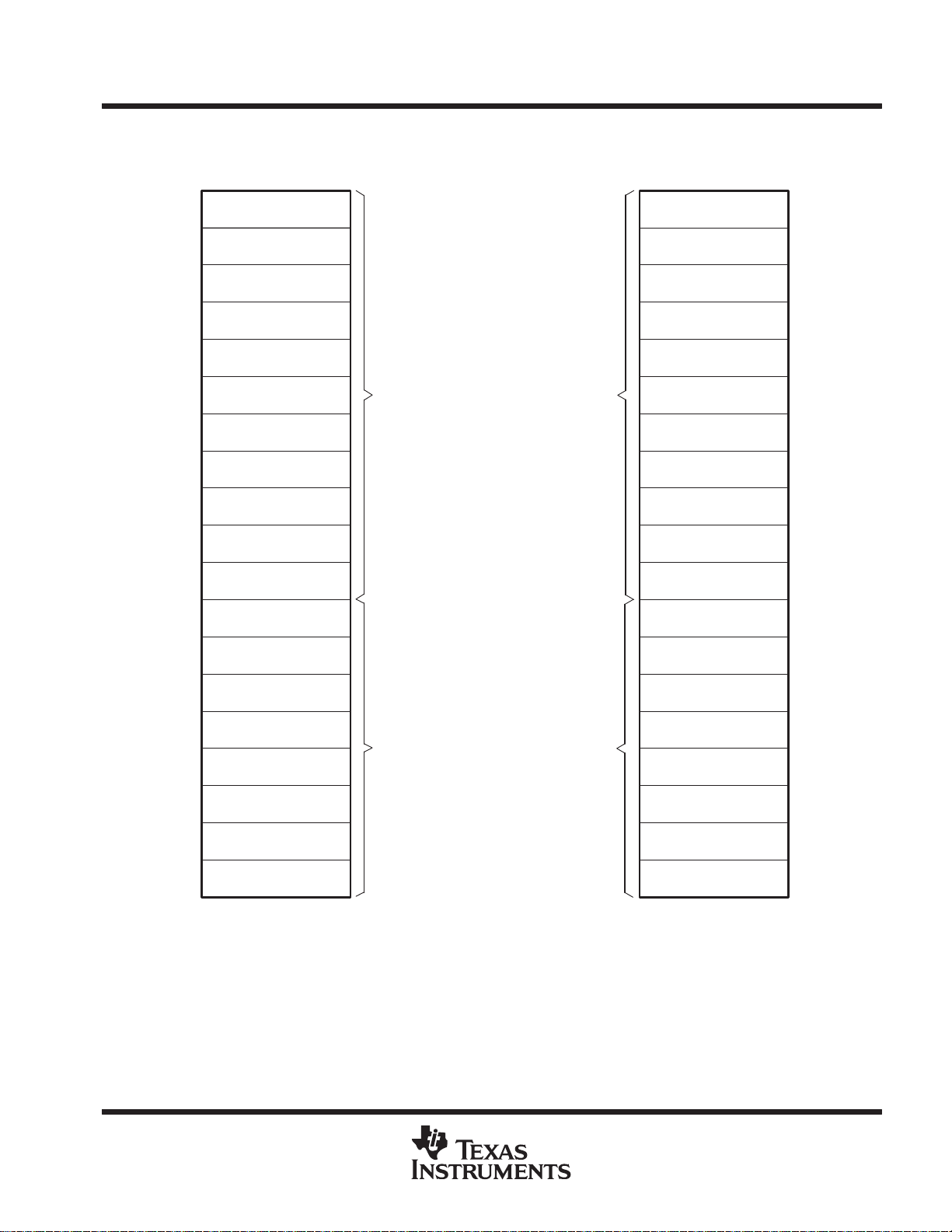
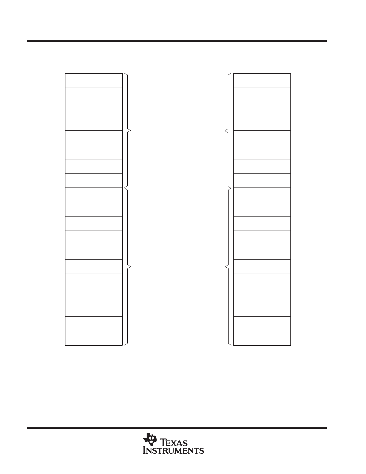
The TMS28F1600 is available with the sector architecture mapped with the boot block located at the top
(TMS28F1600T) or at the bottom (TMS28F1600B) of the memory array, as required by different
microprocessors. The bottom boot block is mapped with the 16K-byte boot block located at the low-order
address range (00000h to 01FFFh, word mode). The top boot block is mapped with the 16K-byte boot block
located at the high-order address range (FFFFFh to FE000h, word mode). Figure 1 and Figure 2 show the
memory maps for the top and bottom boot block configuration, respectively.
boot-sector data protection
The 16K-byte boot block can be used to store key system data that is seldom changed in normal operation. Data
in this block can be protected by using different combinations of the reset/power-down pin (RP
pin (WP
) and VPP supply levels. See Table 2 for a listing of these combinations.
DATA PROTECTION PROVIDED V
All sectors locked
All sectors locked (reset) X V
Only boot block locked
PRODUCT PREVIEW
Table 2. Data Protection Combinations
PP
V
PPLK
V
PPLK
V
PPLK
V
PPLK
RP WP
X X
IL
V
HH
V
IH
V
IH
), the write protect
X
X
V
IH
V
IL
4
POST OFFICE BOX 1443 • HOUSTON, TEXAS 77251–1443
Page 5
TMS28F1600T, TMS28F1600B
16M-BIT (1M BY 16, 2M BY 8)
CONCURRENT OPERATIONS AUTO-SELECT BOOT-BLOCK FLASH MEMORY
RP
OE
WE
CE
SMJS836 – JANUARY 1997
WRITE
STATE
PP
V
Erase
Program/
Byte
128K-
Byte
128K-
Byte
128K-
Byte
128K-
Byte
128K-
Byte
128K-
Byte
128K-
96K-
Byte
8K-
Byte
8K-
Byte
A
MACHINE
Voltge
Switch
Main
Main
Main
Main
Main
Main
Main
Main
Para
Para
BYTE
I/O
DATA
Y Gating/Senting
COMPARATOR
LOGIC
A
STATE
MACHINE
COMMAND
INPUT
BUFFER
INPUT
BUFFER
OUTPUTOUTPUT
BUFFER BUFFER
Data
Register A
ID REGISTER
STATUS REGISTER B
STATUS REGISTER A
OUTPUT MULTIPLEXER
DATA
COMPARATOR
B
STATE
MACHINE
COMMAND
Data
Register B
STATE
WRITE
MACHINE B
Erase
Switch
Voltage
Program/
Main
Byte
128K-
Main
Byte
128K-
Byte
Main
128K-128K-
Byte
Main
128K-128K-
Byte
Byte
128K-
Byte
128K-
Main
Main
Main
Y Gating/Sensing
PP
V
PRODUCT PREVIEW
16K-
Byte
ADDRESS
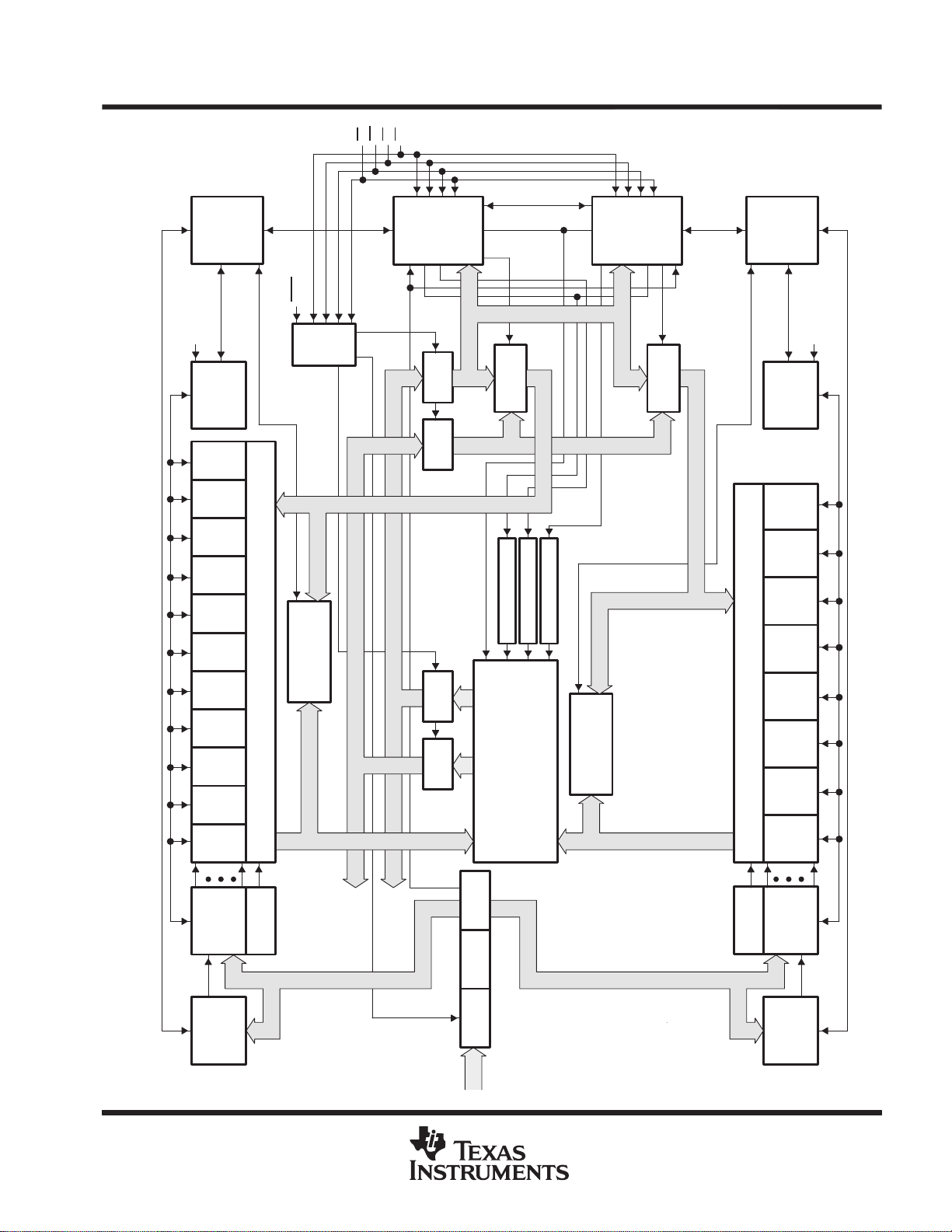
functional block diagram
Boot
Block
Y DECODER
X DECODER
A
COUNTER
DQ0–DQ7
DQ8–DQ15/A–1
POST OFFICE BOX 1443 HOUSTON, TEXAS 77251–1443
ADDRESS
LATCH DECODER
ADDRESS
INPUT
BUFFER
A0–A19
• 5
Byte
X DECODER
Y DECODER
COUNTER
ADDRESS
Main
B
Page 6

TMS28F1600T, TMS28F1600B
16M-BIT (1M BY 16, 2M BY 8)
CONCURRENT OPERATIONS AUTO-SELECT BOOT-BLOCK FLASH MEMORY
SMJS836 – JANUARY 1997
parameter sector
Two parameter sectors of 8K bytes each can be used like a scratch pad to store frequently updated data.
Alternatively , the parameter sectors can be used for additional boot or main-sector data. If a parameter sector
is used to store additional boot-block data, caution should be exercised because the parameter sector does not
have the boot-block data protection safety feature.
main sector
Primary memory on the TMS28F1600T/B is located in sixteen main sectors. Fifteen of the sectors have storage
capacity for 128K-bytes and the remaining sector has storage capacity of 96K bytes.
PRODUCT PREVIEW
6
POST OFFICE BOX 1443 • HOUSTON, TEXAS 77251–1443
Page 7
CONCURRENT OPERATIONS AUTO-SELECT BOOT-BLOCK FLASH MEMORY
main sector (continued)
TMS28F1600T, TMS28F1600B
16M-BIT (1M BY 16, 2M BY 8)
SMJS836 – JANUARY 1997
Address
Range
1FFFFFh
1FC000h
1FBFFFh
1FA000h
1F9FFFh
1F8000h
1F7FFFh
1E0000h
1DFFFFh
1C0000h
1BFFFFh
1A0000h
19FFFFh
180000h
17FFFFh
160000h
15FFFFh
140000h
13FFFFh
120000h
11FFFFh
100000h
FFFFFh
E0000h
DFFFFh
C0000h
BFFFFh
A0000h
9FFFFh
80000h
7FFFFh
60000h
5FFFFh
40000h
3FFFFh
20000h
1FFFFh
00000h
x8 Configuration x16 Configuration
Boot Sector
16K Address
Parameter Sector
8K Address
Parameter Sector
8K Address
Main Sector
96K Address
Main Sector
128K Address
Main Sector
128K Address
Main Sector
128K Address
Main Sector
128K Address
Main Sector
128K Address
Main Sector
128K Address
Main Sector
128K Address
Main Sector
128K Address
Main Sector
128K Address
Main Sector
128K Address
Main Sector
128K Address
Main Sector
128K Address
Main Sector
128K Address
Main Sector
128K Address
Main Sector
128K Address
Bank A
(Write State Machine A)(Write State Machine B)
Bank B
Bank A
(Write State Machine A)(Write State Machine B)
Bank B
Boot Sector
8K Address
Parameter Sector
4K Address
Parameter Sector
4K Address
Main Sector
48K Address
Main Sector
64K Address
Main Sector
64K Address
Main Sector
64K Address
Main Sector
64K Address
Main Sector
64K Address
Main Sector
64K Address
Main Sector
64K Address
Main Sector
64K Address
Main Sector
64K Address
Main Sector
64K Address
Main Sector
64K Address
Main Sector
64K Address
Main Sector
64K Address
Main Sector
64K Address
Main Sector
64K Address
Address
Range
FFFFFh
FE000h
FDFFFh
FD000h
FCFFFh
FC000h
FBFFFh
F0000h
EFFFFh
E0000h
DFFFFh
D0000h
CFFFFh
C0000h
BFFFFh
B0000h
AFFFFh
A0000h
9FFFFh
90000h
8FFFFh
80000h
7FFFFh
70000h
6FFFFh
60000h
5FFFFh
50000h
4FFFFh
40000h
3FFFFh
30000h
2FFFFh
20000h
1FFFFh
10000h
FFFFh
0000h
PRODUCT PREVIEW
Figure 1. TMS28F1600T (Top Boot Sector) Memory Map
POST OFFICE BOX 1443 • HOUSTON, TEXAS 77251–1443
7
Page 8
TMS28F1600T, TMS28F1600B
16M-BIT (1M BY 16, 2M BY 8)
CONCURRENT OPERATIONS AUTO-SELECT BOOT-BLOCK FLASH MEMORY
SMJS836 – JANUARY 1997
main sector (continued)
Address
Range
1FFFFFh
1E0000h
1DFFFFh
1C0000h
1BFFFFh
1A0000h
19FFFFh
180000h
17FFFFh
160000h
15FFFFh
140000h
13FFFFh
120000h
11FFFFh
100000h
FFFFFh
E0000h
DFFFFh
C0000h
BFFFFh
A0000h
9FFFFh
80000h
7FFFFh
60000h
5FFFFh
40000h
3FFFFh
PRODUCT PREVIEW
20000h
1FFFFh
8000h
7FFFh
6000h
5FFFh
4000h
3FFFh
00000h
x8 Configuration x16 Configuration
Main Sector
128K Address
Main Sector
128K Address
Main Sector
128K Address
Main Sector
128K Address
Main Sector
128K Address
Main Sector
128K Address
Main Sector
128K Address
Main Sector
128K Address
Main Sector
128K Address
Main Sector
128K Address
Main Sector
128K Address
Main Sector
128K Address
Main Sector
128K Address
Main Sector
128K Address
Main Sector
128K Address
Main Sector
96K Address
Parameter Sector
8K Address
Parameter Sector
8K Address
Boot Sector
16K Address
Bank B
Bank A
(Write State Machine A) (Write State Machine B)
Main Sector
64K Address
Main Sector
64K Address
Main Sector
64K Address
Main Sector
64K Address
Bank B
Bank A
(Write State Machine A) (Write State Machine B)
Main Sector
64K Address
Main Sector
64K Address
Main Sector
64K Address
Main Sector
64K Address
Main Sector
64K Address
Main Sector
64K Address
Main Sector
64K Address
Main Sector
64K Address
Main Sector
64K Address
Main Sector
64K Address
Main Sector
64K Address
Main Sector
48K Address
Parameter Sector
4K Address
Parameter Sector
4K Address
Boot Sector
8K Address
Address
Range
FFFFFh
FC000h
EFFFFh
E0000h
DFFFFh
D0000h
CFFFFh
C0000h
BFFFFh
B0000h
AFFFFh
A0000h
9FFFFh
90000h
8FFFFh
80000h
7FFFFh
70000h
6FFFFh
60000h
5FFFFh
50000h
4FFFFh
40000h
3FFFFh
30000h
2FFFFh
20000h
1FFFFh
10000h
FFFFh
4000h
3FFFh
3000h
2FFFh
2000h
1FFFh
00000h
Figure 2. TMS28F1600B (Bottom Boot Sector) Memory Map
8
POST OFFICE BOX 1443 • HOUSTON, TEXAS 77251–1443
Page 9
TMS28F1600T, TMS28F1600B
16M-BIT (1M BY 16, 2M BY 8)
CONCURRENT OPERATIONS AUTO-SELECT BOOT-BLOCK FLASH MEMORY
SMJS836 – JANUARY 1997
data protection
Data is secured or unsecured by using different combinations of the reset/power-down pin (RP), the write
protect pin (WP
) and VPP supply levels. Table 2 lists these combinations.
There are two ways to secure the entire memory against inadvertent alteration of data. The V
be held below the V
a logic-low level. Note that if RP
lock-out voltage level (V
PP
is held low, the device resets, which means it powers down and, therefore,
) or the reset/deep power-down pin (RP) can be pulled to
PPLK
supply pin can
PP
cannot be read. Typically, this pin is tied to the system reset for additional protection during system power up.
The boot sector has an additional security feature through the WP
the WP
is protected. When WP
pin controls whether the boot sector is protected. When WP is held at logic-low level, the boot sector
is held at logic-high level, the boot sector is unprotected along with the rest of the other
sectors. Alternatively, the entire memory can be unprotected by pulling the RP
pin. When the RP pin is at logic-high level,
pin to VHH (12 V).
command state machine (CSM)
There are two CSMs and each is corresponded to one WSM. The CSMs act as an interface between the external
microprocessor and the two internal WSMs. Commands are issued to the CSMs using standard microprocessor
write timings. Since both CSMs share the same data path, commands issued to the device are processed by
both CSMs simultaneously . If CSM A determines that the command is not applicable to the memory bank/WSM
that it is interfacing with (memory bank A), then that command is ignored and CSM B sends the command to
bank B/WSM B for execution. The CSM main task is to determine if the inputted command is valid and to send
the valid command to the corresponding WSM. In single-operation mode, the contents of both status registers
and the state of both CSMs are synchronized. Therefore, from the user’s point of view, the device behaves as
if there is only one CSM, one status register and one WSM that control both memory banks. In
concurrent-operations mode, the contents of both status registers and the state of both CSMs are independent.
When a program or erase command is issued to the CSM for one memory bank, the WSM for that memory bank
controls the internal program/erase sequences and the CSM responds to status-read and suspend/resume
only. After the WSM completes its task, the WSM status bit (SB7) is set to a logic-high level (1), allowing the
CSM to respond to the full command set again (see Table 5 for the status register bit definition). The complete
command sets are listed in Table 3 and the description of these commands are shown in Table 4.
Table 3. Command State Machine Codes for Device-Mode Selection
COMMAND CODE
ON DQ0–DQ7
00h Invalid / Reserved
10h Alternate Program Setup
20h Block-Erase Setup
40h Program Setup
50h Clear Status Register
70h Read Status Register
90h Algorithm Selection
B0h Erase-Program Suspend
D0h Erase-Program Resume / Block-Erase Confirm
FFh Read Array
CBh Enable Concurrent Mode
CEh Disable Concurrent Mode
†
DQ0 is the least significant bit. DQ8–DQ15 can be any valid 2-state level.
†
Standard Command Set
Extended Command Set
DEVICE MODE
PRODUCT PREVIEW
POST OFFICE BOX 1443 • HOUSTON, TEXAS 77251–1443
9
Page 10
TMS28F1600T, TMS28F1600B
BUS CYCLE
16M-BIT (1M BY 16, 2M BY 8)
CONCURRENT OPERATIONS AUTO-SELECT BOOT-BLOCK FLASH MEMORY
SMJS836 – JANUARY 1997
command state machine (CSM) (continued)
Table 4. Command Definitions for Single and Concurrent Operations
FIRST BUS CYCLE SECOND BUS CYCLE
COMMAND
Read Array 1 Write
Read Algorithm-Selection Code 3 Write X 90h Read A0 M/D
Read Status Register 2 Write X 70h Read
Clear Status Register 1 Write
Program-Setup / Program
(byte/word)
Program-Suspend/
Program-Resume
Block-Erase Setup/
Block-Erase Confirm
Erase-Suspend/
Erase-Resume
Enable Concurrent Mode
(see Note 2)
Disable Concurrent Mode
(see Note 2)
Legend:
PRODUCT PREVIEW
BEA Block-erase address. Any address selected within a block selects that block for erase.
M/D Manufacturer-equivalent / device-equivalent code
PA Address to be programmed
PD Data to be programmed at PA
RA Address to be read from
SRB Status-register data byte that can be found on DQ0–DQ7
X Don’t care
NOTES: 1. For single operation: address = don’t care
For concurrent operation:
address = 0xxxxxh for low-order address memory bank/WSM
address = 1xxxxxh for high-order address memory bank/WSM
2. To operate the device concurrently , the user must first issue the enable concurrent mode command. This command is valid only when
the device is not busy performing any operation (that is, WSM is not active). To exit the concurrent-operation mode, the user must
issue the disable concurrent mode command. This command is valid only when the device is in concurrent-operations mode and
none of the memory banks/WSMs are active.
REQUIRED
2 Write PA 40h or 10h Write PA PD
2 Write
2 Write BEA 20h Write BEA D0h
2 Write
1 Write X CBh
1 Write X CEh
OPERATION ADDRESS
Read Operations
See Notes
1 and 2
See
Notes 1
and 2
Program Operations
See
Notes 1
and 2
Erase Operations
See
Notes 1
and 2
Concurrent Operations
DATA
INPUT
FFh Read RA Data Out
50h
B0h Write
B0h Write
OPERATION ADDRESS
See
Note 1
See
Note 1
See
Notes 1
and 2
DATA
IN/OUT
SRB
D0h
D0h
10
POST OFFICE BOX 1443 • HOUSTON, TEXAS 77251–1443
Page 11

TMS28F1600T, TMS28F1600B
16M-BIT (1M BY 16, 2M BY 8)
CONCURRENT OPERATIONS AUTO-SELECT BOOT-BLOCK FLASH MEMORY
SMJS836 – JANUARY 1997
operation
The TMS28F1600T/B is capable of performing either single or concurrent operations. Single operation means
that the device is performing one operation on one memory bank at a time, or in other words, only one WSM
is active. A WSM is considered active even when it is in a suspended state. Therefore, from the user’s point
of view, the device behaves as if there is only one WSM that controls both memory banks. Concurrent operations
mean that the device is performing two operations on two memory banks simultaneously , or in other words, both
WSMs are active.
Device operations are selected by entering 8-bit command codes with conventional microprocessor timing into
two on-chip CSMs through I/O pins DQ0–DQ7. When the device is powered up, internal reset circuitry initializes
the CSMs to single-operation, read-array mode. In single-operation mode, the device is functionally compatible
with the existing 8-Mbit boot-block devices (TMS28F800T/B). Changing the mode of operation requires a
command code to be entered into the CSM. Table 3 lists the CSM codes for all modes of operation.
To enable the concurrent-operations mode, the user must issue the enable concurrent mode command to the
CSM. This command is valid only when the device is not busy performing any operation (that is, WSM is not
active). Once the concurrent-operations mode is enabled, both status registers are cleared, both CSMs are
reset to the read-array mode, and any commands issued to the CSMs from that point forward must be in
accordance with the concurrent-operations command definitions. Command definitions for both single and
concurrent-operations modes are listed in Table 4. Note that both command definitions are the same except
for four commands: read array, read status register, clear status register, and suspend/resume. In
single-operation mode, the addresses are don’t care for those commands. However, in concurrent-operations
mode, the user must indicate to the CSMs to which write-state machine/memory bank the command is
applicable by supplying the memory bank address. This is the only difference between single and concurrent
operations as far as command definitions are concerned.
To initiate concurrent operations once the concurrent mode is enabled, the user sequentially issues two
commands to the CSMs, one for each memory bank; the issued commands must be in accordance with the
concurrent-operations command definitions. Note that while the concurrent mode is enabled, the user does not
have to operate the device concurrently; the user can operate the device as in single-operation mode but with
the command definitions slightly modified. In addition, the user can access and clear each status register
individually in concurrent mode.
To exit the concurrent-operations mode and return to the standard flash single-operation mode, the user must
issue a disable concurrent mode command to the CSMs. This command is valid only when the device is in
concurrent-operations mode and none of the memory banks/WSMs are active. Once concurrent-operations
mode is disabled, both status registers are cleared and both CSMs reset to the read-array mode. Alternatively ,
the user can use the reset/power-down mode to reset the device to single-operation, read-array mode.
Since both registers are cleared when concurrent-operations mode is enabled/disabled, it is recommended that
the status register be read, if required, before the concurrent mode is enabled/disabled.
concurrent operations
Since the TMS28F1600T /B has two independent WSMs, two operations can be performed on two memory
banks concurrently. However, there are some rules and restrictions that must be adhered to when operating
the device concurrently.
First, read is an operation that cannot be performed concurrently with another read. Second, if read is to be a
part of a concurrent operation, then read must be the last command issued to the CSM. Third, once a read
command is issued, the CSM does not accept
array , read algorithm-selection, read status register and clear status register commands are considered to be
the same (that is, a read operation) as far as concurrent operations are concerned.
any other command
until the read operation is complete. Read
PRODUCT PREVIEW
POST OFFICE BOX 1443 • HOUSTON, TEXAS 77251–1443
11
Page 12

TMS28F1600T, TMS28F1600B
16M-BIT (1M BY 16, 2M BY 8)
CONCURRENT OPERATIONS AUTO-SELECT BOOT-BLOCK FLASH MEMORY
SMJS836 – JANUARY 1997
concurrent operations (continued)
For example, a concurrent read-erase operation is
command, no other command is processed until the read operation is complete. Whereas, a concurrent
erase-read operation is possible because the erase command is given first (for example, to erase a sector in
memory bank A) and the read command is given last (for example, to access bank B). Only when the read
operation is complete, is the CSM ready to accept any other valid command. At this point, the user has two
options from which to choose. If operation on memory bank B is desired, then the user can send a read, program,
or erase command. If operation on memory bank A is desired, then the user can either do an erase-suspend
to read or an erase-suspend to program; both of which must be done in a sector that is not being erased.
Two rules/restrictions govern the suspend operation:
D
Read array, read status register, and program-resume are the only valid commands for the applicable
WSM / memory bank after a program operation is suspended; all other commands are invalid and are
ignored by the CSM. If concurrent-operations mode is enabled, then the other CSM will accept any other
valid command for the other WSM/memory bank.
D
Read array , read status register, program, and erase-resume are the only valid commands for the applicable
WSM/memory bank after a sector-erase operation is suspended; all other commands are invalid and are
ignored by the CSM. If concurrent-operations mode is enabled, then the other CSM will accept any other
valid command for the other WSM/memory bank.
In general, any operation or combination of operations is possible as long as it does not violate the
rules/restrictions mentioned above. Note that multiple suspension within the same memory bank is allowed.
For example, if an erase operation is suspended for a program operation, then that program operation can also
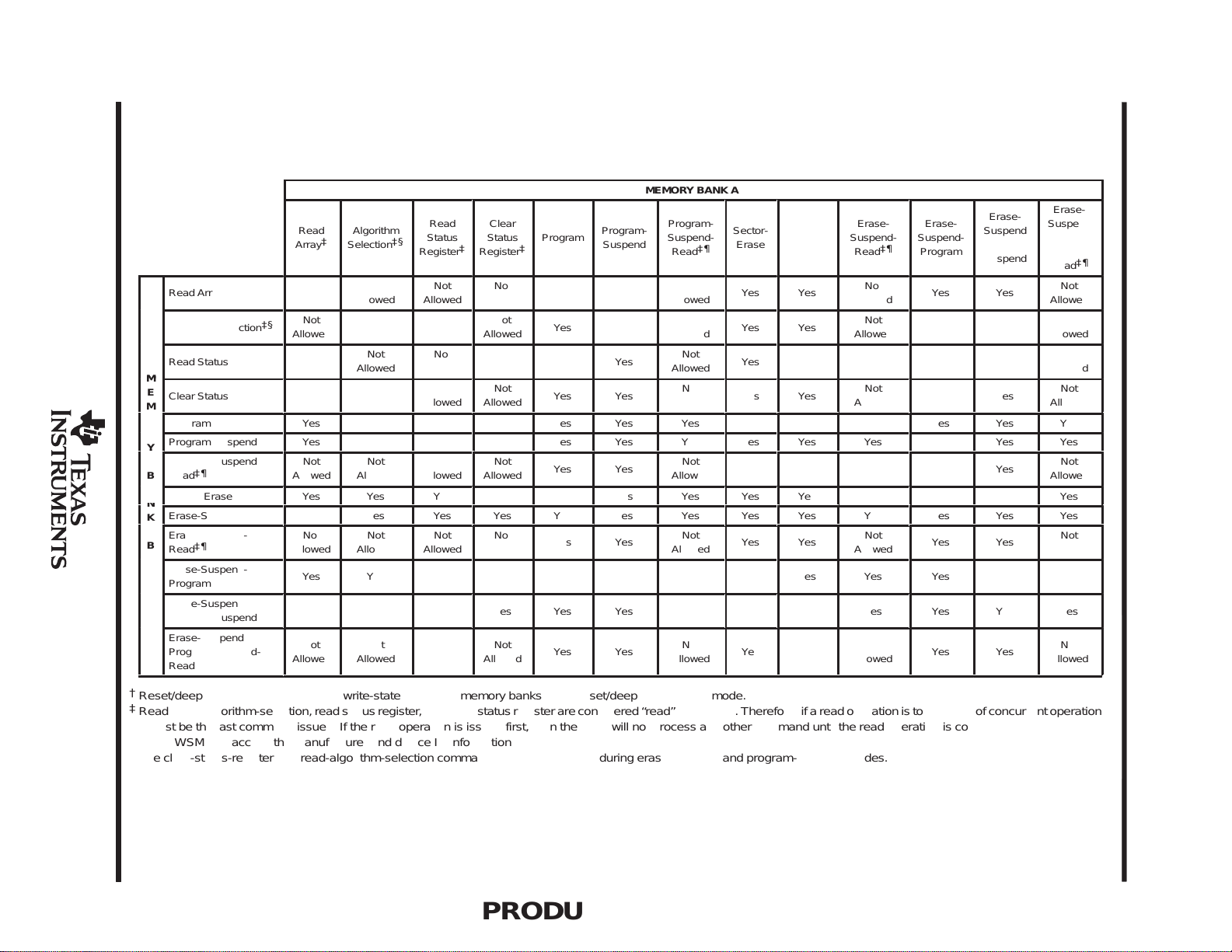
be suspended to read data. Table 5 shows all the legal operations that can be performed concurrently.
not
possible because as soon as the CSM receives the read
PRODUCT PREVIEW
12
POST OFFICE BOX 1443 • HOUSTON, TEXAS 77251–1443
Page 13
concurrent operations (continued)
Á
Á
Á
Á
Á
Á
Á
Á
Á
Á
Á
Á
Á
Á
Á
Á
Á
Á
Á
Á
Á
Á
Á
Á
Á
Á
Á
Á
Á
Á
Á
Á
Á
Á
Á
Á
Á
Á
Á
Á
Á
Á
M
Á
Á
Á
Á
Á
Á
Á
Á
Á
Á
Á
Á
Á
Á
R
Y
Á
Á
Á
Á
Á
Á
Á
Á
Á
Á
Á
Á
Á
Á
N
Á
Á
Á
Á
Á
Á
Á
Á
Á
Á
Á
Á
Á
Á
Á
Á
Á
Á
Á
Á
Á
Á
Á
Á
Á
Á
Á
Á
Á
Á
Á
Á
Á
Á
Á
Á
Á
Á
Á
Á
Á
Á
POST OFFICE BOX 1443 HOUSTON, TEXAS 77251–1443
• 13
ÁÁÁÁ
ÁÁÁÁ
Read Array
Algorithm Selection
ÁÁÁÁ
Read Status Register
E
Clear Status Register
ÁÁÁÁ
M
O
Program
Program-Suspend
Y
Program-Suspend-
‡¶
ÁÁÁÁ
Read
B
A
Sector-Erase
Erase-Suspend
K
Erase-Suspend-
B
ÁÁÁÁ
‡¶
Read
Erase-Suspend-
Program
Erase-Suspend
ÁÁÁÁ
Program-Suspend
Erase-Suspend
Program-Suspend-
‡¶
ÁÁÁÁ
Read
Table 5. Concurrent Operations State Matrix
†
MEMORY BANK A
Erase-
Suspend
ÁÁ
Program-
Suspend
ÁÁ
Yes
Yes
ÁÁ
Yes
Yes
ÁÁ
Yes
Yes
Yes
ÁÁ
Yes
Yes
Yes
ÁÁ
Yes
Yes
ÁÁ
Yes
ÁÁ
Read
ÁÁ
Array
ÁÁ
‡§
Allowed
ÁÁ
Allowed
‡
Allowed
‡
ÁÁ
Allowed
Not
Not
Not
Not
‡
Yes
Yes
Not
ÁÁ
Allowed
Yes
Yes
Not
ÁÁ
Allowed
Yes
Yes
ÁÁ
Not
Allowed
ÁÁ
‡
Algorithm
ÁÁ
Selection
ÁÁ
Not
Allowed
Not
ÁÁ
Allowed
Not
Allowed
Not
ÁÁ
Allowed
Yes
Yes
Not
ÁÁ
Allowed
Yes
Yes
Not
ÁÁ
Allowed
Yes
Yes
ÁÁ
Not
Allowed
ÁÁ
‡§
Read
Á
Status
Register
Á
Not
Allowed
Not
Á
Allowed
Not
Allowed
Not
Á
Allowed
Yes
Yes
Not
Á
Allowed
Yes
Yes
Not
Á
Allowed
Yes
Yes
Á
Not
Allowed
Á
‡
Clear
ÁÁ
Status
Register
ÁÁ
Not
Allowed
Not
ÁÁ
Allowed
Not
Allowed
Not
ÁÁ
Allowed
Yes
Yes
Not
ÁÁ
Allowed
Yes
Yes
Not
ÁÁ
Allowed
Yes
Yes
ÁÁ
Not
Allowed
ÁÁ
‡
Á
Program
Á
Yes
Yes
Á
Yes
Yes
Á
Yes
Yes
Yes
Á
Yes
Yes
Yes
Á
Yes
Yes
Á
Yes
Á
Program-
ÁÁ
Suspend
ÁÁ
Yes
Yes
ÁÁ
Yes
Yes
ÁÁ
Yes
Yes
Yes
ÁÁ
Yes
Yes
Yes
ÁÁ
Yes
Yes
ÁÁ
Yes
ÁÁ
Program-
ÁÁ
Suspend-
‡¶
Read
ÁÁ
Not
Allowed
Not
ÁÁ
Allowed
Not
Allowed
Not
ÁÁ
Allowed
Yes
Yes
Not
ÁÁ
Allowed
Yes
Yes
Not
ÁÁ
Allowed
Yes
Yes
ÁÁ
Not
Allowed
ÁÁ
Sector-
Á
Erase
Á
Yes
Yes
Á
Yes
Yes
Á
Yes
Yes
Yes
Á
Yes
Yes
Yes
Á
Yes
Yes
Á
Yes
Á
Erase-
ÁÁ
Suspend
ÁÁ
Yes
Yes
ÁÁ
Yes
Yes
ÁÁ
Yes
Yes
Yes
ÁÁ
Yes
Yes
Yes
ÁÁ
Yes
Yes
ÁÁ
Yes
ÁÁ
Erase-
ÁÁ
Suspend-
‡¶
Read
ÁÁ
Not
Allowed
Not
ÁÁ
Allowed
Not
Allowed
Not
ÁÁ
Allowed
Yes
Yes
Not
ÁÁ
Allowed
Yes
Yes
Not
ÁÁ
Allowed
Yes
Yes
ÁÁ
Not
Allowed
ÁÁ
Erase-
Á
Suspend-
Program
Á
Yes
Yes
Á
Yes
Yes
Á
Yes
Yes
Yes
Á
Yes
Yes
Yes
Á
Yes
Yes
Á
Yes
Á
Erase-
Suspend
ÁÁ
ProgramSuspend-
ÁÁ
‡¶
Read
Not
Allowed
Not
ÁÁ
Allowed
Not
Allowed
Not
ÁÁ
Allowed
Yes
Yes
Not
ÁÁ
Allowed
Yes
Yes
Not
ÁÁ
Allowed
Yes
Yes
ÁÁ
Not
Allowed
ÁÁ
CONCURRENT OPERATIONS AUTO-SELECT BOOT-BLOCK FLASH MEMORY
TMS28F1600T, TMS28F1600B
16M-BIT (1M BY 16, 2M BY 8)
†
Reset/deep power-down places both write-state machines/memory banks in the reset/deep power-down mode.
‡
Read array, algorithm-selection, read status register, and clear status register are considered “read” operations. Therefore, if a read operation is to be a part of concurrent operations,
it must be the last command issued. If the read operation is issued first, then the CSM will not process any other command until the read operation is complete.
§
Either WSM can access the manufacturer and device ID information
¶
The clear-status-register and read-algorithm-selection commands are not functional during erase-suspend and program-suspend modes.
PRODUCT PREVIEW
SMJS836 – JANUARY 1997
Page 14

TMS28F1600T, TMS28F1600B
16M-BIT (1M BY 16, 2M BY 8)
CONCURRENT OPERATIONS AUTO-SELECT BOOT-BLOCK FLASH MEMORY
SMJS836 – JANUARY 1997
command definition
Command definitions for both single and concurrent operations are listed in Table 4. Note that both command
definitions are the same except for four commands: read array, read status register, clear status register, and
suspend / resume. In single-operation mode, the address is a don’t care for these commands. However, in
concurrent-operations mode, the user must indicate to the CSM which write-state machine/memory bank the
command is applicable to by supplying the memory bank address.
In single-operation mode, the user can use either single or concurrent operations command definitions to send
the desired command to the CSM. However, once the concurrent-operations mode is enabled, all subsequent
commands issued must be in accordance with the concurrent-operations mode command definitions.
Once a specific command code has been entered, the WSM executes an internal algorithm generating the
necessary timing signals to program, erase, and verify data. See Table 4 for the CSM command definitions and
data for each of the bus cycles.
Following the read-algorithm-selection-code command, two read cycles are required to access the
manufacturer-equivalent code and the device-equivalent code. Table 7 and Table 8 show the code for
word-wide mode and byte-wide mode, respectively.
status register
There are two 8-bit on-chip status registers. Status register A corresponds to WSM A and status register B
corresponds to WSM B. The status register can be monitored to see whether the state of a program/erase
operation is pending or complete by writing a read-status command to the CSM and reading the resulting status
code on I/O pins DQ0–DQ7. This is valid for operation in either the byte or word-wide mode. When writing to
the CSM in word-wide mode, the high-order I/O pins (DQ8–DQ15) can be set to any valid 2-state level. When
reading the status bit during a word-wide read operation, the high-order I / Os (DQ8–DQ15) are set to 00h
internally, so the user needs to interpret only the low-order I/O pins (DQ0–DQ7).
After a read-status command has been given, the data appearing on DQ0–DQ7 remains as status register data
until a new command is issued to the CSM. To return the device to other modes of operation, a new command
must be issued to the CSM.
Register data is updated on the falling edge of OE
updates the latches within a given read cycle. Latching the data prevents errors from occurring should the
PRODUCT PREVIEW
register input change during a status register read. To assure that the status register output contains updated
status data, CE
The status registers provide the internal state of the WSMs to the external microprocessor. During periods when
the WSMs are active, the status registers can be polled to determine the status of the WSMs. Table 6 defines
the status register bits and their functions.
In single-operation mode, the contents of both status registers and the state of both CSMs are synchronized.
Therefore, from the user’s point of view, the device behaves as if only one CSM, one status register, and one
WSM are controlling both memory banks. In concurrent-operations mode, the contents of both status registers
and the state of both CSMs are independent. Therefore, in concurrent-operations mode, the user can access
and clear each status register individually.
or OE must be toggled for each subsequent status read.
or CE. The latest falling edge of either of these two signals
14
POST OFFICE BOX 1443 • HOUSTON, TEXAS 77251–1443
Page 15

CONCURRENT OPERATIONS AUTO-SELECT BOOT-BLOCK FLASH MEMORY
status register (continued)
Table 6. Status-Register Bit Definitions and Functions (see Note 3)
TMS28F1600T, TMS28F1600B
16M-BIT (1M BY 16, 2M BY 8)
SMJS836 – JANUARY 1997
STATUS
BIT
SB7
SB6
SB5
SB4
SB3
SB2
SB0–SB1 Reserved These bits must be masked out when reading the status register.
NOTE 3: V
PPL
FUNCTION DATA COMMENTS
Write state machine
status
Erase-suspend status
(ESS)
Erase status
(ES)
Program status
(PS)
Vpp status
(Vpps)
Program-suspend
status (PSS)
and V
correspond to the minimum and maximum operating voltage range of VPP, respectively.
PPH
1 = Ready
0 = Busy
1 = Erase suspended
0 = Erase in progress or
completed
1 = Sector-erase error
0 = Sector-erase good
1 = Byte/word program error
0 = Byte/word program good
1 = Program abort :
Vpp range error
0 = Vpp good
1 = Program suspended
0 = Program in progress or
completed
If SB7 = 0 (busy), the WSM has not completed an erase or
programming operation. If SB7 = 1 (ready), other polling operations can
be performed. Until this occurs, the other status bits are not valid. If the
WSM status bit shows busy (0), the user must periodically toggle CE
or OE to determine when the WSM has completed an operation
(SB7 = 1) since SB7 is not updated automatically at the completion of
a WSM task.
When an erase-suspend command is issued, the WSM halts execution
and sets the ESS bit high (SB6 = 1), indicating that the erase operation
has been suspended. The WSM status bit also is set high (SB 7 =1)
indicating that the erase-suspend operation has been completed
successfully. The ESS bit remains at a logic-high level until an
erase-resume command is input to the CSM (code D0h).
SB5 = 0 indicates that a successful sector erasure has occurred.
SB5 = 1 indicates that an erasure error has occurred. In this case, the
WSM has completed the maximum allowed erase pulses determined
by the internal algorithm, but this was insufficient to erase the device
completely.
SB4 = 0 indicates successful programming has occurred at the
addressed sector location.
SB4 = 1 indicates that the WSM was unable to program the addressed
sector location correctly.
SB3 provides information on the status of Vpp during programming. If
Vpp is lower than V
issued, SB3 is set to a 1, indicating that the programming operation is
aborted. If Vpp is between V
When a program-suspend command is issued, the WSM halts
execution and sets the PSS bit high (SB2 = 1), indicating that the
program operation has been suspended. The WSM status bit also is set
high (SB 7 =1) indicating that the program-suspend operation has been
completed successfully. The PSS bit remains at a logic-high level until
a program-resume command is input to the CSM (code D0h).
after a program or erase command has been
PPL
PPH
and V
, SB3 is not set.
PPL
PRODUCT PREVIEW
byte- or word-wide mode selection
Device operation is either byte-wide or word-wide mode user-selectable and is determined by the logic state
of BYTE
from, I/O pins DQ0–DQ15. When BYTE
written to, or read from, I/O pins DQ0–DQ7. In the byte-wide mode, I/O pins DQ8–DQ14 are placed in the
high-impedance state and DQ15/A-1 becomes the low-order address pin. Table 7 and Table 8 summarize
operations for word-wide mode and byte-wide mode, respectively.
. When BYTE is at logic-high level, the device is in the word-wide mode and data is written to, or read
is at logic-low level, the device is in the byte-wide mode and data is
POST OFFICE BOX 1443 • HOUSTON, TEXAS 77251–1443
15
Page 16

TMS28F1600T, TMS28F1600B
X
VILVILVIHVIHVIDVIHX
X
VILVILVIHVIHVIDVIHXXHi-Z
16M-BIT (1M BY 16, 2M BY 8)
CONCURRENT OPERATIONS AUTO-SELECT BOOT-BLOCK FLASH MEMORY
SMJS836 – JANUARY 1997
byte- or word-wide mode selection (continued)
Table 7. Operation Modes for Word-Wide Mode (BYTE = VIH) (see Note 4)
MODE WP CE OE RP WE A9 A0 V
Read X V
X V
Algorithm-selection mode
Output disable X V
Standby X V
Reset/deep power down X X X V
V
IL
Write (see Notes 3 and 5)
or
V
IH
IL
IL
IL
IH
V
IL
Table 8. Operation Modes for Byte-Wide Mode (BYTE = VIL) (see Note 4)
MODE WP CE OE RP WE A9 A0 VPP
Read lower byte X V
Read upper byte X V
X V
Algorithm-selection mode
Output disable X V
Standby X V
Reset/deep power down X X X V
PRODUCT PREVIEW
Write (see Notes 3 and 5)
NOTES: 3. V
4. X = don’t care
5. When writing commands to the ’28F1600T/B, VPP must be in the appropriate VPP voltage range for sector-erase or program
and V
PPL
commands to be executed. Also, depending on the combination of RP
programmable (see Table 2 for the combinations).
V
IL
or
V
IH
correspond to the minimum and maximum operating voltage range of VPP, respectively.
PPH
V
IL
ILVIHVIH
V
IL
ILVIHVIH
V
IL
ILVIHVIHVIDVIL
ILVIHVIHVIH
X V
IH
V
ILVIH
V
IL
V
IL
V
IH
X V
V
IH
IH
IL
V
IH
or
V
HH
PP
V
V
IH
V
V
IH
V
V
IH
IH
IL
V
IH
or
V
HH
A9 A0 X V
A9 A0 X V
X X X X Hi-Z Hi-Z
X X X X X Hi-Z Hi-Z
X X X X X Hi-Z Hi-Z
V
A9 A0
IL
A9 A0 X Data out
IH
IHVID
IH
X X X X Hi-Z
X X X X Hi-Z
V
IL
V
X X X Hi-Z
A9 A0
X X Hi-Z Manufacturer-equivalent
V
PPL
or
V
PPH
and WP , the boot block can be secured and, therefore, is not
X Manufacturer-equivalent code 0089h
IL
Device-equivalent code 00xxh
(top boot block)
Device-equivalent code 00xxh
(bottom boot block)
V
PPL
or
V
DQ15/
A–1
Data in
PPH
DQ14–DQ8 DQ7–DQ0
IL
IH
X Hi-Z Data in
Hi-Z Data out
Hi-Z Data out
code 89h
Device-equivalent code
??h (top boot block)
Device-equivalent code
??h (bottom boot block)
DQ15–DQ0
command state machine (CSM) operations
The CSM decodes instructions for read, read algorithm-selection code, read status register, clear status
register, program, erase, erase/program suspend, and erase/program resume. The 8-bit command code is
input to the device on DQ0–DQ7 (see Table 3 for CSM codes). The CSMs act as an interface between the
external microprocessor and the two internal WSMs. During a program/erase cycle, the CSM informs the
applicable WSM (based on the input address) that a program or erase has been requested. The selected WSM
controls the program/erase sequences during a program/erase cycle and the CSM responds only to status read
and program/erase suspend commands. If concurrent-operations mode is enabled, then the other CSM will
respond to the full command set (if idle) or any valid command (if busy) for the other bank.
16
POST OFFICE BOX 1443 • HOUSTON, TEXAS 77251–1443
Page 17

TMS28F1600T, TMS28F1600B
16M-BIT (1M BY 16, 2M BY 8)
CONCURRENT OPERATIONS AUTO-SELECT BOOT-BLOCK FLASH MEMORY
SMJS836 – JANUARY 1997
command state machine (CSM) operations (continued)
When the WSM has completed its task, the WSM status bit (SB7) of the status register is set to a logic-high level
and the CSM responds to the full command set again. In single-operation mode, the states of both CSMs are
synchronized and remain in the last issued command state until the microprocessor issues another command.
In concurrent-operations mode, the state of each CSM is independent and they also remain in the last issued
command state until the microprocessor issues another command.
The WSM successfully initiates an erase or program operation only when V
To prevent inadvertent program/erase to the device, it is recommended that RP
signal.
is within its correct voltage range.
PP
be tied to the system reset
clear status register
The internal circuitry can set only the VPP status (SB3), the program status (SB4), and the erase-status bit (SB5)
of the status register. The clear-status register command (50h) allows the external microprocessor to clear these
status bits and synchronize to internal operations. When the status bits are cleared, the CSM returns to the
read-array mode. This is true for both single and concurrent operations mode. In single-operation mode, the
clear-status-register command clears both status registers. In concurrent operations mode, the memory bank
address determines which register to clear (see Table 4 for concurrent operations command definitions). Note
that clear status register command is not functional during program-suspend and erase-suspend modes.
read operations
There are three read operations available: read array , read algorithm-selection code, and read status register .
D
Read array . The array is read by entering the command code FFh on DQ0–DQ7. Control pins CE and OE
must be at a logic-low level (VIL) and WE and RP must be at a logic-high level (VIH) to read data from the
memory bank. Data is available on DQ0–DQ15 (word-wide mode) or DQ0–DQ7 (byte-wide mode). Any
valid address within any of the sectors selects that sector and allows data to be read from the sector.
D
Read algorithm-selection code. Algorithm-selection codes are read by entering command code 90h on
DQ0–DQ7. Two bus cycles are required for this operation: the first to enter the command code and the next
two to read the manufacturer equivalent and the device-equivalent codes. Control pins CE
be at the logic-low level (V
accessed by toggling A0. The manufacturer-equivalent code is obtained on DQ0 – DQ7 with A0 at the
logic-low level (V
Alternately , the manufacturer- and device-equivalent codes can be read by applying V
to A9 and selecting the desired code by toggling A0 high or low. All other addresses are “don’t care” (see
Table 4, Table 7 and Table 8). Note that algorithm-selection operation can be done concurrently with the
program/erase operation since the information can be accessed by either WSM (see Table 5).
). The device-equivalent code is obtained when A0 is set to a logic-high level (VIH).
IL
) and WE and RP must be at the logic-high level (VIH). Two identifier bytes are
IL
and OE must
(nominally 12 V)
ID
PRODUCT PREVIEW
D
Read status register. The status register is read by entering the command code 70h on DQ0–DQ7. Control
pins CE
bus cycles are required for this operation: one to enter the command code and a second to read the status
register. In a given read cycle, status-register contents are updated on the falling edge of CE
whichever occurs last within the cycle. For concurrent operations, the user must specify which register to
read status from by supplying the memory bank address. For single operations, the address is a don’t care
(see Table 4).
and OE must be at a logic-low level (VIL) and WE and RP must be at a logic-high level (VIH). Two
POST OFFICE BOX 1443 • HOUSTON, TEXAS 77251–1443
or OE,
17
Page 18

TMS28F1600T, TMS28F1600B
16M-BIT (1M BY 16, 2M BY 8)
CONCURRENT OPERATIONS AUTO-SELECT BOOT-BLOCK FLASH MEMORY
SMJS836 – JANUARY 1997
programming operations
There are three CSM commands for programming: program setup, alternate program setup, and program
suspend/resume (see Table 4).
Program setup and alternate program setup are the same as far as the programming operation is concerned
except that they have different command codes.
D
Program setup. After the program setup command code is entered, the selected WSM takes over and
correctly sequences the device to complete the program operation. During this time, the CSM responds only
to status-read and -suspend commands (see Figure 3 and Figure 4). If the concurrent-operations mode is
enabled, then the other CSM will respond to the full command set or any valid command for the other bank.
T aking RP
in the appropriate V
combinations of RP
therefore, cannot be programmed (see T able 2 for a list of combinations). Only 0s are written and compared
during a program operation. If 1s are programmed, the memory-cell contents do not change and no error
occurs.
A program-setup command can be aborted by writting FFh (in byte-wide mode) or FFFFh (in word-wide
mode) during the second cycle. After writing all 1s during the second cycle, the CSM responds only to status
reads. When the WSM status bit (SB7) is set to a logic-high level, signifying that the nonprogram operation is
terminated, all commands for the applicable bank to the CSM become valid again.
D
Program suspend/program resume. During the execution of a programming operation, the
program-suspend command (B0h) can be entered to direct the WSM to suspend the programming
operation. Once the WSM has reached the suspend state, it allows the CSM to respond only to the
read-array, read-status register, and program-resume commands. While the selected WSM is in the
program-suspend state, data from any address location except for the location that was being programmed
can be read. To resume the programming operation, a program-resume command (D0h) must be issued
to make the CSM clear the suspend state that was set previously.
If concurrent-operations mode is enabled, then the user must specify which memory bank/WSM to
suspend/resume by supplying the memory bank address. Programming on the low-order address memory
bank is suspended/resumed if the address input is within its valid address range (that is, A19 = 0).
PRODUCT PREVIEW
Programming on the high-order address memory bank is suspended/resumed if the address input is within
its valid address range (that is, A19 = 1). While the selected memory bank/WSM is in the program-suspend
state, data from any address location
programmed) can be read. Figure 5 shows the program suspend/resume flowchart.
to VIL during programming aborts the program operation. During programming, VPP must remain
voltage range as shown in the recommended operating conditions table. Different
PP
, WP, and VPP pin voltage levels ensure that data in certain sectors are protected, and,
within the same memory bank
(except for the location that was being
18
POST OFFICE BOX 1443 • HOUSTON, TEXAS 77251–1443
Page 19

TMS28F1600T, TMS28F1600B
16M-BIT (1M BY 16, 2M BY 8)
CONCURRENT OPERATIONS AUTO-SELECT BOOT-BLOCK FLASH MEMORY
SMJS836 – JANUARY 1997
Start
Issue Program-Setup
Command and Byte Address
Issue Byte
Address/Data
Read Status-Register
Full Status-Register
Byte-Program Completed
FULL STATUS-REGISTER-CHECK FLOW
Status-Register Bits
Bits
SB7 = 1
?
Yes
Check (optional)
Read
No
No
Program
Suspend
?
See Note A
Program
Suspend
Loop
Yes
BUS
OPERATION
Write
Write
Read
Standby
Repeat for subsequent bytes.
Write FFh after the last byte-programming operation to reset
the device to read-array mode
COMMAND COMMENTS
Write
program
setup
Write data Data = Byte to be
Data = 40h or 10h
Addr = Address of byte to
Addr = Address of byte to
Status-register data.
Single-operation mode:
Addr = don’t care
Concurrent-operations mode:
Addr = 0xxxxxh for
Toggle OE
status register
Check SB7
1 = Ready, 0 = Busy
be programmed
programmed
be programmed
low-order address
memory bank
= 1xxxxxh for
high-order address
memory bank
or CE to update
SB3 = 0
?
Yes
SB4 = 0
?
Yes
Byte-Program Passed
NOTES: A. Full status-register check can be done after each byte or after a sequence of bytes.
B. SB3 must be cleared before attempting additional program/erase operations.
C. SB4 is cleared only by the clear-status-register command, but it does not prevent additional program operation attempts.
No
No
VPP Range Error
Byte-Program
Failed
BUS
OPERATION
Standby
Standby
Figure 3. Automated Byte-Programming Flowchart
COMMAND COMMENTS
Check SB3
1 = Detect VPP low
(see Note B)
Check SB4
1 = Byte-program error
(see Note C)
PRODUCT PREVIEW
POST OFFICE BOX 1443 • HOUSTON, TEXAS 77251–1443
19
Page 20

TMS28F1600T, TMS28F1600B
16M-BIT (1M BY 16, 2M BY 8)
CONCURRENT OPERATIONS AUTO-SELECT BOOT-BLOCK FLASH MEMORY
SMJS836 – JANUARY 1997
Start
Issue Program-Setup
Command and Word
Address
Issue Word
Address/Data
Read Status-Register
FULL STATUS-REGISTER-CHECK FLOW
Read Status-Register
Bits
SB7 = 1
?
Yes
Full Status-Register
Check (optional)
Word-Program
Completed
Bits
No
No
Program
Suspend
See Note A
BUS
OPERATION
Write
Write
Program
Suspend
Loop
Yes
?
Read
Standby
Repeat for subsequent words.
Write FFh after the last word-programming operation to
reset the device to read-array mode.
COMMAND COMMENTS
Write
program
setup
Write data Data = Word to be
Data = 40h or 10h
Addr = Address of
Addr = Address of
Status-register data.
Single-operation mode:
Addr = don’t care
Concurrent-operations
mode:
Addr = 0xxxxxh for
Toggle OE
status register.
Check SB7
1 = Ready, 0 = Busy
word to be
programmed
programmed
word to be
programmed
low-order address
memory bank
= 1xxxxxh for
high-order
address memory
bank
or CE to update
SB3 = 0
?
PRODUCT PREVIEW
Word-Program Passed
NOTES: A. Full status-register check can be done after each word or after a sequence of words.
B. SB3 must be cleared before attempting additional program/erase operations.
C. SB4 is cleared only by the clear-status-register command, but it does not prevent additional program operation attempts.
Yes
SB4 = 0
?
Yes
No
No
VPP Range Error
Word-Program
Failed
BUS
OPERATION
Standby
Standby
Figure 4. Automated Word-Programming Flowchart
COMMAND COMMENTS
Check SB3
1 = Detect VPP low
(see Note B)
Check SB4
1 = Word-program
error
(see Note C)
20
POST OFFICE BOX 1443 • HOUSTON, TEXAS 77251–1443
Page 21

TMS28F1600T, TMS28F1600B
16M-BIT (1M BY 16, 2M BY 8)
CONCURRENT OPERATIONS AUTO-SELECT BOOT-BLOCK FLASH MEMORY
SMJS836 – JANUARY 1997
Start
Issue Program-Suspend
Command
Read Status-Register
Bits
SB7 = 1
?
Yes
SB2 = 1
?
Yes
Issue Memory-Read
Command
Finished
Reading
?
Yes
Issue Program-Resume
Command
Program Continued
No
No
No
Program
Completed
See Note A
BUS
OPERATION
Write
Read
Standby
Standby
Write
Read
Write
COMMAND COMMENTS
Program
suspend
Read
memory
Program
resume
Data = B0h
Single-operation mode:
Addr = don’t care
Concurrent-operations mode:
Addr = 0xxxxxh for
Status-register data.
Single-operation mode:
Addr = don’t care
Concurrent-operations mode:
Addr = 0xxxxxh for
Toggle OE
update status register
Check SB7
1 = Ready
Check SB2
1 = Program suspended
Data = FFh
Single-operation mode:
Addr = don’t care
Concurrent-operations mode:
Addr = 0xxxxxh for
Read data from locations other
than that being programmed.
Data = D0h
Single-operation mode:
Addr = don’t care
Concurrent-operations mode:
Addr = 0xxxxxh for
low-order address
memory bank
= 1xxxxxh for
high-order address
memory bank
low-order address
memory bank
= 1xxxxxh for
high-order address
memory bank
or CE to
low-order address
memory bank
= 1xxxxxh for
high-order address
memory bank
low-order address
memory bank
= 1xxxxxh for
high-order address
memory bank
PRODUCT PREVIEW
NOTE A: Refer to programming flowchart for complete programming procedure
Figure 5. Program-Suspend/Resume Flowchart
POST OFFICE BOX 1443 • HOUSTON, TEXAS 77251–1443
21
Page 22

TMS28F1600T, TMS28F1600B
16M-BIT (1M BY 16, 2M BY 8)
CONCURRENT OPERATIONS AUTO-SELECT BOOT-BLOCK FLASH MEMORY
SMJS836 – JANUARY 1997
erase operations
There are two erase operations that can be performed by the TMS28F1600T / B: sector erase and erase
suspend/erase-resume. An erase operation must be used to initialize all bits in a sector to 1s. After sector-erase
confirm is issued, the CSM responds only status reads or erase-suspend commands for the applicable bank
until the applicable WSM completes its task. If concurrent mode is enabled, then the other CSM responds to
the full command set or any valid command for the other bank.
D
Sector erasure. Sector erasure inside the memory array sets all bits within the addressed sector to
logic 1s. Erasure is accomplished only by sectors; data at single address locations within the sector cannot
be individually erased. The sector to be erased is selected by using any valid address within that sector.
Note that different combinations of RP
are protected and, therefore, cannot be erased (see Table 2 for a list of combinations). Sector erasure is
initiated by a command sequence to the CSM: sector-erase setup (20h) followed by sector-erase confirm
(D0h) (see Figure 6). A two-command erase sequence protects against accidental erasure of memory
contents.
, WP and VPP pin voltage levels ensure that data in certain sectors
Erase setup and confirm commands are latched on the rising edge of WE
Sector addresses are latched during the sector-erase-confirm command on the rising edge of WE
(See Figure 13 and Figure 14). When the sector-erase-confirm command is complete, the selected WSM
automatically executes a sequence of events to complete the sector erasure (see Figure 6). During this
sequence, the sector is programmed with logic 0s, data is verified, all bits in the sector are erased to logic 1s,
and finally, verification is performed to assure that all bits are erased correctly. Monitoring of the erase
operation is possible through the use of the status register. If the concurrent-operations mode is enabled,
then status registers A and B can be used to monitor the erase operation of the corresponding memory
bank.
D
Erase suspend/erase resume. During the execution of an erase operation, the erase-suspend command
(B0h) can be entered to direct the WSM to suspend the erase operation. Once the WSM has reached the
suspend state, it allows the CSM to respond only to the read-array, read-status register, program, and
erase-resume commands. While the selected WSM is in the erase-suspend state, data can be read from
any sector except for the sector that is being erase-suspended. Similarly , data can be programmed to any
address location except for the sector that is being erase-suspended. To resume the erase operation, an
erase-resume command (D0h) must be issued to cause the CSM to clear the suspend state previously set.
It is important to note that erase cannot be resumed until the program operation initiated during
PRODUCT PREVIEW
erase-suspend has been completed. The following steps must be completed in sequence to continue the
erase operation.
1. Sector-erase operation is suspended to program
2. Program operation is suspended to read
3. Program operation is resumed by the user
or CE, whichever occurs first.
or CE
22
4. Program operation is completed
5. Another resume command is issued
If the concurrent-operations mode is enabled, then the user must specify which memory bank/WSM to
suspend/resume by supplying the memory bank address. An erase operation on a low-order address
memory bank is suspended/resumed if the address input is within its valid address range (that is, A19 = 0).
An erase operation on a high-order address memory bank is suspended/resumed if the address input is
within its valid address range (that is, A19 = 1). While the selected memory bank/WSM is in the
erase-suspend state, data from any sector
being erased) can be read. Similarly , data can be programmed to any address location of the memory bank
except for the sector that is being erase-suspended. Figure 7 shows the erase-suspend/erase-resume
flowchart.
POST OFFICE BOX 1443 • HOUSTON, TEXAS 77251–1443
within the same memory bank
(except for the sector that was
Page 23

TMS28F1600T, TMS28F1600B
16M-BIT (1M BY 16, 2M BY 8)
CONCURRENT OPERATIONS AUTO-SELECT BOOT-BLOCK FLASH MEMORY
SMJS836 – JANUARY 1997
automatic power-saving mode
Substantial power savings are realized during periods when the array is not being read. During this time, the
device switches to the automatic power-saving (APS) mode. When the device switches to this mode, I
typically reduced from 40 mA to 1 mA (I
operation is initiated. In this mode, the I/O pins retain the data from the last memory address read until a new
address is read. There is no wake-up time associated with the APS mode; the device can be read with standard
access time from the APS mode. This mode is entered automatically if no control pins toggle within a 200-ns
time-out period. At least one transition on CE
= 0 mA). The low level of power is maintained until another read
out
must occur after power up to activate this mode.
CC
is
POST OFFICE BOX 1443 • HOUSTON, TEXAS 77251–1443
PRODUCT PREVIEW
23
Page 24

TMS28F1600T, TMS28F1600B
16M-BIT (1M BY 16, 2M BY 8)
CONCURRENT OPERATIONS AUTO-SELECT BOOT-BLOCK FLASH MEMORY
SMJS836 – JANUARY 1997
Start
Issue Erase-Setup Command
and Block Address
Issue Block-Erase-Confirm
Command and
Block Address
Read Status-Register Bits
SB7 = 1
?
Full Status-Register
Check (optional)
Block-Erase Completed
FULL STATUS-REGISTER-CHECK FLOW
Read Status-Register
Bits
No
Yes
Erase
Suspend
See Note A
BUS
OPERATION
Write
Write
Erase-
Suspend
No
?
Loop
Yes
Read
Standby
Repeat for subsequent blocks.
Write FFh after the last block-erase operation to reset the
device to read-array mode
COMMAND COMMENTS
Write erase
setup
Erase Data = D0h
Data = 20h
Sector Addr = Address
Sector Addr = Address
Status-register data.
Single-operation mode:
Addr = don’t care
Concurrent-operations mode:
Addr = 0xxxxxh for
= 1xxxxxh for
Toggle OE
update status register
Check SB7
1 = Ready, 0 = Busy
within
sector to
be erased
within
sector to
be erased
low-order address
memory bank
high-order address
memory bank
or CE to
Yes
No
Yes
No
Yes
No
VPP Range Error
Command Sequence
Error
Block-Erase Failed
BUS
OPERATION
Standby
Standby
Standby
SB3 = 0
?
PRODUCT PREVIEW
NOTES: A. Full status-register check can be done after each block or after a sequence of blocks.
B. SB3 must be cleared before attempting additional program/erase operations.
C. SB5 is cleared only by the clear-status-register command in cases where multiple blocks are erased before full status is checked.
SB4 = 1,
SB5 = 1
?
SB5 = 0
?
Block-Erase Passed
Figure 6. Automated Block-Erase Flowchart
COMMAND COMMENTS
Check SB3
1 = Detect VPP low
(see Note B)
Check SB4 and SB5
1 = Sector-erase
error
Check SB5
1 = Sector-erase error
(see Note C)
24
POST OFFICE BOX 1443 • HOUSTON, TEXAS 77251–1443
Page 25

TMS28F1600T, TMS28F1600B
16M-BIT (1M BY 16, 2M BY 8)
CONCURRENT OPERATIONS AUTO-SELECT BOOT-BLOCK FLASH MEMORY
SMJS836 – JANUARY 1997
Start
Issue Erase-Suspend
Command
Read Status-Register
Bits
SB7 = 1
?
Yes
SB6 = 1
?
Yes
Read or
Program?
Read
No
No
Program
Erase
Completed
BUS
OPERATION
Write
Read
Standby
COMMAND COMMENTS
Erase
suspend
Data = B0h
Single-operation mode:
Addr= don’t care
Concurrent-operations mode:
Addr= 0xxxxxh for
low-order address
memory bank
= 1xxxxxh for
high-order address
memory bank
Status-register data.
Single-operation mode:
Addr= don’t care
Concurrent-operations mode:
Addr= 0xxxxxh for
low-order address
memory bank
= 1xxxxxh for
high-order address
memory bank
Toggle OE
update status register
Check SB7
1 = Ready
or CE to
Issue
Memory-Read
Command
Finished
No
Read or
Program
?
Yes
Issue Erase-Resume
Command
Erase Continued
NOTES: A. Refer to the programming flowchart for complete programming procedures.
B. Refer to block-erase flowchart for complete erasure procedure
Program Loop
See Note A
See Note B
Standby
Write
Figure 7. Erase-Suspend/Resume Flowchart
Erase
resume
Check SB6
1 = Suspended
Data = D0h
Single-operation mode:
Addr= don’t care
Concurrent-operations mode:
Addr= 0xxxxxh for
low-order address
memory bank
= 1xxxxxh for
high-order address
memory bank
PRODUCT PREVIEW
POST OFFICE BOX 1443 • HOUSTON, TEXAS 77251–1443
25
Page 26

TMS28F1600T, TMS28F1600B
16M-BIT (1M BY 16, 2M BY 8)
CONCURRENT OPERATIONS AUTO-SELECT BOOT-BLOCK FLASH MEMORY
SMJS836 – JANUARY 1997
reset/deep power-down mode
Very low levels of power consumption can be attained by using a special pin, RP, to disable the internal device
circuitry . When RP
This is important in portable applications where extended battery life is of major concern.
A recovery time is required when exiting from deep power-down mode. For a read-array operation, a minimum
of t
is required before data input to the CSM can be recognized. With RP
status registers are cleared, effectively eliminating accidental programming to memory banks during system
reset. After restoration of power, the device does not recognize any operation command until RP
to a V
Should RP
nonfunctional. Data being written or erased at that time becomes invalid or indeterminate, requiring that the
operation be performed again after power restoration.
is required before data is valid, and a minimum of t
d(RP)
or VHH level.
IH
go low during a program or erase operation, the device powers down and, therefore, becomes
power supply detection
RP must be connected to the system reset/power good signal to ensure that proper synchronization is
maintained between the CPU and the flash memory operating modes. The default state after power up and exit
from deep power-down mode is the single-operation, read-array mode. RP
power supply is stable so that the operating supply voltage can be established (2.7 V, 3.3 V, or 5 V). Figure 9
shows the proper power-up sequence. To reset the operating supply voltage, the device must be completely
powered off (V
is at a CMOS logic-low level of 0.0 V ± 0.2 V , a much lower ICC value or power is achievable.
rec(RPHZ)
= 0 V) before the new supply voltage is detected.
CC
and t
rec(RPHW)
at ground, both WSMs are reset and both
in deep power-down mode
also is used to indicate that the
is returned
PRODUCT PREVIEW
26
POST OFFICE BOX 1443 • HOUSTON, TEXAS 77251–1443
Page 27

VCCSuppl
oltage
During program/read/erase suspend
V
VIHHigh-level dc input voltage
V
VILLow-level dc input voltage
V
TAO erating free-air tem erature during read/erase/ rogram
TMS28F1600T, TMS28F1600B
16M-BIT (1M BY 16, 2M BY 8)
CONCURRENT OPERATIONS AUTO-SELECT BOOT-BLOCK FLASH MEMORY
SMJS836 – JANUARY 1997
absolute maximum ratings over operating free-air temperature range (unless otherwise noted)
Supply voltage range, V
Supply voltage range, V
Input voltage range: All inputs except A9, RP
Output voltage range (see Note 8) – 0.6 V to V
Operating free-air temperature range, T
Storage temperature range, T
†
Stresses beyond those listed under “absolute maximum ratings” may cause permanent damage to the device. These are stress ratings only, and
functional operation of the device at these or any other conditions beyond those indicated under “recommended operating conditions” is not
implied. Exposure to absolute-maximum-rated conditions for extended periods may affect device reliability.
NOTES: 6. All voltage values are with respect to VSS.
7. The voltage on any input can undershoot to – 2 V for periods less than 20 ns.
8. The voltage on any output can overshoot to 7 V for periods less than 20 ns.
The TMS28F1600 allows memory reads to be performed using VCC = 2.7 V to 3.6 V for optimum power
consumption or V
CC
accomplished with V
(see Note 6) – 0.6 V to 7 V. . . . . . . . . . . . . . . . . . . . . . . . . . . . . . . . . . . . . . . . . . . . . .
CC
(see Note 6) – 0.6 V to 14 V. . . . . . . . . . . . . . . . . . . . . . . . . . . . . . . . . . . . . . . . . . . . .
PP
– 0.6 V to VCC + 1 V. . . . . . . . . . . . . . . . . . . . . . . . . . . . . . . . . . .
RP
, A9 (see Note 7) – 0.6 V to 13.5 V. . . . . . . . . . . . . . . . . . . . . . . . . . . . . . . . . . . . . . . . . .
+ 1 V. . . . . . . . . . . . . . . . . . . . . . . . . . . . . . . . . . . . . . . . . . . . .
, during read/erase/program: L suffix 0°C to 70°C. . . . . . . . . . . . . .
A
CC
E suffix – 40°C to 85°C. . . . . . . . . . . .
– 65°C to 150°C. . . . . . . . . . . . . . . . . . . . . . . . . . . . . . . . . . . . . . . . . . . . . . . . . .
stg
= 5 ± 10% for device performance. Erasing or programming the device can be
= 2.7 V–12 V for maximum flexibility.
PP
recommended operating conditions
MIN NOM MAX UNIT
3-V VCC range 2.7 3 3.6
5-V VCC range 4.5 5 5.5
2.7 12.6
TTL 2 VCC + 0.5
CMOS VCC – 0.2 VCC + 0.2
TTL – 0.5 0.8
CMOS VSS – 0.2 VSS + 0.2
L Suffix 0 70 °C
E Suffix –40 85 °C
V
V
PP
V
LKOVCC
V
HH
V
PPLKVPP
pp
y v
Supply voltage
p
p
lock-out voltage from program/erase 2 V
RP unlock voltage 11.4 12 13 V
lock-out voltage from program/erase 1.5 V
p
p
During read only (V
During program/erase suspend, VPP can have VCC as MIN
or NOM
p
PPL
p
) 0 6.5
p
†
PRODUCT PREVIEW
word/byte typical write and sector-erase duration for TMS28F1600T/B (see Notes 9 and 10)
128K sector-erase time 2 1 s
16K sector-erase time 0.5 0.3 s
128K sector byte-program time 1.3 1 s
128K sector word-program time 0.8 0.6 s
NOTES: 9. Excludes system-level overhead
10. Typical values shown are at TA = 25°C
PARAMETER
POST OFFICE BOX 1443 • HOUSTON, TEXAS 77251–1443
3-V V
CC
RANGE
5-V V
RANGE
CC
UNIT
27
Page 28

TMS28F1600T, TMS28F1600B
VOHHigh-level output voltage
V
I
V
standby current (standby)
V
V
A
I
PP
y(
RP
V
V
V
A
I
V
pply current (active read)
V
V
A
I
PP
y(y)
Programming in progress
mA
I
PP
y( )
Programming in progress
mA
16M-BIT (1M BY 16, 2M BY 8)
CONCURRENT OPERATIONS AUTO-SELECT BOOT-BLOCK FLASH MEMORY
SMJS836 – JANUARY 1997
electrical characteristics for TMS28F1600T /B over recommended ranges of supply voltage and
operating free-air temperature (unless otherwise noted)
PARAMETER TEST CONDITIONS MIN MAX UNIT
p
V
OL
V
ID
I
I
I
ID
I
RP
I
O
PPS
PPL
PP1
PP2
PP3
Low-level output voltage VCC = VCCMIN, IOL = 5.8 mA 0.45 V
A9 selection code voltage During read algorithm-selection mode 11.4 12.6 V
Input current (leakage), except for A9 when
A9 = VID (see Note 11)
A9 selection code current A9 = V
RP boot-block unlock current 500 µA
Output current (leakage) VCC = VCCMAX,VO = 0 V to VCCMAX ±10 µA
PP
V
supply current (reset/deep
power-down mode)
pp
su
PP
V
supply current (active byte-write)
(see Notes 12 and 13)
VPP supply current (active word-write)
(see Notes 12 and 13)
PRODUCT PREVIEW
NOTES: 11. DQ15/A–1 is tested for output leakage only.
12. Not 100% tested; characterization data available
13. All ac current values are RMS unless otherwise noted.
TTL VCC = VCCMIN, IOH = – 2.5 mA 2.4
CMOS VCC = VCCMIN, IOH = – 100 µA VCC – 0.4
VCC = VCCMAX,VI = 0 V to VCCMAX, RP = V
ID
PP
PP
=
≤
≥
CC
± 0.2 V,
SS
CC
≤
PP
p
p
3-V VCC range 10
5-V VCC range 10
3-V VCC range 5
CC
5-V VCC range 5
3-V VCC range 50
5-V VCC range 50
5-V VPP range,
3-V VCC range
5-V VPP range,
5-V VCC range
12-V VPP range,
3-V VCC range
12-V VPP range,
5-V VCC range
5-V VPP range,
3-V VCC range
5-V VPP range,
5-V VCC range
12-V VPP range,
3-V VCC range
12-V VPP range,
5-V VCC range
HH
±1 µA
500 µA
17
15
12
10
17
15
12
10
µ
µ
µ
28
POST OFFICE BOX 1443 • HOUSTON, TEXAS 77251–1443
Page 29

I
PP
y( )
Sector-erase in progress
mA
I
(
d)
Erase/program suspended
A
TTL-input level
mA
I
CC
y
CC CC
,
CMOS-input level
A
TTL-input level
mA
I
CC
y
CMOS-input level
mA
I
CC
y(y)
CC CC
,
mA
TMS28F1600T, TMS28F1600B
16M-BIT (1M BY 16, 2M BY 8)
CONCURRENT OPERATIONS AUTO-SELECT BOOT-BLOCK FLASH MEMORY
SMJS836 – JANUARY 1997
electrical characteristics for TMS28F1600T /B over recommended ranges of supply voltage and
operating free-air temperature (unless otherwise noted) (continued)
PARAMETER TEST CONDITIONS MIN MAX UNIT
V
PP4
PP5
CCS
I
CCL
CC1
CC2
NOTES: 12. Not 100% tested; characterization data available
supply current (sector-erase)
(see Notes 12 and 13)
VPP supply current
erase/program-suspen
p
(see Notes 12 and 13)
V
supply current
(standby)
VCC supply current (reset/deep power-down
mode)
VCC supply current
(active read)
V
supply current (active byte-write) V
(see Notes 12, 13, and 14)
13. All ac current values are RMS unless otherwise noted.
14. These values are the current for one memory bank. If both memory banks are active, then the current for each bank should be added
together in order to calculate the total current for the chip. For example, if bank A is in the erase mode and bank B is in the read mode,
then ICC total = I
p
CC4
+ I
CC1
p
p
p
p
.
V
CE = RP = V
RP = VSS ± 0.2 V; VCC = VCCMAX
CE = VIL,I
f = 5 MHz
CE = VIL,I
f = 10 MHz
CE = VIL,I
f = 5 MHz
CE = VIL,I
f = 10 MHz
Programming in progress
= V
= V
5-V VPP range,
3-V VCC range
5-V VPP range,
p
p
MAX,
IH
OUT
OUT
OUT
OUT
MAX,
p
= 0 mA,
= 0 mA,
= 0 mA,
= 0 mA,
5-V VCC range
12-V VPP range,
3-V VCC range
12-V VPP range,
5-V VCC range
5-V VPP range,
3-V VCC range
5-V VPP range,
5-V VCC range
12-V VPP range,
3-V VCC range
12-V VPP range,
5-V VCC range
3-V VCC range 1
5-V VCC range 1
3-V VCC range 80
5-V VCC range 100
3-V VCC range
5-V VCC range
3-V VCC range
5-V VCC range
5-V VPP range,
3-V VCC range
5-V VPP range,
5-V VCC range
12-V VPP range,
3-V VCC range
12-V VPP range,
5-V VCC range
15
15
10
10
50
50
µ
50
50
µ
8 µA
25
35
25
35
30
35
30
35
PRODUCT PREVIEW
POST OFFICE BOX 1443 • HOUSTON, TEXAS 77251–1443
29
Page 30

TMS28F1600T, TMS28F1600B
I
CC
y( )
CC CC
,
mA
I
CC
y( )
CC CC
,
mA
I
CC
y( g )
Sect
mA
16M-BIT (1M BY 16, 2M BY 8)
CONCURRENT OPERATIONS AUTO-SELECT BOOT-BLOCK FLASH MEMORY
SMJS836 – JANUARY 1997
electrical characteristics for TMS28F1600T /B over recommended ranges of supply voltage and
operating free-air temperature (unless otherwise noted) (continued)
PARAMETER TEST CONDITIONS MIN MAX UNIT
V
CC3
CC4
CC5
NOTES: 12. Not 100% tested; characterization data available
supply current (active word-write) V
(see Notes 12, 13, and 14)
V
supply current (sector-erase) V
(see Notes 12, 13, and 14)
VCC supply current (erase/program-suspend)
(see Notes 12, 13, and 14)
13. All ac current values are RMS unless otherwise noted.
14. These values are the current for one memory bank. If both memory banks are active, then the current for each bank should be added
together in order to calculate the total current for the chip. For example, if bank A is in the erase mode and bank B is in the read mode,
then ICC total = I
CC4
+ I
CC1 .
= V
Programming in progress
Sector-erase in progress
VCC = VCCMAX,CE = VIH,
suspended
MAX,
= V
MAX,
or-erase/program
5-V VPP range,
3-V VCC range
5-V VPP range,
5-V VCC range
12-V VPP range,
3-V VCC range
12-V VPP range,
5-V VCC range
5-V VPP range,
3-V VCC range
5-V VPP range,
5-V VCC range
12-V VPP range,
3-V VCC range
12-V VPP range,
5-V VCC range
3-V VCC range 4
5-V VCC range 4
30
35
30
35
30
35
30
35
capacitance over recommended ranges of supply voltage and operating free-air temperature,
f = 1 MHz, V
C
C
PRODUCT PREVIEW
Input capacitance 8 pF
i
Output capacitance VO = 0 V 12 pF
o
= 0 V
I
PARAMETER TEST CONDITIONS MIN MAX UNIT
30
POST OFFICE BOX 1443 • HOUSTON, TEXAS 77251–1443
Page 31

TMS28F1600T, TMS28F1600B
16M-BIT (1M BY 16, 2M BY 8)
CONCURRENT OPERATIONS AUTO-SELECT BOOT-BLOCK FLASH MEMORY
SMJS836 – JANUARY 1997
power-up and reset switching characteristics for TMS28F1600T/B over recommended ranges of
supply voltage (commercial and extended temperature ranges)(see Notes 12 and 15)
’28F1600y-80 ’28F1600y-90
PARAMETER
Setup time, RP low to VCC at
t
su(VCC)
t
a(DV)
t
su(DV)
t
h(RP5)
t
h(RP3)
NOTES: 12. Not 100% tested; characterization data available
4.5 V MIN. (to VCC at 2.7 V MIN or
3.6 V MAX) (see Note 16)
Access time, address valid to data
valid
Setup time, RP high to data valid t
Hold time, VCC at 4.5 V (MIN) to RP
high
Hold time, VCC at 2.7 V (MIN) to RP
high
15. CE
and OE are switched low after power up.
16. The power supply can switch low concurrently with RP
ALT.
SYMBOL
t
PL5V
t
PL3V
t
AVQV
PHQV
t
5VPH
t
3VPH
3-V V
CC
RANGE
MIN MAX MIN MAX MIN MAX MIN MAX
0 0 0 0 ns
800 450 800 450 ns
2 2 2 2 µs
2 2 2 2 µs
going low.
5-V V
CC
RANGE
90 80 100 90 ns
3-V V
RANGE
CC
5-V V
RANGE
CC
UNIT
PARAMETER MEASUREMENT INFORMATION
I
OL
V
Z
C
L
(see Note A)
I
OH
NOTES: A. CL includes probe and fixture capacitance.
†
VZ is the measured value used to detect high impedance.
B. AC test conditions are driven at VIH and VIL. Timing measurements are made at VOH and VOL levels on both inputs and outputs.
Refer to Table 9 for values based on VCC operating range.
C. Each device should have a 0.1-mF ceramic capacitor connected to VCC and VSS as close as possible to the device pins.
Figure 8. Load Circuit and Voltage Waveforms
Table 9. AC Test Conditions
VCC RANGE I
5 V ± 10% 2.1 –0.4 1.5 0.8 2.0 0.45 2.4 100 < 10 < 10
3.3 ± 0.3 V 0.5 –0.5 1.5 1.5 1.5 0.0 3.0 50 < 10 < 10
2.7 to 3.6 V 0.1 –0.1 1.35 1.35 1.35 0.0 2.7 50 < 10 < 10
OL
I
OH
Output
Under
Test
V
IH
V
IL
VOLTAGE WAVEFORMS
V
OH
V
OL
PRODUCT PREVIEW
†
V
Z
V
OL
V
OH
V
IL
V
IH
C
L
tf tr
POST OFFICE BOX 1443 • HOUSTON, TEXAS 77251–1443
31
Page 32

TMS28F1600T, TMS28F1600B
16M-BIT (1M BY 16, 2M BY 8)
CONCURRENT OPERATIONS AUTO-SELECT BOOT-BLOCK FLASH MEMORY
SMJS836 – JANUARY 1997
switching characteristics for TMS28F1600T/B over recommended ranges of supply voltage
(commercial and extended temperature ranges)
read operations
’28F1600y-80 ’28F1600y-90
PARAMETER
t
a(A)
t
a(E)
t
a(G)
t
c(R)
t
d(E)
t
d(G)
t
dis(E)
t
dis(G)
t
h(D)
t
su(EB)
t
d(RP)
t
dis(BL)
t
a(BH)
NOTE 17: A–1–A19 for byte-wide
Access time from A0–A19
(see Note 17)
Access time from CE t
Access time from OE t
Cycle time, read t
Delay time, CE low to
low-impedance output
Delay time, OE low to
low-impedance output
Disable time, CE to the
high-impedance output
Disable time, OE to the
high-impedance output
Hold time, DQ valid from A0–A19,
CE
, or OE, whichever occurs first
(see Note 17)
Setup time, BYTE from CE low
Delay time, output time from RP high t
Disable time, BYTE low to
DQ8–DQ15 in the high-impedance
state
Access time from BYTE going high t
ALT.
SYMBOL
t
AVQV
ELQV
GLQV
AVAV
t
ELQX
t
GLQX
t
EHQZ
t
GHQZ
t
AXQX
t
ELFL
t
ELFH
PHQV
t
FLQZ
FHQV
3-V V
CC
RANGE
MIN MAX MIN MAX MIN MAX MIN MAX
90 80 100 90 ns
0 0 0 0 ns
0 0 0 0 ns
0 0 0 0 ns
800 450 800 450 ns
5-V V
CC
RANGE
90 80 100 90 ns
90 80 100 90 ns
60 40 65 45 ns
55 30 55 35 ns
45 30 45 35 ns
7 5 7 5 ns
90 80 100 90 ns
90 80 100 90 ns
3-V V
RANGE
CC
5-V V
CC
RANGE
UNIT
PRODUCT PREVIEW
32
POST OFFICE BOX 1443 • HOUSTON, TEXAS 77251–1443
Page 33

TMS28F1600T, TMS28F1600B
16M-BIT (1M BY 16, 2M BY 8)
CONCURRENT OPERATIONS AUTO-SELECT BOOT-BLOCK FLASH MEMORY
SMJS836 – JANUARY 1997
timing requirements for TMS28F1600T/B over recommended ranges of supply voltage
(commercial and extended temperature ranges)
write/erase operations — WE-controlled writes
’28F1600y-80 ’28F1600y-90
t
c(W)
t
c(W)OP
t
c(W)ERB
t
c(W)ERP
t
c(W)ERM
t
d(RPR)
t
h(A)
t
h(D)
t
h(E)
t
h(VPP)
t
h(RP)
t
h(WP)
t
su(WP)
t
su(A)
t
su(D)
t
su(E)
t
su(RP)
t
su(VPP)1
t
w(W)
t
w(WH)
t
rec(RPHW)
NOTE 17: A–1–A19 for byte-wide
Cycle time, write t
Cycle time, duration of
programming operation
Cycle time, erase operation
(boot block)
Cycle time, erase operation
(parameter block)
Cycle time, erase operation
(main block)
Delay time, boot-block relock t
Hold time, A0–A19 (see Note 17) t
Hold time, DQ valid t
Hold time, CE t
Hold time, VPP from valid status
register bit
Hold time, RP at VHH from valid
status register bit
Hold time, WP from valid status
register bit
Setup time, WP before write
operation
Setup time, A0–A19
(see Note 17)
Setup time, DQ t
Setup time, CE before write
operation
Setup time, RP at VHH to WE
going high
Setup time, VPP to WE going
high
Pulse duration, WE low t
Pulse duration, WE high t
Recovery time, RP high to WE
going low
ALT.
SYMBOL
AVAV
t
WHQV1
t
WHQV2
t
WHQV3
t
WHQV4
PHBR
WHAX
WHDX
WHEH
t
QVVL
t
QVPH
t
WHPL
t
ELPH
t
AVWH
DVWH
t
ELWL
t
PHHWH
t
VPWH
WLWH
WLWL
t
PHWL
3-V V
CC
RANGE
MIN MAX MIN MAX MIN MAX MIN MAX
90 80 100 90 ns
6 6 6 6 µs
0.3 0.3 0.3 0.3 s
0.3 0.3 0.3 0.3 s
0.6 0.6 0.6 0.6 s
200 100 200 100 ns
0 0 0 10 ns
0 0 0 0 ns
0 0 0 0 ns
0 0 0 0 ns
0 0 0 0 ns
0 0 0 0 ns
90 50 90 50 ns
90 50 90 50 ns
90 50 90 50 ns
0 0 0 0 ns
200 100 200 100 ns
200 100 200 100 ns
90 50 90 50 ns
20 30 20 30 ns
800 450 800 450 ns
5-V V
RANGE
CC
3-V V
RANGE
CC
5-V V
RANGE
CC
UNIT
PRODUCT PREVIEW
POST OFFICE BOX 1443 • HOUSTON, TEXAS 77251–1443
33
Page 34

TMS28F1600T, TMS28F1600B
16M-BIT (1M BY 16, 2M BY 8)
CONCURRENT OPERATIONS AUTO-SELECT BOOT-BLOCK FLASH MEMORY
SMJS836 – JANUARY 1997
timing requirements for TMS28F1600T/B over recommended ranges of supply voltage
(commercial and extended temperature ranges) (continued)
write/erase operations — CE-controlled writes
’28F1600y-80 ’28F1600y-90
t
c(E)
t
c(E)OP
t
c(E)ERB
t
c(E)ERP
t
c(E)ERM
t
d(RPR)
t
h(A)
t
h(D)
t
h(W)
t
h(VPP)
t
h(RP)
t
h(WP)
t
su(WP)
t
su(A)
t
su(D)
t
su(W)
PRODUCT PREVIEW
t
su(RP)
t
su(VPP)2
t
w(E)
t
w(EH)
t
rec(RPHE)
NOTE 17: A–1–A19 for byte-wide
Cycle time, write t
Cycle time, duration of
programming operation
Cycle time, erase operation
(boot block)
Cycle time, erase operation
(parameter block)
Cycle time, erase operation
(main block)
Delay time, boot-block relock t
Hold time, A0–A19 (see Note 17) t
Hold time, DQ valid t
Hold time, WE t
Hold time, VPP from valid
status-register bit
Hold time, RP at VHH from valid
status-register bit
Hold time, WP from valid status
register bit
Setup time, WP before write
operation
Setup time, A0–A19 (see Note 17) t
Setup time, DQ t
Setup time, WE before write
operation
Setup time, RP at VHH to CE going
high
Setup time, VPP to CE going high t
Pulse duration, CE low t
Pulse duration, CE high t
Recovery time, RP high to CE
going low
ALT.
SYMBOL
AVAV
t
EHQV1
t
EHQV2
t
EHQV3
t
EHQV4
PHBR
EHAX
EHDX
EHWH
t
QVVL
t
QVPH
t
WHPL
t
ELPH
AVEH
DVEH
t
WLEL
t
PHHEH
VPEH
ELEH
EHEL
t
PHEL
3-V V
CC
RANGE
MIN MAX MIN MAX MIN MAX MIN MAX
90 80 100 90 ns
6 6 6 6 µs
0.3 0.3 0.3 0.3 s
0.3 0.3 0.3 0.3 s
0.6 0.6 0.6 0.6 s
200 100 200 100 ns
0 0 0 0 ns
0 0 0 0 ns
0 0 0 0 ns
0 0 0 0 ns
0 0 0 0 ns
0 0 0 0 ns
90 50 90 50 ns
90 50 90 50 ns
90 50 90 50 ns
0 0 0 0 ns
200 100 200 100 ns
200 100 200 100 ns
90 50 90 50 ns
20 30 20 30 ns
800 450 800 450 ns
5-V V
RANGE
CC
3-V V
RANGE
CC
5-V V
CC
RANGE
UNIT
34
POST OFFICE BOX 1443 • HOUSTON, TEXAS 77251–1443
Page 35

RP (P)
PARAMETER MEASUREMENT INFORMATION
POST OFFICE BOX 1443 HOUSTON, TEXAS 77251–1443
• 35
Data (D)
†
2.4 V
0 V
t
h(RP3)
VCC (3 V, 5 V)
Address (A)
†
3-V range indicates 2.7 V to 3.6 V maximum
4.5 V2.7 V
t
su(VCC)
t
a(DV)
Valid 2.7–3.6 V Outputs Valid 5.0 Outputs
t
su(DV)
Figure 9. Power-Up Timing and Reset Switching
5.0 V
t
h(RP5)
ValidValid
t
a(DV)
t
su(DV)
CONCURRENT OPERATIONS AUTO-SELECT BOOT-BLOCK FLASH MEMORY
TMS28F1600T, TMS28F1600B
16M-BIT (1M BY 16, 2M BY 8)
PRODUCT PREVIEW
SMJS836 – JANUARY 1997
Page 36

TMS28F1600T, TMS28F1600B
16M-BIT (1M BY 16, 2M BY 8)
CONCURRENT OPERATIONS AUTO-SELECT BOOT-BLOCK FLASH MEMORY
SMJS836 – JANUARY 1997
PARAMETER MEASUREMENT INFORMATION
t
c(R)
A–1–A19 (byte-wide)
A0–A19 (word-wide)
Address Valid
t
a(A)
CE
OE
WE
DQ0–DQ7 (byte-wide)
DQ0–DQ15 (word-wide)
V
CC
RP
t
t
a(E)
t
a(G)
t
d(G)
t
d(E)
Hi-Z Hi-Z
t
d(RP)
t
h(D)
dis(E)
t
dis(G)
Figure 10. Read-Cycle Timing
PRODUCT PREVIEW
36
POST OFFICE BOX 1443 • HOUSTON, TEXAS 77251–1443
Page 37

TMS28F1600T, TMS28F1600B
16M-BIT (1M BY 16, 2M BY 8)
CONCURRENT OPERATIONS AUTO-SELECT BOOT-BLOCK FLASH MEMORY
SMJS836 – JANUARY 1997
PARAMETER MEASUREMENT INFORMATION
A–1–A19
(byte-wide)
A0–A19
(word-wide)
CE
OE
WE
DQ0– DQ7
(byte-wide)
DQ0– DQ15
(word-wide)
Programming
t
su(A)
t
h(A)
Data
Automated
Byte/Word-
t
c(W)OP
Read StatusRegister Bits
(see Note A) (see Note A)
Valid SR
t
h(RP)
Write
Read-Array
Command
Power Up
and
Standby
t
su(E)
Hi-Z Hi-Z Hi-Z
Write
Program-Setup
Command
t
c(W)
t
w(WH)
t
rec(RPHW)
Write Valid
Address or
t
h(E)
t
w(W)
t
su(D)
t
h(D)
40h or 10h
Data
t
su(RP)
FFh
RP
WP
t
V
PP
NOTE A: Single-operation mode: Address = Don’t Care
Concurrent-operations mode: Address = 0xxxxxh for low-order address memory bank
= 1xxxxxh for high-order address memory bank
Figure 11. Write-Cycle Timing (WE-Controlled Write)
t
su(WP)
su(VPP)1
t
h(VPP)
t
h(WP)
PRODUCT PREVIEW
POST OFFICE BOX 1443 • HOUSTON, TEXAS 77251–1443
37
Page 38

TMS28F1600T, TMS28F1600B
16M-BIT (1M BY 16, 2M BY 8)
CONCURRENT OPERATIONS AUTO-SELECT BOOT-BLOCK FLASH MEMORY
SMJS836 – JANUARY 1997
PARAMETER MEASUREMENT INFORMATION
A–1–A19
(byte-wide)
A0–A19
(word-wide)
WE
OE
CE
DQ0–
DQ7
(byte-
wide)
DQ0–
DQ15
(word-
wide)
Programming
t
su(A)
t
h(A)
Data
Automated
Byte/Word-
t
c(E)OP
Read Status
Register Bits
(see Note A) (see Note A)
t
h(W)
t
w(E)
t
su(D)
t
h(D)
Write Valid
Address
And Data
t
su(RP)
Power Up
and
Standby
t
su(W)
Hi-Z Hi-Z Hi-Z
Write
Program-Setup
Command
t
c(W)
t
w(EH)
t
rec(RPHE)
40h or 10h
Write
Read-Array
Command
Valid SR
t
h(RP)
FFh
RP
PRODUCT PREVIEW
WP
V
PP
NOTE A: Single-operation mode: Address = Don’t Care
Concurrent-operations mode: Address = 0xxxxxh for low-order address memory bank
= 1xxxxxh for high-order address memory bank
Figure 12. Write-Cycle Timing (CE-Controlled Write)
t
su(WP)
t
su(VPP)2
t
h(WP)
t
h(VPP)
38
POST OFFICE BOX 1443 • HOUSTON, TEXAS 77251–1443
Page 39

TMS28F1600T, TMS28F1600B
16M-BIT (1M BY 16, 2M BY 8)
CONCURRENT OPERATIONS AUTO-SELECT BOOT-BLOCK FLASH MEMORY
SMJS836 – JANUARY 1997
PARAMETER MEASUREMENT INFORMATION
A–1–A19
(byte-wide)
A0–A19
(word-wide)
CE
OE
WE
DQ0–
DQ7
(byte-
wide)
DQ0–
DQ15
(word-
wide)
RP
WP
Power
Up and
Standby
t
su(E)
Hi-Z Hi-Z Hi-Z
Write
Erase-Setup
Command
t
c(W)
t
w(WH)
20h
t
rec(RPHW)
Write Erase-
Command
t
h(E)
t
w(W)
t
su(D)
t
h(D)
Confirm
D0h
t
su(RP)
t
su(WP)
Automated
Erase
t
su(A)
t
h(A)
t
c(W)ERB
t
c(W)ERP
t
c(W)ERM
Read StatusRegister Bits
(see Note A) (see Note A)
Valid SR
t
h(RP)
Write
Read-Array
Command
t
h(WP)
FFh
V
HH
V
IH
t
su(VPP)1
V
PP
NOTE A: Single-operation mode: Address = Don’t Care
Concurrent-operations mode: Address = 0xxxxxh for low-order address memory bank
= 1xxxxxh for high-order address memory bank
Figure 13. Erase-Cycle Timing (WE-Controlled Write)
POST OFFICE BOX 1443 • HOUSTON, TEXAS 77251–1443
t
h(VPP)
V
V
PRODUCT PREVIEW
PPH
PPL
39
Page 40

TMS28F1600T, TMS28F1600B
16M-BIT (1M BY 16, 2M BY 8)
CONCURRENT OPERATIONS AUTO-SELECT BOOT-BLOCK FLASH MEMORY
SMJS836 – JANUARY 1997
PARAMETER MEASUREMENT INFORMATION
A–1–A19
(byte-wide)
A0–A19
(word-wide)
WE
OE
CE
DQ0–DQ7
(byte-wide)
DQ0–DQ15
(word-wide)
Write
Read-Array
Command
t
h(W)
t
w(E)
t
su(D)
t
h(D)
Write Erase-
Confirm
Command
t
D0h
su(RP)
Automated
Erase
t
su(A)
t
h(A)
t
c(E)ERB
t
c(E)ERP
t
c(E)ERM
Read StatusRegister Bits
(see Note A) (see Note A)
Valid SR
t
h(RP)
Power Up
and
Standby
t
su(W)
Hi-Z Hi-Z Hi-Z
Write
Erase-Setup
Command
t
c(W)
t
w(EH)
20h
t
rec(RPHE)
FFh
RP
PRODUCT PREVIEW
NOTE A: Single-operation mode: Address = Don’t Care
WP
V
PP
Concurrent-operations mode: Address = 0xxxxxh for low-order address memory bank
= 1xxxxxh for high-order address memory bank
Figure 14. Erase-Cycle Timing (CE-Controlled Write)
t
su(WP)
t
su(VPP)2
t
h(VPP)
t
h(WP)
40
POST OFFICE BOX 1443 • HOUSTON, TEXAS 77251–1443
Page 41

A–1–A19
(byte-wide)
(word-wide)
A0–A19
CE
OE
TMS28F1600T, TMS28F1600B
16M-BIT (1M BY 16, 2M BY 8)
CONCURRENT OPERATIONS AUTO-SELECT BOOT-BLOCK FLASH MEMORY
SMJS836 – JANUARY 1997
PARAMETER MEASUREMENT INFORMATION
Address Valid
t
c(R)
t
a(A)
t
a(E)
t
dis(E)
BYTE
DQ0–DQ7
DQ8–DQ14
t
dis(G)
t
a(G)
t
h(D)
t
su(EB)
Hi-Z Hi-Z
t
d(G)
t
d(E)
Hi-Z Hi-Z
t
dis(BL)
Word DQ0–DQ7
t
a(A)
Word DQ8–DQ14
Byte DQ0–DQ7
PRODUCT PREVIEW
DQ15/A
–1
Hi-Z Hi-Z
Word DQ15
A–1 Input
Figure 15. BYTE Timing, Changing From Word-Wide to Byte-Wide Mode
POST OFFICE BOX 1443 • HOUSTON, TEXAS 77251–1443
41
Page 42

TMS28F1600T, TMS28F1600B
16M-BIT (1M BY 16, 2M BY 8)
CONCURRENT OPERATIONS AUTO-SELECT BOOT-BLOCK FLASH MEMORY
SMJS836 – JANUARY 1997
PARAMETER MEASUREMENT INFORMATION
A–1–A19
(byte-wide)
A0–A19
(word-wide)
CE
OE
Address Valid
t
a(A)
t
a(E)
t
c(R)
t
dis(E)
BYTE
DQ0–DQ7
Hi-Z Hi-Z
PRODUCT PREVIEW
DQ8–DQ14
Hi-Z Hi-Z
t
su(EB)
Word DQ8–DQ14
t
a(BH)
t
d(G)
t
d(E)
Word DQ15
t
a(G)
Byte DQ0–DQ7
t
dis(G)
t
h(D)
Word DQ0–DQ7
42
DQ15/A
–1
A–1 Input
Figure 16. BYTE Timing, Changing From Byte-Wide to Word-Wide Mode
POST OFFICE BOX 1443 • HOUSTON, TEXAS 77251–1443
Hi-ZHi-Z
Page 43

TMS28F1600T, TMS28F1600B
16M-BIT (1M BY 16, 2M BY 8)
CONCURRENT OPERATIONS AUTO-SELECT BOOT-BLOCK FLASH MEMORY
SMJS836 – JANUARY 1997
MECHANICAL DATA
DCD (R-PDSO-G48) PLASTIC DUAL SMALL-OUTLINE PACKAGE
1
0.476 (12,10)
0.469 (11,90)
24
0.006 (0,15)
NOM
0.028 (0,70)
0.020 (0,50)
0.728 (18,50)
0.720 (18,30)
0.795 (20,20)
0.780 (19,80)
48
0.020 (0,5)
0.012 (0,30)
0.004 (0,10)
25
Seating Plane
0.004 (0,10)
0.041 (1,05)
0.037 (0,95)
0.008 (0,21)
0.047 (1,20) MAX
0.010 (0,25) NOM
M
NOTES: A. All linear dimensions are in inches (millimeters).
B. This drawing is subject to change without notice.
POST OFFICE BOX 1443 • HOUSTON, TEXAS 77251–1443
PRODUCT PREVIEW
43
Page 44

IMPORTANT NOTICE
T exas Instruments and its subsidiaries (TI) reserve the right to make changes to their products or to discontinue
any product or service without notice, and advise customers to obtain the latest version of relevant information
to verify, before placing orders, that information being relied on is current and complete. All products are sold
subject to the terms and conditions of sale supplied at the time of order acknowledgement, including those
pertaining to warranty, patent infringement, and limitation of liability.
TI warrants performance of its semiconductor products to the specifications applicable at the time of sale in
accordance with TI’s standard warranty. Testing and other quality control techniques are utilized to the extent
TI deems necessary to support this warranty . Specific testing of all parameters of each device is not necessarily
performed, except those mandated by government requirements.
CERT AIN APPLICATIONS USING SEMICONDUCTOR PRODUCTS MAY INVOLVE POTENTIAL RISKS OF
DEATH, PERSONAL INJURY, OR SEVERE PROPERTY OR ENVIRONMENTAL DAMAGE (“CRITICAL
APPLICATIONS”). TI SEMICONDUCTOR PRODUCTS ARE NOT DESIGNED, AUTHORIZED, OR
WARRANTED TO BE SUITABLE FOR USE IN LIFE-SUPPORT DEVICES OR SYSTEMS OR OTHER
CRITICAL APPLICA TIONS. INCLUSION OF TI PRODUCTS IN SUCH APPLICATIONS IS UNDERST OOD TO
BE FULLY AT THE CUSTOMER’S RISK.
In order to minimize risks associated with the customer’s applications, adequate design and operating
safeguards must be provided by the customer to minimize inherent or procedural hazards.
TI assumes no liability for applications assistance or customer product design. TI does not warrant or represent
that any license, either express or implied, is granted under any patent right, copyright, mask work right, or other
intellectual property right of TI covering or relating to any combination, machine, or process in which such
semiconductor products or services might be or are used. TI’s publication of information regarding any third
party’s products or services does not constitute TI’s approval, warranty or endorsement thereof.
Copyright 1998, Texas Instruments Incorporated
 Loading...