

Page 1
查询TMS28F010A-10供应商
ELECTRICALLY ERASABLE PROGRAMMABLE READ-ONLY MEMORY
TMS28F010A
1048576-BIT FLASH
SMJS012 – DECEMBER 1992 – REVISED NOVEMBER 1993
• Organization . . . 128K × 8-Bit Flash Memory
• Pin Compatible With Existing 1-Megabit
EPROMs
• V
Tolerance ±10%
CC
• All Inputs/Outputs TTL Compatible
• Maximum Access/Minimum Cycle Time
’28F010A-10 100 ns
’28F010A-12 120 ns
’28F010A-15 150 ns
’28F010A-17 170 ns
• Industry-Standard Programming Algorithm
• PEP4 Version Available With 168-Hour
Burn-In and Choice of Operating
T emperature Ranges
• Chip Erase Before Reprogramming
• 10000 and 1000 Program/Erase-Cycle
Versions Available
• Low Power Dissipation (V
= 5.5 V)
CC
– Active Write . . . 55 mW
– Active Read...165 mW
– Electrical Erase...82.5 mW
– Standby...0.55 mW
(CMOS-Input Levels)
• Automotive Temperature Range
description
– 40°C to 125°C
The TMS28F010A is a 1048576-bit, programmable read-only memory that can be electrically
bulk-erased and reprogrammed. It is available in
10000 and 1000 program/erase-endurancecycle versions.
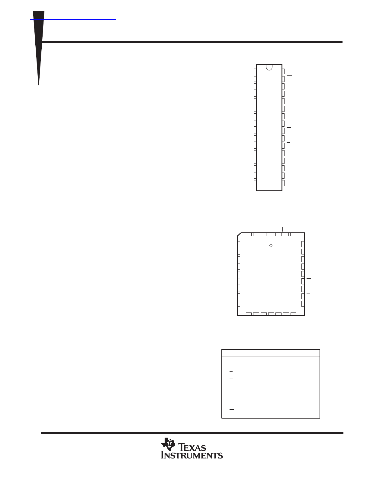
The TMS28F010A Flash EEPROM is offered in a
dual in-line plastic package (N suffix) designed for
insertion in mounting-hole rows on 15,2-mm
(600-mil) centers, a 32-lead plastic leaded
chip-carrier package using 1,25-mm (50-mil) lead
spacing (FM suffix), a 32-lead thin small-outline
package (DD suffix), and a reverse pinout TSOP
package (DU suffix).
A7
A6
A5
A4
A3
A2
A1
A0
DQ0
N PACKAGE
(TOP VIEW)
V
1
PP
A16
2
A15
3
A12
4
A7
5
A6
6
A5
7
A4
8
A3
9
A2
10
A1
11
A0
12
DQ0
13
DQ1
14
DQ2
15
V
16
SS
FM PACKAGE
(TOP VIEW)
A12
A15
A16
3213231
430
5
6
7
8
9
10
11
12
13
14
15 16 17 18 19
SS
DQ1
DQ2
V
32
31
30
29
28
27
26
25
24
23
22
21
20
19
18
17
PPVCC
V
DQ3
DQ4
V
CC
W
NC
A14
A13
A8
A9
A1 1
G
A10
E
DQ7
DQ6
DQ5
DQ4
DQ3
W
20
DQ5
NC
29
28
27
26
25
24
23
22
21
DQ6
A14
A13
A8
A9
A1 1
G
A10
E
DQ7
The TMS28F010A is characterized for operation
in temperature ranges of 0°C to 70°C (NL, FML,
DDL, and DUL suffixes), –40°C to 85°C (NE, FME,
DDE, and DUE suffixes), and –40°C to 125°C
(NQ, FMQ, DDQ, and DUQ suffixes). All package
types are offered with 168-hour burn-in (4 suffix).
PRODUCTION DATA information is current as of publication date.
Products conform to specifications per the terms of Texas Instruments
standard warranty. Production processing does not necessarily include
testing of all parameters.
POST OFFICE BOX 655303 • DALLAS, TEXAS 75265
POST OFFICE BOX 1443
A0–A16 Address Inputs
DQ0–DQ7 Data In/Data Out
E
G
NC No Internal Connection
V
CC
V
PP
V
SS
W
• HOUSTON, TEXAS 77251–1443
PIN NOMENCLATURE
Chip Enable
Output Enable
5-V Power Supply
12-V Power Supply
Ground
Write Enable
Copyright 1993, Texas Instruments Incorporated
1
Page 2

TMS28F010A
1048576-BIT FLASH
ELECTRICALLY ERASABLE PROGRAMMABLE READ-ONLY MEMORY
SMJS012 – DECEMBER 1992 – REVISED NOVEMBER 1993
DD PACKAGE
(TOP VIEW)
A11
A9
A8
A13
A14
NC
W
V
CC
V
PP
A16
A15
A12
A7
A6
A5
A4
A10
DQ7
DQ6
DQ5
DQ4
DQ3
V
SS
DQ2
DQ1
DQ0
A0
A1
A2
A3
32
31
30
29
28
27
26
25
24
23
22
21
20
19
18
17
32
31
30
29
28
27
26
25
24
23
22
21
20
19
18
17
G
A10
E
DQ7
DQ6
DQ5
DQ4
DQ3
V
SS
DQ2
DQ1
DQ0
A0
A1
A2
A3
A1 1
A9
A8
A13
A14
NC
W
V
CC
V
PP
A16
A15
A12
A7
A6
A5
A4
1
2
3
4
5
6
7
8
9
10
11
12
13
14
15
16
DU PACKAGE
REVERSE PINOUT
(TOP VIEW)
1
G
2
3
E
4
5
6
7
8
9
10
11
12
13
14
15
16
2
POST OFFICE BOX 655303 • DALLAS, TEXAS 75265
POST OFFICE BOX 1443
• HOUSTON, TEXAS 77251–1443
Page 3

ELECTRICALLY ERASABLE PROGRAMMABLE READ-ONLY MEMORY
device symbol nomenclature
-12 C4 FM L 4TMS28F010A
TMS28F010A
1048576-BIT FLASH
SMJS012 – DECEMBER 1992 – REVISED NOVEMBER 1993
PEP4 Burn-In
4 = 168-Hour Burn-In
(blank if no burn-in)
Temperature Range Designator
L= 0°Cto70°C
E=–40°Cto85°C
Q=–40°C to 125°C
Package Designator
N = Plastic Dual In-Line Package
FM = Plastic Leaded Chip Carrier
DD = Thin Small-Outline Package
DU = Thin Small-Outline Package,
Reverse Pinout
Program/Erase Endurance
C4 = 10 000 Cycles
C3 = 1 000 Cycles
Speed Designator
-10 = 100 ns
-12 = 120 ns
-15 = 150 ns
-17 = 170 ns
POST OFFICE BOX 655303 • DALLAS, TEXAS 75265
POST OFFICE BOX 1443
• HOUSTON, TEXAS 77251–1443
3
Page 4
TMS28F010A
1048576-BIT FLASH
ELECTRICALLY ERASABLE PROGRAMMABLE READ-ONLY MEMORY
SMJS012 – DECEMBER 1992 – REVISED NOVEMBER 1993
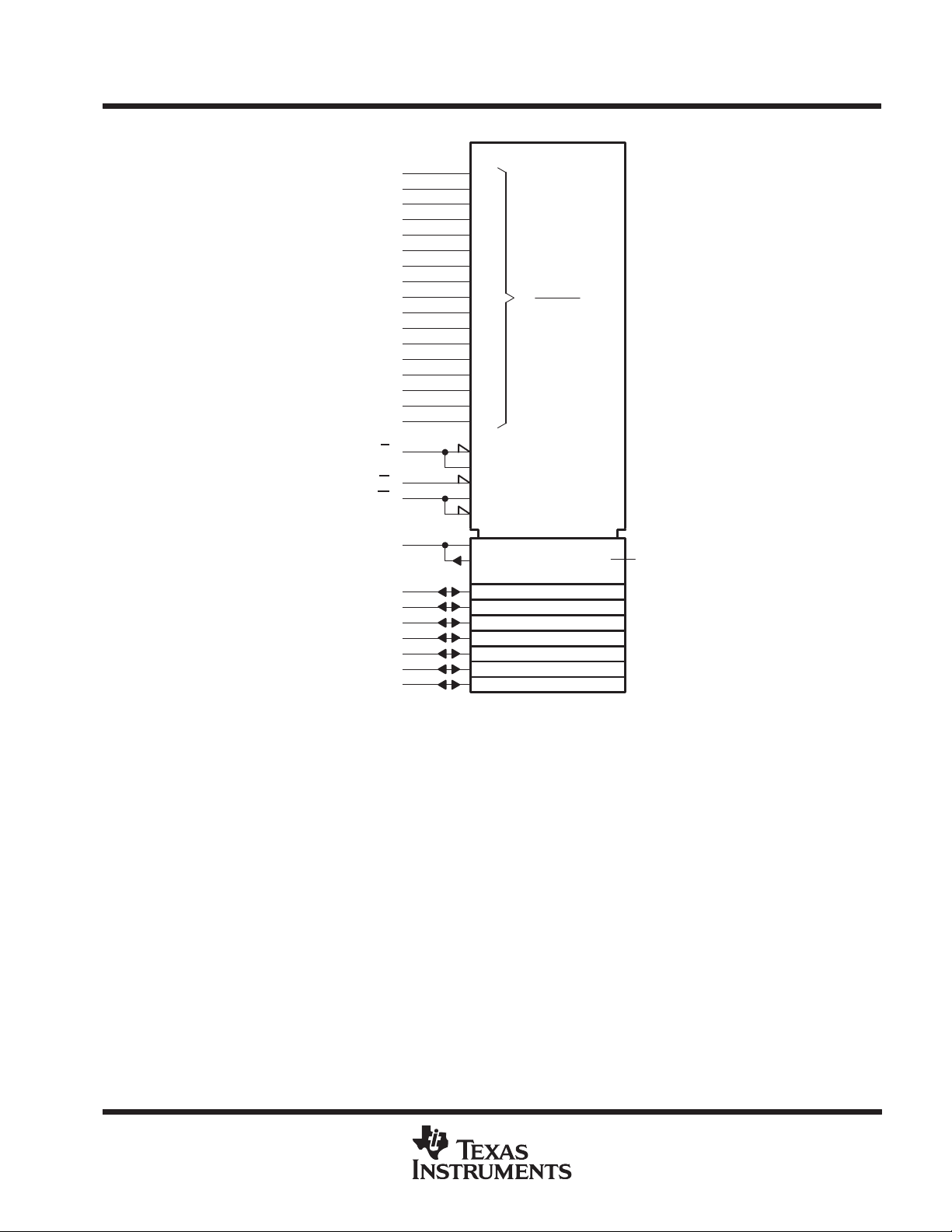
logic symbol
†
This symbol is in accordance with ANSI/IEEE Std 91-1984 and IEC Publication 617-12.
Pin numbers shown are for the N package.
†
FLASH
EEPROM
131 072 × 8
0
A
131 071
A0
A1
A2
A3
A4
A5
A6
A7
A8
A9
A10
A11
A12
A13
A14
A15
A16
DQ0
DQ1
DQ2
DQ3
DQ4
DQ5
DQ6
DQ7
12
11
10
9
8
7
6
5
27
26
23
25
4
28
29
3
2
22
E
24
G
31
W
13
14
15
17
18
19
20
21
0
16
G1
[PWR DWN]
G2
1, 2 EN (READ)
1C3 (WRITE)
A, 3D
∇ 4
A, Z4
4
POST OFFICE BOX 655303 • DALLAS, TEXAS 75265
POST OFFICE BOX 1443
• HOUSTON, TEXAS 77251–1443
Page 5
ELECTRICALLY ERASABLE PROGRAMMABLE READ-ONLY MEMORY
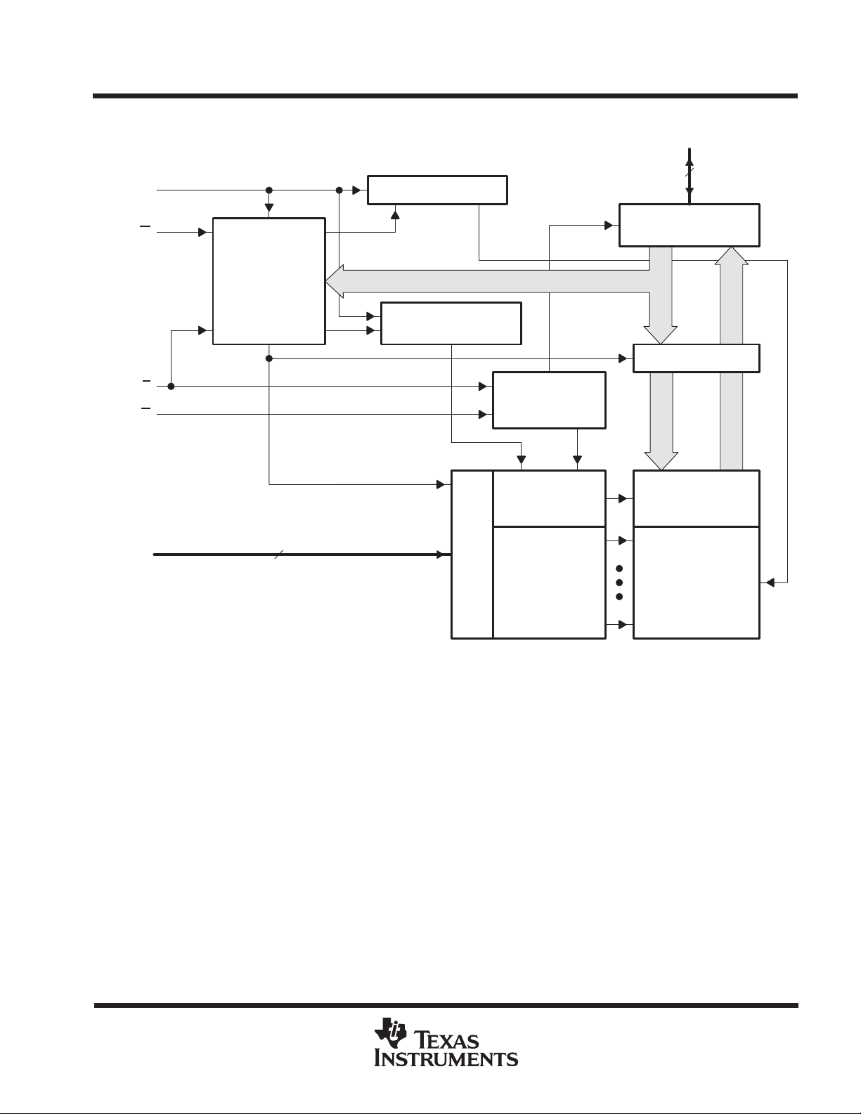
functional block diagram
TMS28F010A
1048576-BIT FLASH
SMJS012 – DECEMBER 1992 – REVISED NOVEMBER 1993
DQ0–DQ7
V
PP
A0–A16
Erase-Voltage Switch
W
E
G
State Control
Program/Erase
Stop Timer
Command Register
17
To Array
Program-Voltage
Switch
STB
A
d
d
r
e
s
s
L
a
t
c
h
STB
Chip-Enable and
Output-Enable
Logic
Column Decoder
Row Decoder
Input/Output Buffers
8
Data Latch
Column Gating
1048576-Bit
Array Matrix
POST OFFICE BOX 655303 • DALLAS, TEXAS 75265
POST OFFICE BOX 1443
• HOUSTON, TEXAS 77251–1443
5
Page 6
TMS28F010A
Algorithm-Selection Mode
V
VILV
VIDV
IDENTIFIER
1048576-BIT FLASH
ELECTRICALLY ERASABLE PROGRAMMABLE READ-ONLY MEMORY
SMJS012 – DECEMBER 1992 – REVISED NOVEMBER 1993
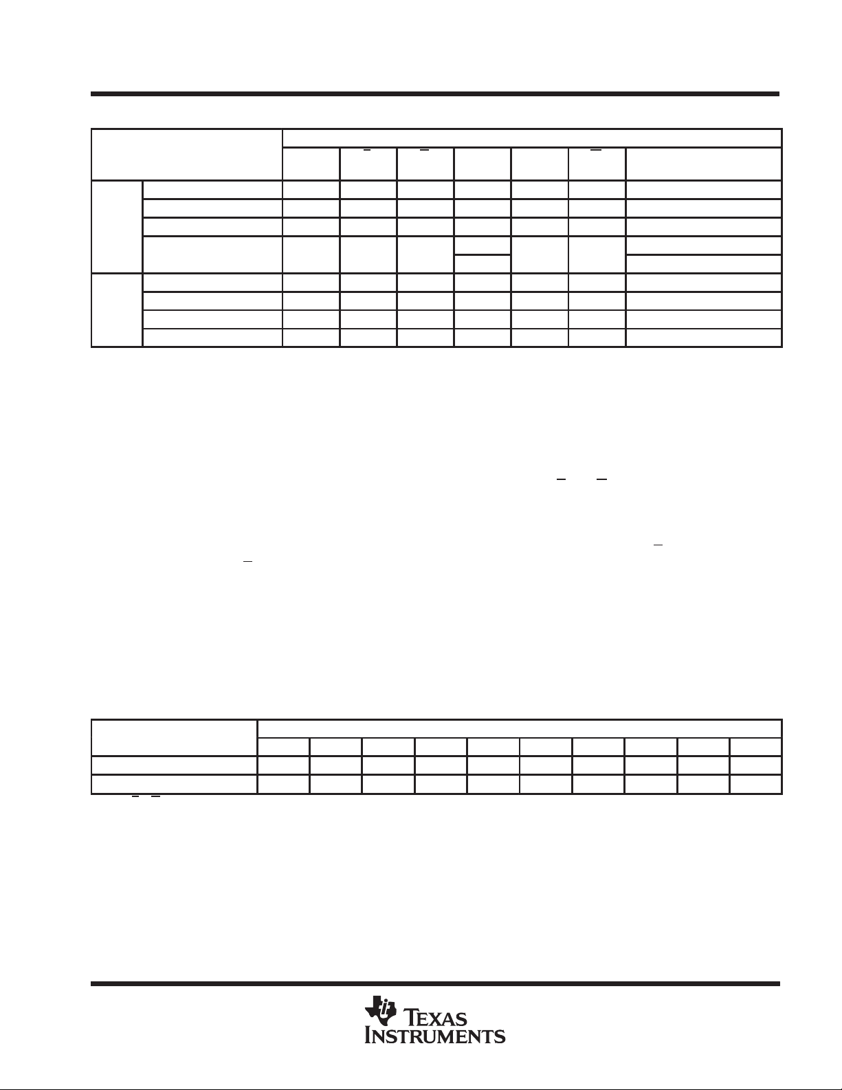
Table 1. Operation Modes
FUNCTION
MODE
Read V
Output Disable V
Read
Read/
Write
NOTE: X can be VIL or VIH.
†
V
PPL
Standby and Write Inhibit V
Read V
Output Disable V
Standby and Write Inhibit V
Write V
≤ VCC + 2 V; V
PPH
operation
read/output disable
is the programming voltage specified for the device. For more details, refer to the recommended operating conditions.
V
PP
(1)
PPL
PPL
PPL
PPL
PPH
PPH
PPH
PPH
†
E
(22)
V
V
V
IH
V
V
V
IH
V
G
(24)
IL
IL
IL
IL
IL
V
IL
V
IH
X X X
IL
V
IL
V
IH
X X X
V
IH
A0
(12)
X X
X X
V
IL
V
IH
X X
X X
X X
A9
(26)
W
(31)
V
IH
V
IH
X
IH
V
IH
V
IH
X
V
IL
DQ0–DQ7
(13–15, 17–21)
Data Out
HI-Z
HI-Z
Mfr Equivalent Code 89h
Device Equivalent Code B4h
Data Out
HI-Z
HI-Z
Data In
When the outputs of two or more TMS28F010As are connected in parallel on the same bus, the output of any
particular device in the circuit can be read with no interference from the competing outputs of other devices. T o
read the output of the TMS28F010A, a low-level signal is applied to the E
and G pins. All other devices in the
circuit should have their outputs disabled by applying a high-level signal to one of these pins.
standby and write inhibit
Active I
high CMOS level on E
current can be reduced from 30 mA to 1 mA by applying a high TTL level on E or to 100 µA with a
CC
. In this mode, all outputs are in the high-impedance state. The TMS28F010A draws active
current when it is deselected during programming, erasure, or program/erase verification. It continues to draw
active current until the operation is terminated.
algorithm-selection mode
The algorithm-selection mode provides access to a binary code identifying the correct programming and erase
agorithms. This mode is activated when A9 (pin 26) is forced to V
A0. All other addresses must be held low.
A0 low selects the manufacturer equivalent code 89h, and A0 high
. Two identifier bytes are accessed by toggling
ID
selects the device equivalent code B4h, as shown in the algorithm-selection mode table below:
PINS
A0 DQ7 DQ6 DQ5 DQ4 DQ3 DQ2 DQ1 DQ0 HEX
Manufacturer Equivalent Code V
Device Equivalent Code V
NOTE: E = G = VIL, A1–A8 = VIL, A9 = VID, A10–A16 = VIL, VPP = V
IL
IH
1 0 0 0 1 0 0 1 89
1 0 1 1 0 1 0 0 B4
.
PPL
programming and erasure
In the erased state, all bits are at a logic 1. Before erasing the device, all memory bits must be programmed to
a logic 0. Afterwards, the entire chip is erased. At this point, the bits, now logic 1s, can be programmed
accordingly. Refer to the Fastwrite and Fasterase algorithms for further detail.
6
POST OFFICE BOX 655303 • DALLAS, TEXAS 75265
POST OFFICE BOX 1443
• HOUSTON, TEXAS 77251–1443
Page 7
TMS28F010A
COMMAND
BUS
1048576-BIT FLASH
ELECTRICALLY ERASABLE PROGRAMMABLE READ-ONLY MEMORY
SMJS012 – DECEMBER 1992 – REVISED NOVEMBER 1993
command register
The command register controls the program and erase functions of the TMS28F010A. The algorithm-selection
mode can be activated using the command register in addition to the above method. When V
contents of the command register and the function being performed can be changed. The command register
is written to when E
is low and W is pulsed low. The address is latched on the leading edge of the pulse, while
the data is latched on the trailing edge. Accidental programming or erasure is minimized because two
commands must be executed to invoke either operation.
power supply considerations
PP
is high, the
Each device should have a 0.1-µF ceramic capacitor connected between V
Changes in current drain on V
require it to have a bypass capacitor as well. Printed-circuit traces for both
PP
and VSS to suppress circuit noise.
CC
power supplies should be appropriate to handle the current demand.
Table 2. Command Definitions
REQUIRED
CYCLES
Read 1 Write X 00h Read RA RD
Algorithm-Selection Mode 3 Write X 90h Read
Set-Up-Erase/Erase 2 Write X 20h Write X 20h
Erase Verify 2 Write EA A0h Read X EVD
Set-Up-Program/Program 2 Write X 40h Write PA PD
Program Verify 2 Write X C0h Read X PVD
Reset 2 Write X FFh Write X FFh
†
Modes of operation are defined in Table 1.
Legend:
EA Address of memory location to be read during erase verify.
RA Address of memory location to be read.
PA Address of memory location to be programmed. Address is latched on the falling edge of W
RD Data read from location RA during the read operation.
EVD Data read from location EA during erase verify.
PD Data to be programmed at location PA. Data is latched on the rising edge of W
PVD Data read from location PA during program verify.
OPERATION†ADDRESS DATA OPERATION†ADDRESS DATA
FIRST BUS CYCLE SECOND BUS CYCLE
0000
0001
.
.
89h
B4h
POST OFFICE BOX 655303 • DALLAS, TEXAS 75265
POST OFFICE BOX 1443
• HOUSTON, TEXAS 77251–1443
7
Page 8

TMS28F010A
1048576-BIT FLASH
ELECTRICALLY ERASABLE PROGRAMMABLE READ-ONLY MEMORY
SMJS012 – DECEMBER 1992 – REVISED NOVEMBER 1993
command definitions
read command
Memory contents can be accessed while V
register invokes the read operation. When the device is powered up, the default contents of the command
register are 00h and the read operation is enabled. The read operation remains enabled until a different valid
command is written to the command register.
algorithm-selection mode command
The algorithm-selection mode is activated by writing 90h into the command register. The manufacturer
equivalent code (89h) is identified by the value read from address location 0000h, and the device equivalent
code (B4h) is identified by the value read from address location 0001h.
set-up-erase/erase commands
The erase-algorithm initiates with E
write the set-up-erase command, 20h, into the command register. After the TMS28F010A is in the erase mode,
writing a second erase command, 20h, into the command register invokes the erase operation. The erase
operation begins on the rising edge of W
10 ms to complete before the erase-verify command, A0h, can be loaded.
Maximum erase timing is controlled by the internal stop timer. When the stop timer terminates the erase
operation, the device enters an inactive state and remains inactive until a valid erase verify, read, or reset
command is received.
erase-verify command
All bytes must be verified following an erase operation. After the erase operation is complete, an erased byte
can be verified by writing the erase-verify command, A0h, into the command register. This command causes
the device to exit the erase mode on the rising edge of W
the falling edge of W
command register.
. The erase-verify operation remains enabled until a valid command is written to the
= VIL, W = VIL, G = VIH, VPP = V
is high or low. When VPP is high, writing 00h into the command
PP
, and VCC = 5 V . T o enter the erase mode,
PPH
and ends on the rising edge of the next W. The erase operation requires
. The address of the byte to be verified is latched on
T o determine whether or not all the bytes have been erased, the TMS28F010A applies a margin voltage to each
byte. If FFh is read from the byte, all bits in the designated byte have been erased. The erase-verify operation
continues until all of the bytes have been verified. If FFh is not read from a byte, an additional erase operation
needs to be executed. Figure 2 shows the combination of commands and bus operations for electrically erasing
the TMS28F010A.
set-up-program/program commands
The programming algorithm initiates with E
programming mode, write the set-up-program command, 40h, into the command register. The programming
operation is invoked by the next write-enable pulse. Addresses are latched internally on the falling edge of W
and data is latched internally on the rising edge of W
and ends on the rising edge of the next W pulse. The program operation requires 10 µs for completion before
W
the program-verify command, C0h, can be loaded.
Maximum program timing is controlled by the internal stop timer. When the stop timer terminates the program
operation, the device enters an inactive state and remains inactive until a valid program-verify, read, or reset
command is received.
= VIL, W = VIL, G = VIH, VPP = V
. The programming operation begins on the rising edge of
, and VCC = 5 V . To enter the
PPH
,
8
POST OFFICE BOX 655303 • DALLAS, TEXAS 75265
POST OFFICE BOX 1443
• HOUSTON, TEXAS 77251–1443
Page 9

TMS28F010A
1048576-BIT FLASH
ELECTRICALLY ERASABLE PROGRAMMABLE READ-ONLY MEMORY
SMJS012 – DECEMBER 1992 – REVISED NOVEMBER 1993
program-verify command
The TMS28F010A can be programmed sequentially or randomly because it is programmed one byte at a time.
Each byte must be verified after it is programmed. The program-verify operation prepares the device to verify
the most recently programmed byte. To invoke the program-verify operation, C0h must be written into the
command register. The program-verify operation ends on the rising edge of W
While verifying a byte, the TMS28F010A applies an internal margin voltage to the designated byte. If the true
data and programmed data match, programming continues to the next designated byte location; otherwise, the
byte must be reprogrammed. Figure 1 shows how commands and bus operations are combined for byte
programming.
reset command
To reset the TMS28F010A after set-up-erase command or set-up-program command operations without
changing the contents in memory , write FFh into the command register two consecutive times. After executing
the reset command, a valid command must be written into the command register to change to a new state.
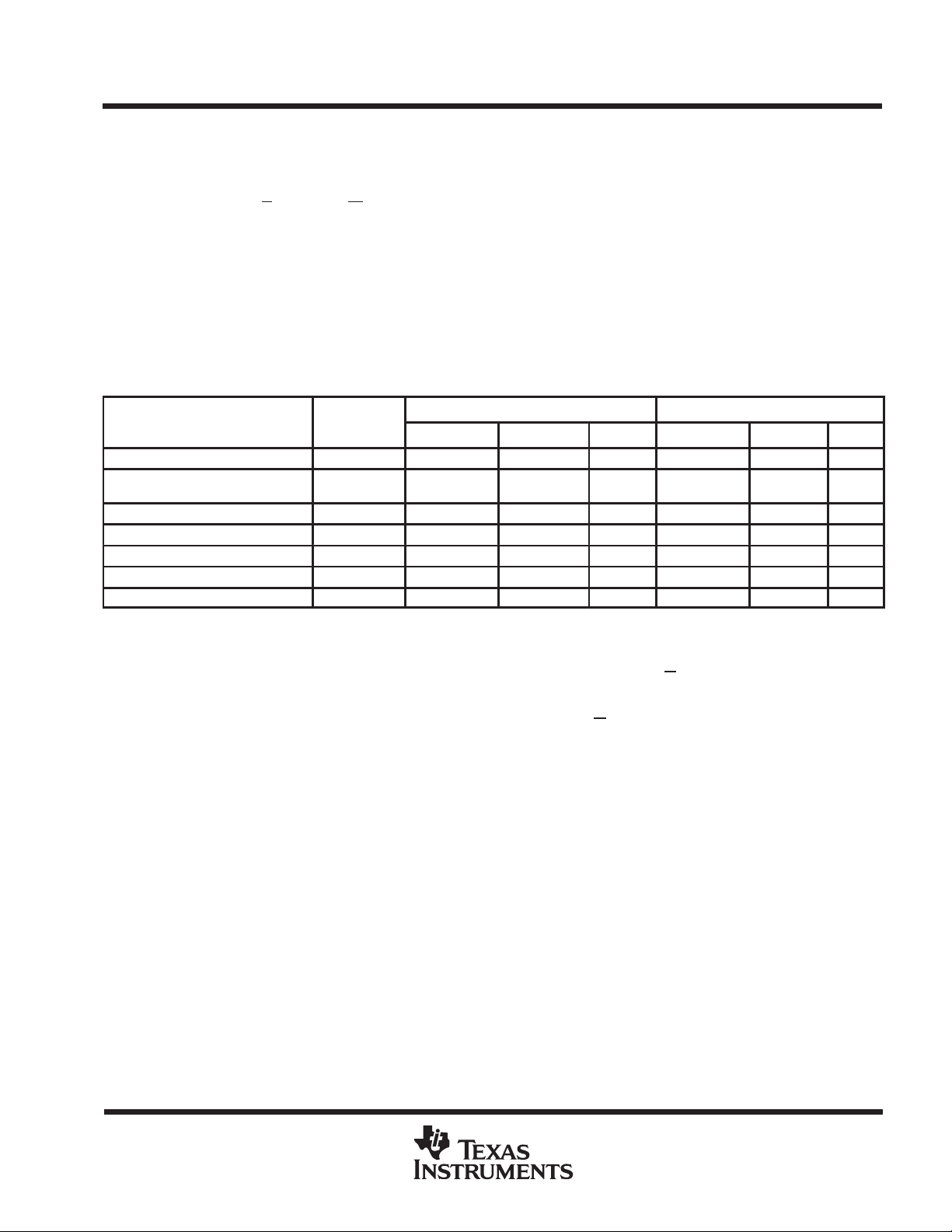
Fastwrite algorithm
The TMS28F010A is programmed using the Texas Instruments Fastwrite algorithm shown in Figure 1. This
algorithm programs in a nominal time of two seconds.
.
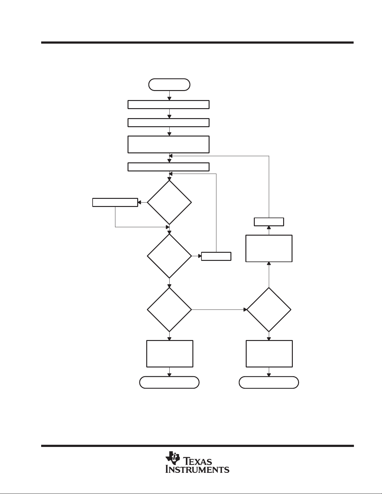
Fasterase algorithm
The TMS28F010A is erased using the T exas Instruments Fasterase algorithm shown in Figure 2. The memory
array needs to be completely programmed (using the Fastwrite algorithm) before erasure begins. Erasure
typically occurs in one second.
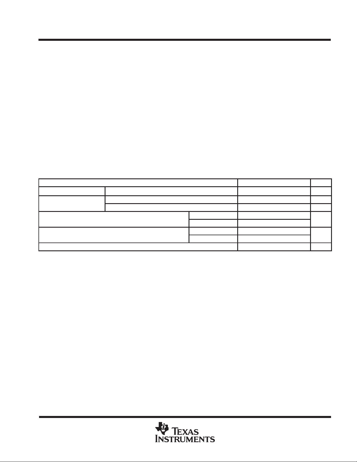
parallel erasure
To reduce total erase time, several devices can be erased in parallel. Since each Flash EEPROM can erase
at a different rate, every device must be verified separately after each erase pulse. After a given device has been
successfully erased, the erase command should not be issued to this device again. All devices that complete
erasure should be masked until the parallel erasure process is finished (see Figure 3).
Examples of how to mask a device during parallel erase include driving the E
(00h) to the device when the others receive a set-up-erase or erase command, or disconnecting it from all
electrical signals with relays or other types of switches.
pin high, writing the read command
POST OFFICE BOX 655303 • DALLAS, TEXAS 75265
POST OFFICE BOX 1443
• HOUSTON, TEXAS 77251–1443
9
Page 10

TMS28F010A
1048576-BIT FLASH
ELECTRICALLY ERASABLE PROGRAMMABLE READ-ONLY MEMORY
SMJS012 – DECEMBER 1992 – REVISED NOVEMBER 1993
Increment
Address
Start
Address = 00h
VCC = 5 V ± 10%, VPP = 12 V ± 5%
X = 1
Write Set-Up-Program Command
Write Data
Wait = 10µs
Write Program-Verify Command
Wait = 6 µs
Read
and Verify
Byte
Fail
Pass
X = X + 1
No
X = 25?
Yes
Setup
Interactive
Mode
Bus
Operation
Initialize
Address
Standby
Write
Write
Standby
Write
Standby
Read
Command Comments
Wait for VPP to ramp to
V
(see Note A)
PPH
Initialize pulse count
Set-UpProgram
Write
Write Data Valid address/data
ProgramVerify
Data = 40h
Wait = 10 µs
Data = C0h; ends
Program operation
Wait = 6 µs
Read byte to verify
Programming; compare
output to expected output
No
Write Read Command
NOTES: A. Refer to the recommended operating conditions for the value of V
B. Refer to the recommended operating conditions for the value of V
Last
Address
?
Yes
Apply V
PPL
Device Passed
Apply V
PPL
Device Failed
Power
Down
Figure 1. Programming Flowchart: Fastwrite Algorithm
Write
Standby
PPH.
PPL
Read Data = 00h; resets register
.
for read operations
Wait for VPP to ramp to
V
(see Note B)
PPL
10
POST OFFICE BOX 655303 • DALLAS, TEXAS 75265
POST OFFICE BOX 1443
• HOUSTON, TEXAS 77251–1443
Page 11

TMS28F010A
1048576-BIT FLASH
ELECTRICALLY ERASABLE PROGRAMMABLE READ-ONLY MEMORY
SMJS012 – DECEMBER 1992 – REVISED NOVEMBER 1993
Start
All Bytes = 00h
?
Yes
Address = 00h
VCC = 5 V ± 10%, VPP = 12 V ± 5%
X = 1
Write Set-Up-Erase Command
Write-Erase Command
Wait = 10 ms
Write Erase-Verify Command
No
Program All
Bytes to 00h
X = X + 1
Preprogram
Setup
Interactive
Mode
Bus
Operation
Standby
Write
Write
Command Comments
Entire memory must = 00h
before erasure
Use Fastwrite
programming algorithm
Initialize addresses
Wait for VPP to ramp to
V
(see Note A)
PPH
Initialize pulse count
Set-UpErase
Erase Data = 20h
Data = 20h
Increment
Address
Wait = 6 µs
Read
and Verify
Byte
No
Last
Address?
Write Read Command
Apply V
Device Passed Device Failed
Fail
Pass
Yes
PPL
X = 1000?
Apply V
No
Yes
PPL
Power
Down
Standby
Write
Standby
Read
Write
Standby
Wait = 10 ms
Erase
Verify
Read Data = 00h; resets register
Addr = Byte to verify;
Data = A0h; ends the erase
operation
Wait = 6 µs
Read byte to verify erasure;
compare output to FFh
for read operations
Wait for VPP to ramp to
V
(see Note B)
PPL
POST OFFICE BOX 655303 • DALLAS, TEXAS 75265
POST OFFICE BOX 1443
• HOUSTON, TEXAS 77251–1443
11
Page 12
TMS28F010A
1048576-BIT FLASH
ELECTRICALLY ERASABLE PROGRAMMABLE READ-ONLY MEMORY
SMJS012 – DECEMBER 1992 – REVISED NOVEMBER 1993
NOTES: A. Refer to the recommended operating conditions for the value of V
B. Refer to the recommended operating conditions for the value of V
Figure 2. Flash-Erase Flowchart: Fasterase Algorithm
Start
Program All Devices to 00h
X = 1
Give Erase Command to All
Mask Device #D
Yes
Devices
D = 1
Is
Device #D
Erased
?
No
PPH.
PPL
.
X = X+1
NOTE: n = number of devices being erased.
D = n
?
Are
All Devices
Erased
?
Give Read
Command to
All Devices
All Devices Pass
No
D = D+1
Yes
No
Yes
Finished With Errors
Figure 3. Parallel-Erase Flow Diagram
Give Erase
Command to
All Unmasked
Devices
No
X = 1000
?
Yes
Give Read
Command to
All Devices
12
POST OFFICE BOX 655303 • DALLAS, TEXAS 75265
POST OFFICE BOX 1443
• HOUSTON, TEXAS 77251–1443
Page 13
TMS28F010A
VCCSuppl
oltage
During write/read/flash erase
4.555.5
V
VPPSuppl
oltage
VIHHigh-level dc input
oltage
V
VILLow-level dc input voltage
V
1048576-BIT FLASH
ELECTRICALLY ERASABLE PROGRAMMABLE READ-ONLY MEMORY
SMJS012 – DECEMBER 1992 – REVISED NOVEMBER 1993
absolute maximum ratings over operating free-air temperature range (unless otherwise noted)
Supply voltage range, V
Supply voltage range, V
Input voltage range (see Note 2): All inputs except A9 –0.6 V to V
Output voltage range (see Note 3) –0.6 V to V
Operating free-air temperature range during read/erase/program, T
Storage temperature range –65°C to 150°C. . . . . . . . . . . . . . . . . . . . . . . . . . . . . . . . . . . . . . . . . . . . . . . . . . . . . . .
†
Stresses beyond those listed under “absolute maximum ratings” may cause permanent damage to the device. These are stress ratings only and
functional operation of the device at these or any other conditions beyond those indicated under “recommended operating conditions” is not
implied. Exposure to absolute-maximum-rated conditions for extended periods may affect device reliability.
NOTES: 1. All voltage values are with respect to VSS.
2. The voltage on any input pin can undershoot to –2.0 V for periods less than 20 ns.
3. The voltage on any output pin can overshoot to 7.0 V for periods less than 20 ns.
(see Note 1) –0.6 V to 7 V. . . . . . . . . . . . . . . . . . . . . . . . . . . . . . . . . . . . . . . . . . . . . .
CC
–0.6 V to 14 V. . . . . . . . . . . . . . . . . . . . . . . . . . . . . . . . . . . . . . . . . . . . . . . . . . . . . . . . .
PP
A9 –0.6 V to 13.5 V. . . . . . . . . . . . . . . . . . . . . . . . . . . . . . . . . . . . . . . . . . . . . . .
NL, FML, DDL, DUL 0°C to 70°C. . . . . . . . . . . . . . . . . . . . . . . . . . . . . . . . . . .
A
NE, FME, DDE, DUE – 40°C to 85°C. . . . . . . . . . . . . . . . . . . . . . . . . . . . . . .
NQ, FMQ, DDQ, DUQ – 40° C to 125°C. . . . . . . . . . . . . . . . . . . . . . . . . . . . .
CC
CC
+ 1 V. . . . . . . . . . . . . . . . . . . . . . . . . . . .
+ 1 V. . . . . . . . . . . . . . . . . . . . . . . . . . . . . . . . . . . . . . . . . . . . .
recommended operating conditions
MIN TYP MAX UNIT
pp
y v
pp
y v
p
p
V
Voltage level on A9 for algorithm-selection mode 11.5 13 V
ID
During read only (V
During write/read/flash erase (V
v
) 0 VCC + 2 V
PPL
) 11.4 12 12.6 V
PPH
TTL 2 VCC+0.5
CMOS VCC– 0.5 VCC+0.5
TTL –0.5 0.8
CMOS GND – 0.2 GND+0.2
†
POST OFFICE BOX 655303 • DALLAS, TEXAS 75265
POST OFFICE BOX 1443
• HOUSTON, TEXAS 77251–1443
13
Page 14

TMS28F010A
VOHHigh-level output voltage
V
VOLLow-level output voltage
V
IIInput current (leakage)
A
I
V
pply current (read/standby)
I
pply current (standby)
1048576-BIT FLASH
ELECTRICALLY ERASABLE PROGRAMMABLE READ-ONLY MEMORY
SMJS012 – DECEMBER 1992 – REVISED NOVEMBER 1993
electrical characteristics over recommended ranges of supply voltage and operating free-air
temperature
PARAMETER TEST CONDITIONS MIN MAX UNIT
p
p
I
ID
I
O
PP1
I
PP2
I
PP3
I
PP4
CCSVCC
I
CC1
I
CC2
I
CC3
I
CC4
NOTE 4: Not 100% tested; characterization data available.
A9 algorithm-selection-mode current A9 = VID max 200 µA
p
Output current (leakage) VO = 0 V to V
pp
su
PP
VPP supply current (during program pulse) (see Note 4) VPP = V
VPP supply current (during flash erase) (see Note 4) VPP = V
VPP supply current (during program/erase verify)
(see Note 4)
pp
su
VCC supply current (active read)
VCC average supply current (active write) (see Note 4)
VCC average supply current (flash erase) (see Note 4)
VCC average supply current (program/erase verify)
(see Note 4)
All except A9 VI = 0 V to 5.5 V ±1
A9 VI = 0 V to 13 V ±200
TTL-input level VCC = 5.5 V, E = V
CMOS-input level VCC = 5.5 V, E = V
IOH = – 2.5 mA 2.4
IOH = – 100 µA VCC– 0.4
IOL = 5.8 mA 0.45
IOL = 100 µA 0.1
CC
VPP = V
VPP = V
VPP = V
VCC = 5.5 V E = VIL,
f = 6 MHz, Outputs open
VCC = 5.5 V, E = VIL,
Programming in progress
VCC = 5.5 V, E = VIL,
Erasure in progress
VCC = 5.5 V, E = VIL,
VPP = V
Program/erase-verify in progress
, Read mode 200 µA
PPH
PPL
PPH
PPH
PPH
IH
CC
,
PPH
±10 µA
±10 µA
30 mA
30 mA
5.0 mA
100 µA
30 mA
10 mA
15 mA
15 mA
µ
1 mA
capacitance over recommended ranges of supply voltage and operating free-air temperature,
f = 1 MHz
C
i
C
o
†
Capacitance measurements are made on sample basis only.
†
PARAMETER TEST CONDITIONS MIN MAX UNIT
Input capacitance VI = 0 , f = 1 MHz 6 pF
Output capacitance VO = 0, f = 1 MHz 12 pF
14
POST OFFICE BOX 655303 • DALLAS, TEXAS 75265
POST OFFICE BOX 1443
• HOUSTON, TEXAS 77251–1443
Page 15

TMS28F010A
PARAMETER
UNIT
L
I
t
1048576-BIT FLASH
ELECTRICALLY ERASABLE PROGRAMMABLE READ-ONLY MEMORY
SMJS012 – DECEMBER 1992 – REVISED NOVEMBER 1993
switching characteristics over recommended ranges of supply voltage and operating free-air
temperature
t
a(A)
t
a(E)
t
en(G)
t
c(R)
t
d(E)
t
d(G)
t
dis(E)
t
dis(G)
t
h(D)
t
rec(W)
†
Whichever occurs first.
Access time from
address, A0–A16
Access time from
chip enable, E
Access time from
output enable, G
Cycle time, read t
Delay time, E low
to low-Z output
Delay time, G low
to low-Z output
Chip disable time
to hi-Z output
Output disable
time to hi-Z
output
Hold time, data
valid from
address, E
Write recovery
time before read
, or G
TEST ALTERNATE
CONDITIONS SYMBOL
CL = 100 pF,
1 Series 74
TTL load,
p
nput
≤ 20 ns,
r
Input tf ≤ 20 ns
†
t
AVQV
t
ELQV
t
GLQV
AVAV
t
ELQX
t
GLQX
t
EHQZ
t
GHQZ
t
AXQX
t
WHGL
’28F010A-10 ’28F010A-12 ’28F010A-15 ’28F010A-17
MIN MAX MIN MAX MIN MAX MIN MAX
100 120 150 170 ns
100 120 150 170 ns
45 50 55 60 ns
100 120 150 170 ns
0 0 0 0 ns
0 0 0 0 ns
0 55 0 55 0 55 0 55 ns
0 30 0 30 0 35 0 35 ns
0 0 0 0 ns
6 6 6 6 µs
POST OFFICE BOX 655303 • DALLAS, TEXAS 75265
POST OFFICE BOX 1443
• HOUSTON, TEXAS 77251–1443
15
Page 16

TMS28F010A
’28F010A-10
’28F010A-12
PARAMETER
UNIT
’28F010A-15
’28F010A-17
PARAMETER
UNIT
1048576-BIT FLASH
ELECTRICALLY ERASABLE PROGRAMMABLE READ-ONLY MEMORY
SMJS012 – DECEMBER 1992 – REVISED NOVEMBER 1993
timing requirements–write/erase/program operations
t
c(W)
t
c(W)PR
t
c(W)ER
t
h(A)
t
h(E)
t
h(WHD)
t
su(A)
t
su(D)
t
su(E)
t
su(EHVPP)
t
su(VPPEL)
t
rec(W)
t
rec(R)
t
w(W)
t
w(WH)
t
r(VPP)
t
f(VPP)
t
c(W)
t
c(W)PR
t
c(W)ER
t
h(A)
t
h(E)
t
h(WHD)
t
su(A)
t
su(D)
t
su(E)
t
su(EHVPP)
t
su(VPPEL)
t
rec(W)
t
rec(R)
t
w(W)
t
w(WH)
t
r(VPP)
t
f(VPP)
NOTE 5: Rise/fall time ≤ 10 ns.
Cycle time, write using W t
Cycle time, programming operation t
Cycle time, erase operation t
Hold time, address t
Hold time, E t
Hold time, data valid after W high t
Setup time, address t
Setup time, data t
Setup time, E before W t
Setup time, E high to VPP ramp t
Setup time, VPP to E low t
Recovery time, W before read t
Recovery time, read before W t
Pulse duration, W (see Note 5) t
Pulse duration, W high t
Rise time, V
Fall time, V
PP
PP
PP
PP
ALTERNA TE
SYMBOL
AVAV
WHWH1
WHWH2
WLAX
WHEH
WHDX
AVWL
DVWH
ELWL
EHVP
VPEL
WHGL
GHWL
WLWH
WHWL
t
VPPR
t
VPPF
ALTERNATE
SYMBOL
AVAV
WHWH1
WHWH2
WLAX
WHEH
WHDX
AVWL
DVWH
ELWL
EHVP
VPEL
WHGL
GHWL
WLWH
WHWL
t
VPPR
t
VPPF
’
MIN NOM MAX MIN NOM MAX
100 120 ns
10 10 µs
9.5 10 9.5 10 ms
55 60 ns
0 0 ns
10 10 ns
0 0 ns
50 50 ns
20 20 ns
100 100 ns
1.0 1.0 µs
6 6 µs
0 0 µs
60 60 ns
20 20 ns
1 1 µs
1 1 µs
’
MIN NOM MAX MIN NOM MAX
150 170 ns
10 10 µs
9.5 10 9.5 10 ms
60 70 ns
0 0 ns
10 10 ns
0 0 ns
50 50 ns
20 20 ns
100 100 ns
1.0 1.0 µs
6 6 µs
0 0 µs
60 60 ns
20 20 ns
1 1 µs
1 1 µs
’
’
16
POST OFFICE BOX 655303 • DALLAS, TEXAS 75265
POST OFFICE BOX 1443
• HOUSTON, TEXAS 77251–1443
Page 17

ELECTRICALLY ERASABLE PROGRAMMABLE READ-ONLY MEMORY
’28F010A-10
’28F010A-12
’28F010A-15
’28F010A-17
PARAMETER
UNIT
timing requirements — alternative E-controlled writes
TMS28F010A
1048576-BIT FLASH
SMJS012 – DECEMBER 1992 – REVISED NOVEMBER 1993
t
c(W)
t
c(E)PR
t
h(EA)
t
h(ED)
t
h(W)
t
su(A)
t
su(D)
t
su(W)
t
su(VPPEL)
t
rec(E)R
t
rec(E)W
t
w(E)
t
w(EH)
ALTERNA TE
Cycle time, write using E t
Cycle time, programming op-
eration
Hold time, address t
Hold time, data t
Hold time, W t
Setup time, address t
Setup time, data t
Setup time, W before E t
Setup time, VPP to E low t
Recovery time, write using E
before read
Recovery time, read before
write using E
Pulse duration, write using E t
Pulse duration, write, E high t
PARAMETER MEASUREMENT INFORMATION
SYMBOL
AVAV
t
EHEH
ELAX
EHDX
EHWH
AVEL
DVEH
WLEL
VPEL
t
EHGL
t
GHEL
ELEH
EHEL
’
MIN MAX MIN MAX MIN MAX MIN MAX
100 120 150 170 ns
10 10 10 10 µs
75 80 80 90 ns
10 10 10 10 ns
0 0 0 0 ns
0 0 0 0 ns
50 50 50 50 ns
0 0 0 0 ns
1.0 1.0 1.0 1.0 µs
6 6 6 6 µs
0 0 0 0 µs
70 70 70 80 ns
20 20 20 20 ns
’
’
’
2.08 V
RL = 800 Ω
Output
Under Test
CL = 100 pF
Figure 4. AC Test Output Load Circuit
AC testing input/output waveforms
2.4 V
0.45 V
2 V
0.8 V
AC testing inputs are driven at 2.4 V for logic high and 0.45 V for logic low. Timing measurements are made at
2 V for logic high and 0.8 V for logic low on both inputs and outputs. Each device should have a 0.1-µF ceramic
capacitor connected between V
and VSS as close as possible to the device pins.
CC
2 V
0.8 V
POST OFFICE BOX 655303 • DALLAS, TEXAS 75265
POST OFFICE BOX 1443
• HOUSTON, TEXAS 77251–1443
17
Page 18

TMS28F010A
1048576-BIT FLASH
ELECTRICALLY ERASABLE PROGRAMMABLE READ-ONLY MEMORY
SMJS012 – DECEMBER 1992 – REVISED NOVEMBER 1993
PARAMETER MEASUREMENT INFORMATION
t
c(R)
t
a(A)
Address Valid
t
a(E)
t
en(G)
t
d(G)
A0–A16
E
G
t
rec(W)
W
t
d(E)
DQ0–DQ7 Ouput Valid
HI-Z HI-Z
Figure 5. Read Cycle Timing
t
h(D)
t
dis(E)
t
dis(G)
18
POST OFFICE BOX 655303 • DALLAS, TEXAS 75265
POST OFFICE BOX 1443
• HOUSTON, TEXAS 77251–1443
Page 19

A0–A16
Power Up
and
Standby
TMS28F010A
1048576-BIT FLASH
ELECTRICALLY ERASABLE PROGRAMMABLE READ-ONLY MEMORY
SMJS012 – DECEMBER 1992 – REVISED NOVEMBER 1993
PARAMETER MEASUREMENT INFORMATION
Program
Set-Up-
Program
Command
Command
Latch
Address
and Data
Programming
Program
Verify
Command
Program
Verification
Standby/
Power Down
DQ0–DQ7
5 V
V
CC
0 V
V
PPH
V
PP
V
PPL
t
c(W)
t
su(A)
t
h(A)
E
t
su(E)
t
h(E)
G
t
rec(R)
W
t
h(WHD)
t
w(W)
t
su(D)
HI-Z
Data In = 40h
t
su(VPPEL)
t
r(VPP)
t
c(W)
t
su(E)
t
w(WH)
t
t
w(W)
t
su(D)
Data In
h(E)
t
c(W)PR
t
h(WHD)
t
c(W)
t
su(A)
t
t
w(W)
t
su(D)
Data In = C0h
t
h(A)
su(E)
t
rec(W)
t
t
h(E)
h(WHD)
t
d(E)
t
a(E)
t
c(R)
t
dis(E)
t
d(G)
t
dis(G)
t
h(D)
t
en(G)
Valid Data Out
t
f(VPP)
t
su(EHVPP)
Figure 6. Write Cycle Timing
POST OFFICE BOX 655303 • DALLAS, TEXAS 75265
POST OFFICE BOX 1443
• HOUSTON, TEXAS 77251–1443
19
Page 20

TMS28F010A
1048576-BIT FLASH
ELECTRICALLY ERASABLE PROGRAMMABLE READ-ONLY MEMORY
SMJS012 – DECEMBER 1992 – REVISED NOVEMBER 1993
PARAMETER MEASUREMENT INFORMATION
Program
Command
Latch
Address
and Data
Programming
Program
Verify
Command
A0–A16
Power Up
and
Standby
Set-Up-
Program
Command
Program
Verification
Standby/
Power Down
DQ0–DQ7
5 V
V
CC
0 V
V
PPH
V
PP
V
PPL
t
c(W)
t
su(A)
t
h(EA)
W
t
su(W)
t
h(W)
G
t
rec(E)W
E
t
h(ED)
t
w(E)
t
su(D)
HI-Z
Data In = 40h
t
su(VPPEL)
t
r(VPP)
t
su(EHVPP)
t
su(D)
t
c(W)
t
su(W)
t
w(EH)
t
t
w(E)
Data In
t
h(W)
t
c(w)B
h(ED)
Data In = C0h
t
w(E)
t
su(D)
t
c(W)
t
su(A)
t
su(W)
t
h(EA)
t
t
h(W)
rec(E)R
t
h(ED)
t
d(E)
t
a(E)
t
c(R)
t
t
en(G)
t
d(G)
Valid Data Out
t
t
h(D)
dis(G)
dis(E)
t
f(VPP)
20
Figure 7. Write Cycle (Alternative E-Controlled Writes) Timing
POST OFFICE BOX 655303 • DALLAS, TEXAS 75265
POST OFFICE BOX 1443
• HOUSTON, TEXAS 77251–1443
Page 21

TMS28F010A
1048576-BIT FLASH
ELECTRICALLY ERASABLE PROGRAMMABLE READ-ONLY MEMORY
SMJS012 – DECEMBER 1992 – REVISED NOVEMBER 1993
PARAMETER MEASUREMENT INFORMATION
A0–A16
DQ0–DQ7
5 V
V
CC
0 V
V
PPH
V
PP
V
PPL
E
G
W
Power Up
and
Standby
t
c(W)
t
su(E)
t
rec(R)
t
Set-Up-
Erase
Command
t
h(E)
t
h(WHD)
w(W)
t
su(D)
HI-Z
t
su(VPPEL)
t
r(VPP)
t
su(EHVPP)
Erase
Command
Data In = 20h
t
c(W)
t
su(E)
t
w(WH)
Data In = 20h
t
w(W)
t
su(D)
Erasing
t
h(E)
t
h(WHD)
Erase-
Verify
Command
t
c(W)
t
c(E)B
t
w(W)
t
su(D)
Data In = A0h
t
su(A)
t
su(E)
t
h(A)
t
h(E)
t
rec(W)
t
h(WHD)
t
d(E)
t
a(E)
Erase
Verification
t
c(R)
t
f(VPP)
Standby/
Power Down
t
dis(E)
t
dis(G)
t
h(D)
t
en(G)
t
d(G)
Valid Data Out
Figure 8. Flash-Erase Cycle Timing
POST OFFICE BOX 655303 • DALLAS, TEXAS 75265
POST OFFICE BOX 1443
• HOUSTON, TEXAS 77251–1443
21
Page 22

IMPORTANT NOTICE
T exas Instruments and its subsidiaries (TI) reserve the right to make changes to their products or to discontinue
any product or service without notice, and advise customers to obtain the latest version of relevant information
to verify, before placing orders, that information being relied on is current and complete. All products are sold
subject to the terms and conditions of sale supplied at the time of order acknowledgement, including those
pertaining to warranty, patent infringement, and limitation of liability.
TI warrants performance of its semiconductor products to the specifications applicable at the time of sale in
accordance with TI’s standard warranty. Testing and other quality control techniques are utilized to the extent
TI deems necessary to support this warranty . Specific testing of all parameters of each device is not necessarily
performed, except those mandated by government requirements.
CERT AIN APPLICATIONS USING SEMICONDUCTOR PRODUCTS MAY INVOL VE POTENTIAL RISKS OF
DEATH, PERSONAL INJURY, OR SEVERE PROPERTY OR ENVIRONMENTAL DAMAGE (“CRITICAL
APPLICATIONS”). TI SEMICONDUCTOR PRODUCTS ARE NOT DESIGNED, AUTHORIZED, OR
WARRANTED TO BE SUITABLE FOR USE IN LIFE-SUPPORT DEVICES OR SYSTEMS OR OTHER
CRITICAL APPLICA TIONS. INCLUSION OF TI PRODUCTS IN SUCH APPLICATIONS IS UNDERST OOD TO
BE FULLY AT THE CUSTOMER’S RISK.
In order to minimize risks associated with the customer’s applications, adequate design and operating
safeguards must be provided by the customer to minimize inherent or procedural hazards.
TI assumes no liability for applications assistance or customer product design. TI does not warrant or represent
that any license, either express or implied, is granted under any patent right, copyright, mask work right, or other
intellectual property right of TI covering or relating to any combination, machine, or process in which such
semiconductor products or services might be or are used. TI’s publication of information regarding any third
party’s products or services does not constitute TI’s approval, warranty or endorsement thereof.
Copyright 1998, Texas Instruments Incorporated
 Loading...