

Page 1
SBOS272B – JUNE 2003 – REVISED DECEMBER 2003
1.5°C Accurate Programmable
Digital Temperature Sensors
with SPI™ Interface
TMP122
TMP124
FEATURES
● DIGITAL OUTPUT: SPI-Compatible Interface
● PROGRAMMABLE RESOLUTION:
9- to 12-Bits + Sign
● ACCURACY:
±1.5°C from –25°C to +85°C (max)
±2.0°C from –40°C to +125°C (max)
● LOW QUIESCENT CURRENT: 50µA
● WIDE SUPPLY RANGE: 2.7V to 5.5V
● TINY SOT23-6 AND SO-8 PACKAGES
● OPERATION TO 150°C
● PROGRAMMABLE HIGH/LOW SETPOINTS
APPLICATIONS
● POWER-SUPPLY TEMPERATURE MONITORING
● COMPUTER PERIPHERAL THERMAL PROTECTION
● NOTEBOOK COMPUTERS
● CELL PHONES
● BATTERY MANAGEMENT
● OFFICE MACHINES
● THERMOSTAT CONTROLS
● ENVIRONMENTAL MONITORING and HVAC
● ELECTROMECHANICAL DEVICE TEMPERATURE
DESCRIPTION
The TMP122 and TMP124 are SPI-compatible temperature
sensors available in SOT23-6 and SO-8 packages. Requiring only a pull-up resistor for complete function, the TMP122
and TMP124 temperature sensors are capable of measuring
temperatures within 2°C of accuracy over a temperature
range of –40°C to +125°C, with operation up to 150°C.
Programmable resolution, programmable set points and shut
down function provide versatility for any application. Low
supply current and a supply range from 2.7V to 5.5V make
the TMP122 and TMP124 excellent candidates for lowpower applications.
The TMP122 and TMP124 are ideal for extended thermal
measurement in a variety of communication, computer, consumer, environmental, industrial, and instrumentation applications.
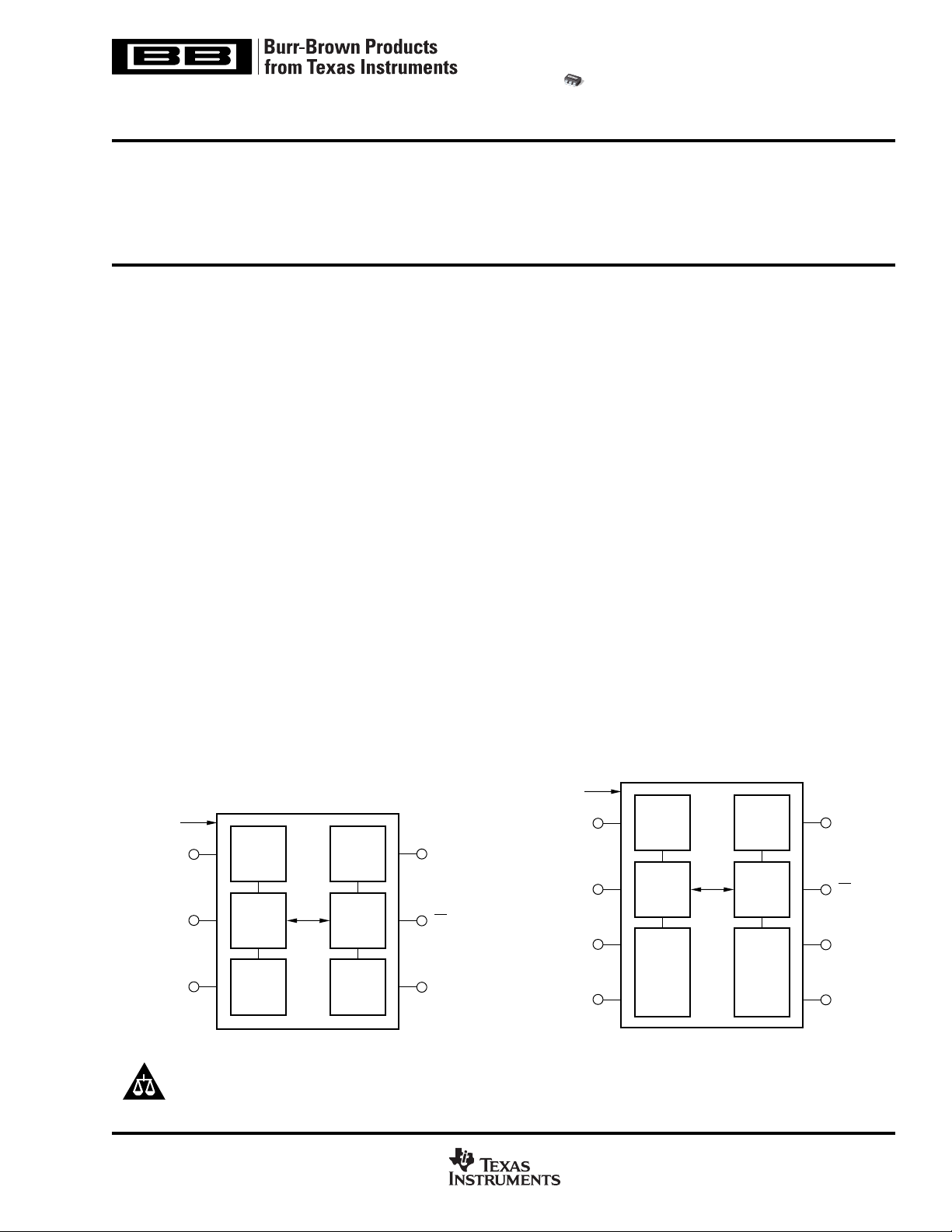
Temperature
Temperature
Diode
1
2
3
Temp.
Sensor
∆Σ
A/D
Converter
OSC
TMP122
ALERT
GND
V+
Please be aware that an important notice concerning availability, standard warranty, and use in critical applications of
Texas Instruments semiconductor products and disclaimers thereto appears at the end of this data sheet.
SPI is a registered trademark of Motorola. All other trademarks are the property of their respective owners.
PRODUCTION DATA information is current as of publication date.
Products conform to specifications per the terms of Texas Instruments
standard warranty. Production processing does not necessarily include
testing of all parameters.
Control
Logic
Serial
Interface
Config
and T emp
Register
6
SO/I
5
CS
4
SCK
www.ti.com
SO/I
SCK
NC
GND
Diode
1
Temp.
Sensor
∆Σ
2
A/D
Converter
3
OSC
45
Copyright © 2003, Texas Instruments Incorporated
TMP124
Control
Logic
Serial
Interface
Config
and T emp
Register
8
V+
7
CS
6
NC
ALERT
Page 2
ABSOLUTE MAXIMUM RATINGS
SI/O
SC
NC
GND
V+
CS
NC
ALERT
1
2
3
4
8
7
6
5
T124
TMP124
Power Supply, V+ .................................................................................. 7V
Input Voltage
Input Current ..................................................................................... 10mA
Operating Temperature Range ......................................–55°C to +150°C
Storage Temperature Range ......................................... –60°C to +150°C
Junction Temperature (T
Lead Temperature (soldering)....................................................... +300°C
(2)
....................................................................... –0.3V to 7V
Max) .................................................... +150°C
J
(1)
ELECTROSTATIC
DISCHARGE SENSITIVITY
This integrated circuit can be damaged by ESD. Texas Instruments recommends that all integrated circuits be handled with
appropriate precautions. Failure to observe proper handling
and installation procedures can cause damage.
NOTES: (1) Stresses above those listed under “Absolute Maximum Ratings”
may cause permanent damage to the device. Exposure to absolute maximum
conditions for extended periods may affect device reliability. (2) Input voltage
rating applies to all TMP122 and TMP124 input voltages.
ESD damage can range from subtle performance degradation
to complete device failure. Precision integrated circuits may be
more susceptible to damage because very small parametric
changes could cause the device not to meet its published
specifications.
PACKAGE/ORDERING INFORMATION
PRODUCT PACKAGE-LEAD DESIGNATOR
PACKAGE TEMPERATURE PACKAGE ORDERING TRANSPORT
TMP122 SOT23-6 DBV –40°C to +125°C T122 TMP122AIDBVT Tape and Reel, 250
(1)
"" "" "TMP122AIDBVR Tape and Reel, 3000
TMP124 SO-8 D –40°C to +125°C T124 TMP124AID Rails, 100
"" "" "TMP124AIDR Tape and Reel, 2500
NOTE: (1) For the most current specifications and package information, refer to our web site at www.ti.com.
SPECIFIED
RANGE MARKING NUMBER MEDIA, QUANTITY
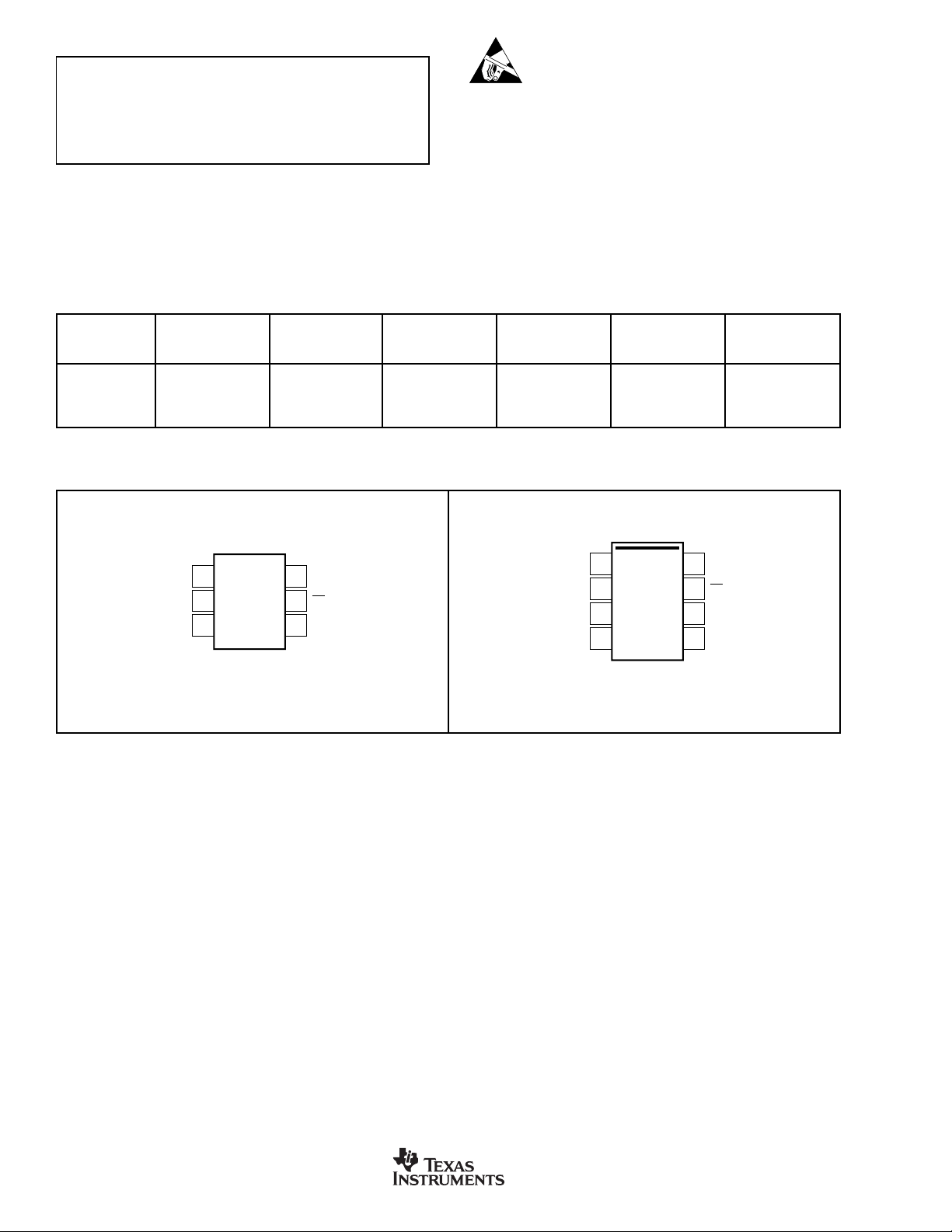
PIN CONFIGURATIONS
Top View SOT23-6
T122
ALERT
GND
V+
1
2
3
TMP122
6
SO/I
5
CS
4
SCK
Top View SO-8
NC = No Connection
2
www.ti.com
TMP122, TMP124
SBOS272B
Page 3

ELECTRICAL CHARACTERISTICS
At TA = –40°C to +125°C, and V+ = 2.7V to 5.5V, unless otherwise noted.
TMP122, TMP124
PARAMETER CONDITION MIN TYP MAX UNITS
TEMPERATURE INPUT
Range –40 +125 °C
Accuracy (Temperature Error) –25°C to +85°C ±0.5 ±1.5 °C
vs Supply –0.3 0.1 +0.3 °C/V
Resolution
(1)
DIGITAL INPUT/OUTPUT
Input Logic Levels:
V
IH
V
IL
Input Current, SO/I, SCK, CS 0V ≤ V
Output Logic Levels:
V
SO/I I
OL
V
SO/I I
OH
V
ALERT I
OL
Leakage Current ALERT 0V ≤ V
Input Capacitance, SO/I, SCK, CS, ALERT 2.5 pF
Resolution Selectable 9 to 12 + Sign Bits
Conversion Time 9-Bit + Sign 30 40 ms
POWER SUPPLY
Operating Range 2.7 5.5 V
Quiescent Current I
Shutdown Current I
Q
SD
TEMPERATURE RANGE
Specified Range –40 +125 °C
Operating Range –55 +150 °C
Storage Range –60 +150 °C
Thermal Resistance,
θ
JA
NOTE: (1) Specified for 12-bit resolution.
–40°C to +125°C ±1.0 ±2.0 °C
–55°C to +150°C ±1.5 °C
Selectable ±0.0625 °C
0.7(V+) V
0.3(V+) V
≤ V+ ±1 µA
IN
= 3mA 0.4 V
SINK
= 2mA (V+)–0.4 V
SOURCE
= 4mA 0.4 V
SINK
≤ 6V ±1 µA
IN
10-Bit + Sign 60 80 ms
11-Bit + Sign 120 160 ms
12-Bit + Sign 240 320 ms
Serial Bus Inactive 50 75 µA
Serial Bus Inactive 0.1 1 µA
SOT23-6 Surface-Mount 200 °C/W
SO-8 Surface-Mount 150 °C/W
TMP122, TMP124
SBOS272B
www.ti.com
3
Page 4
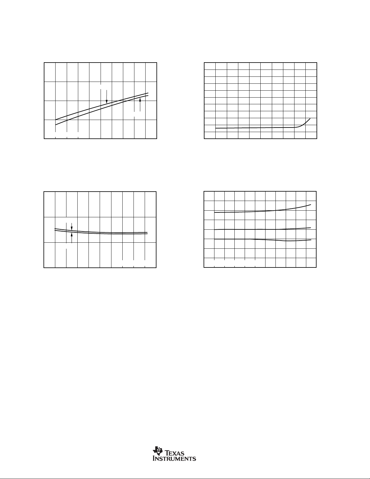
TYPICAL CHARACTERISTICS
At TA = +25°C, and V+ = 5.0V, unless otherwise noted.
70
60
50
(µA)
Q
I
40
30
400
300
200
Conversion Time (ms)
100
QUIESCENT CURRENT vs TEMPERATURE
V+ = 5V
V+ = 2.7V
Serial Bus Inactive
–60 –40 –20 0 20 40 60 80 100 120 140
Temperature (°C)
CONVERSION TIME vs TEMPERATURE
V+ = 5V
V+ = 2.7V
12-bit resolution.
–60 –40 –20 0 20 40 60 80 100 120 140
Temperature (°C)
1.0
0.9
0.8
0.7
0.6
0.5
(µA)
0.4
SD
I
0.3
0.2
0.1
0.0
–0.1
2.0
1.5
1.0
0.5
0.0
–0.5
–1.0
Temperature Error (°C)
–1.5
–2.0
SHUTDOWN CURRENT vs TEMPERATURE
–60 –40 –20 0 20 40 60 80 100 120 140
Temperature (°C)
TEMPERATURE ACCURACY vs TEMPERATURE
3 typical units 12-bit resolution.
–60 –40 –20 0 20 40 60 80 100 120 160140
Temperature (°C)
4
www.ti.com
TMP122, TMP124
SBOS272B
Page 5
APPLICATIONS INFORMATION
The TMP122 and TMP124 digital temperature sensors are
optimal for thermal management and thermal protection applications. The TMP122/TMP124 are SPI interface-compatible
and specified for a temperature range of –40°C to +125°C.
The TMP122/TMP124 require minimal external components
for operation, needing only a pull-up resistor on the ALERT
pin and a bypass capacitor on the supply. Bypass capacitors
of 0.1µF is recommended. Figure 1 shows typical connections for the TMP122 and TMP124.
V+
0.1µF
3
1
SCK
SO/I
4
6
TMP122
2
GND
ALERT
(Output)
5
CS
NOTE: Alert requires
pull-up resistor (open drain).
NC indicates pin should be left
open or floating.
SO/I
SCK
NC
FIGURE 1. Typical Connections of the TMP122 and TMP124.
To maintain accuracy in applications requiring air or surface
temperature measurement, care should be taken to isolate
the package and leads from ambient air temperature.
CS
SO/I
16-Bit
READ
16-Bit
READ
COMMAND
16-Bit
Response
FIGURE 2.Multiple Command Sequence.
1
2
TMP124
3
16-Bit
WRITE/
Embedded
Address
V+
GND
7
6
5
16-Bit
READ
0.1µF
CS
NC
ALERT
(Output)
8
4
COMMUNICATING WITH THE TMP122
The TMP122/TMP124 converts continuously. If CS is brought
low during a conversion the conversion process continues, but
the last completed conversion is available at the output register. Communication with the TMP122/TMP124 is initiated by
pulling
CS
low. The first 16 clocks of data transfer will return
temperature data from the temperature sensors. The 16-bit
data word is clocked out sign bit first, followed by the MSB. Any
portion of the 16-bit word may be read before raising
user wishes to continue with
CS
low, the following 16 clocks
transfer in a READ or WRITE command. READ and WRITE
commands are described in Tables I and II.
The READ command contains an embedded address in bits
D4 and D3 to identify which register to read. Bits D4 and D3
are internally registered and will hold their value following a
READ command until a entire 16-bit read is completed by the
user. The completion of the 16-bit READ acknowledges that
the READ command has been completed. If the user issues
a READ command and then raises
CS
with less than 16
subsequent clocks, the data from that register will be available
at the next fall of
CS
. The registered READ address will
remain in effect until a full 16 clocks have been received. After
the completion of a 16-bit READ from the part, the READ
address is reset to return data from the Temperature Register.
A WRITE command to a register will not change the READ
address registered. For further discussion on the READ address register, see the
Read Address Register
Multiple commands may be strung together as illustrated in
Figure 2. The TMP122/TMP124 accepts commands alternating with 16-bit response data. On lowering
always responds with a READ from the address location
indicated by the READ address register. If the next command is a READ command then data is returned from the
address specified by the READ command with the 16th clock
resetting the READ address register to the default temperature register. The TMP122/TMP124 then expect a 16-bit
command. If the command is a WRITE command, then the
16 clocks following the command will again return temperature data.
Figures 3, 4, 5, and 6 detail the communication sequences.
CS
section.
CS
, the part
. If the
Read Command D15 D14 D13 D12 D11 D10 D9 D8 D7 D6 D5 D4 D3 D2 D1 D0
Temperature 10000000000 0 0 000
Configuration Register 10000000000 0 1000
Low Temp Threshold 10000000000 1 0000
High Temp Threshold 1000000 0000 1 1 000
TABLE I. Read Command.
Write Command D15 D14 D13 D12 D11 D10 D9 D8 D7 D6 D5 D4 D3 D2 D1 D0
Configuration Register 0000D1D0R1R0F1F0POLTM1TM00 1 0
Low Temp Threshold T12 T11 T10 T9 T8 T7 T6 T5 T4 T3 T2 T1 T0 1 0 0
High Temp Threshold T12 T11 T10 T9 T8 T7 T6 T5 T4 T3 T2 T1 T0 1 1 0
Shutdown Command xxxxxxxx11111 1 1 1
TABLE II. Write Command.
TMP122, TMP124
SBOS272B
www.ti.com
5
Page 6
SO/I
SCK
SO/I
CS
SCK
CS
...
ZZ1D3D4D5D6D7D8D9D10D11D12D13D14D15
CS
16-Bit
READ
(Continued)
16-Bit
WRITE/
Embedded
Address
...
SO/I
FIGURE 3. READ followed by WRITE COMMAND to T
CS
SCK
SO/I
CS
SCK
SO/I
SO/I
CS
16-Bit
READ
(Continued)
16-Bit
WRITE/
Embedded
Address
...
LOW/THIGH
Register.
FIGURE 4. READ followed by WRITE COMMAND to Configuration Register.
CS
SCK
SO/I
SO/I
CS
16-Bit
READ
16-Bit
READ
COMMAND
16-Bit
Response
NOTE: (1) 0 indicates T
register, 1 indicates T
LOW
(1)
HIGH
00/1
register.
1T0T1T2T3T4T5T6T7T8T9T10T11T12
...
ZZ1D3D4D5D6D7D8D9D10D11D12D13D14D15
010TM0TM1POLF0F1R0R1D0D10000
...
ZZ1D3D4D5D6D7D8D9D10D11D12D13D14D15
(Continued)
(Continued)
...
...
CS
SCK
SO/I
CS
SCK
SO/I
FIGURE 5. READ followed by READ COMMAND and Response.
CS
SO/I
16-Bit
READ
CS
SCK
SO/I
FIGURE 6. Data READ.
...
000P0P100000000001
ZZ1D3D4D5D6D7D8D9D10D11D12D13D14D15
ZZ1D3D4D5D6D7D8D9D10D11D12D13D14D15
6
www.ti.com
TMP122, TMP124
SBOS272B
Page 7

READ ADDRESS REGISTER
Figure 7 shows the internal register structure of the
TMP122/TMP124. Table III describes the addresses of the
registers available. The READ address register uses the two
bits to identify which of the data registers should respond to
a read command. Following a complete 16-bit read, the
READ address register is reset to the default power-up state
of P1/P0 equal 0/0.
READ Address
Register
Temperature
Register
Configuration
Register
T
LOW
Register
T
HIGH
Register
I/O
Control
Interface
CS
SCK
SO/I
FIGURE 7. Internal Register Structure of the TMP122 and
TMP124.
P1 P0 REGISTER
0 0 Temperature Register (READ Only)
0 1 Configuration Register (READ/WRITE)
10T
11T
Register (READ/WRITE)
LOW
Register (READ/WRITE)
HIGH
TABLE III. Pointer Addresses of the TMP122 and TMP124
Registers.
TEMPERATURE REGISTER
The Temperature Register of the TMP122/TMP124 is a 16bit, signed read-only register that stores the output of the
most recent conversion. The TMP122/TMP124 are specified for the temperature range of –40°C to +125°C with
operation from –55°C to +150°C. Up to 16 bits can be read
to obtain data and are described in Table IV. The first 13 bits
are used to indicate temperature where bit D2 is 1, and D1,
D0 are in a high impedance state. Data format for temperature is summarized in Table V. Following power-up or reset,
the Temperature Register will read 0°C until the first conversion is complete.
D15 D14 D13 D12 D11 D10 D9 D8
T12 T11 T10 T9 T8 T7 T6 T5
D7 D6 D5 D4 D3 D2 D1 D0
T4 T3 T2 T1 T0 1 Z Z
TABLE IV. Temperature Register.
TEMPERATURE DIGITAL OUTPUT
(°C) (BINARY) HEX
150 0100 1011 0000 0111 4B07
125 0011 1110 1000 0111 3E87
25 0000 1100 1000 0111 0C87
0.0625 0000 0000 0000 1111 000F
0 0000 0000 0000 0111 0007
–0.0625 1111 1111 1111 1111 FFFF
–25 1111 0011 1000 0111 F387
–55 1110 0100 1000 0111 E487
NOTE: (1) The last 2 bits are high impedance and are shown as 11 in the table.
(1)
TABLE V. Temperature Data Format.
The user can obtain 9, 10, 11, or 12 bits of resolution by
addressing the Configuration Register and setting the resolution bits accordingly.
For 9-, 10-, or 11-bit resolution, the most
significant bits in the Temperature Register are used with the
unused LSBs set to zero.
CONFIGURATION REGISTER
The Configuration Register is a 16-bit read/write register
used to store bits that control the operational modes of the
temperature sensor. Read/write operations are performed
MSB first. The format of the Configuration Register for the
TMP122/TMP124 is shown in Table VI, followed by a breakdown of the register bits. The power-up/reset value of the
Configuration Register bits R1/R0 equal 1/1, all other bits
equal zero.
D15 D14 D13 D12 D11 D10 D9 D8
0 0 0 0 D1 D0 R1 R0
D7 D6 D5 D4 D3 D2 D1 D0
F1 F0 POL TM1 TM0 0 1 0
TABLE VI. Configuration Register.
SHUTDOWN MODE (SD)
The Shutdown Mode of the TMP122/TMP124 can be used to
shut down all device circuitry except the serial interface.
Shutdown mode occurs when the last 8 bits of the WRITE
command are equal to 1, and will occur once the current
conversion is completed, reducing current consumption to
less than 1µA. To take the part out of shutdown, send any
command or pattern after the 16-bit read with the last 8 bits
not equal to one. Power on default is in active mode.
TMP122, TMP124
SBOS272B
www.ti.com
7
Page 8

THERMOSTAT MODE (TM1/TM0)
The Thermostat Mode bits of the TMP122/TMP124 indicate to
the device whether to operate in Comparator Mode, Interrupt
Mode or Interrupt Comparator Mode. For more information on
Comparator and Interrupt Mode, see text HIGH and LOW limit
registers. The bit assignments for thermostat mode are
described in Table VII. Power on default is comparator mode.
TM1 TM0 MODE OF OPERATION
0 0 Comparator Mode
0 1 Interrupt Mode
1 0 Interrupt Comparator Mode
11 —
TABLE VII. Mode Settings of the TMP122.
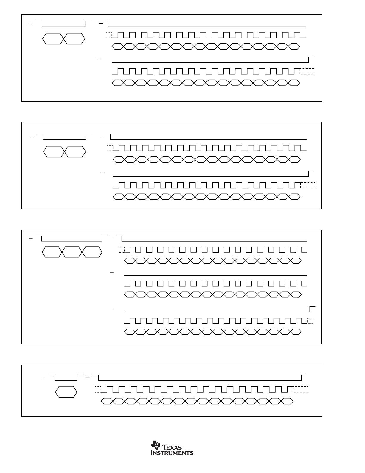
POLARITY (POL)
The Polarity Bit of the TMP122/TMP124 adjusts the polarity
of the ALERT pin output. By default, POL = 0 and the ALERT
pin will be active LOW, as shown in Figure 8. For POL = 1
the ALERT Pin will be active HIGH, and the state of the
ALERT Pin is inverted.
T
Read
T
HIGH
LOW
Measured
Temperature
TMP122/124 ALERT PIN
(Comparator Mode)
POL = 0
TMP122/124 ALERT PIN
(Interrupt Mode)
POL = 0
TMP122/124 ALERT PIN
(Interrupt/Comparator Mode)
POL = 0
Read Read
Time
HIGH AND LOW LIMIT REGISTERS
In Comparator Mode (TM1/TM0 = 0/0), the ALERT Pin of the
TMP122/TMP124 becomes active when the temperature
equals or exceeds the value in T
consecutive number of faults according to fault bits F1 and
F0. The ALERT pin will remain active until the temperature
falls below the indicated T
value for the same number of
LOW
faults.
In Interrupt Mode (TM1/TM0 = 0/1) the ALERT pin becomes
active when the temperature equals or exceeds T
consecutive number of fault conditions. The ALERT pin
remains active until a read operation of any register occurs.
The ALERT pin will also be cleared if the device is placed in
Shutdown Mode. Once the ALERT pin is cleared, it will only
become active again by the temperature falling below T
When the temperature falls below T
becomes active and remains active until cleared by a read
operation of any register. Once the ALERT pin is cleared, the
above cycle will repeat with the ALERT pin becoming active
when the temperature equals or exceeds T
In Interrupt/Comparator Mode (TM1/TM0 = 1/0), the ALERT
Pin of the TMP122/TMP124 becomes active when the temperature equals or exceeds the value in T
a consecutive number of faults according to fault bits F1 and
F0. The ALERT pin will remain active until the temperature
falls below the indicated T
value for the same number of
LOW
faults and a communication with the device has occurred
after that point.
Operational modes are represented in Figure 8. Tables IX
and X describe the format for the T
Power-up reset values for T
and T
= 75°C. The format of the data for T
LOW
HIGH
and T
is the same as for the Temperature Register.
All 13 bits for the Temperature, T
HIGH
used in the comparisons for the ALERT function for all converter resolutions. The three LSBs in T
affect the ALERT output even if the converter is configured for
9-bit resolution.
and generates a
HIGH
, the ALERT pin
LOW
HIGH
and generates
HIGH
and T
HIGH
LOW
, and T
are: T
LOW
HIGH
and T
LOW
HIGH
registers are
HIGH
.
registers.
= 80°C
HIGH
and T
LOW
for a
LOW
LOW
can
.
FIGURE 8. ALERT Output Transfer Function Diagrams.
FAULT QUEUE (F1/F0)
A fault condition occurs when the measured temperature
exceeds the limits set in the T
HIGH
and T
Fault Queue is provided to prevent a false alert due to
environmental noise and requires consecutive fault measurements to trigger the alert function of the TMP122/TMP124.
Table VIII defines the number of consecutive faults required
to trigger a consecutive alert condition. Power-on default for
F1/F0 is 0/0.
F1 F0 CONSECUTIVE FAULTS
00 1
01 2
10 4
11 6
TABLE VIII. Fault Settings of the TMP122 and TMP124.
8
registers. The
LOW
www.ti.com
D15 D14 D13 D12 D11 D10 D9 D8
H12 H11 H10 H9 H8 H7 H6 H5
D7 D6 D5 D4 D3 D2 D1 D0
H4 H3 H2 H1 H0 1 1 0
TABLE IX. T
D15 D14 D13 D12 D11 D10 D9 D8
L12 L11 L10 L9 L8 L7 L6 L5
D7 D6 D5 D4 D3 D2 D1 D0
L4 L3 L2 L1 L0 1 0 0
TABLE X. T
HIGH
Register.
LOW
Register.
TMP122, TMP124
SBOS272B
Page 9

CONVERTER RESOLUTION (R1/R0)
The Converter Resolution Bits control the resolution of the
internal Analog-to-Digital (A/D) converter. This allows the user
to maximize efficiency by programming for higher resolution or
faster conversion time. Table XI identifies the Resolution Bits
and the relationship between resolution and conversion time.
The TMP122/TMP124 have a default resolution of 12 bits.
D1 D0 CONVERSION TIME CONVERSION PERIOD
0 0 0.25s 0.25s
0 1 0.25s 0.5s
1 0 0.25s 1s
1 1 0.25s 8s
TABLE XII. Conversion Delay for 12-Bit Resolution.
R1 R0 RESOLUTION (typical)
0 0 9 Bits (0.5°C) plus sign 30ms
0 1 10 Bits (0.25°C) plus sign 60ms
1 0 11 Bits (0.125°C) plus sign 120ms
1 1 12 Bits (0.0625°C) plus sign 240ms
TABLE XI. Resolution of the TMP122 and TMP124.
DELAY TIME
The Delay Bits control the amount of time delay between each
CONVERSION TIME
D1/D0 = 0/1
0.25s
0.25s
D1/D0 = 1/0
0.25s
D1/D0 = 1/1
12-Bit Resolution
0.5s
1s
8s
conversion. This feature allows the user to maximize power
savings by eliminating unnecessary conversions, and minimizing current consumption. During active conversion the TMP122/
TMP124 typically requires 50µA of current for approximately
FIGURE 9. Conversion Time and Period Description.
0.25s conversion time, and approximately 20µA for idle times
between conversions. Delay settings are identified in Table XII
as conversion time and period, and are shown in Figure 9.
Default power up is D1/D0 equal 0/0. Conversion time and
conversion periods scale with resolution. Conversion period
Timing Diagrams
The TMP122/TMP124 are SPI compatible. Figures 10 to 12
describe the various timing parameters of the TMP122/
TMP124 with timing definitions in Table XIII.
denotes time between conversion starts.
PARAMETER MIN MAX UNITS
SCK Period t
Data In to Rising Edge SCK Setup Time t
SCK Falling Edge to Output Data Delay t
SCK Rising Edge to Input Data Hold Time t
CS to Rising Edge SCK Set-Up Time t
CS to Output Data Delay t
CS Rising Edge to Output High Impedance t
1
2
3
4
5
6
7
100 ns
20 ns
30 ns
20 ns
40 ns
30 ns
30 ns
TABLE XIII. Timing Description.
50µA (active)
20µA (idle)
TMP122, TMP124
SBOS272B
www.ti.com
9
Page 10

SCK
t
5
t
CS
t
6
SO/I
FIGURE 10. Output Data Timing Diagram.
SCK
CS
SO/I
FIGURE 11. High Impedance Output Timing Diagram.
1
t
3
SCK
CS
t
SO/I
t
7
7
SCK
t
4
CS
SO/I
FIGURE 12. Input Data Timing Diagram.
SCK
t
2
t
4
t
2
CS
SO/I
10
www.ti.com
TMP122, TMP124
SBOS272B
Page 11
PACKAGE OPTION ADDENDUM
www.ti.com
10-Jun-2014
PACKAGING INFORMATION
Orderable Device Status
TMP122AIDBVR ACTIVE SOT-23 DBV 6 3000 Green (RoHS
TMP122AIDBVRG4 ACTIVE SOT-23 DBV 6 3000 Green (RoHS
TMP122AIDBVT ACTIVE SOT-23 DBV 6 250 Green (RoHS
TMP122AIDBVTG4 ACTIVE SOT-23 DBV 6 250 Green (RoHS
TMP124AID ACTIVE SOIC D 8 75 Green (RoHS
TMP124AIDG4 ACTIVE SOIC D 8 75 Green (RoHS
TMP124AIDR ACTIVE SOIC D 8 2500 Green (RoHS
(1)
The marketing status values are defined as follows:
ACTIVE: Product device recommended for new designs.
LIFEBUY: TI has announced that the device will be discontinued, and a lifetime-buy period is in effect.
NRND: Not recommended for new designs. Device is in production to support existing customers, but TI does not recommend using this part in a new design.
PREVIEW: Device has been announced but is not in production. Samples may or may not be available.
OBSOLETE: TI has discontinued the production of the device.
Package Type Package
(1)
Drawing
Pins Package
Qty
Eco Plan
(2)
& no Sb/Br)
& no Sb/Br)
& no Sb/Br)
& no Sb/Br)
& no Sb/Br)
& no Sb/Br)
& no Sb/Br)
Lead/Ball Finish
(6)
CU NIPDAU Level-2-260C-1 YEAR -40 to 125 T122
CU NIPDAU Level-2-260C-1 YEAR -40 to 125 T122
CU NIPDAU Level-2-260C-1 YEAR -40 to 125 T122
CU NIPDAU Level-2-260C-1 YEAR -40 to 125 T122
CU NIPDAU Level-1-260C-UNLIM -55 to 125 T124
CU NIPDAU Level-1-260C-UNLIM -55 to 125 T124
CU NIPDAU Level-1-260C-UNLIM -55 to 125 T124
MSL Peak Temp
(3)
Op Temp (°C) Device Marking
(4/5)
(2)
Eco Plan - The planned eco-friendly classification: Pb-Free (RoHS), Pb-Free (RoHS Exempt), or Green (RoHS & no Sb/Br) - please check http://www.ti.com/productcontent for the latest availability
information and additional product content details.
TBD: The Pb-Free/Green conversion plan has not been defined.
Pb-Free (RoHS): TI's terms "Lead-Free" or "Pb-Free" mean semiconductor products that are compatible with the current RoHS requirements for all 6 substances, including the requirement that
lead not exceed 0.1% by weight in homogeneous materials. Where designed to be soldered at high temperatures, TI Pb-Free products are suitable for use in specified lead-free processes.
Pb-Free (RoHS Exempt): This component has a RoHS exemption for either 1) lead-based flip-chip solder bumps used between the die and package, or 2) lead-based die adhesive used between
the die and leadframe. The component is otherwise considered Pb-Free (RoHS compatible) as defined above.
Green (RoHS & no Sb/Br): TI defines "Green" to mean Pb-Free (RoHS compatible), and free of Bromine (Br) and Antimony (Sb) based flame retardants (Br or Sb do not exceed 0.1% by weight
in homogeneous material)
(3)
MSL, Peak Temp. - The Moisture Sensitivity Level rating according to the JEDEC industry standard classifications, and peak solder temperature.
(4)
There may be additional marking, which relates to the logo, the lot trace code information, or the environmental category on the device.
Samples
Addendum-Page 1
Page 12

PACKAGE OPTION ADDENDUM
www.ti.com
(5)
Multiple Device Markings will be inside parentheses. Only one Device Marking contained in parentheses and separated by a "~" will appear on a device. If a line is indented then it is a continuation
of the previous line and the two combined represent the entire Device Marking for that device.
10-Jun-2014
(6)
Lead/Ball Finish - Orderable Devices may have multiple material finish options. Finish options are separated by a vertical ruled line. Lead/Ball Finish values may wrap to two lines if the finish
value exceeds the maximum column width.
Important Information and Disclaimer:The information provided on this page represents TI's knowledge and belief as of the date that it is provided. TI bases its knowledge and belief on information
provided by third parties, and makes no representation or warranty as to the accuracy of such information. Efforts are underway to better integrate information from third parties. TI has taken and
continues to take reasonable steps to provide representative and accurate information but may not have conducted destructive testing or chemical analysis on incoming materials and chemicals.
TI and TI suppliers consider certain information to be proprietary, and thus CAS numbers and other limited information may not be available for release.
In no event shall TI's liability arising out of such information exceed the total purchase price of the TI part(s) at issue in this document sold by TI to Customer on an annual basis.
OTHER QUALIFIED VERSIONS OF TMP122 :
Enhanced Product: TMP122-EP
•
NOTE: Qualified Version Definitions:
Enhanced Product - Supports Defense, Aerospace and Medical Applications
•
Addendum-Page 2
Page 13

PACKAGE MATERIALS INFORMATION
www.ti.com 8-Jul-2011
TAPE AND REEL INFORMATION
*All dimensions are nominal
Device Package
Type
TMP122AIDBVR SOT-23 DBV 6 3000 178.0 9.0 3.23 3.17 1.37 4.0 8.0 Q3
TMP122AIDBVT SOT-23 DBV 6 250 178.0 9.0 3.23 3.17 1.37 4.0 8.0 Q3
Package
Drawing
Pins SPQ Reel
Diameter
(mm)
Reel
Width
W1 (mm)
A0
(mm)B0(mm)K0(mm)P1(mm)W(mm)
Pin1
Quadrant
Pack Materials-Page 1
Page 14

PACKAGE MATERIALS INFORMATION
www.ti.com 8-Jul-2011
*All dimensions are nominal
Device Package Type Package Drawing Pins SPQ Length (mm) Width (mm) Height (mm)
TMP122AIDBVR SOT-23 DBV 6 3000 180.0 180.0 18.0
TMP122AIDBVT SOT-23 DBV 6 250 180.0 180.0 18.0
Pack Materials-Page 2
Page 15
Page 16

Page 17

Page 18

Page 19

IMPORTANT NOTICE
Texas Instruments Incorporated and its subsidiaries (TI) reserve the right to make corrections, enhancements, improvements and other
changes to its semiconductor products and services per JESD46, latest issue, and to discontinue any product or service per JESD48, latest
issue. Buyers should obtain the latest relevant information before placing orders and should verify that such information is current and
complete. All semiconductor products (also referred to herein as “components”) are sold subject to TI’s terms and conditions of sale
supplied at the time of order acknowledgment.
TI warrants performance of its components to the specifications applicable at the time of sale, in accordance with the warranty in TI’s terms
and conditions of sale of semiconductor products. Testing and other quality control techniques are used to the extent TI deems necessary
to support this warranty. Except where mandated by applicable law, testing of all parameters of each component is not necessarily
performed.
TI assumes no liability for applications assistance or the design of Buyers’ products. Buyers are responsible for their products and
applications using TI components. To minimize the risks associated with Buyers’ products and applications, Buyers should provide
adequate design and operating safeguards.
TI does not warrant or represent that any license, either express or implied, is granted under any patent right, copyright, mask work right, or
other intellectual property right relating to any combination, machine, or process in which TI components or services are used. Information
published by TI regarding third-party products or services does not constitute a license to use such products or services or a warranty or
endorsement thereof. Use of such information may require a license from a third party under the patents or other intellectual property of the
third party, or a license from TI under the patents or other intellectual property of TI.
Reproduction of significant portions of TI information in TI data books or data sheets is permissible only if reproduction is without alteration
and is accompanied by all associated warranties, conditions, limitations, and notices. TI is not responsible or liable for such altered
documentation. Information of third parties may be subject to additional restrictions.
Resale of TI components or services with statements different from or beyond the parameters stated by TI for that component or service
voids all express and any implied warranties for the associated TI component or service and is an unfair and deceptive business practice.
TI is not responsible or liable for any such statements.
Buyer acknowledges and agrees that it is solely responsible for compliance with all legal, regulatory and safety-related requirements
concerning its products, and any use of TI components in its applications, notwithstanding any applications-related information or support
that may be provided by TI. Buyer represents and agrees that it has all the necessary expertise to create and implement safeguards which
anticipate dangerous consequences of failures, monitor failures and their consequences, lessen the likelihood of failures that might cause
harm and take appropriate remedial actions. Buyer will fully indemnify TI and its representatives against any damages arising out of the use
of any TI components in safety-critical applications.
In some cases, TI components may be promoted specifically to facilitate safety-related applications. With such components, TI’s goal is to
help enable customers to design and create their own end-product solutions that meet applicable functional safety standards and
requirements. Nonetheless, such components are subject to these terms.
No TI components are authorized for use in FDA Class III (or similar life-critical medical equipment) unless authorized officers of the parties
have executed a special agreement specifically governing such use.
Only those TI components which TI has specifically designated as military grade or “enhanced plastic” are designed and intended for use in
military/aerospace applications or environments. Buyer acknowledges and agrees that any military or aerospace use of TI components
which have not been so designated is solely at the Buyer's risk, and that Buyer is solely responsible for compliance with all legal and
regulatory requirements in connection with such use.
TI has specifically designated certain components as meeting ISO/TS16949 requirements, mainly for automotive use. In any case of use of
non-designated products, TI will not be responsible for any failure to meet ISO/TS16949.
Products Applications
Audio www.ti.com/audio Automotive and Transportation www.ti.com/automotive
Amplifiers amplifier.ti.com Communications and Telecom www.ti.com/communications
Data Converters dataconverter.ti.com Computers and Peripherals www.ti.com/computers
DLP® Products www.dlp.com Consumer Electronics www.ti.com/consumer-apps
DSP dsp.ti.com Energy and Lighting www.ti.com/energy
Clocks and Timers www.ti.com/clocks Industrial www.ti.com/industrial
Interface interface.ti.com Medical www.ti.com/medical
Logic logic.ti.com Security www.ti.com/security
Power Mgmt power.ti.com Space, Avionics and Defense www.ti.com/space-avionics-defense
Microcontrollers microcontroller.ti.com Video and Imaging www.ti.com/video
RFID www.ti-rfid.com
OMAP Applications Processors www.ti.com/omap TI E2E Community e2e.ti.com
Wireless Connectivity www.ti.com/wirelessconnectivity
Mailing Address: Texas Instruments, Post Office Box 655303, Dallas, Texas 75265
Copyright © 2015, Texas Instruments Incorporated
Page 20

 Loading...