

Page 1
User's Guide
SNOU160–April 2018
TMP116METER-EVM User's Guide
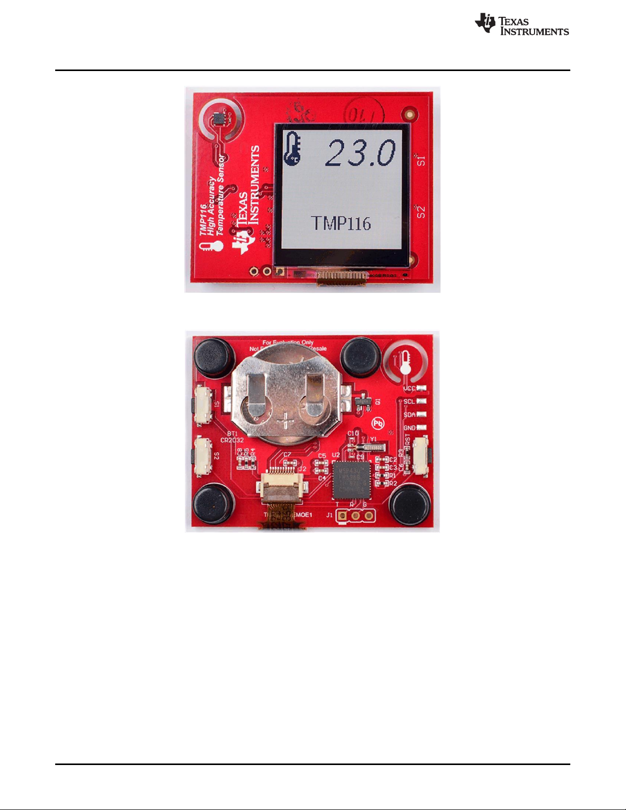
The TMP116METER-EVM provides the user with an easy-to-read LCD screen while using the TMP116 for
measurement of ambient air temperature. The EVM measures 1.83 in × 1.45 in, so the system is fitted to
a small form factor for further convenience in space-constrained environments. The onboard
microcontroller (MCU) communicates with the temperature sensor using I2C communication protocol and
displays the measurement onto an LCD through SPI protocol.
Contents
1 Introduction ................................................................................................................... 1
2 Setup and Test Results ..................................................................................................... 4
3 Schematic and Bill of Materials ............................................................................................ 6
List of Figures
1 TMP116METER-EVM Front View ........................................................................................ 2
2 TMP116METER-EVM Back View ......................................................................................... 2
3 Software Flow Chart ........................................................................................................ 5
4 System Current Consumption.............................................................................................. 6
5 TMP116METER-EVM Schematic ......................................................................................... 7
Trademarks
All trademarks are the property of their respective owners.
1 Introduction
The TMP116METER-EVM comes pre-loaded with firmware that ensures successful operation upon
connection of the coin cell battery. Because the MCU is flashed using JTAG protocol, the test, reset, and
ground pins are broken out to a three-pin header for the user to have the option to flash the
MSP430FR5969 MCU. The device features three push-buttons: Button S1 functions to perform RESET,
S2 switches the temperature display format on the display (Celsius or Fahrenheit), and another button
(S3) can be programmed by the user. Test points are provided for the user to probe the clock and data
signal lines corresponding to I2C data transfer in addition to power and ground probe locations.
SNOU160–April 2018
Submit Documentation Feedback
Copyright © 2018, Texas Instruments Incorporated
TMP116METER-EVM User's Guide
1
Page 2
Introduction
www.ti.com
Figure 1. TMP116METER-EVM Front View
1.1 Features
Low-power, high-accuracy temperature sensor: The TMP116 offers 16-bit resolution with an accuracy of
±0.2ºC (from -10ºC to +85ºC).
Ultra-low-power MCU: The MSP430FR5969 can operate from 1.8V to 3.6V while consuming 0.4 µA in
standby and 0.02 µA in shutdown.
Coin Cell Operation: CR2032 supplies 3V with a nominal capacity of 225 mAh
2
TMP116METER-EVM User's Guide
Figure 2. TMP116METER-EVM Back View
Copyright © 2018, Texas Instruments Incorporated
Submit Documentation Feedback
SNOU160–April 2018
Page 3
www.ti.com
1.1.1 TMP116 Temperature Sensor
The TMP116 sensor measures the ambient air temperature with high precision and low power
consumption. This device provides a 16-bit temperature result with a resolution of 0.0078°C without
calibration. The TMP116 units are 100% tested on a production setup that is NIST traceable and verified
with equipment calibrated to ISO and IEC 17025 accredited standards. The sensor comes in a WSON
(2.00 mm × 2.00 mm) package and consumes minimal current that, in addition to providing power savings,
minimizes self-heating and improves measurement accuracy. The TMP116 operates from 1.9 V to 5.5 V
and typically consumes 3.5 µA.
1.1.2 MSP430FR5969 Mixed-Signal Microcontroller
The MSP430FR5969 is an ultra-low-power MCU that is optimized for lowered energy budgets in end
equipment.
The device is a member of the MSP430FR59xx family of ultra-low-power mixed-signal MCUs featuring
generous FRAM capabilities to enhance low-power designs in addition to intelligent peripherals to allow for
varied application implementation. Updating FRAM takes 100× less time than DRAM, and there is no preerase required. In addition, FRAM includes faster write speeds, unified memory, and low-energy writes.
Unified memory refers to program, data, and storage registers in one single place, which expedites the
software run. Because of its fast write speeds, FRAM has near infinite endurance. In a remote sensor,
data could be written more often for improved data accuracy, or it could collect data for longer. Due to the
lack of a charge pump, FRAM enables lower average and peak power during writes. FRAM is also
nonvolatile (that is, retains its contents upon power loss). Using the MSP430 MCU with FRAM allows for
on-the-fly writes, as opposed to buffered in RAM. The bitwise programmable memory can be used at the
programmer’s convenience for data or program storage. FRAM also offers advantages in security and is
inherently more secure due to its makeup. Also, de-layering is not effective. In comparison to MCUs with
flash, FRAM:
• Is very easy to use
• Requires no setup or preparation such as unlocking of control registers
• Is not segmented and each bit is individually erasable, writable, and addressable
• Does not require an erase before a write
• Allows low-power write accesses (does not require a charge pump)
• Can be written to across the full voltage range (1.8 V to 3.6 V)
• Can be written to at speeds close to 8MBps (maximum flash write speed including the erase time is
approximately 14 kBps)
• Does not require additional power to write to FRAM when compared to reading from FRAM
Introduction
1.2 Applications
The primary application of this EVM is to showcase a low power solution for temperature monitoring by
utilizing low power-consumption devices.
A battery voltage monitoring system allows the user to implement in firmware. A potential divider serves to
feed an ADC-enabled GPIO of the MSP430 MCU. That way, voltage sags intrinsic to battery operation
over time can be monitored and optionally displayed along with temperature measurement results;
however, this requires firmware modification. VCCMonitor is calculated as follows:
Select R4 and R5 to provide appropriate drive current to the ADC. In addition, the system features a
reverse polarity protection FET applied to the battery terminals. This FET acts as a load switch in the
system. Looking at the schematic, the body diode of Q1 sits connected between the drain and source of
Q1. The anode is connected to the drain, while the cathode is connected to the gate. When the battery is
connected correctly, the body diode is forward biased and conducts current from the drain to the source.
Because Q1 is a P-channel MOSFET, the gate voltage is brought below the source voltage, providing the
correct turnon condition. When the battery is connected in reverse, the gate of Q1 is receiving a voltage
above the source voltage. Therefore, Q1 does not turn on and current is not passed to the load through
conduction of the body diode.
SNOU160–April 2018
Submit Documentation Feedback
Copyright © 2018, Texas Instruments Incorporated
TMP116METER-EVM User's Guide
(1)
3
Page 4

Setup and Test Results
2 Setup and Test Results
2.1 Hardware
The TMP116METER-EVM requires a Panasonic CR2032 coin cell battery
which is not included.
NOTE: The TMP116METER-EVM requires a Panasonic CR2032 coin cell battery which is not included.
The TMP116METER-EVM includes:
• MSP430FR5969 MCU
• Three push-button switches
• TMP116 temperature sensor
• LSO13B7DH03 LCD
• 32-kHz FC-135 32.7680KA-A3 crystal
• Associated discrete components
• For a comprehensive list of all parts, see the Bill of Materials (BOM).
2.2 Software
This TMP116METER-EVM ships pre-loaded with software for its MSP430FR5969 MCU. When the battery
is loaded, the display shows a Texas Instruments splash screen and then proceeds to display the current
temperature and humidity. The rest of this section details the operation of the software.
Included with this reference design is a software package that contains a Code Composer Studio (CCS)
project designed for the MSP430FR5969 mCU. For proper evaluation, import the CCS project into CCS
v7.3 or later with TI Compiler v16.9.4.LTS or later.
After reset or power-on, several hardware initializations take place. All GPIO pins are configured as
outputs and driven to logic low to save power. The pins that are used are then reconfigured for their
intended purpose. The MSP430 MCU’s internal oscillator, known as DCO, is configured for 8 MHz and
connected to the internal signals SMCLK and MCLK. The external 32-kHz real-time crystal (RTC) is
connected to the low-frequency clock inputs (LFXT), so the LFXT is configured as the source of the
internal signal ACLK (Aux Clock). TIMER A is configured as a counter with ACLK as source. Conveniently,
a count of 32768 (215) is equivalent to 1 second, a count of 16384 (214) is equivalent to a half second,
and so on. The eUSCI B0 peripheral is configured for I2C communication with the TMP116 device. Finally,
the eUSCI A1 peripheral is configured for SPI use with the display, and the Sharp display is initialized.
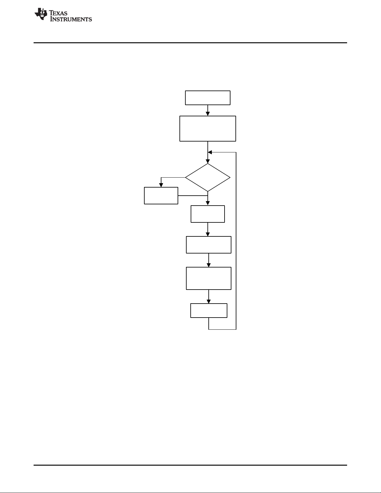
The next step in the software is to begin the loop.
On each iteration, the MSP430 MCU begins by checking the state of the button S1 and setting the Celsius
and Fahrenheit variable. An I2C Write transaction is then performed to instruct the TMP116 to begin a
temperature measurement. This measurement takes a few milliseconds (for conversion time, see
TMP116x High-Accuracy, Low-Power, Digital Temperature Sensor With SMBus- and I2C-Compatible
Interface ), so the MSP430 MCU is configured for LPM4 during the down time. After TIMER A interrupts
and resumes, the temperature data is retrieved from the TMP116. The values for temperature are
converted to characters using the tmp-decode.c library. This library is designed to provide string
conversion without loss of 16-bit precision, but it can be adjusted for less precision. Finally, the
temperature string updates the display and the MSP430 MCU returns to LPM4 for 2 seconds before
looping.
www.ti.com
CAUTION
4
TMP116METER-EVM User's Guide
Copyright © 2018, Texas Instruments Incorporated
Submit Documentation Feedback
SNOU160–April 2018
Page 5
Reset / Power Up
Toggle Celsius/
Fahrenheit
Check
S1
button
Setup MCU pins, clocks,
Timer A, I2C
Initialize Graphics Library
(GRLIB) and Sharp Display
Pressed
Trigger
Measurement
Sleep (LPM4) during
measurement
Retrieve
Temperature Result
Update Screen
Sleep (LPM4) for
2 seconds
www.ti.com
2.3 Programming
The TMP116 meter can be flashed or debugged using the Spy-By-Wire (SBW) interface. The
MSP430FR5969’s SBW interface is available at header J1 pins TEST and RST. Connect these pins, and
GND/VCC as appropriate, to an MSP430 or a standalone debugger such as MSP-FET. For more
information, see MSP Debuggers .
Setup and Test Results
2.3.1 System Current Consumption
Although the current consumption of the system in its inactive mode is clearly defined by summing each
inactive mode current specification in device data sheets, it is not so clear when the devices are active.
Therefore, this test is set up to measure the current consumption of the system in active mode. The
measurement is taken using a small series resistor connected to a simple instrumentation amplifier to
perform a differential measurement across the resistor. This arrangement is used because the standard
probes of an oscilloscope can only take single-ended measurements.
The below image yields the current consumption of the system while it is in its active mode.
Figure 3. Software Flow Chart
SNOU160–April 2018
Submit Documentation Feedback
Copyright © 2018, Texas Instruments Incorporated
TMP116METER-EVM User's Guide
5
Page 6

Schematic and Bill of Materials
www.ti.com
Figure 4. System Current Consumption
Because the gain of the instrumentation amplifier is programmed to 1000, the 1.65-V measurement
highlighted by cursor B corresponds to 1.02 mA consumed by the system. The transactions taking place
during the system’s active mode cycle are:
• MSP430 MCU wakes up due to interrupt by Timer A.
• MSP430 MCU communicates with the TMP116 through I2C.
• MSP430 MCU decodes information provided by TMP116.
• MSP430 MCU communicates with the LCD through SPI to update the display.
These transactions are reflected in the oscilloscope capture whenever the voltage signal steps up. After
these transactions take place, the MSP430 MCU returns to standby mode (LPM4), the TMP116 sensor
returns to sleep mode, and the LCD returns to its low power consumption mode. During the active mode
transactions, the system consumes between 0.2 mA to 1.02 mA. Because the active mode cycle is
occurring about every 2 seconds, this active mode occurs 1800 times per hour. The active mode
transactions each take about 100 ms to perform, so for 6.65% of an hour, the system is in active mode.
The blue arrow indicates the system current consumption in LPM4 (shutdown). Shutdown current
consumption includes the MSP430 MCU, TMP116, and LCD in shutdown modes. A typical system
shutdown current consumption is about 130 µA. The below equation yields an estimate for the expected
battery life of the CR2032:
3 Schematic and Bill of Materials
To download the full design package, see the TI Design Guide.
(2)
6
TMP116METER-EVM User's Guide
Copyright © 2018, Texas Instruments Incorporated
Submit Documentation Feedback
SNOU160–April 2018
Page 7

www.ti.com
3.1 Schematic
Schematic and Bill of Materials
SNOU160–April 2018
Submit Documentation Feedback
Figure 5. TMP116METER-EVM Schematic
Copyright © 2018, Texas Instruments Incorporated
TMP116METER-EVM User's Guide
7
Page 8

Schematic and Bill of Materials
www.ti.com
3.2 Bill of Materials
Designator Qty Value Description Package Reference Part Number Manufacturer
!PCB1 1 Printed Circuit Board SENS021 Any
BT1 1 Battery Holder for CR2032, SMT Battery Holder for
C1 1 0.1uF CAP, CERM, 0.1 uF, 16 V, +/- 10%, X5R,
0201
C2, C4, C7 3 0.1uF CAP, CERM, 0.1 uF, 10 V, +/- 10%, X5R,
0402
C3, C5 2 1uF CAP, CERM, 1 uF, 6.3 V, +/- 10%, X5R, 0402 0402 GRM155R60J105KE19D MuRata
C6 1 2200pF CAP, CERM, 2200 pF, 6.3 V, +/- 10%, X5R,
0402
C9, C10 2 12pF CAP, CERM, 12 pF, 50 V, +/- 5%, C0G/NP0,
0201
DS1 1 LCD Display Dot Pixels 128x128 LCD Display Dot Pixels
H1, H2, H3, H4 4 Bumpon, Cylindrical, 0.312 X 0.200, Black Black Bumpon SJ61A1 3M
J2 1 Connector, FPC 10 Pos. 9.1x2.0x5.6 mm Connector PFC,
Q1 1 -20V MOSFET, P-CH, -20 V, -3.7 A, SOT-23 SOT-23 SI2323DS Vishay-Siliconix
R1, R2 2 10k RES, 10 k, 5%, 0.063 W, 0402 0402 CRCW040210K0JNED Vishay-Dale
R3 1 33k RES, 33 k, 5%, 0.063 W, 0402 0402 CRCW040233K0JNED Vishay-Dale
RST, S1, S2 3 Switch, SPST-NO, 1 Pos, 0.05A, 12VDC, SMD 7.8x3.5mm TL3330AF260QG E-Switch
TP1, TP2, TP3, TP4 4 Natural PC Test Point Brass, SMT Natural PC Test Point
U1 1 High-Accuracy, Low-Power, Digital
Temperature Sensor with SMBus and Two-
Wire Serial Interface, DRV0006A (WSON-6)
U2 1 MSP430FR5969 16 MHz Ultra-Low-Power
Microcontroller featuring 64 KB FRAM, 2 KB
SRAM, 40 IO, RGZ0048B (VQFN-48)
Y1 1 CRYSTAL, 32.768KHz, 12.5PF, SMD 3.2x0.9x1.5mm ABS07-32.768KHZ-T Abracon Corporation
C8 0 0.1uF CAP, CERM, 0.1 uF, 10 V, +/- 10%, X5R,
0402
J1 0 Header, 2.54 mm, 4x1, Gold, TH Header, 2.54 mm, 4x1,THPBC04SAAN Sullins Connector
R4, R5 0 2.00Meg RES, 2.00 M, 1%, 0.063 W, 0402 0402 CRCW04022M00FKED Vishay-Dale
CR2032, SMT
0201 GRM033R61C104KE84D MuRata
0402 GRM155R61A104KA01D MuRata
0402 GRM155R60J222KA01D MuRata
0201 GRM0335C1H120JA01D MuRata
128x128
9.1x2.0x5.6mm
Brass, SMT
DRV0006A TMP116AIDRVR Texas Instruments
RGZ0048B MSP430FR5969IRGZR Texas Instruments
0402 GRM155R61A104KA01D MuRata
BK-912 Memory Protection
Devices
LS013B7DH03 Sharp Microelectronics
FH12-10S-0.5SH(55) Hirose Electric Co. Ltd.
S2761-46R Harwin
Solutions
8
TMP116METER-EVM User's Guide
Submit Documentation Feedback
SNOU160–April 2018
Copyright © 2018, Texas Instruments Incorporated
Page 9

SNOU160–April 2018
Submit Documentation Feedback
TMP116METER-EVM User's Guide
9
Page 10

Schematic and Bill of Materials
www.ti.com
IMPORTANT NOTICE FOR TI DESIGN INFORMATION AND RESOURCES
Texas Instruments Incorporated (‘TI”) technical, application or other design advice, services or information, including, but not limited to,
reference designs and materials relating to evaluation modules, (collectively, “TI Resources”) are intended to assist designers who are
developing applications that incorporate TI products; by downloading, accessing or using any particular TI Resource in any way, you
(individually or, if you are acting on behalf of a company, your company) agree to use it solely for this purpose and subject to the terms of
this Notice.
TI’s provision of TI Resources does not expand or otherwise alter TI’s applicable published warranties or warranty disclaimers for TI
products, and no additional obligations or liabilities arise from TI providing such TI Resources. TI reserves the right to make corrections,
enhancements, improvements and other changes to its TI Resources.
You understand and agree that you remain responsible for using your independent analysis, evaluation and judgment in designing your
applications and that you have full and exclusive responsibility to assure the safety of your applications and compliance of your applications
(and of all TI products used in or for your applications) with all applicable regulations, laws and other applicable requirements. You
represent that, with respect to your applications, you have all the necessary expertise to create and implement safeguards that (1)
anticipate dangerous consequences of failures, (2) monitor failures and their consequences, and (3) lessen the likelihood of failures that
might cause harm and take appropriate actions. You agree that prior to using or distributing any applications that include TI products, you
will thoroughly test such applications and the functionality of such TI products as used in such applications. TI has not conducted any
testing other than that specifically described in the published documentation for a particular TI Resource.
You are authorized to use, copy and modify any individual TI Resource only in connection with the development of applications that include
the TI product(s) identified in such TI Resource. NO OTHER LICENSE, EXPRESS OR IMPLIED, BY ESTOPPEL OR OTHERWISE TO
ANY OTHER TI INTELLECTUAL PROPERTY RIGHT, AND NO LICENSE TO ANY TECHNOLOGY OR INTELLECTUAL PROPERTY
RIGHT OF TI OR ANY THIRD PARTY IS GRANTED HEREIN, including but not limited to any patent right, copyright, mask work right, or
other intellectual property right relating to any combination, machine, or process in which TI products or services are used. Information
regarding or referencing third-party products or services does not constitute a license to use such products or services, or a warranty or
endorsement thereof. Use of TI Resources may require a license from a third party under the patents or other intellectual property of the
third party, or a license from TI under the patents or other intellectual property of TI.
TI RESOURCES ARE PROVIDED “AS IS” AND WITH ALL FAULTS. TI DISCLAIMS ALL OTHER WARRANTIES OR
REPRESENTATIONS, EXPRESS OR IMPLIED, REGARDING TI RESOURCES OR USE THEREOF, INCLUDING BUT NOT LIMITED TO
ACCURACY OR COMPLETENESS, TITLE, ANY EPIDEMIC FAILURE WARRANTY AND ANY IMPLIED WARRANTIES OF
MERCHANTABILITY, FITNESS FOR A PARTICULAR PURPOSE, AND NON-INFRINGEMENT OF ANY THIRD PARTY INTELLECTUAL
PROPERTY RIGHTS.
TI SHALL NOT BE LIABLE FOR AND SHALL NOT DEFEND OR INDEMNIFY YOU AGAINST ANY CLAIM, INCLUDING BUT NOT
LIMITED TO ANY INFRINGEMENT CLAIM THAT RELATES TO OR IS BASED ON ANY COMBINATION OF PRODUCTS EVEN IF
DESCRIBED IN TI RESOURCES OR OTHERWISE. IN NO EVENT SHALL TI BE LIABLE FOR ANY ACTUAL, DIRECT, SPECIAL,
COLLATERAL, INDIRECT, PUNITIVE, INCIDENTAL, CONSEQUENTIAL OR EXEMPLARY DAMAGES IN CONNECTION WITH OR
ARISING OUT OF TI RESOURCES OR USE THEREOF, AND REGARDLESS OF WHETHER TI HAS BEEN ADVISED OF THE
POSSIBILITY OF SUCH DAMAGES.
You agree to fully indemnify TI and its representatives against any damages, costs, losses, and/or liabilities arising out of your noncompliance with the terms and provisions of this Notice.
This Notice applies to TI Resources. Additional terms apply to the use and purchase of certain types of materials, TI products and services.
These include; without limitation, TI’s standard terms for semiconductor products http://www.ti.com/sc/docs/stdterms.htm), evaluation
modules, and samples (http://www.ti.com/sc/docs/sampterms.htm).
10
Mailing Address: Texas Instruments, Post Office Box 655303, Dallas, Texas 75265
TMP116METER-EVM User's Guide
Copyright © 2018, Texas Instruments Incorporated
Copyright © 2018, Texas Instruments Incorporated
Submit Documentation Feedback
SNOU160–April 2018
Page 11

STANDARD TERMS FOR EVALUATION MODULES
1. Delivery: TI delivers TI evaluation boards, kits, or modules, including any accompanying demonstration software, components, and/or
documentation which may be provided together or separately (collectively, an “EVM” or “EVMs”) to the User (“User”) in accordance
with the terms set forth herein. User's acceptance of the EVM is expressly subject to the following terms.
1.1 EVMs are intended solely for product or software developers for use in a research and development setting to facilitate feasibility
evaluation, experimentation, or scientific analysis of TI semiconductors products. EVMs have no direct function and are not
finished products. EVMs shall not be directly or indirectly assembled as a part or subassembly in any finished product. For
clarification, any software or software tools provided with the EVM (“Software”) shall not be subject to the terms and conditions
set forth herein but rather shall be subject to the applicable terms that accompany such Software
1.2 EVMs are not intended for consumer or household use. EVMs may not be sold, sublicensed, leased, rented, loaned, assigned,
or otherwise distributed for commercial purposes by Users, in whole or in part, or used in any finished product or production
system.
2 Limited Warranty and Related Remedies/Disclaimers:
2.1 These terms do not apply to Software. The warranty, if any, for Software is covered in the applicable Software License
Agreement.
2.2 TI warrants that the TI EVM will conform to TI's published specifications for ninety (90) days after the date TI delivers such EVM
to User. Notwithstanding the foregoing, TI shall not be liable for a nonconforming EVM if (a) the nonconformity was caused by
neglect, misuse or mistreatment by an entity other than TI, including improper installation or testing, or for any EVMs that have
been altered or modified in any way by an entity other than TI, (b) the nonconformity resulted from User's design, specifications
or instructions for such EVMs or improper system design, or (c) User has not paid on time. Testing and other quality control
techniques are used to the extent TI deems necessary. TI does not test all parameters of each EVM.
User's claims against TI under this Section 2 are void if User fails to notify TI of any apparent defects in the EVMs within ten (10)
business days after delivery, or of any hidden defects with ten (10) business days after the defect has been detected.
2.3 TI's sole liability shall be at its option to repair or replace EVMs that fail to conform to the warranty set forth above, or credit
User's account for such EVM. TI's liability under this warranty shall be limited to EVMs that are returned during the warranty
period to the address designated by TI and that are determined by TI not to conform to such warranty. If TI elects to repair or
replace such EVM, TI shall have a reasonable time to repair such EVM or provide replacements. Repaired EVMs shall be
warranted for the remainder of the original warranty period. Replaced EVMs shall be warranted for a new full ninety (90) day
warranty period.
3 Regulatory Notices:
3.1 United States
3.1.1 Notice applicable to EVMs not FCC-Approved:
FCC NOTICE: This kit is designed to allow product developers to evaluate electronic components, circuitry, or software
associated with the kit to determine whether to incorporate such items in a finished product and software developers to write
software applications for use with the end product. This kit is not a finished product and when assembled may not be resold or
otherwise marketed unless all required FCC equipment authorizations are first obtained. Operation is subject to the condition
that this product not cause harmful interference to licensed radio stations and that this product accept harmful interference.
Unless the assembled kit is designed to operate under part 15, part 18 or part 95 of this chapter, the operator of the kit must
operate under the authority of an FCC license holder or must secure an experimental authorization under part 5 of this chapter.
3.1.2 For EVMs annotated as FCC – FEDERAL COMMUNICATIONS COMMISSION Part 15 Compliant:
CAUTION
This device complies with part 15 of the FCC Rules. Operation is subject to the following two conditions: (1) This device may not
cause harmful interference, and (2) this device must accept any interference received, including interference that may cause
undesired operation.
Changes or modifications not expressly approved by the party responsible for compliance could void the user's authority to
operate the equipment.
FCC Interference Statement for Class A EVM devices
NOTE: This equipment has been tested and found to comply with the limits for a Class A digital device, pursuant to part 15 of
the FCC Rules. These limits are designed to provide reasonable protection against harmful interference when the equipment is
operated in a commercial environment. This equipment generates, uses, and can radiate radio frequency energy and, if not
installed and used in accordance with the instruction manual, may cause harmful interference to radio communications.
Operation of this equipment in a residential area is likely to cause harmful interference in which case the user will be required to
correct the interference at his own expense.
Page 12

FCC Interference Statement for Class B EVM devices
NOTE: This equipment has been tested and found to comply with the limits for a Class B digital device, pursuant to part 15 of
the FCC Rules. These limits are designed to provide reasonable protection against harmful interference in a residential
installation. This equipment generates, uses and can radiate radio frequency energy and, if not installed and used in accordance
with the instructions, may cause harmful interference to radio communications. However, there is no guarantee that interference
will not occur in a particular installation. If this equipment does cause harmful interference to radio or television reception, which
can be determined by turning the equipment off and on, the user is encouraged to try to correct the interference by one or more
of the following measures:
• Reorient or relocate the receiving antenna.
• Increase the separation between the equipment and receiver.
• Connect the equipment into an outlet on a circuit different from that to which the receiver is connected.
• Consult the dealer or an experienced radio/TV technician for help.
3.2 Canada
3.2.1 For EVMs issued with an Industry Canada Certificate of Conformance to RSS-210 or RSS-247
Concerning EVMs Including Radio Transmitters:
This device complies with Industry Canada license-exempt RSSs. Operation is subject to the following two conditions:
(1) this device may not cause interference, and (2) this device must accept any interference, including interference that may
cause undesired operation of the device.
Concernant les EVMs avec appareils radio:
Le présent appareil est conforme aux CNR d'Industrie Canada applicables aux appareils radio exempts de licence. L'exploitation
est autorisée aux deux conditions suivantes: (1) l'appareil ne doit pas produire de brouillage, et (2) l'utilisateur de l'appareil doit
accepter tout brouillage radioélectrique subi, même si le brouillage est susceptible d'en compromettre le fonctionnement.
Concerning EVMs Including Detachable Antennas:
Under Industry Canada regulations, this radio transmitter may only operate using an antenna of a type and maximum (or lesser)
gain approved for the transmitter by Industry Canada. To reduce potential radio interference to other users, the antenna type
and its gain should be so chosen that the equivalent isotropically radiated power (e.i.r.p.) is not more than that necessary for
successful communication. This radio transmitter has been approved by Industry Canada to operate with the antenna types
listed in the user guide with the maximum permissible gain and required antenna impedance for each antenna type indicated.
Antenna types not included in this list, having a gain greater than the maximum gain indicated for that type, are strictly prohibited
for use with this device.
Concernant les EVMs avec antennes détachables
Conformément à la réglementation d'Industrie Canada, le présent émetteur radio peut fonctionner avec une antenne d'un type et
d'un gain maximal (ou inférieur) approuvé pour l'émetteur par Industrie Canada. Dans le but de réduire les risques de brouillage
radioélectrique à l'intention des autres utilisateurs, il faut choisir le type d'antenne et son gain de sorte que la puissance isotrope
rayonnée équivalente (p.i.r.e.) ne dépasse pas l'intensité nécessaire à l'établissement d'une communication satisfaisante. Le
présent émetteur radio a été approuvé par Industrie Canada pour fonctionner avec les types d'antenne énumérés dans le
manuel d’usage et ayant un gain admissible maximal et l'impédance requise pour chaque type d'antenne. Les types d'antenne
non inclus dans cette liste, ou dont le gain est supérieur au gain maximal indiqué, sont strictement interdits pour l'exploitation de
l'émetteur
3.3 Japan
3.3.1 Notice for EVMs delivered in Japan: Please see http://www.tij.co.jp/lsds/ti_ja/general/eStore/notice_01.page 日本国内に
輸入される評価用キット、ボードについては、次のところをご覧ください。
http://www.tij.co.jp/lsds/ti_ja/general/eStore/notice_01.page
3.3.2 Notice for Users of EVMs Considered “Radio Frequency Products” in Japan: EVMs entering Japan may not be certified
by TI as conforming to Technical Regulations of Radio Law of Japan.
If User uses EVMs in Japan, not certified to Technical Regulations of Radio Law of Japan, User is required to follow the
instructions set forth by Radio Law of Japan, which includes, but is not limited to, the instructions below with respect to EVMs
(which for the avoidance of doubt are stated strictly for convenience and should be verified by User):
1. Use EVMs in a shielded room or any other test facility as defined in the notification #173 issued by Ministry of Internal
Affairs and Communications on March 28, 2006, based on Sub-section 1.1 of Article 6 of the Ministry’s Rule for
Enforcement of Radio Law of Japan,
2. Use EVMs only after User obtains the license of Test Radio Station as provided in Radio Law of Japan with respect to
EVMs, or
3. Use of EVMs only after User obtains the Technical Regulations Conformity Certification as provided in Radio Law of Japan
with respect to EVMs. Also, do not transfer EVMs, unless User gives the same notice above to the transferee. Please note
that if User does not follow the instructions above, User will be subject to penalties of Radio Law of Japan.
Page 13

【無線電波を送信する製品の開発キットをお使いになる際の注意事項】 開発キットの中には技術基準適合証明を受けて
いないものがあります。 技術適合証明を受けていないもののご使用に際しては、電波法遵守のため、以下のいずれかの
措置を取っていただく必要がありますのでご注意ください。
1. 電波法施行規則第6条第1項第1号に基づく平成18年3月28日総務省告示第173号で定められた電波暗室等の試験設備でご使用
いただく。
2. 実験局の免許を取得後ご使用いただく。
3. 技術基準適合証明を取得後ご使用いただく。
なお、本製品は、上記の「ご使用にあたっての注意」を譲渡先、移転先に通知しない限り、譲渡、移転できないものとします。
上記を遵守頂けない場合は、電波法の罰則が適用される可能性があることをご留意ください。 日本テキサス・イ
ンスツルメンツ株式会社
東京都新宿区西新宿6丁目24番1号
西新宿三井ビル
3.3.3 Notice for EVMs for Power Line Communication: Please see http://www.tij.co.jp/lsds/ti_ja/general/eStore/notice_02.page
電力線搬送波通信についての開発キットをお使いになる際の注意事項については、次のところをご覧ください。http:/
/www.tij.co.jp/lsds/ti_ja/general/eStore/notice_02.page
3.4 European Union
3.4.1 For EVMs subject to EU Directive 2014/30/EU (Electromagnetic Compatibility Directive):
This is a class A product intended for use in environments other than domestic environments that are connected to a
low-voltage power-supply network that supplies buildings used for domestic purposes. In a domestic environment this
product may cause radio interference in which case the user may be required to take adequate measures.
4 EVM Use Restrictions and Warnings:
4.1 EVMS ARE NOT FOR USE IN FUNCTIONAL SAFETY AND/OR SAFETY CRITICAL EVALUATIONS, INCLUDING BUT NOT
LIMITED TO EVALUATIONS OF LIFE SUPPORT APPLICATIONS.
4.2 User must read and apply the user guide and other available documentation provided by TI regarding the EVM prior to handling
or using the EVM, including without limitation any warning or restriction notices. The notices contain important safety information
related to, for example, temperatures and voltages.
4.3 Safety-Related Warnings and Restrictions:
4.3.1 User shall operate the EVM within TI’s recommended specifications and environmental considerations stated in the user
guide, other available documentation provided by TI, and any other applicable requirements and employ reasonable and
customary safeguards. Exceeding the specified performance ratings and specifications (including but not limited to input
and output voltage, current, power, and environmental ranges) for the EVM may cause personal injury or death, or
property damage. If there are questions concerning performance ratings and specifications, User should contact a TI
field representative prior to connecting interface electronics including input power and intended loads. Any loads applied
outside of the specified output range may also result in unintended and/or inaccurate operation and/or possible
permanent damage to the EVM and/or interface electronics. Please consult the EVM user guide prior to connecting any
load to the EVM output. If there is uncertainty as to the load specification, please contact a TI field representative.
During normal operation, even with the inputs and outputs kept within the specified allowable ranges, some circuit
components may have elevated case temperatures. These components include but are not limited to linear regulators,
switching transistors, pass transistors, current sense resistors, and heat sinks, which can be identified using the
information in the associated documentation. When working with the EVM, please be aware that the EVM may become
very warm.
4.3.2 EVMs are intended solely for use by technically qualified, professional electronics experts who are familiar with the
dangers and application risks associated with handling electrical mechanical components, systems, and subsystems.
User assumes all responsibility and liability for proper and safe handling and use of the EVM by User or its employees,
affiliates, contractors or designees. User assumes all responsibility and liability to ensure that any interfaces (electronic
and/or mechanical) between the EVM and any human body are designed with suitable isolation and means to safely
limit accessible leakage currents to minimize the risk of electrical shock hazard. User assumes all responsibility and
liability for any improper or unsafe handling or use of the EVM by User or its employees, affiliates, contractors or
designees.
4.4 User assumes all responsibility and liability to determine whether the EVM is subject to any applicable international, federal,
state, or local laws and regulations related to User’s handling and use of the EVM and, if applicable, User assumes all
responsibility and liability for compliance in all respects with such laws and regulations. User assumes all responsibility and
liability for proper disposal and recycling of the EVM consistent with all applicable international, federal, state, and local
requirements.
5. Accuracy of Information: To the extent TI provides information on the availability and function of EVMs, TI attempts to be as accurate
as possible. However, TI does not warrant the accuracy of EVM descriptions, EVM availability or other information on its websites as
accurate, complete, reliable, current, or error-free.
Page 14

6. Disclaimers:
6.1 EXCEPT AS SET FORTH ABOVE, EVMS AND ANY MATERIALS PROVIDED WITH THE EVM (INCLUDING, BUT NOT
LIMITED TO, REFERENCE DESIGNS AND THE DESIGN OF THE EVM ITSELF) ARE PROVIDED "AS IS" AND "WITH ALL
FAULTS." TI DISCLAIMS ALL OTHER WARRANTIES, EXPRESS OR IMPLIED, REGARDING SUCH ITEMS, INCLUDING BUT
NOT LIMITED TO ANY EPIDEMIC FAILURE WARRANTY OR IMPLIED WARRANTIES OF MERCHANTABILITY OR FITNESS
FOR A PARTICULAR PURPOSE OR NON-INFRINGEMENT OF ANY THIRD PARTY PATENTS, COPYRIGHTS, TRADE
SECRETS OR OTHER INTELLECTUAL PROPERTY RIGHTS.
6.2 EXCEPT FOR THE LIMITED RIGHT TO USE THE EVM SET FORTH HEREIN, NOTHING IN THESE TERMS SHALL BE
CONSTRUED AS GRANTING OR CONFERRING ANY RIGHTS BY LICENSE, PATENT, OR ANY OTHER INDUSTRIAL OR
INTELLECTUAL PROPERTY RIGHT OF TI, ITS SUPPLIERS/LICENSORS OR ANY OTHER THIRD PARTY, TO USE THE
EVM IN ANY FINISHED END-USER OR READY-TO-USE FINAL PRODUCT, OR FOR ANY INVENTION, DISCOVERY OR
IMPROVEMENT, REGARDLESS OF WHEN MADE, CONCEIVED OR ACQUIRED.
7. USER'S INDEMNITY OBLIGATIONS AND REPRESENTATIONS. USER WILL DEFEND, INDEMNIFY AND HOLD TI, ITS
LICENSORS AND THEIR REPRESENTATIVES HARMLESS FROM AND AGAINST ANY AND ALL CLAIMS, DAMAGES, LOSSES,
EXPENSES, COSTS AND LIABILITIES (COLLECTIVELY, "CLAIMS") ARISING OUT OF OR IN CONNECTION WITH ANY
HANDLING OR USE OF THE EVM THAT IS NOT IN ACCORDANCE WITH THESE TERMS. THIS OBLIGATION SHALL APPLY
WHETHER CLAIMS ARISE UNDER STATUTE, REGULATION, OR THE LAW OF TORT, CONTRACT OR ANY OTHER LEGAL
THEORY, AND EVEN IF THE EVM FAILS TO PERFORM AS DESCRIBED OR EXPECTED.
8. Limitations on Damages and Liability:
8.1 General Limitations. IN NO EVENT SHALL TI BE LIABLE FOR ANY SPECIAL, COLLATERAL, INDIRECT, PUNITIVE,
INCIDENTAL, CONSEQUENTIAL, OR EXEMPLARY DAMAGES IN CONNECTION WITH OR ARISING OUT OF THESE
TERMS OR THE USE OF THE EVMS , REGARDLESS OF WHETHER TI HAS BEEN ADVISED OF THE POSSIBILITY OF
SUCH DAMAGES. EXCLUDED DAMAGES INCLUDE, BUT ARE NOT LIMITED TO, COST OF REMOVAL OR
REINSTALLATION, ANCILLARY COSTS TO THE PROCUREMENT OF SUBSTITUTE GOODS OR SERVICES, RETESTING,
OUTSIDE COMPUTER TIME, LABOR COSTS, LOSS OF GOODWILL, LOSS OF PROFITS, LOSS OF SAVINGS, LOSS OF
USE, LOSS OF DATA, OR BUSINESS INTERRUPTION. NO CLAIM, SUIT OR ACTION SHALL BE BROUGHT AGAINST TI
MORE THAN TWELVE (12) MONTHS AFTER THE EVENT THAT GAVE RISE TO THE CAUSE OF ACTION HAS
OCCURRED.
8.2 Specific Limitations. IN NO EVENT SHALL TI'S AGGREGATE LIABILITY FROM ANY USE OF AN EVM PROVIDED
HEREUNDER, INCLUDING FROM ANY WARRANTY, INDEMITY OR OTHER OBLIGATION ARISING OUT OF OR IN
CONNECTION WITH THESE TERMS, , EXCEED THE TOTAL AMOUNT PAID TO TI BY USER FOR THE PARTICULAR
EVM(S) AT ISSUE DURING THE PRIOR TWELVE (12) MONTHS WITH RESPECT TO WHICH LOSSES OR DAMAGES ARE
CLAIMED. THE EXISTENCE OF MORE THAN ONE CLAIM SHALL NOT ENLARGE OR EXTEND THIS LIMIT.
9. Return Policy. Except as otherwise provided, TI does not offer any refunds, returns, or exchanges. Furthermore, no return of EVM(s)
will be accepted if the package has been opened and no return of the EVM(s) will be accepted if they are damaged or otherwise not in
a resalable condition. If User feels it has been incorrectly charged for the EVM(s) it ordered or that delivery violates the applicable
order, User should contact TI. All refunds will be made in full within thirty (30) working days from the return of the components(s),
excluding any postage or packaging costs.
10. Governing Law: These terms and conditions shall be governed by and interpreted in accordance with the laws of the State of Texas,
without reference to conflict-of-laws principles. User agrees that non-exclusive jurisdiction for any dispute arising out of or relating to
these terms and conditions lies within courts located in the State of Texas and consents to venue in Dallas County, Texas.
Notwithstanding the foregoing, any judgment may be enforced in any United States or foreign court, and TI may seek injunctive relief
in any United States or foreign court.
Mailing Address: Texas Instruments, Post Office Box 655303, Dallas, Texas 75265
Copyright © 2018, Texas Instruments Incorporated
Page 15

IMPORTANT NOTICE FOR TI DESIGN INFORMATION AND RESOURCES
Texas Instruments Incorporated (‘TI”) technical, application or other design advice, services or information, including, but not limited to,
reference designs and materials relating to evaluation modules, (collectively, “TI Resources”) are intended to assist designers who are
developing applications that incorporate TI products; by downloading, accessing or using any particular TI Resource in any way, you
(individually or, if you are acting on behalf of a company, your company) agree to use it solely for this purpose and subject to the terms of
this Notice.
TI’s provision of TI Resources does not expand or otherwise alter TI’s applicable published warranties or warranty disclaimers for TI
products, and no additional obligations or liabilities arise from TI providing such TI Resources. TI reserves the right to make corrections,
enhancements, improvements and other changes to its TI Resources.
You understand and agree that you remain responsible for using your independent analysis, evaluation and judgment in designing your
applications and that you have full and exclusive responsibility to assure the safety of your applications and compliance of your applications
(and of all TI products used in or for your applications) with all applicable regulations, laws and other applicable requirements. You
represent that, with respect to your applications, you have all the necessary expertise to create and implement safeguards that (1)
anticipate dangerous consequences of failures, (2) monitor failures and their consequences, and (3) lessen the likelihood of failures that
might cause harm and take appropriate actions. You agree that prior to using or distributing any applications that include TI products, you
will thoroughly test such applications and the functionality of such TI products as used in such applications. TI has not conducted any
testing other than that specifically described in the published documentation for a particular TI Resource.
You are authorized to use, copy and modify any individual TI Resource only in connection with the development of applications that include
the TI product(s) identified in such TI Resource. NO OTHER LICENSE, EXPRESS OR IMPLIED, BY ESTOPPEL OR OTHERWISE TO
ANY OTHER TI INTELLECTUAL PROPERTY RIGHT, AND NO LICENSE TO ANY TECHNOLOGY OR INTELLECTUAL PROPERTY
RIGHT OF TI OR ANY THIRD PARTY IS GRANTED HEREIN, including but not limited to any patent right, copyright, mask work right, or
other intellectual property right relating to any combination, machine, or process in which TI products or services are used. Information
regarding or referencing third-party products or services does not constitute a license to use such products or services, or a warranty or
endorsement thereof. Use of TI Resources may require a license from a third party under the patents or other intellectual property of the
third party, or a license from TI under the patents or other intellectual property of TI.
TI RESOURCES ARE PROVIDED “AS IS” AND WITH ALL FAULTS. TI DISCLAIMS ALL OTHER WARRANTIES OR
REPRESENTATIONS, EXPRESS OR IMPLIED, REGARDING TI RESOURCES OR USE THEREOF, INCLUDING BUT NOT LIMITED TO
ACCURACY OR COMPLETENESS, TITLE, ANY EPIDEMIC FAILURE WARRANTY AND ANY IMPLIED WARRANTIES OF
MERCHANTABILITY, FITNESS FOR A PARTICULAR PURPOSE, AND NON-INFRINGEMENT OF ANY THIRD PARTY INTELLECTUAL
PROPERTY RIGHTS.
TI SHALL NOT BE LIABLE FOR AND SHALL NOT DEFEND OR INDEMNIFY YOU AGAINST ANY CLAIM, INCLUDING BUT NOT
LIMITED TO ANY INFRINGEMENT CLAIM THAT RELATES TO OR IS BASED ON ANY COMBINATION OF PRODUCTS EVEN IF
DESCRIBED IN TI RESOURCES OR OTHERWISE. IN NO EVENT SHALL TI BE LIABLE FOR ANY ACTUAL, DIRECT, SPECIAL,
COLLATERAL, INDIRECT, PUNITIVE, INCIDENTAL, CONSEQUENTIAL OR EXEMPLARY DAMAGES IN CONNECTION WITH OR
ARISING OUT OF TI RESOURCES OR USE THEREOF, AND REGARDLESS OF WHETHER TI HAS BEEN ADVISED OF THE
POSSIBILITY OF SUCH DAMAGES.
You agree to fully indemnify TI and its representatives against any damages, costs, losses, and/or liabilities arising out of your noncompliance with the terms and provisions of this Notice.
This Notice applies to TI Resources. Additional terms apply to the use and purchase of certain types of materials, TI products and services.
These include; without limitation, TI’s standard terms for semiconductor products http://www.ti.com/sc/docs/stdterms.htm), evaluation
modules, and samples (http://www.ti.com/sc/docs/sampterms.htm).
Mailing Address: Texas Instruments, Post Office Box 655303, Dallas, Texas 75265
Copyright © 2018, Texas Instruments Incorporated
 Loading...