

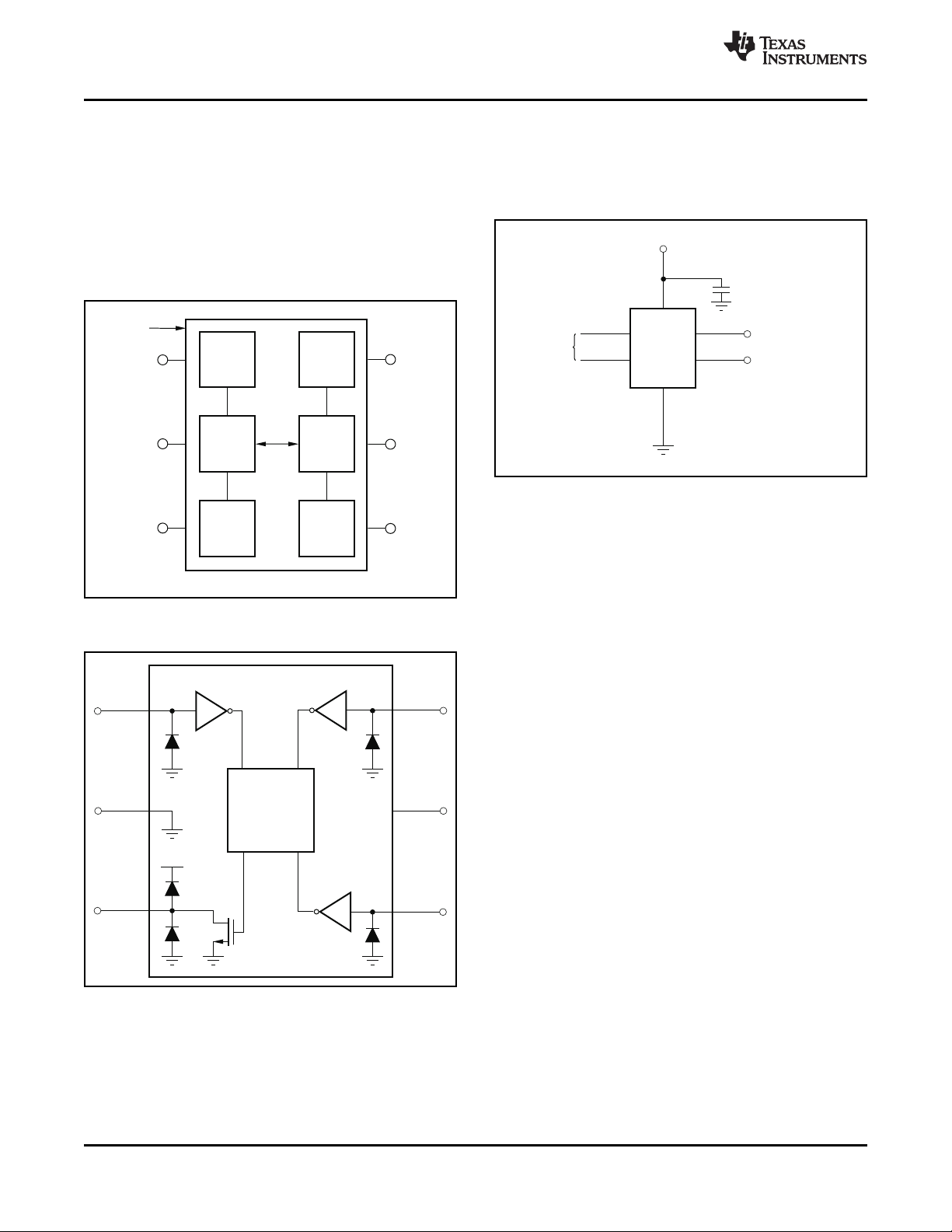
TMP1
12
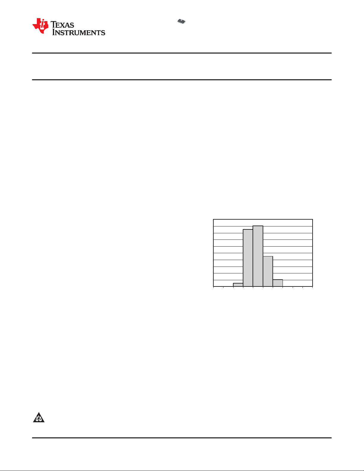
Population
-0.50
-
0.42
-0.34
-0.26
-0.18
-
0.10
-0.02
0.06
0.14
0.22
0.30
TemperatureError( C)°
TMP112
www.ti.com
......................................................................................................................................................... SBOS473B – MARCH 2009 – REVISED JUNE 2009
High-Accuracy, Low-Power, Digital Temperature Sensor
With SMBus™/Two-Wire Serial Interface in SOT563
1
FEATURES DESCRIPTION
23
• TINY SOT563 PACKAGE
• ACCURACY:
0.5 ° C (max) from 0 ° C to +65 ° C
1.0 ° C (max) from – 40 ° C to +125 ° C
• LOW QUIESCENT CURRENT:
10 µ A Active (max), 1 µ A Shutdown (max)
• SUPPLY RANGE: 1.4V to 3.6V
• RESOLUTION: 12 Bits
• DIGITAL OUTPUT: Two-Wire Serial Interface
APPLICATIONS
• PORTABLE AND BATTERY-POWERED
APPLICATIONS
• POWER-SUPPLY TEMPERATURE
MONITORING
• COMPUTER PERIPHERAL THERMAL
PROTECTION
• NOTEBOOK COMPUTERS
• BATTERY MANAGEMENT
• OFFICE MACHINES
• THERMOSTAT CONTROLS
• ELECTROMECHANICAL DEVICE
TEMPERATURES
• GENERAL TEMPERATURE MEASUREMENTS:
Industrial Controls
Test Equipment
Medical Instrumentation
The TMP112 is a two-wire, serial output temperature
sensor available in a tiny SOT563 package. Requiring
no external components, the TMP112 is capable of
reading temperatures to a resolution of 0.0625 ° C.
The TMP112 slope-specification allows users to
calibrate for higher accuracy.
The TMP112 features both SMBus and two-wire
interface compatibility, and allows up to four devices
on one bus. It also features an SMBus alert function.
The TMP112 is ideal for extended temperature
measurement in communication, computer,
consumer, environmental, industrial, and
instrumentation applications. It is specified for
operation over a temperature range of – 40 ° C to
+125 ° C.
TEMPERATURE ERROR AT +25 ° C
1
Please be aware that an important notice concerning availability, standard warranty, and use in critical applications of Texas
Instruments semiconductor products and disclaimers thereto appears at the end of this data sheet.
2 SMBus is a trademark of Intel, Inc.
3 All other trademarks are the property of their respective owners.
PRODUCTION DATA information is current as of publication date.
Products conform to specifications per the terms of the Texas
Instruments standard warranty. Production processing does not
necessarily include testing of all parameters.
Copyright © 2009, Texas Instruments Incorporated
1
2
3
6
5
4
SDA
V+
ADD0
SCL
GND
ALERT
OBS
TMP112
SBOS473B – MARCH 2009 – REVISED JUNE 2009 .........................................................................................................................................................
This integrated circuit can be damaged by ESD. Texas Instruments recommends that all integrated circuits be handled with
appropriate precautions. Failure to observe proper handling and installation procedures can cause damage.
ESD damage can range from subtle performance degradation to complete device failure. Precision integrated circuits may be more
susceptible to damage because very small parametric changes could cause the device not to meet its published specifications.
PACKAGE INFORMATION
PRODUCT PACKAGE-LEAD PACKAGE DESIGNATOR PACKAGE MARKING
TMP112 SOT563 DRL OBS
(1) For the most current package and ordering information, see the Package Option Addendum at the end of this document, or see the TI
web site at www.ti.com .
ABSOLUTE MAXIMUM RATINGS
PARAMETER TMP112 UNIT
Supply Voltage 5 V
Input Voltage, Pins 1, 4, and 6 – 0.5 to +5 V
Input Voltage, Pin 3 – 0.5 to (VS) + 0.5 V
Operating Temperature – 55 to +150 ° C
Storage Temperature – 60 to +150 ° C
Junction Temperature +150 ° C
Human Body Model (HBM) 2000 V
ESD Rating Charged Device Model (CDM) 1000 V
Machine Model (MM) 200 V
(1) Stresses above these ratings may cause permanent damage. Exposure to absolute maximum conditions for extended periods may
degrade device reliability. These are stress ratings only, and functional operation of the device at these or any other conditions beyond
those specified is not supported.
(1)
(1)
www.ti.com
PIN CONFIGURATION
DRL PACKAGE
SOT563
(TOP VIEW)
2 Submit Documentation Feedback Copyright © 2009, Texas Instruments Incorporated
Product Folder Link(s): TMP112

TMP112
www.ti.com
......................................................................................................................................................... SBOS473B – MARCH 2009 – REVISED JUNE 2009
ELECTRICAL CHARACTERISTICS
At TA= +25 ° C and VS= +1.4V to +3.6V, unless otherwise noted.
TMP112
PARAMETER CONDITIONS MIN TYP MAX UNIT
TEMPERATURE INPUT
Range – 40 +125 ° C
Accuracy (Temperature Error) +25 ° C, VS= 3.3V – 0.5 – 0.1 +0.3 ° C
0 ° C to +65 ° C, VS= 3.3V – 0.5 +0.5 ° C
– 40 ° C to +125 ° C – 1.0 1.0 ° C
vs Supply – 40 ° C to +125 ° C +0.0625 ± 0.25 ° C/V
Long-Term Stability 3000 Hours < 1 LSB
Resolution (LSB) 0.0625 ° C
DIGITAL INPUT/OUTPUT
Input Logic Levels:
V
IH
V
IL
Input Current I
IN
0 < VIN< 3.6V 1 µ A
Output Logic Levels:
V
SDA V+ > 2V, IOL= 3mA 0 0.4 V
OL
V+ < 2V, IOL= 3mA 0 0.2 (V+) V
V
ALERT V+ > 2V, IOL= 3mA 0 0.4 V
OL
V+ < 2V, IOL= 3mA 0 0.2 (V+) V
Resolution 12 Bits
Conversion Time 26 35 ms
Conversion Modes CR1 = 0, CR0 = 0 0.25 Conv/s
CR1 = 0, CR0 = 1 1 Conv/s
CR1 = 1, CR0 = 0 (default) 4 Conv/s
CR1 = 1, CR0 = 1 8 Conv/s
Timeout Time 30 40 ms
POWER SUPPLY
Operating Supply Range +1.4 +3.6 V
Quiescent Current I
Serial Bus Inactive, CR1 = 1, CR0 = 0 (default) 7 10 µ A
Q
Serial Bus Active, SCL Frequency = 400kHz 15 µ A
Serial Bus Active, SCL Frequency = 3.4MHz 85 µ A
Shutdown Current I
SD
Serial Bus Inactive 0.5 1 µ A
Serial Bus Active, SCL Frequency = 400kHz 10 µ A
Serial Bus Active, SCL Frequency = 3.4MHz 80 µ A
TEMPERATURE RANGE
Specified Range – 40 +125 ° C
Operating Range – 55 +150 ° C
Thermal Resistance θ
JA
SOT563 JEDEC Low-K Board 260 ° C/W
0.7 (V+) 3.6 V
– 0.5 0.3 (V+) V
Copyright © 2009, Texas Instruments Incorporated Submit Documentation Feedback 3
Product Folder Link(s): TMP112
Population
-0.50
-
0.42
-0.34
-0.26
-0.18
-
0.10
-0.02
0.06
0.14
0.22
0.30
TemperatureError( C)°
-0.250
-0.225
-
0.200
-0.175
-0.150
-
0.125
-0.100
-0.075
-
0.050
-0.025
0
0.025
0.050
0.075
0.100
0.125
0.150
0.175
0.200
0.225
0.250
AccuracyvsSupply( C/V)°
Population
1.0
0.8
0.6
0.4
0.2
0
0.2
0.4
0.6
0.8
1.0
-
-
-
-
-
T
emperatureError( C)
°
Temperature( C)°
-50 -25 0 25 50
75
100 125
20
18
16
14
12
10
8
6
4
2
0
Temperature( C)°
-60 -20 40 60 140 160
I (m
A)
Q
3.6VSupply
-40 0 20 80 100 120
1.4VSupply
10
9
8
7
6
5
4
3
2
1
0
Temperature( C)°
-60 -40 0 40 140 160
I (mA)
SD
3.6VSupply
1.4VSupply
-20 20 60 80 100 120
100
90
80
70
60
50
40
30
20
10
0
BusFrequency(Hz)
1k 10k 100k 1M 10M
I ( A)m
Q
- °55 C
+25 C°
+125 C°
TMP112
SBOS473B – MARCH 2009 – REVISED JUNE 2009 .........................................................................................................................................................
www.ti.com
TYPICAL CHARACTERISTICS
At TA= +25 ° C and V+ = 3.3V, unless otherwise noted.
TEMPERATURE ERROR AT +25 ° C ACCURACY vs SUPPLY
Figure 1. Figure 2.
TEMPERATURE ERROR vs TEMPERATURE (Four Conversions per Second)
QUIESCENT CURRENT vs TEMPERATURE
Figure 3. Figure 4.
SHUTDOWN CURRENT vs TEMPERATURE (Temperature at 3.3V Supply)
4 Submit Documentation Feedback Copyright © 2009, Texas Instruments Incorporated
Figure 5. Figure 6.
QUIESCENT CURRENT vs BUS FREQUENCY
Product Folder Link(s): TMP112
40
38
36
34
32
30
28
26
24
22
20
Temperature( C)°
-60 -20 40 60 140 160
ConversionTime(ms)
3.6VSupply
1.4VSupply
-40 200 80 100 120
TMP112
www.ti.com
......................................................................................................................................................... SBOS473B – MARCH 2009 – REVISED JUNE 2009
TYPICAL CHARACTERISTICS (continued)
At TA= +25 ° C and V+ = 3.3V, unless otherwise noted.
CONVERSION TIME vs TEMPERATURE
Figure 7.
Copyright © 2009, Texas Instruments Incorporated Submit Documentation Feedback 5
Product Folder Link(s): TMP112
TMP112
0.01mF
V+
GND
2
5
3
ALERT
(Output)
4
ADD0
1
SCL
6
SDA
To
Two-Wire
Controller
NOTE:SCL,SDA,andALERT
pinsrequirepull-upresistors.
Diode
Temp.
Sensor
DS
A/D
Converter
OSC
Control
Logic
Serial
Interface
Config.
andTemp.
Register
TMP112
Temperature
SCL
1
3
6
4
ALERT
SDA
GND
2 5
V+
ADD0
ALERT
Core
SCL
GND
V+
A0
V+
SDA
TMP112
TMP112
SBOS473B – MARCH 2009 – REVISED JUNE 2009 .........................................................................................................................................................
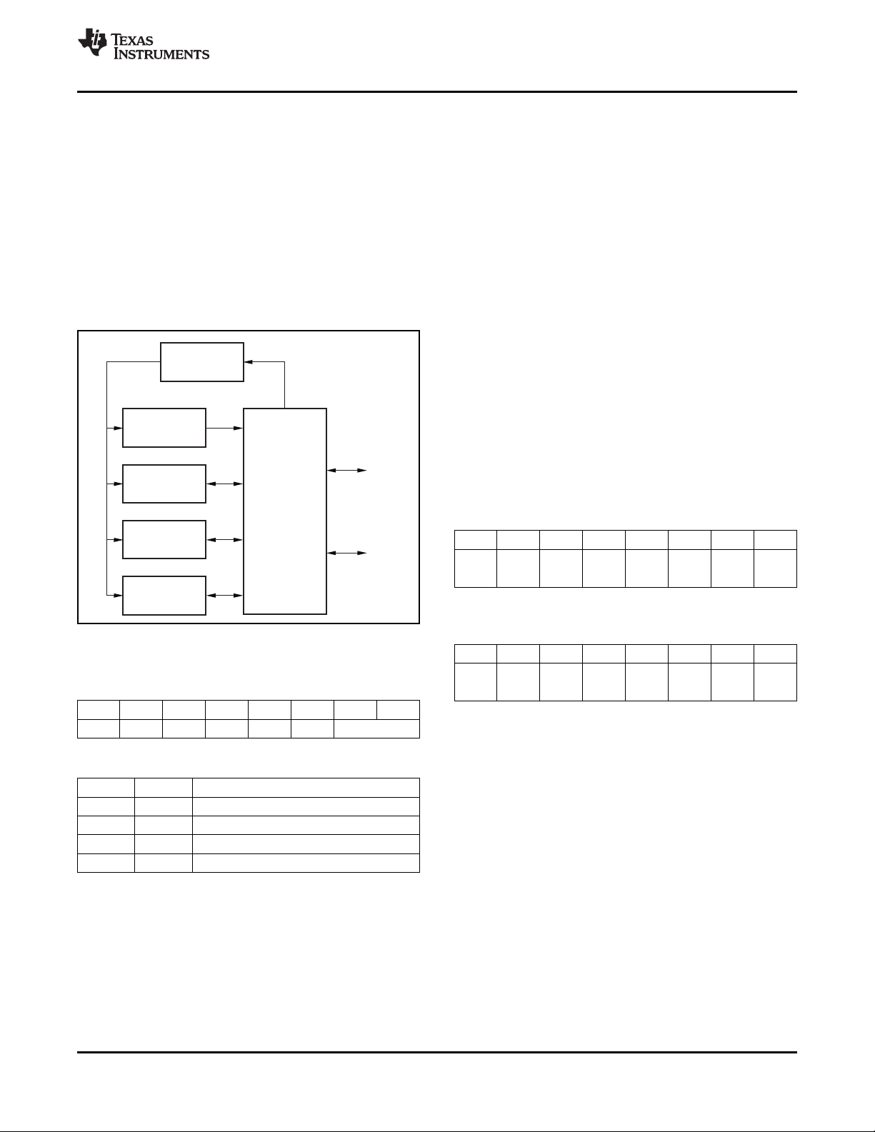
APPLICATION INFORMATION
The TMP112 is a digital temperature sensor that is
optimal for thermal-management and
thermal-protection applications. A block diagram of
the TMP112 is shown in Figure 8 . The TMP112 is
two-wire- and SMBus interface-compatible, and is
specified over an operating temperature range of
– 40 ° C to +125 ° C. Figure 9 illustrates the ESD
protection circuitry contained in the TMP112.
Figure 8. Internal Block Diagram
www.ti.com
Pull-up resistors are required on SCL, SDA, and
ALERT. A 0.01 µ F bypass capacitor is recommended,
as shown in Figure 10 .
Figure 10. Typical Connections
The temperature sensor in the TMP112 is the chip
itself. Thermal paths run through the package leads
as well as the plastic package. The lower thermal
resistance of metal causes the leads to provide the
primary thermal path.
To maintain accuracy in applications that require air
or surface temperature measurement, care should be
taken to isolate the package and leads from ambient
air temperature. A thermally-conductive adhesive is
helpful in achieving accurate surface temperature
measurement.
6 Submit Documentation Feedback Copyright © 2009, Texas Instruments Incorporated
Figure 9. Equivalent Internal ESD Circuitry
Product Folder Link(s): TMP112
I/O
Control
Interface
SCL
SDA
Temperature
Register
Configuration
Register
T
LOW
Register
T
HIGH
Register
Pointer
Register
TMP112
www.ti.com
......................................................................................................................................................... SBOS473B – MARCH 2009 – REVISED JUNE 2009
POINTER REGISTER TEMPERATURE REGISTER
Figure 11 shows the internal register structure of the The Temperature Register of the TMP112 is
TMP112. The 8-bit Pointer Register of the device is configured as a 12-bit, read-only register
used to address a given data register. The Pointer (Configuration Register EM bit = '0'; see the Extended
Register uses the two LSBs (see Table 11 ) to identify Mode section), or as a 13-bit, read-only register
which of the data registers should respond to a read (Configuration Register EM bit = '1') that stores the
or write command. Table 1 identifies the bits of the output of the most recent conversion. Two bytes must
Pointer Register byte. During a write command, P2 be read to obtain data, and are described in Table 3
through P7 must always be '0'. Table 2 describes the and Table 4 . Note that byte 1 is the most significant
pointer address of the registers available in the byte (MSB), followed by byte 2, the least significant
TMP112. The power-up reset value of P1/P0 is '00'. byte (LSB). The first 12 bits (13 bits in Extended
By default, the TMP112 reads the temperature on mode) are used to indicate temperature. The least
power-up. significant byte does not have to be read if that
information is not needed. The data format for temperature is summarized in Table 5 and Table 6 . One LSB equals 0.0625 ° C. Negative numbers are represented in binary twos complement format. Following power-up or reset, the Temperature Register reads 0 ° C until the first conversion is complete. Bit D0 of byte 2 indicates Normal mode (EM bit = '0') or Extended mode (EM bit = '1'), and can be used to distinguish between the two temperature register data formats. The unused bits in the Temperature Register always read '0'.
Figure 11. Internal Register Structure
Table 1. Pointer Register Byte
P7 P6 P5 P4 P3 P2 P1 P0
0 0 0 0 0 0 Register Bits
Table 2. Pointer Addresses
P1 P0 REGISTER
0 0 Temperature Register (Read Only)
0 1 Configuration Register (Read/Write)
1 0 T
1 1 T
Register (Read/Write)
LOW
Register (Read/Write)
HIGH
Table 3. Byte 1 of Temperature Register
D7 D6 D5 D4 D3 D2 D1 D0
T11 T10 T9 T8 T7 T6 T5 T4
(T12) (T11) (T10) (T9) (T8) (T7) (T6) (T5)
(1) Extended mode 13-bit configuration shown in parentheses.
Table 4. Byte 2 of Temperature Register
D7 D6 D5 D4 D3 D2 D1 D0
T3 T2 T1 T0 0 0 0 0
(T4) (T3) (T2) (T1) (T0) (0) (0) (1)
(1) Extended mode 13-bit configuration shown in parentheses.
(1)
(1)
Copyright © 2009, Texas Instruments Incorporated Submit Documentation Feedback 7
Product Folder Link(s): TMP112
TMP112
SBOS473B – MARCH 2009 – REVISED JUNE 2009 .........................................................................................................................................................
Table 5. 12-Bit Temperature Data Format
TEMPERATURE ( ° C) DIGITAL OUTPUT (BINARY) HEX
128 0111 1111 1111 7FF
127.9375 0111 1111 1111 7FF
100 0110 0100 0000 640
80 0101 0000 0000 500
75 0100 1011 0000 4B0
50 0011 0010 0000 320
25 0001 1001 0000 190
0.25 0000 0000 0100 004
0 0000 0000 0000 000
– 0.25 1111 1111 1100 FFC
– 25 1110 0111 0000 E70
– 55 1100 1001 0000 C90
(1) The resolution for the Temp ADC in Internal Temperature mode is 0.0625 ° C/count.
(1)
For positive temperatures (for example, +50 ° C):
Twos complement is not performed on positive numbers. Therefore, simply convert the number to binary
code with the 12-bit, left-justified format, and MSB = 0 to denote a positive sign.
Example: (+50 ° C)/(0.0625 ° C/count) = 800 = 320h = 0011 0010 0000
For negative temperatures (for example, – 25 ° C):
Generate the twos complement of a negative number by complementing the absolute value binary number
and adding 1. Denote a negative number with MSB = 1.
Example: (| – 25 ° C|)/(0.0625 ° C/count) = 400 = 190h = 0001 1001 0000
Twos complement format: 1110 0110 1111 + 1 = 1110 0111 0000
www.ti.com
Table 6. 13-Bit Temperature Data Format
TEMPERATURE ( ° C) DIGITAL OUTPUT (BINARY) HEX
150 0 1001 0110 0000 0960
128 0 1000 0000 0000 0800
127.9375 0 0111 1111 1111 07FF
100 0 0110 0100 0000 0640
80 0 0101 0000 0000 0500
75 0 0100 1011 0000 04B0
50 0 0011 0010 0000 0320
25 0 0001 1001 0000 0190
0.25 0 0000 0000 0100 0004
0 0 0000 0000 0000 0000
– 0.25 1 1111 1111 1100 1FFC
– 25 1 1110 0111 0000 1E70
– 55 1 1100 1001 0000 1C90
8 Submit Documentation Feedback Copyright © 2009, Texas Instruments Incorporated
Product Folder Link(s): TMP112

Startup Startof
Conversion
Delay
(1)
26ms
26ms
TMP112
www.ti.com
......................................................................................................................................................... SBOS473B – MARCH 2009 – REVISED JUNE 2009
CONFIGURATION REGISTER CONVERSION RATE
The Configuration Register is a 16-bit read/write The conversion rate bits, CR1 and CR0, configure the
register used to store bits that control the operational TMP112 for conversion rates of 8Hz, 4Hz, 1Hz, or
modes of the temperature sensor. Read/write 0.25Hz. The default rate is 4Hz. The TMP112 has a
operations are performed MSB first. The format and typical conversion time of 26ms. To achieve different
power-up/reset values of the Configuration Register conversion rates, the TMP112 makes a conversion
are shown in Table 7 . For compatibility, the first byte and then powers down and waits for the appropriate
corresponds to the Configuration Register in the delay set by CR1 and CR0. Table 8 shows the
TMP75 and TMP275 . All registers are updated byte settings for CR1 and CR0.
by byte.
Table 8. Conversion Rate Settings
Table 7. Configuration and Power-Up/Reset
Formats
BYTE D7 D6 D5 D4 D3 D2 D1 D0
OS R1 R0 F1 F0 POL TM SD
1
2
0 1 1 0 0 0 0 0
CR1 CR0 AL EM 0 0 0 0
1 0 1 0 0 0 0 0
EXTENDED MODE (EM)
The Extended mode bit configures the device for conversion is 40 µ A (typical at +27 ° C). The quiescent
Normal mode operation (EM = 0) or Extended mode current during delay is 2.2 µ A (typical at +27 ° C).
operation (EM = 1). In Normal mode, the
Temperature Register and high- and low-limit
registers use a 12-bit data format. Normal mode is
used to make the TMP112 compatible with the
TMP75 .
Extended mode (EM = 1) allows measurement of
temperatures above +128 ° C by configuring the
Temperature Register, and high- and low-limit
registers, for 13-bit data format.
CR1 CR0 CONVERSION RATE
0 0 0.25Hz
0 1 1Hz
1 0 4Hz (default)
1 1 8Hz
After a power-up or general-call reset, the TMP112
immediately starts a conversion, as shown in
Figure 12 . The first result is available after 26ms
(typical). The active quiescent current during
ALERT (AL Bit)
The AL bit is a read-only function. Reading the AL bit
(1) Delay is set by CR1 and CR0.
Figure 12. Conversion Start
provides information about the comparator mode
status. The state of the POL bit inverts the polarity of
data returned from the AL bit. For POL = 0, the AL bit
reads as '1' until the temperature equals or exceeds
T
for the programmed number of consecutive
HIGH
faults, causing the AL bit to read as '0'. The AL bit
continues to read as '0' until the temperature falls
below T
for the programmed number of
LOW
consecutive faults, when it again reads as '1'. The
status of the TM bit does not affect the status of the
AL bit.
SHUTDOWN MODE (SD)
The Shutdown mode bit saves maximum power by
shutting down all device circuitry other than the serial
interface, reducing current consumption to typically
less than 0.5 µ A. Shutdown mode is enabled when
the SD bit = '1'; the device shuts down when current
conversion is completed. When SD = '0', the device
maintains a continuous conversion state.
THERMOSTAT MODE (TM)
The Thermostat mode bit indicates to the device
whether to operate in Comparator mode (TM = 0) or
Interrupt mode (TM = 1). For more information on
Comparator and Interrupt modes, see the High- and
Low-Limit Registers section.
Copyright © 2009, Texas Instruments Incorporated Submit Documentation Feedback 9
Product Folder Link(s): TMP112

Measured
Temperature
T
HIGH
T
LOW
TMP112 ALERTPIN
(ComparatorMode)
POL=0
TMP112 ALERTPIN
(InterruptMode)
POL=0
TMP112 ALERTPIN
(ComparatorMode)
POL=1
TMP112 ALERTPIN
(InterruptMode)
POL=1
Read Read
Time
Read
TMP112
SBOS473B – MARCH 2009 – REVISED JUNE 2009 .........................................................................................................................................................
www.ti.com
POLARITY (POL) CONVERTER RESOLUTION (R1/R0)
The Polarity bit allows the user to adjust the polarity R1/R0 are read-only bits. The TMP112 converter
of the ALERT pin output. If POL = 0, the ALERT pin resolution is set on start up to '11'. This sets the
becomes active low, as shown in Figure 13 . For POL temperature register to a 12 bit-resolution.
= 1, the ALERT pin becomes active high, and the
state of the ALERT pin is inverted.
ONE-SHOT/CONVERSION READY (OS)
The TMP112 features a One-Shot Temperature
Measurement mode. When the device is in Shutdown
mode, writing a '1' to the OS bit starts a single
temperature conversion. During the conversion, the
OS bit reads '0'. The device returns to the shutdown
state at the completion of the single conversion. After
the conversion, the OS bit reads '1'. This feature is
useful for reducing power consumption in the
TMP112 when continuous temperature monitoring is
not required.
As a result of the short conversion time, the TMP112
can achieve a higher conversion rate. A single
conversion typically takes 26ms and a read can take
place in less than 20 µ s. When using One-Shot mode,
30 or more conversions per second are possible.
HIGH- AND LOW-LIMIT REGISTERS
In Comparator mode (TM = 0), the ALERT pin
becomes active when the temperature equals or
exceeds the value in T
consecutive number of faults according to fault bits
F1 and F0. The ALERT pin remains active until the
Figure 13. Output Transfer Function Diagrams
temperature falls below the indicated T
the same number of faults.
In Interrupt mode (TM = 1), the ALERT pin becomes
FAULT QUEUE (F1/F0)
A fault condition exists when the measured
temperature exceeds the user-defined limits set in the
T
and T
HIGH
fault conditions required to generate an alert may be
programmed using the fault queue. The fault queue is
provided to prevent a false alert as a result of
environmental noise. The fault queue requires
consecutive fault measurements in order to trigger
the alert function. Table 9 defines the number of
measured faults that may be programmed to trigger
an alert condition in the device. For T
register format and byte order, see the High- and
Low-Limit Registers section.
F1 F0 CONSECUTIVE FAULTS
0 0 1
0 1 2
1 0 4
1 1 6
10 Submit Documentation Feedback Copyright © 2009, Texas Instruments Incorporated
registers. Additionally, the number of
LOW
Table 9. TMP112 Fault Settings
and T
HIGH
Product Folder Link(s): TMP112
LOW
active when the temperature equals or exceeds the
value in T
for a consecutive number of fault
HIGH
conditions (as shown in Table 9 ). The ALERT pin
remains active until a read operation of any register
occurs, or the device successfully responds to the
SMBus Alert Response address. The ALERT pin is
also cleared if the device is placed in Shutdown
mode. Once the ALERT pin is cleared, it becomes
active again only when temperature falls below T
and remains active until cleared by a read operation
of any register or a successful response to the
SMBus Alert Response address. Once the ALERT
pin is cleared, the above cycle repeats, with the
ALERT pin becoming active when the temperature
equals or exceeds T
. The ALERT pin can also be
HIGH
cleared by resetting the device with the General Call
Reset command. This action also clears the state of
the internal registers in the device, returning the
device to Comparator mode (TM = 0).
and generates a
HIGH
value for
LOW
,
LOW

TMP112
www.ti.com
......................................................................................................................................................... SBOS473B – MARCH 2009 – REVISED JUNE 2009
Both operating modes are represented in Figure 13 .
Table 10 and Table 11 describe the format for the
T
and T
HIGH
registers. Note that the most
LOW
significant byte is sent first, followed by the least
significant byte. Power-up reset values for T
T
are:
LOW
• T
• T
The format of the data for T
= +80 ° C
HIGH
= +75 ° C
LOW
and T
HIGH
LOW
is the same
and
HIGH
as for the Temperature Register.
Table 10. Bytes 1 and 2 of T
BYTE D7 D6 D5 D4 D3 D2 D1 D0
H11 H10 H9 H8 H7 H6 H5 H4
1
(H12) (H11) (H10) (H9) (H8) (H7) (H6) (H5)
BYTE D7 D6 D5 D4 D3 D2 D1 D0
H3 H2 H1 H0 0 0 0 0
2
(H4) (H3) (H2) (H1) (H0) (0) (0) (0)
(1) Extended mode 13-bit configuration shown in parenthesis.
Table 11. Bytes 1 and 2 of T
BYTE D7 D6 D5 D4 D3 D2 D1 D0
L11 L10 L9 L8 L7 L6 L5 L4
1
(L12) (L11) (L10) (L9) (L8) (L7) (L6) (L5)
BYTE D7 D6 D5 D4 D3 D2 D1 D0
L3 L2 L1 L0 0 0 0 0
2
(L4) (L3) (L2) (L1) (L0) (0) (0) (0)
(1) Extended mode 13-bit configuration shown in parenthesis.
Register
HIGH
Register
LOW
(1)
(1)
SERIAL INTERFACE
The TMP112 operates as a slave device only on the
two-wire bus and SMBus. Connections to the bus are
made via the open-drain I/O lines SDA and SCL. The
SDA and SCL pins feature integrated spike
suppression filters and Schmitt triggers to minimize
the effects of input spikes and bus noise. The
TMP112 supports the transmission protocol for both
fast (1kHz to 400kHz) and high-speed (1kHz to
3.4MHz) modes. All data bytes are transmitted MSB
first.
SERIAL BUS ADDRESS
To communicate with the TMP112, the master must
first address slave devices via a slave address byte.
The slave address byte consists of seven address
bits, and a direction bit indicating the intent of
executing a read or write operation.
The TMP112 features an address pin to allow up to
four devices to be addressed on a single bus.
Table 12 describes the pin logic levels used to
properly connect up to four devices.
Table 12. Address Pin and Slave Addresses
DEVICE TWO-WIRE
ADDRESS A0 PIN CONNECTION
1001000 Ground
1001001 V+
1001010 SDA
1001011 SCL
BUS OVERVIEW
The device that initiates the transfer is called a
master, and the devices controlled by the master are
slaves. The bus must be controlled by a master
device that generates the serial clock (SCL), controls
the bus access, and generates the START and STOP
conditions.
To address a specific device, a START condition is
initiated, indicated by pulling the data-line (SDA) from
a high to low logic level while SCL is high. All slaves
on the bus shift in the slave address byte on the
rising edge of the clock, with the last bit indicating
whether a read or write operation is intended. During
the ninth clock pulse, the slave being addressed
responds to the master by generating an
Acknowledge and pulling SDA low.
Data transfer is then initiated and sent over eight
clock pulses followed by an Acknowledge Bit. During
data transfer SDA must remain stable while SCL is
high, because any change in SDA while SCL is high
is interpreted as a START or STOP signal.
Once all data have been transferred, the master
generates a STOP condition indicated by pulling SDA
from low to high, while SCL is high.
WRITING/READING OPERATION
Accessing a particular register on the TMP112 is
accomplished by writing the appropriate value to the
Pointer Register. The value for the Pointer Register is
the first byte transferred after the slave address byte
with the R/ W bit low. Every write operation to the
TMP112 requires a value for the Pointer Register
(see Figure 16 ).
When reading from the TMP112, the last value stored
in the Pointer Register by a write operation is used to
determine which register is read by a read operation.
To change the register pointer for a read operation, a
new value must be written to the Pointer Register.
This action is accomplished by issuing a slave
address byte with the R/ W bit low, followed by the
Pointer Register byte. No additional data are
required. The master can then generate a START
condition and send the slave address byte with the
R/ W bit high to initiate the read command. See
Figure 17 for details of this sequence. If repeated
Copyright © 2009, Texas Instruments Incorporated Submit Documentation Feedback 11
Product Folder Link(s): TMP112

TMP112
SBOS473B – MARCH 2009 – REVISED JUNE 2009 .........................................................................................................................................................
www.ti.com
reads from the same register are desired, it is not For POL = '0', this bit is low if the temperature is
necessary to continually send the Pointer Register greater than or equal to T
bytes, because the TMP112 remembers the Pointer temperature is less than T
; this bit is high if the
HIGH
. The polarity of this bit
LOW
Register value until it is changed by the next write is inverted if POL = '1'. Refer to Figure 18 for details
operation. of this sequence.
Note that register bytes are sent with the most If multiple devices on the bus respond to the SMBus
significant byte first, followed by the least significant Alert command, arbitration during the slave address
byte. portion of the SMBus Alert command determines
which device clears its ALERT status. The device
SLAVE MODE OPERATIONS
The TMP112 can operate as a slave receiver or slave
transmitter. As a slave device, the TMP112 never
drives the SCL line.
Slave Receiver Mode:
The first byte transmitted by the master is the slave
address, with the R/ W bit low. The TMP112 then
acknowledges reception of a valid address. The next
byte transmitted by the master is the Pointer
Register. The TMP112 then acknowledges reception
of the Pointer Register byte. The next byte or bytes
are written to the register addressed by the Pointer
Register. The TMP112 acknowledges reception of
each data byte. The master can terminate data
transfer by generating a START or STOP condition.
Slave Transmitter Mode:
The first byte transmitted by the master is the slave
address, with the R/ W bit high. The slave
acknowledges reception of a valid slave address. The
next byte is transmitted by the slave and is the most
significant byte of the register indicated by the Pointer
Register. The master acknowledges reception of the
data byte. The next byte transmitted by the slave is
the least significant byte. The master acknowledges
reception of the data byte. The master can terminate
data transfer by generating a Not-Acknowledge on
reception of any data byte, or generating a START or
STOP condition.
SMBus ALERT FUNCTION
The TMP112 supports the SMBus Alert function.
When the TMP112 operates in Interrupt mode (TM =
'1'), the ALERT pin may be connected as an SMBus
Alert signal. When a master senses that an ALERT
condition is present on the ALERT line, the master
sends an SMBus Alert command (00011001) to the
bus. If the ALERT pin is active, the device
acknowledges the SMBus Alert command and
with the lowest two-wire address wins the arbitration.
If the TMP112 wins the arbitration, its ALERT pin
becomes inactive at the completion of the SMBus
Alert command. If the TMP112 loses the arbitration,
its ALERT pin remains active.
GENERAL CALL
The TMP112 responds to a two-wire General Call
address (0000000) if the eighth bit is '0'. The device
acknowledges the General Call address and
responds to commands in the second byte. If the
second byte is 00000110, the TMP112 internal
registers are reset to power-up values. The TMP112
does not support the General Address acquire
command.
HIGH-SPEED (Hs) MODE
In order for the two-wire bus to operate at frequencies
above 400kHz, the master device must issue an
Hs-mode master code (00001xxx) as the first byte
after a START condition to switch the bus to
high-speed operation. The TMP112 does not
acknowledge this byte, but switches its input filters on
SDA and SCL and its output filters on SDA to operate
in Hs-mode, allowing transfers at up to 3.4MHz. After
the Hs-mode master code has been issued, the
master transmits a two-wire slave address to initiate a
data transfer operation. The bus continues to operate
in Hs-mode until a STOP condition occurs on the bus.
Upon receiving the STOP condition, the TMP112
switches the input and output filters back to
fast-mode operation.
TIMEOUT FUNCTION
The TMP112 resets the serial interface if SCL is held
low for 30ms (typ). The TMP112 releases the bus if it
is pulled low and waits for a START condition. To
avoid activating the timeout function, it is necessary
to maintain a communication speed of at least 1kHz
for SCL operating frequency.
responds by returning its slave address on the SDA
line. The eighth bit (LSB) of the slave address byte
indicates if the ALERT condition was caused by the
temperature exceeding T
or falling below T
HIGH
.
LOW
12 Submit Documentation Feedback Copyright © 2009, Texas Instruments Incorporated
Product Folder Link(s): TMP112

TMP112
SCL SDA
GND V+
ALERT ADD0
C
F
10nF³
R
F
5k£ W
SupplyVoltage
TMP112
www.ti.com
NOISE
The TMP112 is a very low-power device and
generates very low noise on the supply bus. Applying
an RC filter to the V+ pin of the TMP112 can further
......................................................................................................................................................... SBOS473B – MARCH 2009 – REVISED JUNE 2009
Start Data Transfer: A change in the state of the
SDA line, from high to low, while the SCL line is high,
defines a START condition. Each data transfer is
initiated with a START condition.
reduce any noise that the TMP112 might propagate Stop Data Transfer: A change in the state of the
to other components. R
than 5k Ω and C
should be greater than 10nF. defines a STOP condition. Each data transfer is
F
in Figure 14 should be less SDA line from low to high while the SCL line is high
F
terminated with a repeated START or STOP
condition.
Data Transfer: The number of data bytes transferred
between a START and a STOP condition is not
limited and is determined by the master device. It is
also possible to use the TMP112 for single byte
updates. To update only the MS byte, terminate the
communication by issuing a START or STOP
communication on the bus.
Acknowledge: Each receiving device, when
addressed, is obliged to generate an Acknowledge
bit. A device that acknowledges must pull down the
SDA line during the Acknowledge clock pulse in such
a way that the SDA line is stable low during the high
Figure 14. Noise Reduction Techniques
period of the Acknowledge clock pulse. Setup and
hold times must be taken into account. On a master
TIMING DIAGRAMS
The TMP112 is two-wire and SMBus compatible.
Figure 15 to Figure 18 describe the various
receive, the termination of the data transfer can be
signaled by the master generating a
Not-Acknowledge ('1') on the last byte that has been
transmitted by the slave.
operations on the TMP112. Parameters for Figure 15
are defined in Table 13 . Bus definitions are:
Bus Idle: Both SDA and SCL lines remain high.
Table 13. Timing Diagram Definitions
FAST MODE HIGH-SPEED MODE
PARAMETER TEST CONDITIONS MIN MAX MIN MAX UNIT
f
(SCL)
f
(SCL)
t
(BUF)
t
(HDSTA)
t
(SUSTA)
t
(SUSTO)
t
(HDDAT)
t
(SUDAT)
t
(LOW)
t
(LOW)
t
(HIGH)
t
F
t
R
t
R
SCL Operating Frequency, VS> 1.7V 0.001 0.4 0.001 3.4 MHz
SCL Operating Frequency, VS< 1.7V 0.001 0.4 0.001 2.75 MHz
Bus Free Time Between STOP and START
Hold time after repeated START condition.
After this period, the first clock is generated.
Repeated START Condition Setup Time 100 100 ns
STOP Condition Setup Time 100 100 ns
SCL Clock Low Period, VS> 1.7V 1300 160 ns
SCL Clock Low Period, VS< 1.7V 1300 200 ns
Clock/Data Rise Time for SCLK ≤ 100kHz 1000 ns
Condition
Data Hold Time 0 0 ns
Data Setup Time 100 10 ns
SCL Clock High Period 600 60 ns
Clock/Data Fall Time 300 ns
Clock/Data Rise Time 300 160 ns
600 160 ns
100 100 ns
Copyright © 2009, Texas Instruments Incorporated Submit Documentation Feedback 13
Product Folder Link(s): TMP112

SCL
SDA
t
(LOW)
t
R
t
F
t
(HDSTA)
t
(HDSTA)
t
(HDDAT)
t
(BUF)
t
(SUDAT)
t
(HIGH)
t
(SUSTA)
t
(SUSTO)
P S S P
Frame1Two-WireSlaveAddressByte
Frame2PointerRegisterByte
Frame4DataByte2
1
StartBy
Master
ACKBy
TMP112
ACKBy
TMP112
ACKBy
TMP112
StopBy
Master
1 9 1
1
D7 D6 D5 D4 D3 D2 D1 D0
9
Frame3DataByte1
ACKBy
TMP112
1
D7
SDA
(Continued)
SCL
(Continued)
D6 D5 D4 D3 D2 D1 D0
9
9
SDA
SCL
0 0 1 0
A1
(1)A0(1)
R/W 0 0 0 0 0 0 P1 P0 ¼
¼
NOTE:(1)ThevaluesofA0andA1aredeterminedbytheADD0pin.
TMP112
SBOS473B – MARCH 2009 – REVISED JUNE 2009 .........................................................................................................................................................
TWO-WIRE TIMING DIAGRAMS
www.ti.com
Figure 15. Two-Wire Timing Diagram
Figure 16. Two-Wire Timing Diagram for Write Word Format
14 Submit Documentation Feedback Copyright © 2009, Texas Instruments Incorporated
Product Folder Link(s): TMP112

Frame1Two-WireSlaveAddressByte Frame2PointerRegisterByte
1
StartBy
Master
ACKBy
TMP112
ACKBy
TMP112
Frame3Two-WireSlaveAddressByte Frame4DataByte1ReadRegister
StartBy
Master
ACKBy
TMP112
ACKBy
Master
(2)
From
TMP112
1 9 1
9
1 9 1
9
SDA
SCL
0 0 1 R/W
0 0 0 0 0 0 P1 P0
¼
¼
¼
SDA
(Continued)
SCL
(Continued)
SDA
(Continued)
SCL
(Continued)
1 0 0 1
0
A1
(1)A0(1)
0
A1
(1)A0(1)
R/W D7 D6 D5 D4 D3 D2 D1 D0
Frame5DataByte2ReadRegister
StopBy
Master
ACKBy
Master
(3)
From
TMP112
1
9
D7 D6 D5 D4 D3 D2 D1 D0
StopBy
Master
NOTE: (1)ThevaluesofA0andA1aredeterminedbytheADD0pin.
(2)MastershouldleaveSDAhightoterminateasingle-bytereadoperation.
(3)MastershouldleaveSDAhightoterminateatwo-bytereadoperation.
NOTE:(1)ThevaluesofA0andA1aredeterminedbytheADD0pin.
Frame1SMBusALERTResponseAddressByte Frame2SlaveAddressFromTMP112
StartBy
Master
ACKBy
TMP112
From
TMP112
NACKBy
Master
StopBy
Master
1 9 1
9
SDA
SCL
ALERT
0 0 0 1 1 0 0 R/
W 1 0 0 1 A1 A0
Status
TMP112
www.ti.com
......................................................................................................................................................... SBOS473B – MARCH 2009 – REVISED JUNE 2009
Figure 17. Two-Wire Timing Diagram for Read Word Format
Figure 18. Timing Diagram for SMBus ALERT
Copyright © 2009, Texas Instruments Incorporated Submit Documentation Feedback 15
Product Folder Link(s): TMP112

0.8
0.6
0.4
0.2
0
0.2
0.4
0.6
-
-
-
TemperatureError(
C)
°
Temperature( C)°
-40 -20 0 20 40 60 130
Slope1
MAX
Slope1
MIN
Slope2
MAX
Slope2
MIN
Slope3
MIN
100 11012080 9070503010-30 -10
Slope3
MAX
Accuracy =Acc + T SlopeD ´
(worst-case) 25°C)
uracy
(
TMP112
SBOS473B – MARCH 2009 – REVISED JUNE 2009 .........................................................................................................................................................
www.ti.com
CALIBRATING FOR IMPROVED ACCURACY
There are many temperature monitoring applications that require better than 0.5 ° C accuracy over a limited
temperature range. Knowing the offset of a temperature sensor at a given temperature in conjunction with the
average temperature span (slope) error over a fixed range makes it possible to achieve this improved accuracy.
The TMP112 has three distinct slope regions that conservatively approximate its inherent curvature:
1. Slope1 applies over – 40 ° C to +25 ° C
2. Slope2 applies over +25 ° C to +85 ° C
3. Slope3 applies over +85 ° C to +125 ° C
These slopes are defined in Table 14 and shown in Figure 19 .It is important to note that each slope is increasing
with respect to 25 ° C.
Table 14. Specifications for User-Calibrated Systems
PARAMETER CONDITION MIN MAX UNIT
Average Slope
(Temperature Error vs VS= +3.3, +25 ° C to +85 ° C 0 +5 m ° C/ ° C
Temperature)
(1)
(1) User-calibrated temperature accuracy can be within ± 1LSB because of quantization noise.
VS= +3.3, – 40 ° C to +25 ° C – 7 0 m ° C/ ° C
VS= +3.3, +85 ° C to +125 ° C 0 +8 m ° C/ ° C
Figure 19. Accuracy and Slope Curves versus Temperature
Equation 1 determines the worst-case accuracy at a specific temperature:
16 Submit Documentation Feedback Copyright © 2009, Texas Instruments Incorporated
(1)
Product Folder Link(s): TMP112

Accuracy =Accuracy + T Slope1D ´
MAX ( 15°Cto 25°C) (- 25°C) MAX
Accuracy =0.3 C+( 15 C 25 C)° -
MAX ( 15°Cto 25°C)-
° - °
-7
=+0.58°C
m°C
°C
Accuracy =Accuracy + T Slope2D ´
MAX (25°Cto 50°C) (25°C) MAX
Accuracy =0.3 C+(50 C 25 C)° ´
MAX (25°Cto 50°C)
° - °
5
=+0.425°C
m°C
°C
Accuracy =Accuracy + T Slope1D ´
MIN( 15°Cto 25°C) (- 25°C) MIN
Accuracy = 0.5 C+( 15 C 25 C)- ° -
MIN( 15°Cto 25°C)-
° - °
0
= 0.5- °C
m°C
°C
Accuracy =Accuracy + T Slope2D ´
MIN(25°Cto 50°C) (25°C) MIN
Accuracy = 0.5 C+(50 C 25 C)- °
MIN(25°Cto 50°C)
° - °
0
= 0.5- °C
m°C
°C
Accuracy =Accuracy + T Slope2D ´
MAX (25°Cto 100°C) ( MAX
+ T Slope3D ´
25°C) MAX
Accuracy =0.3 C+(85 C 25 C)°
MAX (25°Cto 100°C)
° - °
4.5
m°C
°C
+(100 C 85 C)° - °
8
=+0.690°C
m°C
°C
Accuracy =Accuracy + T Slope2D ´
MIN(25°Cto 100°C) ( MIN
+ T Slope3D ´
25°C) MIN
Accuracy = 0.5 C+(85 C 25 C)- ° -
MIN(25°Cto 100°C)
° °
0
m°C
°C
+(100 C 85 C)° - °
0
= 0.5- °C
m°C
°C
TMP112
www.ti.com
......................................................................................................................................................... SBOS473B – MARCH 2009 – REVISED JUNE 2009
EXAMPLE 1: Finding Worst-Case Accuracy From – 15 ° C to +50 ° C
As an example, if the user is concerned only about the temperature accuracy between – 15 ° C to +50 ° C, the
worst-case accuracy could be determined by using the two slope calculations of Equation 2 and Equation 4 :
The same calculations must be applied to the minimum case:
Based on the above calculations, a user can expect a worst-case accuracy of +0.58 ° C to – 0.5 ° C in the
temperature range of – 15 ° C to +50 ° C.
(2)
(3)
(4)
(5)
(6)
(7)
(8)
(9)
EXAMPLE 2: Finding Worst-Case Accuracy From +25 ° C to +100 ° C
If the desired temperature range falls in the region of slope 3, it is necessary to first calculate the worst-case
value from +25 ° C to +85 ° C and add it to the change in temperature multiplied by the span error of slope 3. As an
example, consider the temperature range of +25 ° C to +125 ° C as shown in Equation 10 :
Performing the same calculation for the minimum case is shown in Equation 12 :
(10)
(11)
(12)
(13)
Copyright © 2009, Texas Instruments Incorporated Submit Documentation Feedback 17
Product Folder Link(s): TMP112

Accuracy = (V 3.3V)± - ´
PSR S
+0.250°C
V
Accuracy = (1.8V 3.3V)± - ´
PSR
+0.250°C
V
=+0.375°C
0.8
0.6
0.4
0.2
0
0.2
0.4
0.6
-
-
-
TemperatureError( C)
°
Temperature( C)°
Slope1
MAX
Slope2
MAX
Slope3
MAX
Calibrationat+25 CRemovesOffset°
-40 -20 0 40 60 130100 11012080 90705020 3010-30 -10
TMP112
SBOS473B – MARCH 2009 – REVISED JUNE 2009 .........................................................................................................................................................
USING THE SLOPE SPECIFICATIONS WITH A
Using the previous example temperature range of
www.ti.com
1-POINT CALIBRATION 0 ° C to +50 ° C, the worst-case temperature error is
The initial accuracy assurance at +25 ° C with the
slope regions provides an accuracy that is high
enough for most applications; however, if higher
accuracy is desired, this increase can be achieved
with a 1-point calibration at +25 ° C. This calibration
removes the offset at room temperature, thereby
reducing the source of error in a TMP112
temperature reading down to the curvature. Figure 20 The superior accuracy that can be achieved with the
shows the error of a calibrated TMP112. TMP112 is complemented by its immunity to dc
now reduced to the worst-case slopes because the
offset at +25 ° C (that is, the maximum and minimum
temperature errors of +0.3 ° C and – 0.5 ° C) is removed.
Therefore, a user can expect the worst-case accuracy
to improve to +0.175 ° C.
Power-Supply Level Contribution to Accuracy
variations from a 3.3V supply voltage. This immunity
is important because it spares the user from having to
use another LDO to produce 3.3V to achieve
accuracy. Nevertheless, the noise quantization that
results from changing supply can add some slight
change in temperature measurement accuracy. As an
example, if the user chooses to operate at 1.8V, the
worst-case expected change in accuracy can be
calculated by Equation 14 :
(14)
(15)
Figure 20. Calibrated Accuracy and Slope Curves
versus Temperature
This example is a worst-case accuracy contribution
as a result of variation in power supply that should be
added to the accuracy + slope maximum.
18 Submit Documentation Feedback Copyright © 2009, Texas Instruments Incorporated
Product Folder Link(s): TMP112

TMP112
www.ti.com
......................................................................................................................................................... SBOS473B – MARCH 2009 – REVISED JUNE 2009
Revision History
NOTE: Page numbers for previous revisions may differ from page numbers in the current version.
Changes from Revision A (March 2009) to Revision B .................................................................................................. Page
• Changed footnote 1 of Table 14 .......................................................................................................................................... 16
• Clarified Example 1; extended worst-case accuracy to be from – 15 ° C to +50 ° C ............................................................... 17
• Corrected Equation 15 ......................................................................................................................................................... 18
Copyright © 2009, Texas Instruments Incorporated Submit Documentation Feedback 19
Product Folder Link(s): TMP112

PACKAGE OPTION ADDENDUM
www.ti.com 26-Jun-2009
PACKAGING INFORMATION
Orderable Device Status
(1)
Package
Type
Package
Drawing
Pins Package
Qty
Eco Plan
TMP112AIDRLR ACTIVE SOT DRL 6 4000 Green (RoHS &
(2)
Lead/Ball Finish MSL Peak Temp
CU NIPDAU Level-1-260C-UNLIM
(3)
no Sb/Br)
TMP112AIDRLT ACTIVE SOT DRL 6 250 Green (RoHS &
CU NIPDAU Level-1-260C-UNLIM
no Sb/Br)
(1)
The marketing statusvalues are defined as follows:
ACTIVE: Product devicerecommended for new designs.
LIFEBUY: TI hasannounced that the device will be discontinued, and alifetime-buy period is in effect.
NRND: Not recommended for new designs. Device is in production to support existing customers, but TI does not recommend using this part in
a new design.
PREVIEW: Device hasbeen announced but is not in production. Samples mayor may not be available.
OBSOLETE: TI hasdiscontinued the production of the device.
(2)
Eco Plan - The planned eco-friendly classification: Pb-Free (RoHS), Pb-Free (RoHS Exempt), or Green (RoHS & no Sb/Br) - please check
http://www.ti.com/productcontent for thelatest availability information and additional product content details.
TBD: The Pb-Free/Greenconversion plan has not been defined.
Pb-Free (RoHS): TI's terms "Lead-Free" or "Pb-Free" mean semiconductor products that are compatible with the current RoHS requirements
for all 6 substances, including the requirement that lead not exceed 0.1% by weight in homogeneous materials. Where designed to be soldered
at high temperatures,TI Pb-Free products are suitable for use in specifiedlead-free processes.
Pb-Free (RoHS Exempt): This component has a RoHS exemption for either 1) lead-based flip-chip solder bumps used between the die and
package, or 2) lead-based die adhesive used between the die and leadframe. The component is otherwise considered Pb-Free (RoHS
compatible) as definedabove.
Green (RoHS & no Sb/Br): TI defines "Green" to mean Pb-Free (RoHS compatible), and free of Bromine (Br) and Antimony (Sb) based flame
retardants (Br orSb do not exceed 0.1% by weight in homogeneousmaterial)
(3)
MSL, Peak Temp. -- The Moisture Sensitivity Level rating according to the JEDEC industry standard classifications, and peak solder
temperature.
Important Information and Disclaimer:The information provided on this page represents TI's knowledge and belief as of the date that it is
provided. TI bases its knowledge and belief on information provided by third parties, and makes no representation or warranty as to the
accuracy of such information. Efforts are underway to better integrate information from third parties. TI has taken and continues to take
reasonable steps to provide representative and accurate information but may not have conducted destructive testing or chemical analysis on
incoming materials and chemicals. TI and TI suppliers consider certain information to be proprietary, and thus CAS numbers and other limited
information may notbe available for release.
In no event shall TI's liability arising out of such information exceed the total purchase price of the TI part(s) at issue in this document sold by TI
to Customer onan annual basis.
Addendum-Page 1

PACKAGE MATERIALS INFORMATION
www.ti.com 25-Jun-2009
TAPE AND REEL INFORMATION
*All dimensions are nominal
Device Package
TMP112AIDRLR SOT DRL 6 4000 180.0 8.4 1.78 1.78 0.69 4.0 8.0 Q3
TMP112AIDRLT SOT DRL 6 250 180.0 8.4 1.78 1.78 0.69 4.0 8.0 Q3
Type
Package
Drawing
Pins SPQ Reel
Diameter
(mm)
Reel
Width
W1 (mm)
A0 (mm) B0 (mm) K0 (mm) P1
(mm)W(mm)
Pin1
Quadrant
Pack Materials-Page 1

PACKAGE MATERIALS INFORMATION
www.ti.com 25-Jun-2009
*All dimensions are nominal
Device Package Type Package Drawing Pins SPQ Length (mm) Width (mm) Height (mm)
TMP112AIDRLR SOT DRL 6 4000 202.0 201.0 28.0
TMP112AIDRLT SOT DRL 6 250 202.0 201.0 28.0
Pack Materials-Page 2


IMPORTANT NOTICE
Texas Instruments Incorporated and its subsidiaries (TI) reserve the right to make corrections, modifications, enhancements, improvements,
and other changes to its products and services at any time and to discontinue any product or service without notice. Customers should
obtain the latest relevant information before placing orders and should verify that such information is current and complete. All products are
sold subject to TI’s terms and conditions of sale supplied at the time of order acknowledgment.
TI warrants performance of its hardware products to the specifications applicable at the time of sale in accordance with TI’s standard
warranty. Testing and other quality control techniques are used to the extent TI deems necessary to support this warranty. Except where
mandated by government requirements, testing of all parameters of each product is not necessarily performed.
TI assumes no liability for applications assistance or customer product design. Customers are responsible for their products and
applications using TI components. To minimize the risks associated with customer products and applications, customers should provide
adequate design and operating safeguards.
TI does not warrant or represent that any license, either express or implied, is granted under any TI patent right, copyright, mask work right,
or other TI intellectual property right relating to any combination, machine, or process in which TI products or services are used. Information
published by TI regarding third-party products or services does not constitute a license from TI to use such products or services or a
warranty or endorsement thereof. Use of such information may require a license from a third party under the patents or other intellectual
property of the third party, or a license from TI under the patents or other intellectual property of TI.
Reproduction of TI information in TI data books or data sheets is permissible only if reproduction is without alteration and is accompanied
by all associated warranties, conditions, limitations, and notices. Reproduction of this information with alteration is an unfair and deceptive
business practice. TI is not responsible or liable for such altered documentation. Information of third parties may be subject to additional
restrictions.
Resale of TI products or services with statements different from or beyond the parameters stated by TI for that product or service voids all
express and any implied warranties for the associated TI product or service and is an unfair and deceptive business practice. TI is not
responsible or liable for any such statements.
TI products are not authorized for use in safety-critical applications (such as life support) where a failure of the TI product would reasonably
be expected to cause severe personal injury or death, unless officers of the parties have executed an agreement specifically governing
such use. Buyers represent that they have all necessary expertise in the safety and regulatory ramifications of their applications, and
acknowledge and agree that they are solely responsible for all legal, regulatory and safety-related requirements concerning their products
and any use of TI products in such safety-critical applications, notwithstanding any applications-related information or support that may be
provided by TI. Further, Buyers must fully indemnify TI and its representatives against any damages arising out of the use of TI products in
such safety-critical applications.
TI products are neither designed nor intended for use in military/aerospace applications or environments unless the TI products are
specifically designated by TI as military-grade or "enhanced plastic." Only products designated by TI as military-grade meet military
specifications. Buyers acknowledge and agree that any such use of TI products which TI has not designated as military-grade is solely at
the Buyer's risk, and that they are solely responsible for compliance with all legal and regulatory requirements in connection with such use.
TI products are neither designed nor intended for use in automotive applications or environments unless the specific TI products are
designated by TI as compliant with ISO/TS 16949 requirements. Buyers acknowledge and agree that, if they use any non-designated
products in automotive applications, TI will not be responsible for any failure to meet such requirements.
Following are URLs where you can obtain information on other Texas Instruments products and application solutions:
Products Applications
Amplifiers amplifier.ti.com Audio www.ti.com/audio
Data Converters dataconverter.ti.com Automotive www.ti.com/automotive
DLP® Products www.dlp.com Broadband www.ti.com/broadband
DSP dsp.ti.com Digital Control www.ti.com/digitalcontrol
Clocks and Timers www.ti.com/clocks Medical www.ti.com/medical
Interface interface.ti.com Military www.ti.com/military
Logic logic.ti.com Optical Networking www.ti.com/opticalnetwork
Power Mgmt power.ti.com Security www.ti.com/security
Microcontrollers microcontroller.ti.com Telephony www.ti.com/telephony
RFID www.ti-rfid.com Video & Imaging www.ti.com/video
RF/IF and ZigBee® Solutions www.ti.com/lprf Wireless www.ti.com/wireless
Mailing Address: Texas Instruments, Post Office Box 655303, Dallas, Texas 75265
Copyright © 2009, Texas Instruments Incorporated
 Loading...