

Page 1
Diode
Temp.
Sensor
DS
A/D
Converter
OSC
Control
Logic
Serial
Interface
Config.
andTemp.
Register
Temperature
SCL
1
3
6
4
ALERT
SDA
GND
2 5
V+
ADD0
SCL
GND
ALERT
2
4
1
ADD0
V+
6
3
5
0.01 µF
Two-Wire
Host Controller
TMP102
1.4 V to 3.6 V
SDA
Pullup Resistors
Supply Bypass
Capacitor
Supply Voltage
5 k
Product
Folder
Sample &
Buy
Technical
Documents
Tools &
Software
Support &
Community
Reference
Design
SBOS397F –AUGUST 2007–REVISED DECEMBER 2015
TMP102 Low-Power Digital Temperature Sensor With SMBus and Two-Wire Serial
Interface in SOT563
1 Features 3 Description
1
• SOT563 Package (1.6-mm × 1.6-mm) is a 68%
Smaller Footprint than SOT-23
• Accuracy Without Calibration:
– 2.0°C (max) from –25°C to 85°C
– 3.0°C (max) from –40°C to 125°C
• Low Quiescent Current:
– 10-μA Active (max)
– 1-μA Shutdown (max)
• Supply Range: 1.4 to 3.6 V
• Resolution: 12 Bits
• Digital Output: SMBus™, Two-Wire, and I2C
Interface Compatibility
• NIST Traceable
2 Applications
• Portable and Battery-Powered Applications
• Power-supply Temperature Monitoring
• Computer Peripheral Thermal Protection
• Notebook Computers
• Battery Management
• Office Machines
• Thermostat Controls
• Electromechanical Device Temperatures
• General Temperature Measurements:
– Industrial Controls
– Test Equipment
– Medical Instrumentations
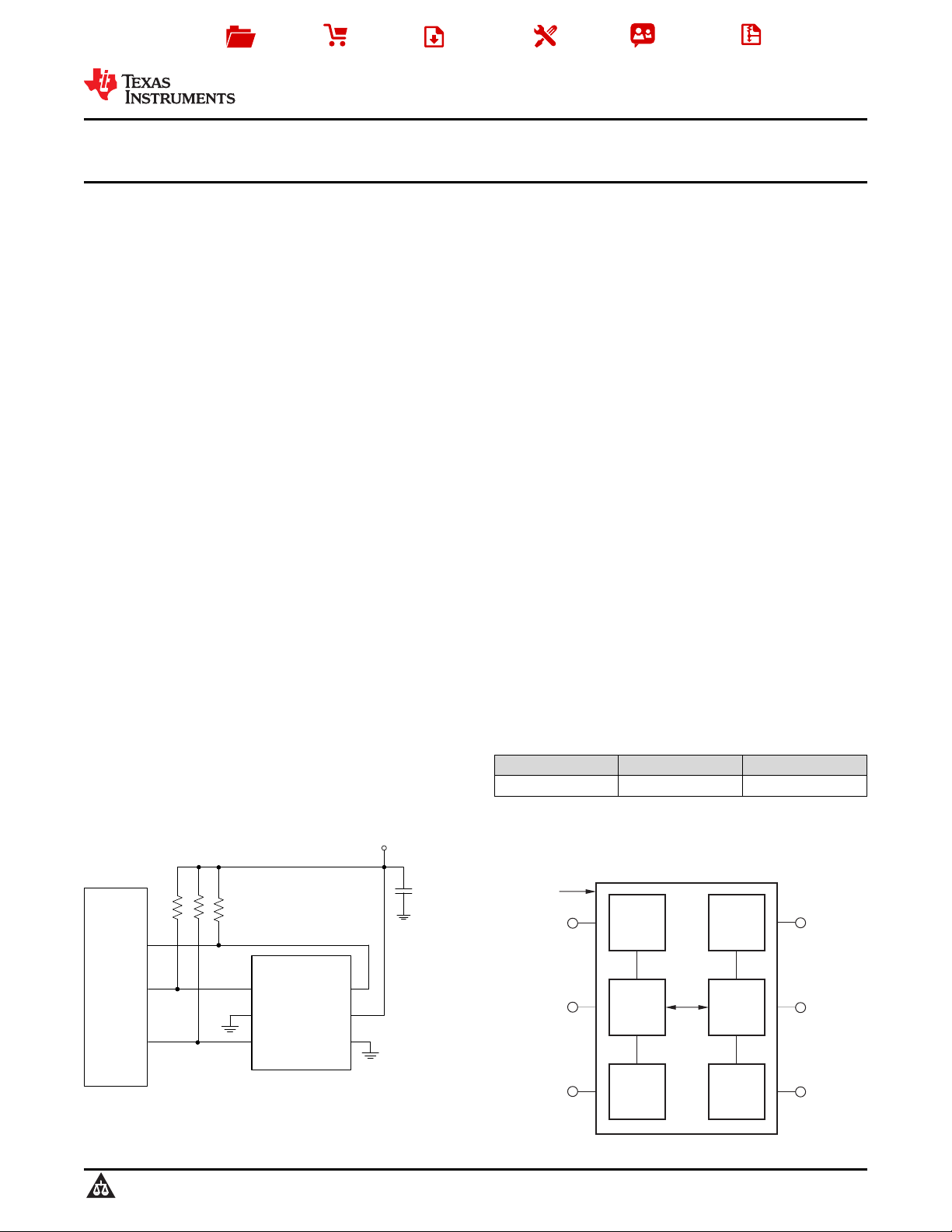
Simplified Schematic
The TMP102 device is a digital temperature sensor
ideal for NTC/PTC thermistor replacement where high
accuracy is required. The device offers an accuracy
of ±0.5°C without requiring calibration or external
component signal conditioning. Device temperature
sensors are highly linear and do not require complex
calculations or lookup tables to derive the
temperature. The on-chip 12-bit ADC offers
resolutions down to 0.0625°C.
The 1.6-mm × 1.6-mm SOT563 package is 68%
smaller footprint than an SOT-23 package. The
TMP102 device features SMBus™, two-wire and I2C
interface compatibility, and allows up to four devices
on one bus. The device also features an SMBus alert
function. The device is specified to operate over
supply voltages from 1.4 to 3.6 V with the maximum
quiescent current of 10 µA over the full operating
range.
The TMP102 device is ideal for extended temperature
measurement in a variety of communication,
computer, consumer, environmental, industrial, and
instrumentation applications. The device is specified
for operation over a temperature range of –40°C to
125°C.
The TMP102 production units are 100% tested
against sensors that are NIST-traceable and are
verified with equipment that are NIST-traceable
through ISO/IEC 17025 accredited calibrations.
Device Information
PART NUMBER PACKAGE BODY SIZE (NOM)
TMP102 SOT563 (6) 1.60 mm × 1.20 mm
(1) For all available packages, see the orderable addendum at
the end of the data sheet.
(1)
TMP102
1
An IMPORTANT NOTICE at the end of this data sheet addresses availability, warranty, changes, use in safety-critical applications,
intellectual property matters and other important disclaimers. PRODUCTION DATA.
Block Diagram
Page 2

TMP102
SBOS397F –AUGUST 2007–REVISED DECEMBER 2015
www.ti.com
Table of Contents
1 Features.................................................................. 1
2 Applications ........................................................... 1
3 Description ............................................................. 1
4 Revision History..................................................... 2
5 Pin Configuration and Functions......................... 3
6 Specifications......................................................... 3
6.1 Absolute Maximum Ratings ..................................... 3
6.2 Handling Ratings....................................................... 3
6.3 Recommended Operating Conditions....................... 4
6.4 Thermal Information.................................................. 4
6.5 Electrical Characteristics........................................... 4
6.6 Timing Requirements ............................................... 5
6.7 Typical Characteristics.............................................. 6
7 Detailed Description .............................................. 7
7.1 Overview................................................................... 7
7.2 Functional Block Diagram ......................................... 7
7.3 Feature Description................................................... 7
7.4 Device Functional Modes........................................ 13
7.5 Programming........................................................... 14
8 Application and Implementation........................ 20
8.1 Application Information............................................ 20
8.2 Typical Application .................................................. 20
9 Power Supply Recommendations...................... 22
10 Layout................................................................... 22
10.1 Layout Guidelines................................................. 22
10.2 Layout Example.................................................... 22
11 Device and Documentation Support................. 23
11.1 Documentation Support ....................................... 23
11.2 Community Resources.......................................... 23
11.3 Trademarks........................................................... 23
11.4 Electrostatic Discharge Caution............................ 23
11.5 Glossary................................................................ 23
12 Mechanical, Packaging, and Orderable
Information........................................................... 23
4 Revision History
NOTE: Page numbers for previous revisions may differ from page numbers in the current version.
Changes from Revision E (April 2015) to Revision F Page
• Added TI Design .................................................................................................................................................................... 1
• Added NIST Features bullet .................................................................................................................................................. 1
• Added last paragraph of Description section ......................................................................................................................... 1
Changes from Revision D (December 2014) to Revision E Page
• Changed the MAX value for the Supply voltage from 3.6 to 4 in the Absolute Maximum Ratings table............................... 3
• Changed MIN, TYP, and MAX values for the Temperature Accuracy (temperature error) parameter.................................. 4
• Changed the frequency from 2.85 to 3.4 MHz in the POWER SUPPLY section of the Electrical Characteristics table ....... 5
• Changed the Temperature Error vs Temperature graph in the Typical Characteristics section............................................ 6
• Changed the Temperature Error at 25°C graph in the Typical Characteristics section......................................................... 6
Changes from Revision C (October 2012) to Revision D Page
• Added Handling Rating table, Feature Description section, Device Functional Modes, Application and
Implementation section, Power Supply Recommendations section, Layout section, Device and Documentation
Support section, and Mechanical, Packaging, and Orderable Information section ............................................................... 3
• Changed parameters in Timing Requirements ...................................................................................................................... 5
Changes from Revision B (October 2008) to Revision C Page
• Changed values for Data Hold Time parameter in Timing Requirements .......................................................................... 11
2 Submit Documentation Feedback Copyright © 2007–2015, Texas Instruments Incorporated
Product Folder Links: TMP102
Page 3
1
2
3
6
5
4
SDA
V+
ADD0
SCL
GND
ALERT
CBZ
www.ti.com
SBOS397F –AUGUST 2007–REVISED DECEMBER 2015
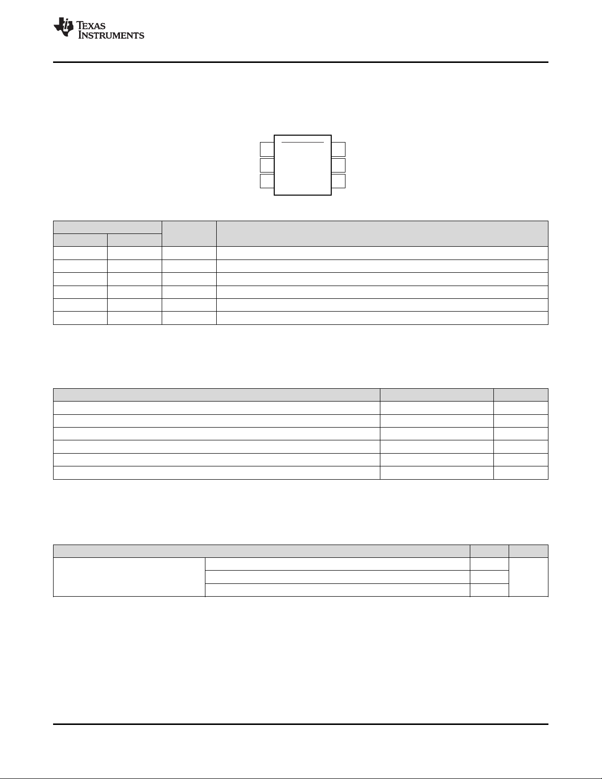
5 Pin Configuration and Functions
DRL Package
6-Pin SOT563
Top View
Pin Functions
PIN
NO. NAME
1 SCL I Serial clock. Open-drain output; requires a pullup resistor.
2 GND — Ground
3 ALERT O Overtemperature alert. Open-drain output; requires a pullup resistor.
4 ADD0 I Address select. Connect to GND or V+
5 V+ I Supply voltage, 1.4 V to 3.6 V
6 SDA I/O Serial data. Open-drain output; requires a pullup resistor.
I/O DESCRIPTION
TMP102
6 Specifications
6.1 Absolute Maximum Ratings
over operating free-air temperature range (unless otherwise noted)
Supply Voltage 4 V
Input Voltage
Output voltage 3.6 V
Operating temperature –55 150 °C
Junction temperature 150 °C
Storage temperature, T
(1) Stresses above these ratings may cause permanent damage. Exposure to absolute maximum conditions for extended periods may
degrade device reliability. These are stress ratings only, and functional operation of the device at these or any other conditions beyond
those specified is not supported.
(2) Input voltage rating applies to all TMP102 input voltages.
(2)
stg
6.2 Handling Ratings
Human-body model (HBM), per ANSI/ESDA/JEDEC JS-001
V
(ESD)
(1) Level listed above is the passing level per ANSI, ESDA, and JEDEC JS-001. JEDEC document JEP155 states that 500-V HBM allows
(2) Level listed above is the passing level per EIA-JEDEC JESD22-C101. JEDEC document JEP157 states that 250-V CDM allows safe
Electrostatic discharge Charged-device model (CDM), per JEDEC specification JESD22-C101
Machine model (MM) ±200
safe manufacturing with a standard ESD control process.
manufacturing with a standard ESD control process.
(1)
MIN MAX UNIT
–0.5 3.6 V
–60 150 °C
VALUE UNIT
(1)
(2)
±2000
±1000 V
Copyright © 2007–2015, Texas Instruments Incorporated Submit Documentation Feedback 3
Product Folder Links: TMP102
Page 4
TMP102
SBOS397F –AUGUST 2007–REVISED DECEMBER 2015
www.ti.com
6.3 Recommended Operating Conditions
over operating free-air temperature range (unless otherwise noted)
MIN NOM MAX UNIT
V+ Supply voltage 1.4 3.3 3.6 V
T
A
Operating free-air temperature –40 125 °C
6.4 Thermal Information
TMP102
THERMAL METRIC
(1)
DRL (SOT563) UNIT
6 PINS
R
θJA
R
θJC(top)
R
θJB
ψ
JT
ψ
JB
Junction-to-ambient thermal resistance 200 °C/W
Junction-to-case (top) thermal resistance 73.7 °C/W
Junction-to-board thermal resistance 34.4 °C/W
Junction-to-top characterization parameter 3.1 °C/W
Junction-to-board characterization parameter 34.2 °C/W
(1) For more information about traditional and new thermal metrics, see the IC Package Thermal Metrics application report, SPRA953.
6.5 Electrical Characteristics
At TA= 25°C and VS= 1.4 to 3.6 V, unless otherwise noted.
PARAMETER TEST CONDITIONS MIN TYP MAX UNIT
TEMPERATURE INPUT
Range –40 125 °C
Accuracy (temperature error) °C
vs supply 0.2 0.5 °C/V
Resolution 0.0625 °C
DIGITAL INPUT/OUTPUT
Input capacitance 3 pF
V
V
I
IN
V
Input logic high 0.7 × (V+) 3.6 V
IH
Input logic low –0.5 0.3 × (V+) V
IL
Input current 0 < VIN< 3.6 V 1 μA
Output logic V
OL
Resolution 12 Bit
Conversion time 26 35 ms
Conversion modes Conv/s
Timeout time 30 40 ms
SDA
ALERT
–25°C to 85°C ±0.5 ±2
–40°C to 125°C ±1 ±3
V+ > 2 V, IOL= 3 mA 0 0.4
V+ < 2 V, IOL= 3 mA 0 0.2 × (V+)
V+ > 2 V, IOL= 3 mA 0 0.4
V+ < 2 V, IOL= 3 mA 0 0.2 × (V+)
CR1 = 0, CR0 = 0 0.25
CR1 = 0, CR0 = 1 1
CR1 = 1, CR0 = 0 (default) 4
CR1 = 1, CR0 = 1 8
4 Submit Documentation Feedback Copyright © 2007–2015, Texas Instruments Incorporated
Product Folder Links: TMP102
Page 5
www.ti.com
Electrical Characteristics (continued)
At TA= 25°C and VS= 1.4 to 3.6 V, unless otherwise noted.
PARAMETER TEST CONDITIONS MIN TYP MAX UNIT
POWER SUPPLY
Operating supply range +1.4 +3.6 V
Serial bus inactive, CR1 = 1, CR0 =
0 (default)
I
Q
I
SD
Average quiescent current 15 μA
Shutdown current 400 kHz μA
TEMPERATURE
Specified range –40 125 °C
Operating range –55 150 °C
Serial bus active, SCL frequency =
400 kHz
Serial bus active, SCL frequency =
3.4 MHz
Serial bus inactive 0.5 1
Serial bus active, SCL frequency =
Serial bus active, SCL frequency =
3.4 MHz
6.6 Timing Requirements
See the Timing Diagrams section for additional information.
ƒ
(SCL)
t
(BUF)
t
(HDSTA)
t
(SUSTA)
t
(SUSTO)
t
(HDDAT)
t
(SUDAT)
t
(LOW)
t
(HIGH)
t
FD
t
RD
t
FC
t
RC
SCL operating frequency V+ 0.001 0.4 0.001 2.85 MHz
Bus-free time between STOP and
START condition
Hold time after repeated START
condition.
After this period, the first clock is
generated.
See Figure 7
repeated start condition setup time 600 160 ns
STOP condition setup time 600 160 ns
Data hold time 100 900 25 105 ns
Data setup time 100 25 ns
SCL-clock low period V+ , see Figure 7 1300 210 ns
SCL-clock high period See Figure 7 600 60 ns
Data fall time See Figure 7 300 80 ns
See Figure 7 300 ns
Data rise time
SCLK ≤ 100 kHz,
see Figure 7
Clock fall time See Figure 7 300 40 ns
Clock rise time See Figure 7 300 40 ns
TMP102
SBOS397F –AUGUST 2007–REVISED DECEMBER 2015
7 10
85
10
80
FAST MODE HIGH-SPEED MODE
MIN TYP MAX MIN TYP MAX
600 160 ns
600 160 ns
1000 ns
UNIT
Copyright © 2007–2015, Texas Instruments Incorporated Submit Documentation Feedback 5
Product Folder Links: TMP102
Page 6
Temperature (qC)
Temperature Error (qC)
-60 -40 -20 0 20 40 60 80 100 120 140
-1
-0.8
-0.6
-0.4
-0.2
0
0.2
0.4
0.6
0.8
1
D002
Mean
Mean + 3 V
Mean 3 V
Temperature Error (qC)
Population
-0.35
-0.3
-0.25
-0.2
-0.15
-0.1
-0.05
0
0.05
0.1
0.15
0.2
0.25
0.3
0.35
0.4
0
10
20
30
40
50
60
70
D001
40
38
36
34
32
30
28
26
24
22
20
Temperature (°C)
-60 -20 40 60 140 160
Conversion Time (ms)
3.6 V Supply
1.4 V Supply
-40 200 80 100 120
100
90
80
70
60
50
40
30
20
10
0
Bus Frequency (Hz)
1k 10k 100k 1M 10M
I ( A)
Q
μ
-55 °C
+25 °C
+125 °C
10
9
8
7
6
5
4
3
2
1
0
Temperature (°C)
-60 -40 0 40 140 160
I ( A)
SD
μ
3.6 V Supply
1.4 V Supply
-20 20 60 80 100 120
20
18
16
14
12
10
8
6
4
2
0
Temperature (°C)
-60 -20 40 60 140 160
I ( A)
Q
μ
3.6 V Supply
-40 0 20 80 100 120
1.4 V Supply
TMP102
SBOS397F –AUGUST 2007–REVISED DECEMBER 2015
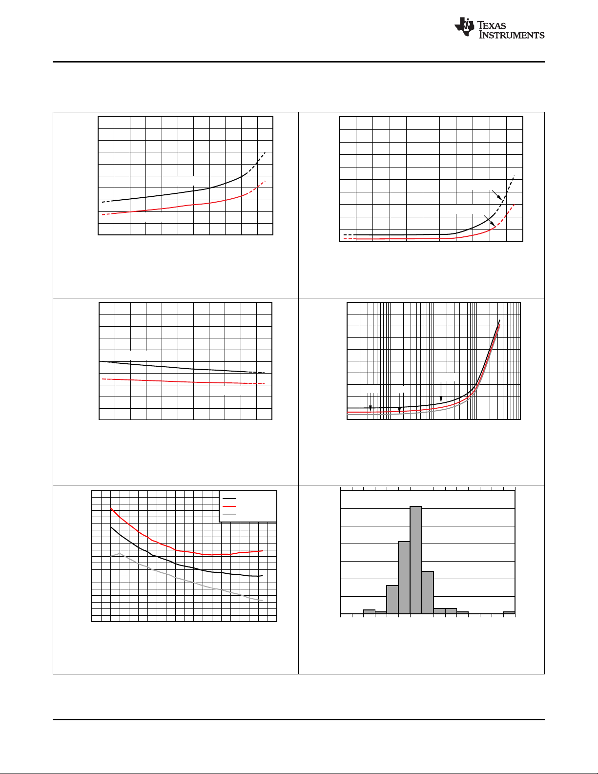
6.7 Typical Characteristics
At TA= 25°C and V+ = 3.3 V, unless otherwise noted.
Four conversions per second
www.ti.com
Figure 1. Average Quiescent Current vs Temperature
Figure 2. Shutdown Current vs Temperature
Figure 3. Conversion Time vs Temperature Figure 4. Quiescent Current vs Bus Frequency
(Temperature at 3.3-V Supply)
6 Submit Documentation Feedback Copyright © 2007–2015, Texas Instruments Incorporated
Figure 5. Temperature Error vs Temperature
Figure 6. Temperature Error at 25°C
Product Folder Links: TMP102
Page 7
Diode
Temp.
Sensor
DS
A/D
Converter
OSC
Control
Logic
Serial
Interface
Config.
andTemp.
Register
Temperature
SCL
1
3
6
4
ALERT
SDA
GND
2 5
V+
ADD0
TMP102
www.ti.com
SBOS397F –AUGUST 2007–REVISED DECEMBER 2015
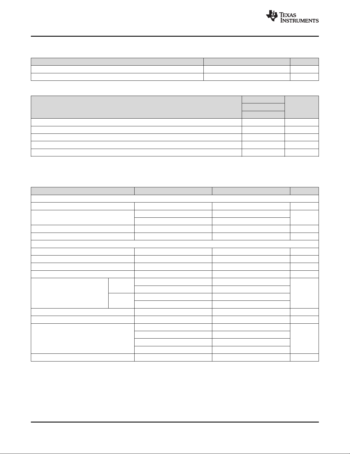
7 Detailed Description
7.1 Overview
The TMP102 device is a digital temperature sensor that is optimal for thermal-management and thermalprotection applications. The TMP102 device is two-wire, SMBus and I2C interface-compatible. The device is
specified over an operating temperature range of –40°C to 125°C. See Functional Block Diagram for a block
diagram of the TMP102 device.
The temperature sensor in the TMP102 device is the chip itself. Thermal paths run through the package leads as
well as the plastic package. The package leads provide the primary thermal path because of the lower thermal
resistance of the metal.
An alternative version of the TMP102 device is available. The TMP112 device has highest accuracy, the same
micro-package, and is pin-to-pin compatible.
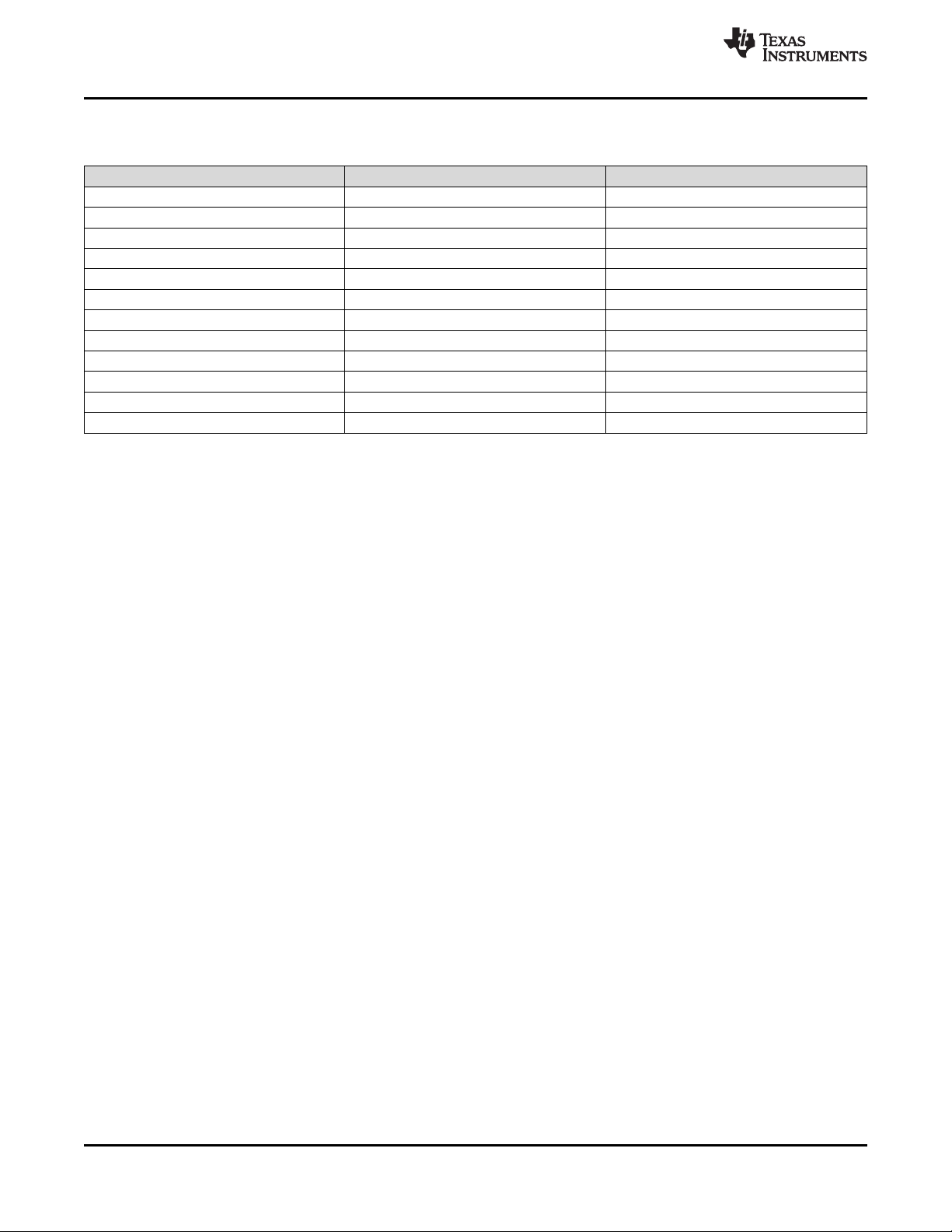
Table 1. Advantages of TMP112 versus TMP102
DEVICE PACKAGE VOLTAGE VOLTAGE RESOLUTION CALIBRATION
TMP112 10 µA 1.4 V 3.6 V Yes
TMP102 10 µA 1.4 V 3.6 V No
COMPATIBLE SUPPLY LOCAL SENSOR ACCURACY
INTERFACES CURRENT (MAX)
I2C
SMBus
I2C
SMBus
SOT563 12 bit 0.5°C: (0°C to 65°C)
1.2 × 1.6 × 0.6 0.0625°C 1°C: (-40°C to 125°C)
SOT563 12 bit 2°C: (25°C to 85°C)
1.2 × 1.6 × 0.6 0.0625°C 3°C: (-40°C to 125°C)
SUPPLY SUPPLY SPECIFIED
(MIN) (MAX) DRIFT SLOPE
7.2 Functional Block Diagram
7.3 Feature Description
7.3.1 Digital Temperature Output
The digital output from each temperature measurement is stored in the read-only temperature register. The
temperature register of the TMP102 device is configured as a 12-bit, read-only register (configuration register EM
bit = 0, see the Extended Mode (EM) section), or as a 13-bit, read-only register (configuration register EM bit = 1)
that stores the output of the most recent conversion. Two bytes must be read to obtain data and are listed in
Table 8 and Table 9. Byte 1 is the most significant byte (MSB), followed by byte 2, the least significant byte
(LSB). The first 12 bits (13 bits in extended mode) are used to indicate temperature. The least significant byte
does not have to be read if that information is not needed. The data format for temperature is summarized in
Table 2 and Table 3. One LSB equals 0.0625°C. Negative numbers are represented in binary twos-complement
format. Following power-up or reset, the temperature register reads 0°C until the first conversion is complete. Bit
D0 of byte 2 indicates normal mode (EM bit = 0) or extended mode (EM bit = 1) , and can be used to distinguish
between the two temperature register data formats. The unused bits in the temperature register always read 0.
Copyright © 2007–2015, Texas Instruments Incorporated Submit Documentation Feedback 7
Product Folder Links: TMP102
Page 8
TMP102
SBOS397F –AUGUST 2007–REVISED DECEMBER 2015
www.ti.com
Feature Description (continued)
Table 2. 12-Bit Temperature Data Format
TEMPERATURE (°C) DIGITAL OUTPUT (BINARY) HEX
128 0111 1111 1111 7FF
127.9375 0111 1111 1111 7FF
100 0110 0100 0000 640
80 0101 0000 0000 500
75 0100 1011 0000 4B0
50 0011 0010 0000 320
25 0001 1001 0000 190
0.25 0000 0000 0100 004
0 0000 0000 0000 000
–0.25 1111 1111 1100 FFC
–25 1110 0111 0000 E70
–55 1100 1001 0000 C90
(1) The resolution for the Temp ADC in Internal Temperature mode is 0.0625°C/count.
Table 2 does not list all temperatures. Use the following rules to obtain the digital data format for a given
temperature or the temperature for a given digital data format.
To convert positive temperatures to a digital data format:
1. Divide the temperature by the resolution
2. Convert the result to binary code with a 12-bit, left-justified format, and MSB = 0 to denote a positive sign.
Example: (50°C) / (0.0625°C / LSB) = 800 = 320h = 0011 0010 0000
To convert a positive digital data format to temperature:
1. Convert the 12-bit, left-justified binary temperature result, with the MSB = 0 to denote a positive sign, to a
decimal number.
2. Multiply the decimal number by the resolution to obtain the positive temperature.
Example: 0011 0010 0000 = 320h = 800 × (0.0625°C / LSB) = 50°C
To convert negative temperatures to a digital data format:
1. Divide the absolute value of the temperature by the resolution, and convert the result to binary code with a
12-bit, left-justified format.
2. Generate the twos complement of the result by complementing the binary number and adding one. Denote a
negative number with MSB = 1.
Example: (|–25°C|) / (0.0625°C / LSB) = 400 = 190h = 0001 1001 0000
Two's complement format: 1110 0110 1111 + 1 = 1110 0111 0000
To convert a negative digital data format to temperature:
1. Generate the twos compliment of the 12-bit, left-justified binary number of the temperature result (with MSB
= 1, denoting negative temperature result) by complementing the binary number and adding one. This
represents the binary number of the absolute value of the temperature.
2. Convert to decimal number and multiply by the resolution to get the absolute temperature, then multiply by
–1 for the negative sign.
Example: 1110 0111 0000 has twos compliment of 0001 1001 0000 = 0001 1000 1111 + 1
Convert to temperature: 0001 1001 0000 = 190h = 400; 400 × (0.0625°C / LSB) = 25°C = (|–25°C|);
(|–25°C|) × (–1) = –25°C
(1)
8 Submit Documentation Feedback Copyright © 2007–2015, Texas Instruments Incorporated
Product Folder Links: TMP102
Page 9
TMP102
www.ti.com
SBOS397F –AUGUST 2007–REVISED DECEMBER 2015
Table 3. 13-Bit Temperature Data Format
TEMPERATURE (°C) DIGITAL OUTPUT (BINARY) HEX
150 0 1001 0110 0000 0960
128 0 1000 0000 0000 0800
127.9375 0 0111 1111 1111 07FF
100 0 0110 0100 0000 0640
80 0 0101 0000 0000 0500
75 0 0100 1011 0000 04B0
50 0 0011 0010 0000 0320
25 0 0001 1001 0000 0190
0.25 0 0000 0000 0100 0004
0 0 0000 0000 0000 0000
–0.25 1 1111 1111 1100 1FFC
–25 1 1110 0111 0000 1E70
–55 1 1100 1001 0000 1C90
7.3.2 Serial Interface
The TMP102 device operates as a slave device only on the two-wire bus and SMBus. Connections to the bus
are made through the open-drain I/O lines, SDA and SCL. The SDA and SCL pins feature integrated spike
suppression filters and Schmitt triggers to minimize the effects of input spikes and bus noise. The TMP102
device supports the transmission protocol for both fast (1 kHz to 400 kHz) and high-speed (1 kHz to 2.85 MHz)
modes. All data bytes are transmitted MSB first.
7.3.3 Bus Overview
The device that initiates the transfer is called a master, and the devices controlled by the master are called
slaves. The bus must be controlled by a master device that generates the serial clock (SCL), controls the bus
access, and generates the START and STOP conditions.
To address a specific device, a START condition is initiated, indicated by pulling the data-line (SDA) from a high
to low logic level when SCL is high. All slaves on the bus shift in the slave address byte on the rising edge of the
clock, with the last bit indicating whether a read or write operation is intended. During the ninth clock pulse, the
slave being addressed responds to the master by generating an acknowledge and by pulling SDA pin low.
A data transfer is then initiated and sent over eight clock pulses followed by an acknowledge bit. During the data
transfer the SDA pin must remain stable when SCL is high, because any change in SDA pin when SCL pin is
high is interpreted as a START signal or STOP signal.
When all data have been transferred, the master generates a STOP condition indicated by pulling SDA pin from
low to high, when the SCL pin is high.
7.3.4 Serial Bus Address
To communicate with the TMP102, the master must first address slave devices via a slave address byte. The
slave address byte consists of seven address bits, and a direction bit indicating the intent of executing a read or
write operation.
The TMP102 features an address pin to allow up to four devices to be addressed on a single bus. Table 4
describes the pin logic levels used to properly connect up to four devices.
Copyright © 2007–2015, Texas Instruments Incorporated Submit Documentation Feedback 9
Product Folder Links: TMP102
Page 10

TMP102
SBOS397F –AUGUST 2007–REVISED DECEMBER 2015
www.ti.com
Table 4. Address Pin and Slave Addresses
DEVICE TWO-WIRE ADDRESS A0 PIN CONNECTION
1001000 Ground
1001001 V+
1001010 SDA
1001011 SCL
7.3.5 Writing and Reading Operation
Accessing a particular register on the TMP102 device is accomplished by writing the appropriate value to the
pointer register. The value for the pointer register is the first byte transferred after the slave address byte with the
R/W bit low. Every write operation to the TMP102 device requires a value for the pointer register (see Figure 8).
When reading from the TMP102 device, the last value stored in the pointer register by a write operation
determines which register is read by a read operation. To change the register pointer for a read operation, a new
value must be written to the pointer register. This action is accomplished by issuing a slave address byte with the
R/W bit low, followed by the pointer register byte. No additional data are required. The master then generates a
START condition and sends the slave address byte with the R/W bit high to initiate the read command. See
Figure 7 for details of this sequence. If repeated reads from the same register are desired, continually sending
the Pointer Register bytes is not necessary because the TMP102 remembers the Pointer Register value until it is
changed by the next write operation.
Register bytes are sent with the most significant byte first, followed by the least significant byte.
7.3.6 Slave Mode Operations
The TMP102 can operate as a slave receiver or slave transmitter. As a slave device, the TMP102 never drives
the SCL line.
7.3.6.1 Slave Receiver Mode
The first byte transmitted by the master is the slave address, with the R/W bit low. The TMP102 then
acknowledges reception of a valid address. The next byte transmitted by the master is the pointer register. The
TMP102 then acknowledges reception of the pointer register byte. The next byte or bytes are written to the
register addressed by the pointer register. The TMP102 acknowledges reception of each data byte. The master
can terminate data transfer by generating a START or STOP condition..
7.3.6.2 Slave Transmitter Mode
The first byte transmitted by the master is the slave address, with the R/W bit high. The slave acknowledges
reception of a valid slave address. The next byte is transmitted by the slave and is the most significant byte of
the register indicated by the pointer register. The master acknowledges reception of the data byte. The next byte
transmitted by the slave is the least significant byte. The master acknowledges reception of the data byte. The
master terminates data transfer by generating a Not-Acknowledge on reception of any data byte, or generating a
START or STOP condition.
7.3.7 SMBus Alert Function
The TMP102 device supports the SMBus alert function. When the TMP102 device operates in Interrupt Mode
(TM = 1), the ALERT pin can be connected as an SMBus alert signal. When a master senses that an ALERT
condition is present on the ALERT line, the master sends an SMBus alert command (0001 1001) to the bus. If
the ALERT pin is active, the device acknowledges the SMBus alert command and responds by returning the
slave address on the SDA line. The eighth bit (LSB) of the slave address byte indicates if the ALERT condition
was caused by the temperature exceeding T
temperature is greater than or equal to T
HIGH
or falling below T
HIGH
. For POL = 0, the LSB is low if the
LOW
; this bit is high if the temperature is less than T
. The polarity of
LOW
this bit is inverted if POL = 1. See Figure 10 for details of this sequence.
If multiple devices on the bus respond to the SMBus alert command, arbitration during the slave address portion
of the SMBus alert command determines which device clears the ALERT status. The device with the lowest twowire address wins the arbitration. If the TMP102 device wins the arbitration, its ALERT pin inactivates at the
completion of the SMBus alert command. If the TMP102 device loses the arbitration, its ALERT pin remains
active.
10 Submit Documentation Feedback Copyright © 2007–2015, Texas Instruments Incorporated
Product Folder Links: TMP102
Page 11

SCL
SDA
t
(LOW)
t
RC
t
FC
t
(HDSTA)
t
(HDSTA)
t
(HDDAT)
t
(SUDAT)
t
(HIGH)
t
(SUSTA)
t
(SUSTO)
t
(BUF)
S
S
P
P
t
RD
t
FD
TMP102
www.ti.com
SBOS397F –AUGUST 2007–REVISED DECEMBER 2015
7.3.8 General Call
The TMP102 device responds to a two-wire general call address (000 0000) if the eighth bit is 0. The device
acknowledges the general call address and responds to commands in the second byte. If the second byte is
0000 0110, the TMP102 device internal registers are reset to power-up values. The TMP102 device does not
support the general address acquire command.
7.3.9 High-Speed (HS) Mode
In order for the two-wire bus to operate at frequencies above 400 kHz, the master device must issue an HSMode master code (0000 1xxx) as the first byte after a START condition to switch the bus to high-speed
operation. The TMP102 device does not acknowledge this byte, but switches the input filters on SDA and SCL
and the output filters on SDA to operate in HS-mode, allowing transfers of up to 2.85 MHz. After the HS-Mode
master code has been issued, the master transmits a two-wire slave address to initiate a data transfer operation.
The bus continues to operate in HS-Mode until a STOP condition occurs on the bus. Upon receiving the STOP
condition, the TMP102 device switches the input and output filters back to fast-mode operation..
7.3.10 Timeout Function
The TMP102 device resets the serial interface if SCL is held low for 30 ms (typ) between a start and stop
condition. The TMP102 device releases the SDA line if the SCL pin is pulled low and waits for a start condition
from the host controller. To avoid activating the time-out function, maintaining a communication speed of at least
1 kHz for SCL operating frequency is necessary..
7.3.11 Timing Diagrams
The TMP102 device is two-wire, SMBus, and I2C-interface compatible. Figure 7, Figure 8, Figure 9, and
Figure 10 list the various operations on the TMP102 device. Parameters for Figure 7 are defined in the Timing
Requirements table. The bus definitions are defined as follows:
Acknowledge Each receiving device, when addressed, is obliged to generate an acknowledge bit. A device that
acknowledges must pull down the SDA line during the acknowledge clock pulse in such a way that
the SDA line is stable low during the high period of the Acknowledge clock pulse. Setup and hold
times must be taken into account. On a master receive, the termination of the data transfer can be
signaled by the master generating a not-acknowledge (1) on the last byte that has been transmitted
by the slave.
Bus Idle Both SDA and SCL lines remain high.
Data Transfer The number of data bytes transferred between a START and a STOP condition is not limited and
is determined by the master device. The TMP102 device can also be used for single byte updates.
To update only the MS byte, terminate the communication by issuing a START or STOP
communication on the bus.
Start Data Transfer A change in the state of the SDA line, from high to low, when the SCL line is high, defines a
START condition. Each data transfer is initiated with a START condition.
Stop Data Transfer A change in the state of the SDA line from low to high when the SCL line is high defines a
STOP condition. Each data transfer is terminated with a repeated START or STOP condition.
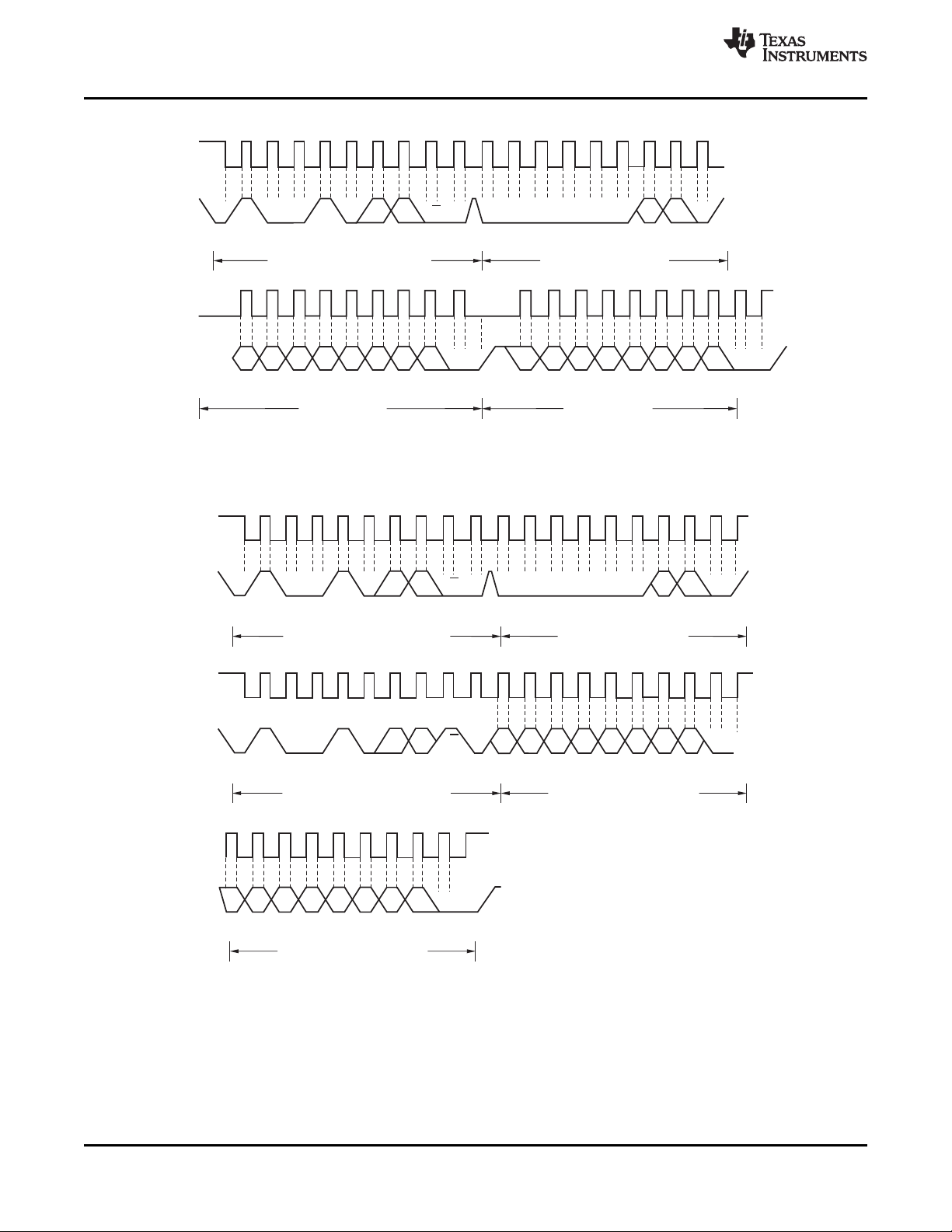
Figure 7. Two-Wire Timing Diagram
Copyright © 2007–2015, Texas Instruments Incorporated Submit Documentation Feedback 11
Product Folder Links: TMP102
Page 12
Frame1Two-WireSlaveAddressByte Frame2PointerRegisterByte
1
StartBy
Master
ACKBy
Device
ACKBy
Device
Frame3Two-WireSlaveAddressByte Frame4DataByte1ReadRegister
StartBy
Master
ACKBy
Device
ACKBy
Master
(2)
From
Device
1 9 1
9
1 9 1
9
SDA
SCL
0 0 1 R/W
0 0 0 0 0 0 P1 P0
¼
¼
¼
SDA
(Continued)
SCL
(Continued)
SDA
(Continued)
SCL
(Continued)
1 0 0 1
0 A1
(1)A0(1)
0
A1
(1)A0(1)
R/W
D7 D6 D5 D4 D3 D2 D1 D0
Frame5DataByte2ReadRegister
StopBy
Master
ACKBy
Master
(3)
From
Device
1
9
D7 D6 D5 D4 D3 D2 D1 D0
StopBy
Master
NOTE: (1)ThevalueofA0andA1aredeterminedbytheADD0pin.
(2)MastershouldleaveSDAhightoterminateasingle-bytereadoperation.
(3)MastershouldleaveSDAhightoterminateatwo-bytereadoperation.
Frame1Two-WireSlaveAddressByte
Frame2PointerRegisterByte
Frame4DataByte2
1
StartBy
Master
ACKBy
Device
ACKBy
Device
ACKBy
Device
StopBy
Master
1 9 1
1
D7 D6 D5 D4 D3 D2 D1 D0
9
Frame3DataByte1
ACKBy
Device
1
D7
SDA
(Continued)
SCL
(Continued)
D6 D5 D4 D3 D2 D1 D0
9
9
SDA
SCL
0 0 1 0
A1
(1)A0(1)
R/W
0 0 0 0 0 0 P1 P0 ¼
¼
NOTE:(1)ThevalueofA0andA1aredeterminedbytheADD0pin.
TMP102
SBOS397F –AUGUST 2007–REVISED DECEMBER 2015
Figure 8. Two-Wire Timing Diagram for Write Word Format
www.ti.com
12 Submit Documentation Feedback Copyright © 2007–2015, Texas Instruments Incorporated
Figure 9. Two-Wire Timing Diagram for Read Word Format
Product Folder Links: TMP102
Page 13

Startup Startof
Conversion
Delay
(1)
26ms
26ms
NOTE:(1)ThevalueofA0andA1aredeterminedbytheADD0pin.
Frame1SMBusALERTResponseAddressByte Frame2SlaveAddressFrom Device
StartBy
Master
ACKBy
Device
From
Device
NACKBy
Master
StopBy
Master
1 9 1
9
SDA
SCL
ALERT
0 0 0 1 1 0 0 R/W
1 0 0 1 A1 A0
Status
TMP102
www.ti.com
SBOS397F –AUGUST 2007–REVISED DECEMBER 2015
Figure 10. Timing Diagram for SMBus Alert
7.4 Device Functional Modes
7.4.1 Continuos-Conversion Mode
The default mode of the TMP102 device is continuos conversion mode. During continuos-conversion mode, the
ADC performs continuos temperature conversions and stores each results to the temperature register,
overwriting the result from the previous conversion. The conversion rate bits, CR1 and CR0, configure the
TMP102 device for conversion rates of 0.25 Hz, 1 Hz, 4 Hz, or 8 Hz. The default rate is 4 Hz. The TMP102
device has a typical conversion time of 26 ms. To achieve different conversion rates, the TMP102 device makes
a conversion and then powers down to wait for the appropriate delay set by CR1 and CR0. Table 5 lists the
settings for CR1 and CR0.
CR1 CR0 CONVERSION RATE
0 0 0.25 Hz
0 1 1 Hz
1 0 4 Hz (default)
1 1 8 Hz
After power-up or general-call reset, the TMP102 immediately starts a conversion, as shown in Figure 11. The
first result is available after 26 ms (typical). The active quiescent current during conversion is 40 μA (typical at
+27°C). The quiescent current during delay is 2.2 μA (typical at +27°C).
(1) Delay is set by CR1 and CR0.
7.4.2 Extended Mode (EM)
The Extended-Mode bit configures the device for Normal mode operation (EM = 0) or Extended mode operation
(EM = 1). In Normal mode, the Temperature Register and high- and low-limit registers use a 12-bit data format.
Normal mode is used to make the TMP102 device compatible with the TMP75 device.
Extended mode (EM = 1) allows measurement of temperatures above 128°C by configuring the Temperature
Register, and high- and low-limit registers for 13-bit data format.
Copyright © 2007–2015, Texas Instruments Incorporated Submit Documentation Feedback 13
Table 5. Conversion Rate Settings
Figure 11. Conversion Start
Product Folder Links: TMP102
Page 14

TMP102
SBOS397F –AUGUST 2007–REVISED DECEMBER 2015
www.ti.com
7.4.3 Shutdown Mode (SD)
The Shutdown-mode bit saves maximum power by shutting down all device circuitry other than the serial
interface, reducing current consumption to typically less than 0.5 μA. Shutdown mode enables when the SD bit is
1; the device shuts down when current conversion is completed. When SD is equal to 0, the device maintains a
continuous conversion state.
7.4.4 One-Shot/Conversion Ready (OS)
The TMP102 device features a one-shot temperature measurement mode. When the device is in Shutdown
Mode, writing a 1 to the OS bit starts a single temperature conversion. During the conversion, the OS bit reads
'0'. The device returns to the shutdown state at the completion of the single conversion. After the conversion, the
OS bit reads 1. This feature reduces power consumption in the TMP102 device when continuous temperature
monitoring is not required.
As a result of the short conversion time, the TMP102 device achieves a higher conversion rate. A single
conversion typically takes 26 ms and a read can take place in less than 20 μs. When using One-Shot Mode, 30
or more conversions per second are possible.
7.4.5 Thermostat Mode (TM)
The thermostat-mode bit indicates to the device whether to operate in comparator mode (TM = 0) or Interrupt
mode (TM = 1).
7.4.5.1 Comparator Mode (TM = 0)
In Comparator mode (TM = 0), the Alert pin is activated when the temperature equals or exceeds the value in the
T
register and remains active until the temperature falls below the value in the T
(HIGH)
register. For more
(LOW)
information on the comparator mode, see the High- and Low-Limit Registers section.
7.4.5.2 Interrupt Mode (TM = 1)
In Interrupt mode (TM = 1), the Alert pin is activated when the temperature exceeds T
or goes below T
(HIGH)
(LOW)
registers. The Alert pin is cleared when the host controller reads the temperature register. For more information
on the interrupt mode, see the High- and Low-Limit Registers section.
7.5 Programming
7.5.1 Pointer Register
Figure 12 illustrates the internal register structure of the TMP102 device. The 8-bit Pointer Register of the device
is used to address a given data register. The Pointer Register uses the two least-significant bytes (LSBs) (see
Table 15 and Table 16) to identify which of the data registers must respond to a read or write command. Table 6
identifies the bits of the Pointer Register byte. During a write command, P2 through P7 must always be '0'.
Table 7 describes the pointer address of the registers available in the TMP102 device. The power-up reset value
of P1 and P0 is 00. By default, the TMP102 device reads the temperature on power up.
14 Submit Documentation Feedback Copyright © 2007–2015, Texas Instruments Incorporated
Product Folder Links: TMP102
Page 15

I/O
Control
Interface
SCL
SDA
Temperature
Register
Configuration
Register
T
LOW
Register
T
HIGH
Register
Pointer
Register
www.ti.com
Programming (continued)
TMP102
SBOS397F –AUGUST 2007–REVISED DECEMBER 2015
Figure 12. Internal Register Structure
Table 6. Pointer Register Byte
P7 P6 P5 P4 P3 P2 P1 P0
0 0 0 0 0 0 Register Bits
Table 7. Pointer Addresses
P1 P0 REGISTER
0 0 Temperature Register (Read Only)
0 1 Configuration Register (Read/Write)
1 0 T
1 1 T
Register (Read/Write)
LOW
Register (Read/Write)
HIGH
7.5.2 Temperature Register
The Temperature Register of the TMP102 is configured as a 12-bit, read-only register (Configuration Register
EM bit = 0, see the Extended Mode section), or as a 13-bit, read-only register (Configuration Register EM bit = 1)
that stores the output of the most recent conversion. Two bytes must be read to obtain data, and are described
in Table 8 and Table 9. Note that byte 1 is the most significant byte, followed by byte 2, the least significant byte.
The first 12 bits (13 bits in Extended mode) are used to indicate temperature. The least significant byte does not
have to be read if that information is not needed.
Table 8. Byte 1 of Temperature Register
D7 D6 D5 D4 D3 D2 D1 D0
T11 T10 T9 T8 T7 T6 T5 T4
(T12) (T11) (T10) (T9) (T8) (T7) (T6) (T5)
(1) Extended mode 13-bit configuration shown in parenthesis.
(1)
Copyright © 2007–2015, Texas Instruments Incorporated Submit Documentation Feedback 15
Product Folder Links: TMP102
Page 16

TMP102
SBOS397F –AUGUST 2007–REVISED DECEMBER 2015
www.ti.com
Table 9. Byte 2 of Temperature Register
D7 D6 D5 D4 D3 D2 D1 D0
T3 T2 T1 T0 0 0 0 0
(T4) (T3) (T2) (T1) (T0) (0) (0) (1)
(1) Extended mode 13-bit configuration shown in parenthesis.
(1)
7.5.3 Configuration Register
The Configuration Register is a 16-bit read/write register used to store bits that control the operational modes of
the temperature sensor. Read/write operations are performed MSB first. Table 10 and Table 11 list the format
and the power-up or reset value of the configuration register. For compatibility, Table 10 and Table 11
correspond to the configuration register in the TMP75 device and TMP275 device (for more information see the
device data sheets, SBOS288 and SBOS363, respectively). All registers are updated byte by byte.
Table 10. Byte 1 of Configuration and Power-Up or Reset Format
D7 D6 D5 D4 D3 D2 D1 D0
OS R1 R0 F1 F0 POL TM SD
0 1 1 0 0 0 0 0
Table 11. Byte 2 of Configuration and Power-Up or Reset Format
D7 D6 D5 D4 D3 D2 D1 D0
CR1 CR0 AL EM 0 0 0 0
1 0 1 0 0 0 0 0
7.5.3.1 Shutdown Mode (SD)
The Shutdown-mode bit saves maximum power by shutting down all device circuitry other than the serial
interface, reducing current consumption to typically less than 0.5 μA. Shutdown mode enables when the SD bit is
1; the device shuts down when current conversion is completed. When SD is equal to 0, the device maintains a
continuous conversion state
7.5.3.2 Thermostat Mode (TM)
The Thermostat mode bit indicates to the device whether to operate in Comparator mode (TM = 0) or Interrupt
mode (TM = 1). For more information on comparator and interrupt modes, see the High- and Low-Limit Registers
section.
7.5.3.3 Polarity (POL)
The polarity bit allows the user to adjust the polarity of the ALERT pin output. If the POL bit is set to 0 (default),
the ALERT pin becomes active low. When the POL bit is set to 1, the ALERT pin becomes active high and the
state of the ALERT pin is inverted. The operation of the ALERT pin in various modes is illustrated in Figure 13.
16 Submit Documentation Feedback Copyright © 2007–2015, Texas Instruments Incorporated
Product Folder Links: TMP102
Page 17

Measured
Temperature
T
HIGH
T
LOW
Device ALERTPIN
(ComparatorMode)
POL=0
Device ALERTPIN
(InterruptMode)
POL=0
Device ALERTPIN
(ComparatorMode)
POL=1
Device ALERTPIN
(InterruptMode)
POL=1
Read Read
Time
Read
www.ti.com
TMP102
SBOS397F –AUGUST 2007–REVISED DECEMBER 2015
Figure 13. Output Transfer Function Diagrams
7.5.3.4 Fault Queue (F1/F0)
A fault condition exists when the measured temperature exceeds the user-defined limits set in the T
T
registers. Additionally, the number of fault conditions required to generate an alert may be programmed
LOW
HIGH
and
using the fault queue. The fault queue is provided to prevent a false alert as a result of environmental noise. The
fault queue requires consecutive fault measurements in order to trigger the alert function. Table 12 defines the
number of measured faults that may be programmed to trigger an alert condition in the device. For T
T
register format and byte order, see the High- and Low-Limit Registers section.
LOW
HIGH
and
Table 12. TMP102 Fault Settings
F1 F0 CONSECUTIVE FAULTS
0 0 1
0 1 2
1 0 4
1 1 6
7.5.3.5 Converter Resolution (R1/R0)
The converter resolution bits, R1 and R0, are read-only bits. The TMP102 converter resolution is set at device
start-up to 11 which sets the temperature register to a 12 bit-resolution.
7.5.3.6 One-Shot (OS)
When the device is in Shutdown Mode, writing a 1 to the OS bit starts a single temperature conversion. During
the conversion, the OS bit reads '0'. The device returns to the shutdown state at the completion of the single
conversion. For more information on the one-shot conversion mode, see the One-Shot/Conversion Ready (OS)
section.
7.5.3.7 EM Bit
The Extended-Mode bit configures the device for Normal Mode operation (EM = 0) or Extended Mode operation
(EM = 1). In normal mode, the temperature register, high-limit register, and low-limit register use a 12-bit data
format. For more information on the extended mode, see the Extended Mode (EM) section.
Copyright © 2007–2015, Texas Instruments Incorporated Submit Documentation Feedback 17
Product Folder Links: TMP102
Page 18

TMP102
SBOS397F –AUGUST 2007–REVISED DECEMBER 2015
www.ti.com
7.5.3.8 Alert (AL Bit)
The AL bit is a read-only function. Reading the AL bit provides information about the comparator mode status.
The state of the POL bit inverts the polarity of data returned from the AL bit. When the POL bit equals 0, the AL
bit reads as 1 until the temperature equals or exceeds T
causing the AL bit to read as 0. The AL bit continues to read as 0 until the temperature falls below T
for the programmed number of consecutive faults,
(HIGH)
(LOW)
for the
programmed number of consecutive faults, when it again reads as 1. The status of the TM bit does not affect the
status of the AL bit..
7.5.3.9 Conversion Rate (CR)
The conversion rate bits, CR1 and CR0, configure the TMP102 device for conversion rates of 0.25 Hz, 1 Hz, 4
Hz, or 8 Hz. The default rate is 4 Hz. For more information on the conversion rate bits, see Table 5.
7.5.4 High- and Low-Limit Registers
The temperature limits are stored in the T
(LOW)
and T
registers in the same format as the temperature result,
(HIGH)
and their values are compared to the temperature result on every conversion. The outcome of the comparison
drives the behavior of the ALERT pin, which operates as a comparator output or an interrupt, and is set by the
TM bit in the configuration register.
In Comparator mode (TM = 0), the ALERT pin becomes active when the temperature equals or exceeds the
value in T
remains active until the temperature falls below the indicated T
and generates a consecutive number of faults according to fault bits F1 and F0. The ALERT pin
HIGH
value for the same number of faults.
LOW
In Interrupt mode (TM = 1), the ALERT pin becomes active when the temperature equals or exceeds the value in
T
for a consecutive number of fault conditions (as shown in Table 5). The ALERT pin remains active until a
HIGH
read operation of any register occurs, or the device successfully responds to the SMBus Alert Response
address. The ALERT pin will also be cleared if the device is placed in Shutdown mode. When the ALERT pin is
cleared, it becomes active again only when temperature falls below T
, and remains active until cleared by a
LOW
read operation of any register or a successful response to the SMBus Alert Response address. When the ALERT
pin is cleared, the above cycle repeats, with the ALERT pin becoming active when the temperature equals or
exceeds T
. The ALERT pin can also be cleared by resetting the device with the General Call Reset
HIGH
command. This action also clears the state of the internal registers in the device, returning the device to
Comparator mode (TM = 0).
Both operational modes are represented in Figure 13. Table 13 through Table 16 describe the format for the
T
and T
HIGH
Power-up reset values for T
and T
LOW
D7 D6 D5 D4 D3 D2 D1 D0
H11 H10 H9 H8 H7 H6 H5 H4
(H12) (H11) (H10) (H9) (H8) (H7) (H6) (H5)
(1) Extended mode 13-bit configuration shown in parenthesis.
D7 D6 D5 D4 D3 D2 D1 D0
H3 H2 H1 H0 0 0 0 0
(H4) (H3) (H2) (H1) (H0) (0) (0) (0)
D7 D6 D5 D4 D3 D2 D1 D0
L11 L10 L9 L8 L7 L6 L5 L4
(L12) (L11) (L10) (L9) (L8) (L7) (L6) (L5)
(1) Extended mode 13-bit configuration shown in parenthesis.
registers. Note that the most significant byte is sent first, followed by the least significant byte.
LOW
HIGH
and T
LOW
are: T
= +80°C and T
HIGH
= +75°C. The format of the data for T
LOW
is the same as for the Temperature Register.
Table 13. Byte 1 Temperature Register
Table 14. Byte 2 Temperature Register
Table 15. Byte 1 Temperature Register
HIGH
HIGH
LOW
(1)
(1)
HIGH
18 Submit Documentation Feedback Copyright © 2007–2015, Texas Instruments Incorporated
Product Folder Links: TMP102
Page 19

www.ti.com
TMP102
SBOS397F –AUGUST 2007–REVISED DECEMBER 2015
Table 16. Byte 2 Temperature Register
D7 D6 D5 D4 D3 D2 D1 D0
L3 L2 L1 L0 0 0 0 0
(L4) (L3) (L2) (L1) (L0) (0) (0) (0)
LOW
Copyright © 2007–2015, Texas Instruments Incorporated Submit Documentation Feedback 19
Product Folder Links: TMP102
Page 20
SCL
GND
ALERT
2
4
1
ADD0
V+
6
3
5
0.01 µF
Two-Wire
Host Controller
TMP102
1.4 V to 3.6 V
SDA
Pullup Resistors
Supply Bypass
Capacitor
Supply Voltage
5 k
TMP102
SBOS397F –AUGUST 2007–REVISED DECEMBER 2015
www.ti.com
8 Application and Implementation
NOTE
Information in the following applications sections is not part of the TI component
specification, and TI does not warrant its accuracy or completeness. TI’s customers are
responsible for determining suitability of components for their purposes. Customers should
validate and test their design implementation to confirm system functionality.
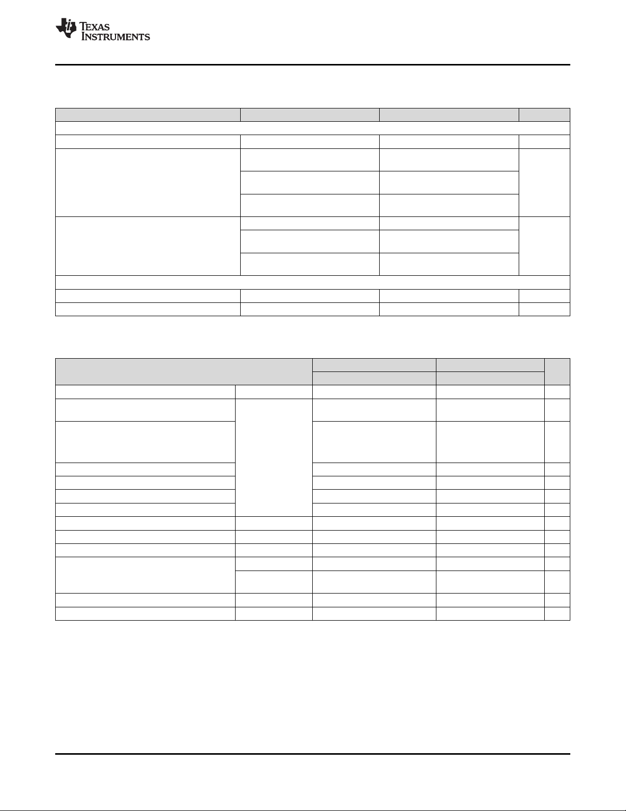
8.1 Application Information
The TMP102 device is used to measure the PCB temperature of the board location where the device is mounted.
The programmable address options allow up to four locations on the board to be monitored on a single serial
bus.
8.2 Typical Application
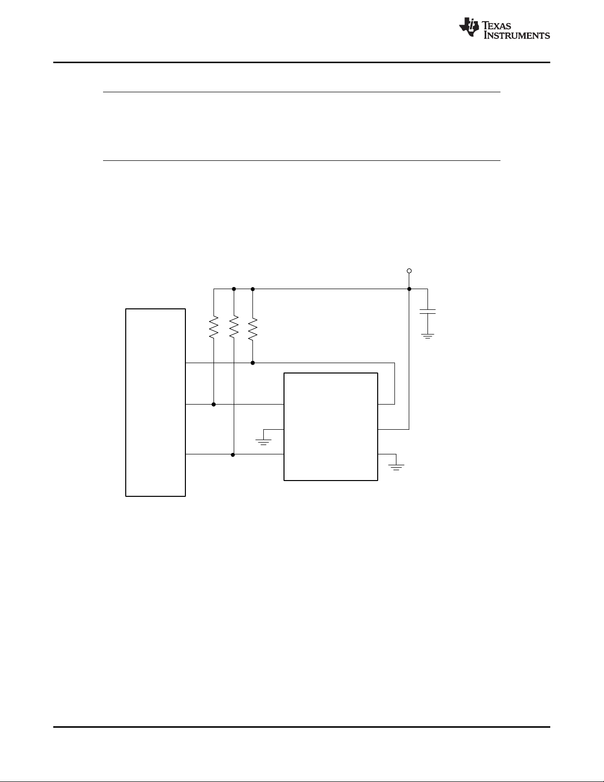
Figure 14. Typical Connections
8.2.1 Design Requirements
The TMP102 device requires pullup resistors on the SCL, SDA, and ALERT pins. The recommended value for
the pullup resistors is 5-kΩ. In some applications the pullup resistor can be lower or higher than 5 kΩ but must
not exceed 3 mA of current on any of those pins. A 0.01-μF bypass capacitor on the supply is recommended as
shown in Figure 14. The SCL and SDA lines can be pulled up to a supply that is equal to or higher than V+
through the pullup resistors. To configure one of four different addresses on the bus, connect the ADD0 pin to
either the GND, V+, SDA, or SCL pin.
8.2.2 Detailed Design Procedure
Place the TMP102 device in close proximity to the heat source that must be monitored, with a proper layout for
good thermal coupling. This placement ensures that temperature changes are captured within the shortest
possible time interval. To maintain accuracy in applications that require air or surface temperature measurement,
care must be taken to isolate the package and leads from ambient air temperature. A thermally-conductive
adhesive is helpful in achieving accurate surface temperature measurement.
20 Submit Documentation Feedback Copyright © 2007–2015, Texas Instruments Incorporated
Product Folder Links: TMP102
Page 21

Time (s)
Temperature (qC)
-1 1 3 5 7 9 11 13 15 17 19
25
30
35
40
45
50
55
60
65
70
75
80
85
90
95
100
Device
SCL SDA
GND V+
ALERT ADD0
C
(F)
10 nF≥
R
(F)
5 k≤ Ω
Supply Voltage
TMP102
www.ti.com
SBOS397F –AUGUST 2007–REVISED DECEMBER 2015
Typical Application (continued)
The TMP102 device is a very low-power device and generates very low noise on the supply bus. Applying an RC
filter to the V+ pin of the TMP102 device can further reduce any noise that the TMP102 device might propagate
to other components. R
8.2.3 Application Curve
Figure 16 shows the step response of the TMP102 device to a submersion in an oil bath of 100ºC from room
temperature (27ºC). The time-constant, or the time for the output to reach 63% of the input step, is 0.8 s. The
time-constant result depends on the printed circuit board (PCB) that the TMP102 device is mounted. For this test,
the TMP102 device was soldered to a two-layer PCB that measured 0.375 inch × 0.437 inch.
space
in Figure 15 must be less than 5 kΩ and C
(F)
Figure 15. Noise Reduction Techniques
must be greater than 10 nF.
(F)
Copyright © 2007–2015, Texas Instruments Incorporated Submit Documentation Feedback 21
Figure 16. Temperature Step Response
Product Folder Links: TMP102
Page 22

Serial Bus Traces
Pullup Resistors
Supply Bypass
Capacitor
Via to Power or
Ground Plane
Via to Internal Layer
Supply Voltage
SCL
GND
ALERT ADD0
V+
SDA
Ground Plane for
Thermal Coupling
to Heat Source
Heat Source
TMP102
SBOS397F –AUGUST 2007–REVISED DECEMBER 2015
www.ti.com
9 Power Supply Recommendations
The TMP102 device operates with power supply in the range of 1.4 to 3.6 V. The device is optimized for
operation at 3.3-V supply but can measure temperature accurately in the full supply range.
A power-supply bypass capacitor is required for proper operation. Place this capacitor as close as possible to the
supply and ground pins of the device. A typical value for this supply bypass capacitor is 0.01 μF. Applications
with noisy or high-impedance power supplies may require additional decoupling capacitors to reject power-supply
noise.
10 Layout
10.1 Layout Guidelines
Place the power-supply bypass capacitor as close as possible to the supply and ground pins. The recommended
value of this bypass capacitor is 0.01 μF. Additional decoupling capacitance can be added to compensate for
noisy or high-impedance power supplies. Pull up the open-drain output pins (SDA , SCL and ALERT) through 5kΩ pullup resistors.
10.2 Layout Example
22 Submit Documentation Feedback Copyright © 2007–2015, Texas Instruments Incorporated
Figure 17. TMP102 Layout Example
Product Folder Links: TMP102
Page 23

TMP102
www.ti.com
SBOS397F –AUGUST 2007–REVISED DECEMBER 2015
11 Device and Documentation Support
11.1 Documentation Support
11.1.1 Related Documentation
For related documentation see the following:
• TMP175, TMP75 Data Sheet, SBOS288
• TMP275 Data Sheet, SBOS363
• Capacitive Touch Operated Automotive LED Dome Light with Haptics Feedback Design Guide
11.2 Community Resources
The following links connect to TI community resources. Linked contents are provided "AS IS" by the respective
contributors. They do not constitute TI specifications and do not necessarily reflect TI's views; see TI's Terms of
Use.
TI E2E™ Online Community TI's Engineer-to-Engineer (E2E) Community. Created to foster collaboration
among engineers. At e2e.ti.com, you can ask questions, share knowledge, explore ideas and help
solve problems with fellow engineers.
Design Support TI's Design Support Quickly find helpful E2E forums along with design support tools and
contact information for technical support.
11.3 Trademarks
E2E is a trademark of Texas Instruments.
SMBus is a trademark of Intel, Inc.
All other trademarks are the property of their respective owners.
11.4 Electrostatic Discharge Caution
These devices have limited built-in ESD protection. The leads should be shorted together or the device placed in conductive foam
during storage or handling to prevent electrostatic damage to the MOS gates.
11.5 Glossary
SLYZ022 — TI Glossary.
This glossary lists and explains terms, acronyms, and definitions.
12 Mechanical, Packaging, and Orderable Information
The following pages include mechanical, packaging, and orderable information. This information is the most
current data available for the designated devices. This data is subject to change without notice and revision of
this document. For browser-based versions of this data sheet, refer to the left-hand navigation.
Copyright © 2007–2015, Texas Instruments Incorporated Submit Documentation Feedback 23
Product Folder Links: TMP102
Page 24

PACKAGE OPTION ADDENDUM
www.ti.com
PACKAGING INFORMATION
Orderable Device Status
TMP102AIDRLR ACTIVE SOT DRL 6 4000 Green (RoHS
TMP102AIDRLRG4 ACTIVE SOT DRL 6 4000 Green (RoHS
TMP102AIDRLT ACTIVE SOT DRL 6 250 Green (RoHS
TMP102AIDRLTG4 ACTIVE SOT DRL 6 250 Green (RoHS
(1)
The marketing status values are defined as follows:
ACTIVE: Product device recommended for new designs.
LIFEBUY: TI has announced that the device will be discontinued, and a lifetime-buy period is in effect.
NRND: Not recommended for new designs. Device is in production to support existing customers, but TI does not recommend using this part in a new design.
PREVIEW: Device has been announced but is not in production. Samples may or may not be available.
OBSOLETE: TI has discontinued the production of the device.
Package Type Package
(1)
Drawing
Pins Package
Qty
Eco Plan
(2)
& no Sb/Br)
& no Sb/Br)
& no Sb/Br)
& no Sb/Br)
Lead/Ball Finish
(6)
CU NIPDAU Level-1-260C-UNLIM -40 to 125 CBZ
CU NIPDAU Level-1-260C-UNLIM -40 to 125 CBZ
CU NIPDAU Level-1-260C-UNLIM -40 to 125 CBZ
CU NIPDAU Level-1-260C-UNLIM -40 to 125 CBZ
MSL Peak Temp
(3)
Op Temp (°C) Device Marking
(4/5)
(2)
Eco Plan - The planned eco-friendly classification: Pb-Free (RoHS), Pb-Free (RoHS Exempt), or Green (RoHS & no Sb/Br) - please check http://www.ti.com/productcontent for the latest availability
information and additional product content details.
TBD: The Pb-Free/Green conversion plan has not been defined.
Pb-Free (RoHS): TI's terms "Lead-Free" or "Pb-Free" mean semiconductor products that are compatible with the current RoHS requirements for all 6 substances, including the requirement that
lead not exceed 0.1% by weight in homogeneous materials. Where designed to be soldered at high temperatures, TI Pb-Free products are suitable for use in specified lead-free processes.
Pb-Free (RoHS Exempt): This component has a RoHS exemption for either 1) lead-based flip-chip solder bumps used between the die and package, or 2) lead-based die adhesive used between
the die and leadframe. The component is otherwise considered Pb-Free (RoHS compatible) as defined above.
Green (RoHS & no Sb/Br): TI defines "Green" to mean Pb-Free (RoHS compatible), and free of Bromine (Br) and Antimony (Sb) based flame retardants (Br or Sb do not exceed 0.1% by weight
in homogeneous material)
(3)
MSL, Peak Temp. - The Moisture Sensitivity Level rating according to the JEDEC industry standard classifications, and peak solder temperature.
(4)
There may be additional marking, which relates to the logo, the lot trace code information, or the environmental category on the device.
(5)
Multiple Device Markings will be inside parentheses. Only one Device Marking contained in parentheses and separated by a "~" will appear on a device. If a line is indented then it is a continuation
of the previous line and the two combined represent the entire Device Marking for that device.
(6)
Lead/Ball Finish - Orderable Devices may have multiple material finish options. Finish options are separated by a vertical ruled line. Lead/Ball Finish values may wrap to two lines if the finish
value exceeds the maximum column width.
8-Dec-2015
Samples
Addendum-Page 1
Page 25

PACKAGE OPTION ADDENDUM
www.ti.com
Important Information and Disclaimer:The information provided on this page represents TI's knowledge and belief as of the date that it is provided. TI bases its knowledge and belief on information
provided by third parties, and makes no representation or warranty as to the accuracy of such information. Efforts are underway to better integrate information from third parties. TI has taken and
continues to take reasonable steps to provide representative and accurate information but may not have conducted destructive testing or chemical analysis on incoming materials and chemicals.
TI and TI suppliers consider certain information to be proprietary, and thus CAS numbers and other limited information may not be available for release.
In no event shall TI's liability arising out of such information exceed the total purchase price of the TI part(s) at issue in this document sold by TI to Customer on an annual basis.
OTHER QUALIFIED VERSIONS OF TMP102 :
Automotive: TMP102-Q1
•
NOTE: Qualified Version Definitions:
Automotive - Q100 devices qualified for high-reliability automotive applications targeting zero defects
•
8-Dec-2015
Addendum-Page 2
Page 26

PACKAGE MATERIALS INFORMATION
www.ti.com 8-Dec-2015
TAPE AND REEL INFORMATION
*All dimensions are nominal
Device Package
Type
TMP102AIDRLR SOT DRL 6 4000 180.0 8.4 1.98 1.78 0.69 4.0 8.0 Q3
TMP102AIDRLT SOT DRL 6 250 180.0 9.5 1.78 1.78 0.69 4.0 8.0 Q3
Package
Drawing
Pins SPQ Reel
Diameter
(mm)
Reel
Width
W1 (mm)
A0
(mm)B0(mm)K0(mm)P1(mm)W(mm)
Pin1
Quadrant
Pack Materials-Page 1
Page 27

PACKAGE MATERIALS INFORMATION
www.ti.com 8-Dec-2015
*All dimensions are nominal
Device Package Type Package Drawing Pins SPQ Length (mm) Width (mm) Height (mm)
TMP102AIDRLR SOT DRL 6 4000 202.0 201.0 28.0
TMP102AIDRLT SOT DRL 6 250 184.0 184.0 19.0
Pack Materials-Page 2
Page 28

Page 29

Page 30

IMPORTANT NOTICE
Texas Instruments Incorporated and its subsidiaries (TI) reserve the right to make corrections, enhancements, improvements and other
changes to its semiconductor products and services per JESD46, latest issue, and to discontinue any product or service per JESD48, latest
issue. Buyers should obtain the latest relevant information before placing orders and should verify that such information is current and
complete. All semiconductor products (also referred to herein as “components”) are sold subject to TI’s terms and conditions of sale
supplied at the time of order acknowledgment.
TI warrants performance of its components to the specifications applicable at the time of sale, in accordance with the warranty in TI’s terms
and conditions of sale of semiconductor products. Testing and other quality control techniques are used to the extent TI deems necessary
to support this warranty. Except where mandated by applicable law, testing of all parameters of each component is not necessarily
performed.
TI assumes no liability for applications assistance or the design of Buyers’ products. Buyers are responsible for their products and
applications using TI components. To minimize the risks associated with Buyers’ products and applications, Buyers should provide
adequate design and operating safeguards.
TI does not warrant or represent that any license, either express or implied, is granted under any patent right, copyright, mask work right, or
other intellectual property right relating to any combination, machine, or process in which TI components or services are used. Information
published by TI regarding third-party products or services does not constitute a license to use such products or services or a warranty or
endorsement thereof. Use of such information may require a license from a third party under the patents or other intellectual property of the
third party, or a license from TI under the patents or other intellectual property of TI.
Reproduction of significant portions of TI information in TI data books or data sheets is permissible only if reproduction is without alteration
and is accompanied by all associated warranties, conditions, limitations, and notices. TI is not responsible or liable for such altered
documentation. Information of third parties may be subject to additional restrictions.
Resale of TI components or services with statements different from or beyond the parameters stated by TI for that component or service
voids all express and any implied warranties for the associated TI component or service and is an unfair and deceptive business practice.
TI is not responsible or liable for any such statements.
Buyer acknowledges and agrees that it is solely responsible for compliance with all legal, regulatory and safety-related requirements
concerning its products, and any use of TI components in its applications, notwithstanding any applications-related information or support
that may be provided by TI. Buyer represents and agrees that it has all the necessary expertise to create and implement safeguards which
anticipate dangerous consequences of failures, monitor failures and their consequences, lessen the likelihood of failures that might cause
harm and take appropriate remedial actions. Buyer will fully indemnify TI and its representatives against any damages arising out of the use
of any TI components in safety-critical applications.
In some cases, TI components may be promoted specifically to facilitate safety-related applications. With such components, TI’s goal is to
help enable customers to design and create their own end-product solutions that meet applicable functional safety standards and
requirements. Nonetheless, such components are subject to these terms.
No TI components are authorized for use in FDA Class III (or similar life-critical medical equipment) unless authorized officers of the parties
have executed a special agreement specifically governing such use.
Only those TI components which TI has specifically designated as military grade or “enhanced plastic” are designed and intended for use in
military/aerospace applications or environments. Buyer acknowledges and agrees that any military or aerospace use of TI components
which have not been so designated is solely at the Buyer's risk, and that Buyer is solely responsible for compliance with all legal and
regulatory requirements in connection with such use.
TI has specifically designated certain components as meeting ISO/TS16949 requirements, mainly for automotive use. In any case of use of
non-designated products, TI will not be responsible for any failure to meet ISO/TS16949.
Products Applications
Audio www.ti.com/audio Automotive and Transportation www.ti.com/automotive
Amplifiers amplifier.ti.com Communications and Telecom www.ti.com/communications
Data Converters dataconverter.ti.com Computers and Peripherals www.ti.com/computers
DLP® Products www.dlp.com Consumer Electronics www.ti.com/consumer-apps
DSP dsp.ti.com Energy and Lighting www.ti.com/energy
Clocks and Timers www.ti.com/clocks Industrial www.ti.com/industrial
Interface interface.ti.com Medical www.ti.com/medical
Logic logic.ti.com Security www.ti.com/security
Power Mgmt power.ti.com Space, Avionics and Defense www.ti.com/space-avionics-defense
Microcontrollers microcontroller.ti.com Video and Imaging www.ti.com/video
RFID www.ti-rfid.com
OMAP Applications Processors www.ti.com/omap TI E2E Community e2e.ti.com
Wireless Connectivity www.ti.com/wirelessconnectivity
Mailing Address: Texas Instruments, Post Office Box 655303, Dallas, Texas 75265
Copyright © 2015, Texas Instruments Incorporated
Page 31

 Loading...