

Page 1
SBOS231G − JANUARY 2002 − REVISED NOVEMBER 2007
Please be aware that an important notice concerning availability, standard warranty, and use in critical applications of Texas Instruments
Digital Temperature Sensor
with I2Ct Interface
TMP100
TMP101
FEATURES
D DIGITAL OUTPUT: I
D RESOLUTION: 9- to 12-Bits, User-Selectable
D ACCURACY:
±2.0°C from −25°C to +85°C (max)
±3.0°C from −55°C to +125°C (max)
D LOW QUIESCENT CURRENT:
45µA, 0.1µA Standby
D WIDE SUPPLY RANGE: 2.7V to 5.5V
D TINY SOT23-6 PACKAGE
2
C Serial 2-Wire
APPLICATIONS
D POWER-SUPPLY TEMPERATURE
MONITORING
D COMPUTER PERIPHERAL THERMAL
PROTECTION
D NOTEBOOK COMPUTERS
D CELL PHONES
D BATTERY MANAGEMENT
D OFFICE MACHINES
D THERMOSTAT CONTROLS
D ENVIRONMENTAL MONITORING AND HVAC
D ELECTROMECHANICAL DEVICE
TEMPERATURE
DESCRIPTION
The TMP100 and TMP101 are two-wire, serial output
temperature sensors available in SOT23-6 packages.
Requiring no external components, the TMP100 and
TMP101 are capable of reading temperatures with a
resolution of 0.0625°C.
The TMP100 and TMP101 feature SMBus and I
interface compatibility, with the TMP100 allowing up to
eight devices on one bus. The TMP101 offers SMBus alert
function with up to three devices per bus.
The TMP100 and TMP101 are ideal for extended
temperature measurement in a variety of communication,
computer, consumer, environmental, industrial, and
instrumentation applications.
The TMP100 and TMP101 are specified for operation over
a temperature range of −55°C to +125°C.
2
C
Temperature
Diode
1
2
3
Temp.
Sensor
∆Σ
A/D
Converter
OSC
TMP100
SCL
GND
ADD1
semiconductor products and disclaimers thereto appears at the end of this data sheet.
I2C is a trademark of NXP Semiconductors. All other trademarks are the property of their respective owners.
! !
Control
Logic
Serial
Interface
Config
and Temp
Register
6
SDA
5
ADD0
4
V+
www.ti.com
Temperature
SCL
GND
ALERT
Diode
1
Tem p.
Sensor
∆Σ
2
A/D
Converter
3
OSC
TMP101
Copyright 2002−2007, Texas Instruments Incorporated
Control
Logic
Serial
Interface
Config
and Temp
Register
6
SDA
5
ADD0
4
V+
Page 2
"#$$
TMP100
SOT23-6
DBV
T100
TMP101
SOT23-6
DBV
T101
"#$#
SBOS231G − JANUARY 2002 − REVISED NOVEMBER 2007
www.ti.com
This integrated circuit can be damaged by ESD. Texas
Instruments recommends that all integrated circuits be
handled with appropriate precautions. Failure to observe
(1)
(1)
−0.5V to 7.5V. . . . . . . . . . . . . . . . . . . . . . . . . . . . . .
proper handling and installation procedures can cause damage.
ESD damage can range from subtle performance degradation to
complete device failure. Precision integrated circuits may be more
susceptible t o damage because very small parametric changes could
cause the device not to meet its published specifications.
ABSOLUTE MAXIMUM RATINGS
Power Supply, V+ 7.5V. . . . . . . . . . . . . . . . . . . . . . . . . . . . . . . . . . . .
Input Voltage
Operating Temperature Range −55°C to +125°C. . . . . . . . . . . . . . .
Storage Temperature Range −60°C to +150°C. . . . . . . . . . . . . . . . .
Junction Temperature (TJ max) +150°C. . . . . . . . . . . . . . . . . . . . . .
ESD Rating, Human Body Model 2000V. . . . . . . . . . . . . . . . . . . . .
(1)
Stresses above these ratings may cause permanent damage.
Exposure to absolute maximum conditions for extended periods
may degrade device reliability. These are stress ratings only , an d
functional operation of the device at these or any other conditions
beyond those specified is not supported.
(2)
Input voltage rating applies to all TMP100 and TMP101 input
voltages.
(2)
Machine Model 200V. . . . . . . . . . . . . . . . . . . . . . .
ORDERING INFORMATION
PRODUCT PACKAGE-LEAD PACKAGE DESIGNATOR PACKAGE MARKING
(1)
For the most current package and ordering information, see the Package Option Addendum at the end of this document, or see the TI web site
at www .ti.com.
PIN CONFIGURATION
Top View SOT23 Top View SOT23
SCL
GND
ADD1
1
2
3
T100
TMP100
SDA
6
5
ADD0
4
V+
SCL
GND
ALERT
1
2
3
T101
TMP101
6
SDA
5
ADD0
4
V+
2
Page 3

"#$$
PARAMETER
TEST CONDITIONS
UNIT
"#$#
www.ti.com
SBOS231G − JANUARY 2002 − REVISED NOVEMBER 2007
ELECTRICAL CHARACTERISTICS
At TA = −55°C to +125°C and V+ = 2.7V to 5.5V, unless otherwise noted.
TMP100, TMP101
MIN TYP MAX
TEMPERATURE INPUT
Range −55 +125 °C
Accuracy (temperature error) −25°C to +85°C ±0.5 ±2.0 °C
−55°C to +125°C ±1.0 ±3.0 °C
Resolution Selectable ±0.0625 °C
DIGIT AL INPUT/OUTPUT
Input Logic Levels:
V
IH
V
IL
Input Current, I
Output Logic Levels:
VOL SDA IOL = 3mA 0 0.15 0.4 V
VOL ALERT IOL = 4mA 0 0.15 0.4 V
Resolution Selectable 9 to 12 Bits
Conversion Time 9-Bit 40 75 ms
Conversion Rate 9-Bit 25 s/s
POWER SUPPLY
Operating Range 2.7 5.5 V
Quiescent Current I
Shutdown Current I
TEMPERATURE RANGE
Specified Range −55 +125 °C
Storage Range −60 +150 °C
Thermal Resistance q
IN
Q
Serial Bus Active, SCL Frequency = 400kHz 70 µA
Serial Bus Active, SCL Frequency = 3.4MHz 150 µA
SD
Serial Bus Active, SCL Frequency = 400kHz 20 µA
Serial Bus Active, SCL Frequency = 3.4MHz 100 µA
JA
0V ≤ VIN ≤ 6V 1 µA
10-Bit 80 150 ms
11-Bit 160 300 ms
12-Bit 320 600 ms
10-Bit 12 s/s
11-Bit 6 s/s
12-Bit 3 s/s
Serial Bus Inactive 45 75 µA
Serial Bus Inactive 0.1 1 µA
SOT23-6 Surface-Mount 200 °C/W
0.7(V+) 6.0 V
−0.5 0.3(V+) V
3
Page 4
"#$$
"#$#
SBOS231G − JANUARY 2002 − REVISED NOVEMBER 2007
TYPICAL CHARACTERISTICS
At TA = +25°C and V+ = 5.0V, unless otherwise noted.
www.ti.com
70
60
A)
µ
50
(
Q
I
40
30
400
350
300
Conversion Time (ms)
250
−60−40−
−60−40−
QUIESCENT CURRENTvs TEMPERATURE
V+=5V
Serial Bus Inactive
200 20406080100120140
Temperature (_C)
CONVERSION TIME vsTEMPERATURE
V+ = 5V
V+ = 2.7V
NOTE: 12−bit resolution.
200 20406080100120140
Temperature (_C)
V+=2.7V
1.0
0.9
0.8
0.7
0.6
A)
0.5
µ
(
0.4
SD
I
0.3
0.2
0.1
0.0
−
0.1
2.0
1.5
C)
1.0
_
0.5
0.0
−
0.5
−
1.0
Temperature Error(
−
1.5
−
2.0
SHUTDOWN CURRENT vs TEMPERATURE
−60−40−
3 Typical Units
−60−40−
20 0 20 40 60 80 100 120 140
Temperature (_C)
TEMPERATURE ACCURACY vs TEMPERATURE
NOTE: 12−bit resoluti on.
20 0 20 40 60 80 100 120 140
Temperature (_C)
QUIESCENT CURRENTWITH
180
160
140
120
100
A)
µ
(
Q
80
I
60
40
20
FAST MODE Hs MODE
0
10k 100k 1M 10M
BUS ACTIVITY vs TEMPERATURE
125_C
25_C
−55_
C
SCL Frequency (Hz)
125_C
−55_
25_C
C
4
Page 5
www.ti.com
"#$$
"#$#
SBOS231G − JANUARY 2002 − REVISED NOVEMBER 2007
APPLICATIONS INFORMATION
The TMP100 and TMP101 are digital temperature sensors
optimal for thermal management and thermal protection
applications. The TMP100 and TMP101 are I2C and
SMBus interface-compatible and are specified over a
temperature range of −55°C to +125°C.
The TMP100 and TMP101 require no external
components for operation except for pull-up resistors on
SCL, SDA, and ALERT, although a 0.1µF bypass
capacitor is recommended, as shown in Figure 1 and
Figure 2.
V+
4
1
SCL
2
To I
Controller
C
SDA
6
TMP101
2
GND
Figure 1. Typical Connections of the TMP101
0.1µF
3
5
NOTE: (1) SCL, SDA and ALERT
require pull−up resistorsfor
2
C bus applications.
I
ALERT
(Output)
ADD0
(Input)
To maintain the accuracy in applications requiring air or
surface temperature measurement, care should be taken
to isolate the package and leads from ambient air
temperature. A thermally-conductive adhesive will assist
in achieving accurate surface temperature measurement.
POINTER REGISTER
Figure 3 shows the internal register structure of the
TMP100 and TMP101. The 8-bit Pointer Register of the
TMP100 and TMP101 is used to address a given data
register. The Pointer Register uses the two LSBs to
identify which of the data registers should respond to a
read or write command. Table 1 identifies the bits of the
Pointer Register byte. Table 2 describes the pointer
address of the registers available in the TMP100 and
TMP101. Power-up Reset value of P1/P0 is 00.
Pointer
Register
Temperature
Register
Configuration
Register
T
LOW
Register
I/O
Control
Interface
SCL
SDA
V+
0.1µF
3
5
NOTE: (1) SCL andSDA
require pull−up resistorsfor
2
C bus applications.
I
ADD1
(Input)
ADD0
(Input)
2
To I
Controller
4
1
SCL
C
SDA
6
TMP100
2
GND
Figure 2. Typical Connections of the TMP100
The die flag of the lead frame is connected to pin 2. The
sensing device of the TMP100 and TMP101 is the chip
itself. Thermal paths run through the package leads as well
as the plastic package. The lower thermal resistance of
metal causes the leads to provide the primary thermal
path. The GND pin of the TMP100 or TMP101 is directly
connected to the metal lead frame, and is the best choice
for thermal input.
T
HIGH
Register
Figure 3. Internal Register Structure of the
TMP100 and TMP101
Table 1. Pointer Register Type
P7 P6 P5 P4 P3 P2 P1 P0
0 0 0 0 0 0 Register Bits
Table 2. Pointer Addresses of the TMP100 and
TMP101 Registers
P1 P0 REGISTER
0 0 Temperature Register (READ O n l y )
0 1 Configuration Register (READ/WRITE)
1 0 T
1 1 T
Register (READ/WRITE)
LOW
Register (READ/WRITE)
HIGH
TEMPERATURE REGISTER
The Temperature Register of the TMP100 or TMP101 is a
12-bit read-only register that stores the output of the most
recent conversion. Two bytes must be read to obtain data
and are described in Table 3 and Table 4. The first 12 bits
are used to indicate temperature with all remaining bits
5
Page 6
"#$$
"#$#
SBOS231G − JANUARY 2002 − REVISED NOVEMBER 2007
www.ti.com
equal to zero. Data format for temperature is summarized
in Table 5. Following power-up or reset, the Temperature
Register will read 0°C until the first conversion is complete.
Table 3. Byte 1 of Temperature Register
D7 D6 D5 D4 D3 D2 D1 D0
T11 T10 T9 T8 T7 T6 T5 T4
Table 4. Byte 2 of Temperature Register
D7 D6 D5 D4 D3 D2 D1 D0
T3 T2 T1 T0 0 0 0 0
Table 5. Temperature Data Format
TEMPERATURE
(°C)
128 0111 1111 1111 7FF
127.9375 0111 1111 1111 7FF
100 0110 0100 0000 640
80 0101 0000 0000 500
75 0100 101 1 0000 4B0
50 001 1 0010 0000 320
25 0001 1001 0000 190
0.25 0000 0000 0100 004
0.0 0000 0000 0000 000
−0.25 1111 1111 1100 FFC
−25 1110 0111 0000 E70
−55 1100 1001 0000 C90
−128 1000 0000 0000 800
DIGIT AL OUTPUT
(BINARY)
HEX
The user can obtain 9, 10, 11, or 12 bits of resolution by
addressing the Configuration Register and setting the
resolution bits accordingly. For 9-, 10-, or 11-bit resolution,
the most significant bits in the Temperature Register are
used with the unused LSBs set to zero.
CONFIGURATION REGISTER
The Configuration Register is an 8-bit read/write register
used to store bits that control the operational modes of the
temperature sensor. Read/write operations are performed
MSB first. The format of the Configuration Register for the
TMP100 and TMP101 is shown in Table 6, followed by a
breakdown of the register bits. The power-up/reset value
of the Configuration Register is all bits equal to 0. The
OS/ALERT bit will read as 1 after power-up/reset.
Table 6. Configuration Register Format
BYTE D7 D6 D5 D4 D3 D2 D1 D0
1 OS/ALERT R1 R0 F1 F0 POL TM SD
SHUTDOWN MODE (SD)
The Shutdown Mode of the TMP100 and TMP101 allows
the user to save maximum power by shutting down all
device circuitry other than the serial interface, which
reduces current consumption to less than 1µA. For the
TMP100 and TMP101, Shutdown Mode is enabled when
the SD bit is 1. The device will shutdown once the current
conversion is completed. For SD equal to 0, the device will
maintain continuous conversion.
THERMOSTAT MODE (TM)
The Thermostat Mode bit of the TMP101 indicates to the
device whether to operate in Comparator Mode (TM = 0)
or Interrupt Mode (TM = 1). For more information on
comparator and interrupt modes, see the HIGH and LOW
Limit Registers section.
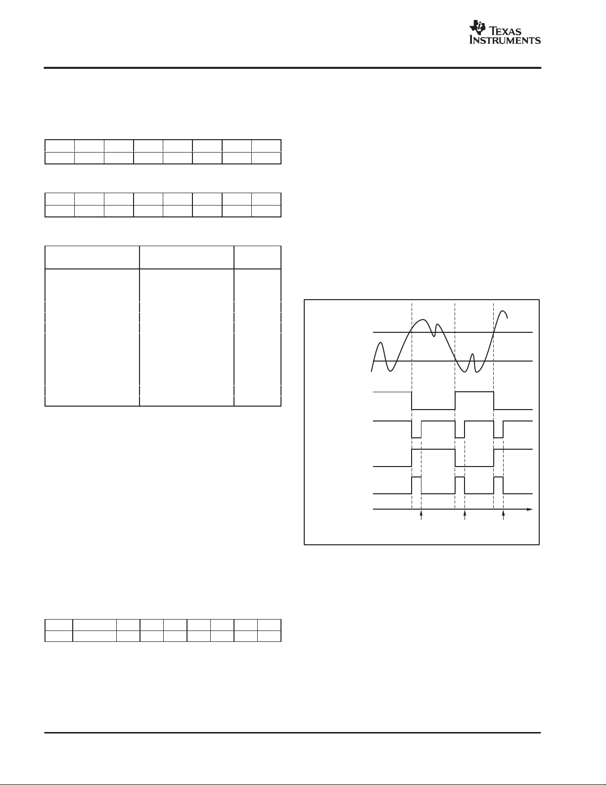
POLARITY (POL)
The Polarity Bit of the TMP101 allows the user to adjust the
polarity of the ALERT pin output. If POL = 0, the ALER T pin
will be active LOW, as shown in Figure 4. For POL = 1 the
ALERT pin will be active HIGH, and the state of the ALERT
pin is inverted.
T
Read
T
HIGH
LOW
Measured
Temperature
TMP101 ALERT PIN
(Comparator Mode)
POL = 0
TMP101 ALERT PIN
(Interrupt Mode)
POL = 0
TMP101 ALERT PIN
(Comparator Mode)
POL = 1
TMP101 ALERT PIN
(Interrupt Mode)
POL = 1
Read Read
Time
Figure 4. Output Transfer Function Diagrams
FAULT QUEUE (F1/F0)
A fault condition occurs when the measured temperature
exceeds the user-defined limits set in the T
Registers. Additionally, the number of fault conditions
required to generate an alert may be programmed using
the Fault Queue. The Fault Queue is provided to prevent
a false alert due to environmental noise. The Fault Queue
requires consecutive fault measurements in order to
trigger the alert function. If the temperature falls below
T
, prior to reaching the number of programmed
LOW
consecutive faults limit, the count is reset to 0. Table 7
defines the number of measured faults that may be
programmed to trigger an alert condition in the device.
HIGH
and T
LOW
6
Page 7

www.ti.com
"#$$
"#$#
SBOS231G − JANUARY 2002 − REVISED NOVEMBER 2007
Table 7. Fault Settings of the TMP100 and
TMP101
F1 F0 CONSECUTIVE FAULTS
0 0 1
0 1 2
1 0 4
1 1 6
CONVERTER RESOLUTION (R1/R0)
The Converter Resolution Bits control the resolution of the
internal Analog-to-Digital (A/D) converter. This allows the
user to maximize efficiency by programming for higher
resolution or faster conversion time. Table 8 identifies the
Resolution Bits and relationship between resolution and
conversion time.
Table 8. Resolution of the TMP100 and TMP101
CONVERSION TIME
R1 R0 RESOLUTION
0 0 9 Bits (0.5°C) 40ms
0 1 10 Bits (0.25°C) 80ms
1 0 11 Bits (0.125°C) 160ms
1 1 12 Bits (0.0625°C) 320ms
(typical)
OS/ALERT (OS)
The TMP100 and TMP101 feature a One-Shot
Temperature Measurement Mode. When the device is in
Shutdown Mode, writing a 1 to the OS/ALERT bit will start
a single temperature conversion. The device will return to
the shutdown state at the completion of the single
conversion. This is useful to reduce power consumption in
the TMP100 and TMP101 when continuous monitoring of
temperature is not required.
Reading the OS/ALERT bit will provide information about
the Comparator Mode status. The state of the POL bit will
invert the polarity of data returned from the OS/ALERT bit.
For POL = 0, the OS/ALERT will read as 1 until the
temperature equals or exceeds T
for the programmed
HIGH
number of consecutive faults, causing the OS/ALERT bit
to read as 0. The OS/ALERT bit will continue to read as 0
until the temperature falls below T
for the programmed
LOW
number of consecutive faults when it will again read as 1.
The status of the TM bit does not affect the status of the
OS/ALERT bit.
HIGH AND LOW LIMIT REGISTERS
In Comparator Mode (TM = 0), the ALERT pin of the
TMP101 becomes active when the temperature equals or
exceeds the value in T
number of faults according to fault bits F1 and F0. The
ALERT pin will remain active until the temperature falls
below the indicated T
faults.
and generates a consecutive
HIGH
value for the same number of
LOW
In Interrupt Mode (TM = 1) the ALERT Pin becomes active
when the temperature equals or exceeds T
HIGH
for a
consecutive number of fault conditions. The ALERT pin
remains active until a read operation of any register occurs
or the device successfully responds to the SMBus Alert
Response Address. The ALERT pin will also be cleared if
the device is placed in Shutdown Mode. Once the ALERT
pin is cleared, it will only become active again by the
temperature falling below T
falls below T
, the ALERT pin will become active and
LOW
. When the temperature
LOW
remain active until cleared by a read operation of any
register or a successful response to the SMBus Alert
Response Address. Once the ALERT pin is cleared, the
above cycle will repeat with the ALERT pin becoming
active when the temperature equals or exceeds T
HIGH
The ALERT pin can also be cleared by resetting the device
with the General Call Reset command. This will also clear
the state of the internal registers in the device returning the
device to Comparator Mode (TM = 0).
Both operational modes are represented in Figure 4.
Table 9 and Table 10 describe the format for the T
registers. Power-up Reset values for T
T
LOW
T
are: T
LOW
the data for T
= 80°C and T
HIGH
HIGH
and T
= 75°C. The format of
LOW
is the same as for the
LOW
HIGH
HIGH
and
and
Temperature Register.
Table 9. Bytes 1 and 2 of T
BYTE D7 D6 D5 D4 D3 D2 D1 D0
1 H11 H10 H9 H8 H7 H6 H5 H4
BYTE D7 D6 D5 D4 D3 D2 D1 D0
2 H3 H2 H1 H0 0 0 0 0
Table 10. Bytes 1 and 2 of T
BYTE D7 D6 D5 D4 D3 D2 D1 D0
1 L11 L10 L9 L8 L7 L6 L5 L4
BYTE D7 D6 D5 D4 D3 D2 D1 D0
2 L3 L2 L1 L0 0 0 0 0
All 12 bits for the Temperature, T
HIGH
HIGH
LOW
, and T
Register
Register
registers
LOW
are used in the comparisons for the ALERT function for all
converter resolutions. The three LSBs in T
HIGH
and T
LOW
can affect the ALERT output even if the converter is
configured for 9-bit resolution.
SERIAL INTERFACE
The TMP100 and TMP101 operate only as slave devices
on the I
made via the open-drain I/O lines SDA and SCL. The
TMP100 and TMP101 support the transmission protocol
for fast (up to 400kHz) and high-speed (up to 3.4MHz)
modes. All data bytes are transmitted most significant bit
first.
2
C bus and SMBus. Connections to the bus are
.
7
Page 8

"#$$
"#$#
SBOS231G − JANUARY 2002 − REVISED NOVEMBER 2007
www.ti.com
SERIAL BUS ADDRESS
To program the TMP100 and TMP101, the master must
first address slave devices via a slave address byte. The
slave address byte consists of seven address bits, and a
direction bit indicating the intent of executing a read or
write operation.
The TMP100 features two address pins to allow up to eight
2
devices to be addressed on a single I
C interface. Table 11
describes the pin logic levels used to properly connect up
to eight devices. Float indicates the pin is left unconnected.
The state of pins ADD0 and ADD1 is sampled on the first
2
I
C bus communication and should be set prior to any
activity on the interface.
Table 11. Address Pins and Slave Addresses for
the TMP100
ADD1 ADD0 SLAVE ADDRESS
0 0 1001000
0 Float 1001001
0 1 1001010
1 0 1001100
1 Float 1001101
1 1 1001110
Float 0 1001011
Float 1 1001111
The TMP101 features one address pin and an ALERT pin,
allowing up to three devices to be connected per bus. Pin
logic levels are described in Table 12. The address pins of
the TMP100 and TMP101 are read after reset or in
response to an I
2
C address acquire request. Following
reading, the state of the address pins is latched to
minimize power dissipation associated with detection.
Table 12. Address Pins and Slave Addresses for
the TMP101
ADD0 SLAVE ADDRESS
0 1001000
Float 1001001
1 1001010
BUS OVERVIEW
The device that initiates the transfer is called a master, and
the devices controlled by the master are slaves. The bus
must be controlled by a master device that generates the
serial clock (SCL), controls the bus access, and generates
the START and STOP conditions.
To address a specific device, a START condition is
initiated, indicated by pulling the data-line (SDA) from a
HIGH to LOW logic level while SCL is HIGH. All slaves on
the bus shift in the slave address byte, with the last bit
indicating whether a read or write operation is intended.
During the ninth clock pulse, the slave being addressed
responds to the master by generating an Acknowledge
and pulling SDA LOW.
Data transfer is then initiated and sent over eight clock
pulses followed by an Acknowledge Bit. During data
transfer SDA must remain stable while SCL is HIGH, as
any change in SDA while SCL is HIGH will be interpreted
as a control signal.
Once all data have been transferred, the master generates
a STOP condition indicated by pulling SDA from LOW to
HIGH, while SCL is HIGH.
WRITING/READING TO THE TMP100 AND
TMP101
Accessing a particular register on the TMP100 and
TMP101 is accomplished by writing the appropriate value
to the Pointer Register. The value for the Pointer Register
is the first byte transferred after the I
with the R/W
bit LOW. Every write operation to the
2
C slave address byte
TMP100 and TMP101 requires a value for the Pointer
Register. (Refer to Figure 6.)
When reading from the TMP100 and TMP101, the last
value stored in the Pointer Register by a write operation is
used to determine which register is read by a read
operation. To change the register pointer for a read
operation, a new value must be written to the Pointer
Register. This is accomplished by issuing an I
address byte with the R/W
bit LOW, followed by the Pointer
2
C slave
Register Byte. No additional data are required. The master
can then generate a START condition and send the I
slave address byte with the R/W
bit HIGH to initiate the
2
read command. See Figure 7 for details of this sequence.
If repeated reads from the same register are desired, it is
not necessary to continually send the Pointer Register
bytes as the TMP100 and TMP101 will remember the
Pointer Register value until it is changed by the next write
operation.
SLAVE MODE OPERATIONS
The TMP100 and TMP101 can operate as slave receivers
or slave transmitters.
Slave Receiver Mode:
The first byte transmitted by the master is the slave
address, with the R/W
then acknowledges reception of a valid address. The next
byte transmitted by the master is the Pointer Register. T h e
TMP100 or TMP101 then acknowledges reception of the
Pointer Register byte. The next byte or bytes are written to
the register addressed by the Pointer Register. The
TMP100 and TMP101 will acknowledge reception of each
data byte. The master may terminate data transfer by
generating a START or STOP condition.
Slave Transmitter Mode:
The first byte is transmitted by the master and is the slave
address, with the R/W
reception of a valid slave address. The next byte is
transmitted by the slave and is the most significant byte of
the register indicated by the Pointer Register. The master
bit LOW. The TMP100 or TMP101
bit HIGH. The slave acknowledges
C
8
Page 9

www.ti.com
"#$$
"#$#
SBOS231G − JANUARY 2002 − REVISED NOVEMBER 2007
acknowledges reception of the data byte. The next byte
transmitted by the slave is the least significant byte. The
master acknowledges reception of the data byte. The
master may terminate data transfer by generating a
Not-Acknowledge on reception of any data byte, or
generating a START or STOP condition.
SMBus ALERT FUNCTION
The TMP101 supports the SMBus Alert function. When
the TMP101 is operating in Interrupt Mode (TM = 1), the
ALERT pin of the TMP101 may be connected as an
SMBus Alert signal. When a master senses that an ALERT
condition is present on the ALERT line, the master sends
an SMBus Alert command (00011001) on the bus. If the
ALERT pin of the TMP101 is active, the TMP101 will
acknowledge the SMBus Alert command and respond by
returning its slave address on the SDA line. The eighth bit
(LSB) of the slave address byte will indicate if the
temperature exceeding T
caused the ALERT condition. For POL = 0, this bit will be
LOW if the temperature is greater than or equal to T
This bit will be HIGH if the temperature is less than T
The polarity of this bit will be inverted if POL = 1. Refer to
Figure 8 for details of this sequence.
If multiple devices on the bus respond to the SMBus Alert
command, arbitration during the slave address portion of
the SMBus alert command will determine which device will
clear its ALERT status. If the TMP101 wins the arbitration,
its ALERT pin will become inactive at the completion of the
SMBus Alert command. If the TMP101 loses the
arbitration, its ALERT pin will remain active.
The TMP100 will also respond to the SMBus ALERT
command if its TM bit is set to 1. Since it does not have an
ALERT pin, the master needs to periodically poll the
device by issuing an SMBus Alert command. If the
TMP100 has generated an ALERT, it will acknowledge the
SMBus Alert command and return its slave address in the
next byte.
or falling below T
HIGH
LOW
HIGH
LOW
GENERAL CALL
The TMP100 and TMP101 respond to the I2C General Call
address (0000000) if the eighth bit is 0. The device will
acknowledge the General Call address and respond to
commands in the second byte. If the second byte is
00000100, the TMP100 and TMP101 will latch the status
of their address pins, but will not reset. If the second byte
is 00000110, the TMP100 and TMP101 will latch the status
of their address pins and reset their internal registers.
POR (POWER-ON RESET)
The TMP100 and TMP101 both have on-chip power-on
reset circuits that reset the device to default settings when
the device is powered on. This circuit activates when the
power supply is less than 0.3V for more than 100ms. If the
TMP100 and TMP101 are powered down by removing
supply voltage from the device, but the supply voltage is
not assured to be less than 0.3V, it is recommended to
issue a General Call reset command on the I
bus to ensure that the TMP100 and TMP101 are
completely reset.
.
.
HIGH-SPEED MODE
In order for the I2C bus to operate at frequencies above
400kHz, the master device must issue an Hs-mode master
code (00001XXX) as the first b yt e af te r a S TART condition
to switch the bus to high-speed operation. The TMP100
and TMP101 will not acknowledge this byte as required by
2
the I
C specification, but will switch their input filters on
SDA and SCL and their output filters on SDA to operate in
Hs-mode, allowing transfers at up to 3.4MHz. After the
Hs-mode master code has been issued, the master will
transmit an I2C slave address to initiate a data transfer
operation. The bus will continue to operate in Hs-mode
until a STOP condition occurs on the bus. Upon receiving
the STOP condition, the TMP100 and TMP101 will switch
their input and output filters back to fast-mode operation.
2
C interface
9
Page 10

"#$$
PARAMETER
UNITS
"#$#
SBOS231G − JANUARY 2002 − REVISED NOVEMBER 2007
www.ti.com
TIMING DIAGRAMS
The TMP100 and TMP101 are I2C and SMBus
compatible. Figure 5 to Figure 8 describe the various
operations on the TMP100 and TMP101. Bus definitions
are given below. Parameters for Figure 5 are defined in
Table 13.
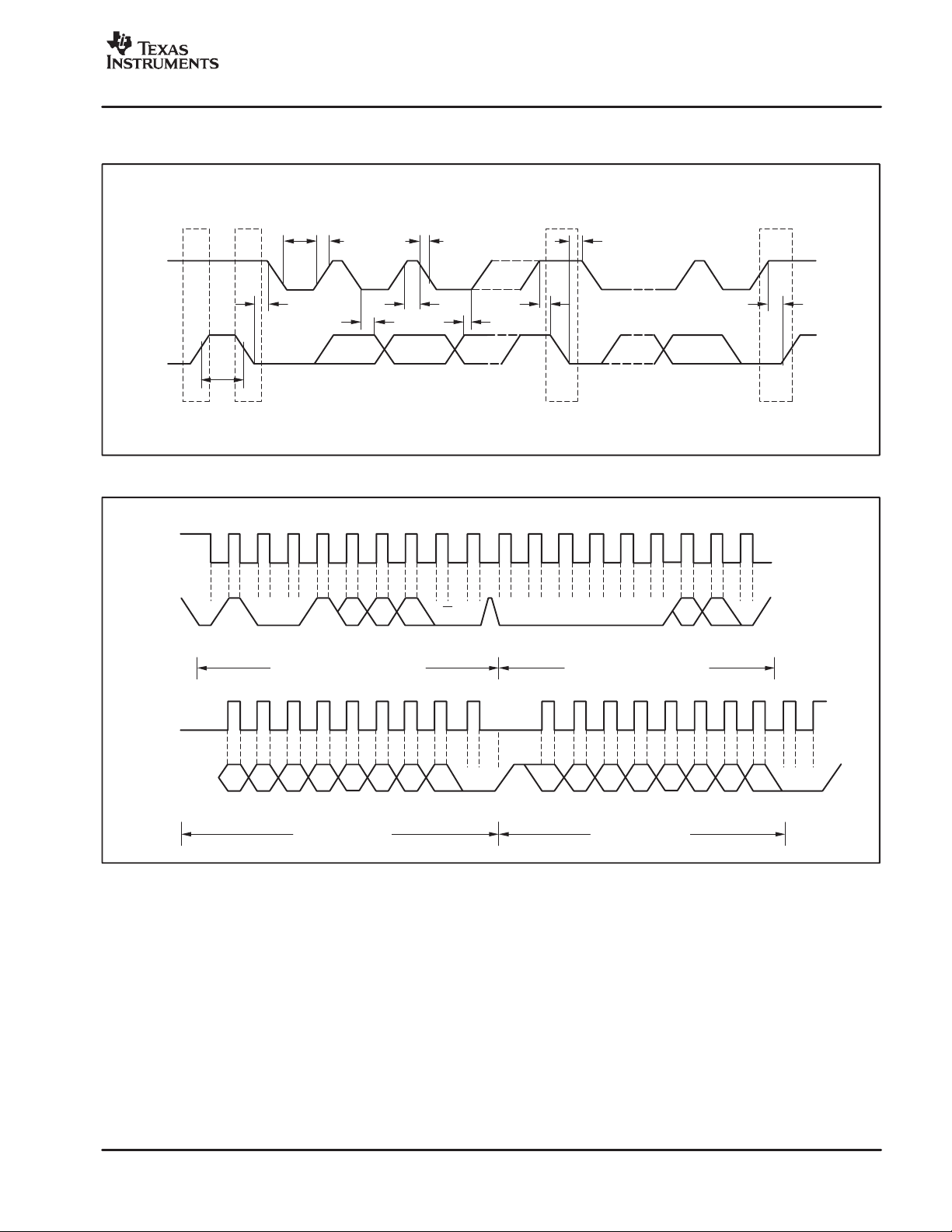
Bus Idle: Both SDA and SCL lines remain HIGH.
Start Data Transfer: A change in the state of the SDA line,
from HIGH to LOW, while the SCL line is HIGH, defines a
START condition. Each data transfer is initiated with a
START condition.
Stop Data Transfer: A change in the state of the SDA line
from LOW to HIGH while the SCL line is HIGH defines a
STOP condition. Each data transfer is terminated with a
repeated START or STOP condition.
Table 13. Timing Diagram Definitions
SCLK Operating Frequency f
Bus Free TIme Between STOP and ST ART Conditions t
Hold time after repeated START condition.
After this period, the first clock is generated.
Repeated START Condition Setup Time t
STOP Condition Setup Time t
Data HOLD Time t
Data Setup Time t
SCLK Clock LOW Period t
SCLK Clock HIGH Period t
Clock/Data Fall Time t
Clock/Data Rise Time t
for SCLK ≤ 100kHz t
(SCLK)
(BUF)
t
(HDSTA)
(SUSTA)
(SUSTO)
(HDDAT)
(SUDAT)
(LOW)
(HIGH)
Data Transfer: The number of data bytes transferred
between a START and a STOP condition is not limited and
is determined by the master device. The receiver
acknowledges the transfer of data.
Acknowledge: Each receiving device, when addressed,
is obliged to generate an Acknowledge bit. A device that
acknowledges must pull down the SDA line during the
Acknowledge clock pulse in such a way that the SDA line
is stable LOW during the HIGH period of the Acknowledge
clock pulse. Setup and hold times must be taken into
account. On a master receive, the termination of the data
transfer can be signaled by the master generating a
Not-Acknowledge on the last byte that has been
transmitted by the slave.
FAST MODE HIGH-SPEED MODE
MIN MAX MIN MAX
0.4 3.4 MHz
600 160 ns
600 160 ns
600 160 ns
600 160 ns
0 0 ns
100 10 ns
1300 160 ns
600 60 ns
F
R
R
300 160 ns
300 160 ns
1000 ns
10
Page 11
www.ti.com
I2C TIMING DIAGRAMS
t
SCL
SDA
(LOW)
t
(HDSTA)
t
(BUF)
PS SP
t
R
SBOS231G − JANUARY 2002 − REVISED NOVEMBER 2007
t
F
t
(HIGH)t(SUSTA)
t
(HDDAT)
t
(SUDAT)
Figure 5. I2C Timing Diagram
t
(HDSTA)
"#$$
"#$#
t
(SUSTO)
SCL
(Continued)
SDA
(Continued)
SCL
SDA
Start By
Master
191
1
0 0 1 A2 A1 A0 R/W 0 0 0 0 0 0 P1 P0
ACK By
TMP100 or TMP101
Frame 1 I2C Slave Address Byte Frame 2 Pointer Register Byte
1
D7
D6 D5 D4 D3 D2 D1 D0
Frame3 Data Byte1
9
ACK By
TMP100 or TMP101
1
D7 D6 D5 D4 D3 D2 D1 D0
Frame4 Data Byte2
ACK By
TMP100 or TMP101
Figure 6. I2C Timing Diagram for Write Word Format
9
…
…
9
ACK By
TMP100 or TMP101
Stop By
Master
11
Page 12
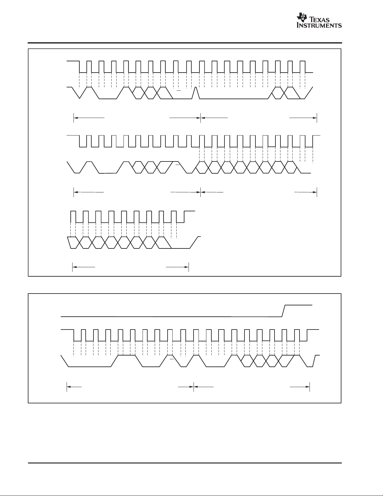
"#$$
"#$#
SBOS231G − JANUARY 2002 − REVISED NOVEMBER 2007
1919
SCL
www.ti.com
…
SDA
SCL
(Continued)
SDA
(Continued)
SCL
(Continued)
SDA
(Continued)
1
001A2A1A0R/W 000000P1P0
Start By
Master
Frame1I2C Slave Address Byte Frame 2 Pointer Register Byte
1919
1 0 0 1 A2 A1 A0 R/W
Start By
Master
Frame3I2C Slave Address Byte Frame 4 Data Byte 1 ReadRegister
19
D7 D6 D5 D4 D3 D2 D1 D0
From
TMP100 or TMP101
Frame5DataByte2ReadRegister
ACK By
TMP100 or TMP101
ACK By
TMP100 or TMP101
ACK By
Master
StopBy
Master
D7 D6 D5 D4 D3 D2 D1 D0
TMP100 or TMP101
TMP100 or TMP101
From
…
ACK By
…
…
ACK By
Master
ALERT
SCL
SDA
StartBy
Master
Figure 7. I2C Timing Diagram for Read Word Format
1919
0001100R/W 1001A2A1A0
ACK By
TMP100 or TMP101
Frame 1 SMBus ALERT ResponseAddress Byte Frame2 SlaveAddress From TMP100
From
TMP100 or TMP101
Status
NACK By
Master
StopBy
Master
Figure 8. Timing Diagram for SMBus ALERT
12
Page 13

PACKAGE OPTION ADDENDUM
www.ti.com
11-Apr-2013
PACKAGING INFORMATION
Orderable Device Status
SN0312100DBVR ACTIVE SOT-23 DBV 6 3000 Green (RoHS
TMP100NA/250 ACTIVE SOT-23 DBV 6 250 Green (RoHS
TMP100NA/250G4 ACTIVE SOT-23 DBV 6 250 Green (RoHS
TMP100NA/3K ACTIVE SOT-23 DBV 6 3000 Green (RoHS
TMP100NA/3KG4 ACTIVE SOT-23 DBV 6 3000 Green (RoHS
TMP101NA/250 ACTIVE SOT-23 DBV 6 250 Green (RoHS
TMP101NA/250G4 ACTIVE SOT-23 DBV 6 250 Green (RoHS
TMP101NA/3K ACTIVE SOT-23 DBV 6 3000 Green (RoHS
TMP101NA/3KG4 ACTIVE SOT-23 DBV 6 3000 Green (RoHS
(1)
The marketing status values are defined as follows:
ACTIVE: Product device recommended for new designs.
LIFEBUY: TI has announced that the device will be discontinued, and a lifetime-buy period is in effect.
NRND: Not recommended for new designs. Device is in production to support existing customers, but TI does not recommend using this part in a new design.
PREVIEW: Device has been announced but is not in production. Samples may or may not be available.
OBSOLETE: TI has discontinued the production of the device.
Package Type Package
(1)
Drawing
Pins Package
Qty
Eco Plan
(2)
& no Sb/Br)
& no Sb/Br)
& no Sb/Br)
& no Sb/Br)
& no Sb/Br)
& no Sb/Br)
& no Sb/Br)
& no Sb/Br)
& no Sb/Br)
Lead/Ball Finish MSL Peak Temp
(3)
CU NIPDAU Level-2-260C-1 YEAR -55 to 125 T100
CU NIPDAU Level-2-260C-1 YEAR T100
CU NIPDAU Level-2-260C-1 YEAR T100
CU NIPDAU Level-2-260C-1 YEAR -55 to 125 T100
CU NIPDAU Level-2-260C-1 YEAR -55 to 125 T100
CU NIPDAU Level-2-260C-1 YEAR -55 to 125 T101
CU NIPDAU Level-2-260C-1 YEAR -55 to 125 T101
CU NIPDAU Level-2-260C-1 YEAR -55 to 125 T101
CU NIPDAU Level-2-260C-1 YEAR -55 to 125 T101
Op Temp (°C) Top-Side Markings
(4)
(2)
Eco Plan - The planned eco-friendly classification: Pb-Free (RoHS), Pb-Free (RoHS Exempt), or Green (RoHS & no Sb/Br) - please check http://www.ti.com/productcontent for the latest availability
information and additional product content details.
TBD: The Pb-Free/Green conversion plan has not been defined.
Pb-Free (RoHS): TI's terms "Lead-Free" or "Pb-Free" mean semiconductor products that are compatible with the current RoHS requirements for all 6 substances, including the requirement that
lead not exceed 0.1% by weight in homogeneous materials. Where designed to be soldered at high temperatures, TI Pb-Free products are suitable for use in specified lead-free processes.
Pb-Free (RoHS Exempt): This component has a RoHS exemption for either 1) lead-based flip-chip solder bumps used between the die and package, or 2) lead-based die adhesive used between
the die and leadframe. The component is otherwise considered Pb-Free (RoHS compatible) as defined above.
Green (RoHS & no Sb/Br): TI defines "Green" to mean Pb-Free (RoHS compatible), and free of Bromine (Br) and Antimony (Sb) based flame retardants (Br or Sb do not exceed 0.1% by weight
in homogeneous material)
Samples
Addendum-Page 1
Page 14

PACKAGE OPTION ADDENDUM
www.ti.com
(3)
MSL, Peak Temp. -- The Moisture Sensitivity Level rating according to the JEDEC industry standard classifications, and peak solder temperature.
11-Apr-2013
(4)
Multiple Top-Side Markings will be inside parentheses. Only one Top-Side Marking contained in parentheses and separated by a "~" will appear on a device. If a line is indented then it is a
continuation of the previous line and the two combined represent the entire Top-Side Marking for that device.
Important Information and Disclaimer:The information provided on this page represents TI's knowledge and belief as of the date that it is provided. TI bases its knowledge and belief on information
provided by third parties, and makes no representation or warranty as to the accuracy of such information. Efforts are underway to better integrate information from third parties. TI has taken and
continues to take reasonable steps to provide representative and accurate information but may not have conducted destructive testing or chemical analysis on incoming materials and chemicals.
TI and TI suppliers consider certain information to be proprietary, and thus CAS numbers and other limited information may not be available for release.
In no event shall TI's liability arising out of such information exceed the total purchase price of the TI part(s) at issue in this document sold by TI to Customer on an annual basis.
OTHER QUALIFIED VERSIONS OF TMP100, TMP101 :
Automotive: TMP101-Q1
•
Enhanced Product: TMP100-EP
•
NOTE: Qualified Version Definitions:
Automotive - Q100 devices qualified for high-reliability automotive applications targeting zero defects
•
Enhanced Product - Supports Defense, Aerospace and Medical Applications
•
Addendum-Page 2
Page 15

PACKAGE MATERIALS INFORMATION
www.ti.com 26-Jan-2013
TAPE AND REEL INFORMATION
*All dimensions are nominal
Device Package
Type
TMP100NA/250 SOT-23 DBV 6 250 178.0 9.0 3.23 3.17 1.37 4.0 8.0 Q3
TMP100NA/3K SOT-23 DBV 6 3000 178.0 9.0 3.23 3.17 1.37 4.0 8.0 Q3
Package
Drawing
Pins SPQ Reel
Diameter
(mm)
Reel
Width
W1 (mm)
A0
(mm)B0(mm)K0(mm)P1(mm)W(mm)
Pin1
Quadrant
Pack Materials-Page 1
Page 16

PACKAGE MATERIALS INFORMATION
www.ti.com 26-Jan-2013
*All dimensions are nominal
Device Package Type Package Drawing Pins SPQ Length (mm) Width (mm) Height (mm)
TMP100NA/250 SOT-23 DBV 6 250 180.0 180.0 18.0
TMP100NA/3K SOT-23 DBV 6 3000 180.0 180.0 18.0
Pack Materials-Page 2
Page 17

Page 18

Page 19

IMPORTANT NOTICE
Texas Instruments Incorporated and its subsidiaries (TI) reserve the right to make corrections, enhancements, improvements and other
changes to its semiconductor products and services per JESD46, latest issue, and to discontinue any product or service per JESD48, latest
issue. Buyers should obtain the latest relevant information before placing orders and should verify that such information is current and
complete. All semiconductor products (also referred to herein as “components”) are sold subject to TI’s terms and conditions of sale
supplied at the time of order acknowledgment.
TI warrants performance of its components to the specifications applicable at the time of sale, in accordance with the warranty in TI’s terms
and conditions of sale of semiconductor products. Testing and other quality control techniques are used to the extent TI deems necessary
to support this warranty. Except where mandated by applicable law, testing of all parameters of each component is not necessarily
performed.
TI assumes no liability for applications assistance or the design of Buyers’ products. Buyers are responsible for their products and
applications using TI components. To minimize the risks associated with Buyers’ products and applications, Buyers should provide
adequate design and operating safeguards.
TI does not warrant or represent that any license, either express or implied, is granted under any patent right, copyright, mask work right, or
other intellectual property right relating to any combination, machine, or process in which TI components or services are used. Information
published by TI regarding third-party products or services does not constitute a license to use such products or services or a warranty or
endorsement thereof. Use of such information may require a license from a third party under the patents or other intellectual property of the
third party, or a license from TI under the patents or other intellectual property of TI.
Reproduction of significant portions of TI information in TI data books or data sheets is permissible only if reproduction is without alteration
and is accompanied by all associated warranties, conditions, limitations, and notices. TI is not responsible or liable for such altered
documentation. Information of third parties may be subject to additional restrictions.
Resale of TI components or services with statements different from or beyond the parameters stated by TI for that component or service
voids all express and any implied warranties for the associated TI component or service and is an unfair and deceptive business practice.
TI is not responsible or liable for any such statements.
Buyer acknowledges and agrees that it is solely responsible for compliance with all legal, regulatory and safety-related requirements
concerning its products, and any use of TI components in its applications, notwithstanding any applications-related information or support
that may be provided by TI. Buyer represents and agrees that it has all the necessary expertise to create and implement safeguards which
anticipate dangerous consequences of failures, monitor failures and their consequences, lessen the likelihood of failures that might cause
harm and take appropriate remedial actions. Buyer will fully indemnify TI and its representatives against any damages arising out of the use
of any TI components in safety-critical applications.
In some cases, TI components may be promoted specifically to facilitate safety-related applications. With such components, TI’s goal is to
help enable customers to design and create their own end-product solutions that meet applicable functional safety standards and
requirements. Nonetheless, such components are subject to these terms.
No TI components are authorized for use in FDA Class III (or similar life-critical medical equipment) unless authorized officers of the parties
have executed a special agreement specifically governing such use.
Only those TI components which TI has specifically designated as military grade or “enhanced plastic” are designed and intended for use in
military/aerospace applications or environments. Buyer acknowledges and agrees that any military or aerospace use of TI components
which have not been so designated is solely at the Buyer's risk, and that Buyer is solely responsible for compliance with all legal and
regulatory requirements in connection with such use.
TI has specifically designated certain components as meeting ISO/TS16949 requirements, mainly for automotive use. In any case of use of
non-designated products, TI will not be responsible for any failure to meet ISO/TS16949.
Products Applications
Audio www.ti.com/audio Automotive and Transportation www.ti.com/automotive
Amplifiers amplifier.ti.com Communications and Telecom www.ti.com/communications
Data Converters dataconverter.ti.com Computers and Peripherals www.ti.com/computers
DLP® Products www.dlp.com Consumer Electronics www.ti.com/consumer-apps
DSP dsp.ti.com Energy and Lighting www.ti.com/energy
Clocks and Timers www.ti.com/clocks Industrial www.ti.com/industrial
Interface interface.ti.com Medical www.ti.com/medical
Logic logic.ti.com Security www.ti.com/security
Power Mgmt power.ti.com Space, Avionics and Defense www.ti.com/space-avionics-defense
Microcontrollers microcontroller.ti.com Video and Imaging www.ti.com/video
RFID www.ti-rfid.com
OMAP Applications Processors www.ti.com/omap TI E2E Community e2e.ti.com
Wireless Connectivity www.ti.com/wirelessconnectivity
Mailing Address: Texas Instruments, Post Office Box 655303, Dallas, Texas 75265
Copyright © 2013, Texas Instruments Incorporated
Page 20

 Loading...