

查询TM2SN64EPH供应商
D
Organization:
– TM2SN64EPH . . . 2 097 152 x 64 Bits
– TM4SN64EPH . . . 4 194 304 x 64 Bits
D
Single 3.3-V Power Supply
(±10% Tolerance)
D
Designed for 66-MHz 4-Clock Systems
D
JEDEC 168-Pin Dual-In-Line Memory
Module (DIMM) Without Buffer for Use With
Socket
D
TM2SN64EPH — Uses Eight 16M-Bit
Synchronous Dynamic RAMs (SDRAMs)
(2M × 8-Bit) in Plastic Thin Small-Outline
Packages (TSOPs)
D
TM4SN64EPH — Uses Sixteen 16M-Bit
SDRAMs (2M × 8-Bit) in Plastic TSOPs
D
Byte-Read/Write Capability
D
Performance Ranges:
SYNCHRONOUS
CLOCK CYCLE
TIME
t
CK3
†
(CL = 3)
’xSN64EPH-10 10 ns 15 ns 7.5 ns 7.5 ns 64 ms
†
CL = CAS latency
t
CK2
(CL = 2)
ACCESS TIME
CLOCK TO
OUTPUT
t
AC3
(CL = 3)
t
AC2
(CL = 2)
REFRESH
INTERV AL
TM2SN64EPH 2097152 BY 64-BIT
TM4SN64EPH 4194304 BY 64-BIT
SYNCHRONOUS DYNAMIC RAM MODULES
SMMS706A – MARCH 1998 – REVISED APRIL 1998
D
High-Speed, Low-Noise, Low-Voltage TTL
(LVTTL) Interface
D
Read Latencies 2 and 3 Supported
D
Support Burst-Interleave and
Burst-Interrupt Operations
D
Burst Length Programmable to 1, 2, 4,
and 8
D
Two Banks for On-Chip Interleaving
(Gapless Access)
D
Ambient Temperature Range
0°C to 70°C
D
Gold-Plated Contacts
D
Pipeline Architecture
D
Serial Presence Detect (SPD) Using
EEPROM
description
The TM2SN64EPH is a 16M-byte, 168-pin dual-in-line memory module (DIMM). The DIMM is composed of
eight TMS626812BDGE, 2097152 x 8-bit SDRAMs, each in a 400-mil, 44-pin plastic thin small-outline package
(TSOP) mounted on a substrate with decoupling capacitors. See the TMS626812B data sheet (literature
number SMOS693).
The TM4SN64EPH is a 32M-byte, 168-pin DIMM. The DIMM is composed of sixteen TMS626812BDGE,
2 097152 x 8-bit SDRAMs, each in a 400-mil, 44-pin plastic TSOP mounted on a substrate with decoupling
capacitors.
operation
The TM2SN64EPH operates as eight TMS626812BDGE devices that are connected as shown in the
TM2SN64EPH functional block diagram. The TM4SN64EPH operates as sixteen TMS626812BDGE devices
connected as shown in the TM4SN64EPH functional block diagram.
Please be aware that an important notice concerning availability, standard warranty, and use in critical applications of
Texas Instruments semiconductor products and disclaimers thereto appears at the end of this data sheet.
PRODUCTION DATA information is current as of publication date.
Products conform to specifications per the terms of Texas Instruments
standard warranty. Production processing does not necessarily include
testing of all parameters.
POST OFFICE BOX 1443 • HOUSTON, TEXAS 77251–1443
Copyright 1998, Texas Instruments Incorporated
1
TM2SN64EPH 2097152 BY 64-BIT
TM4SN64EPH 4194304 BY 64-BIT
SYNCHRONOUS DYNAMIC RAM MODULES
SMMS706A – MARCH 1998 – REVISED APRIL 1998
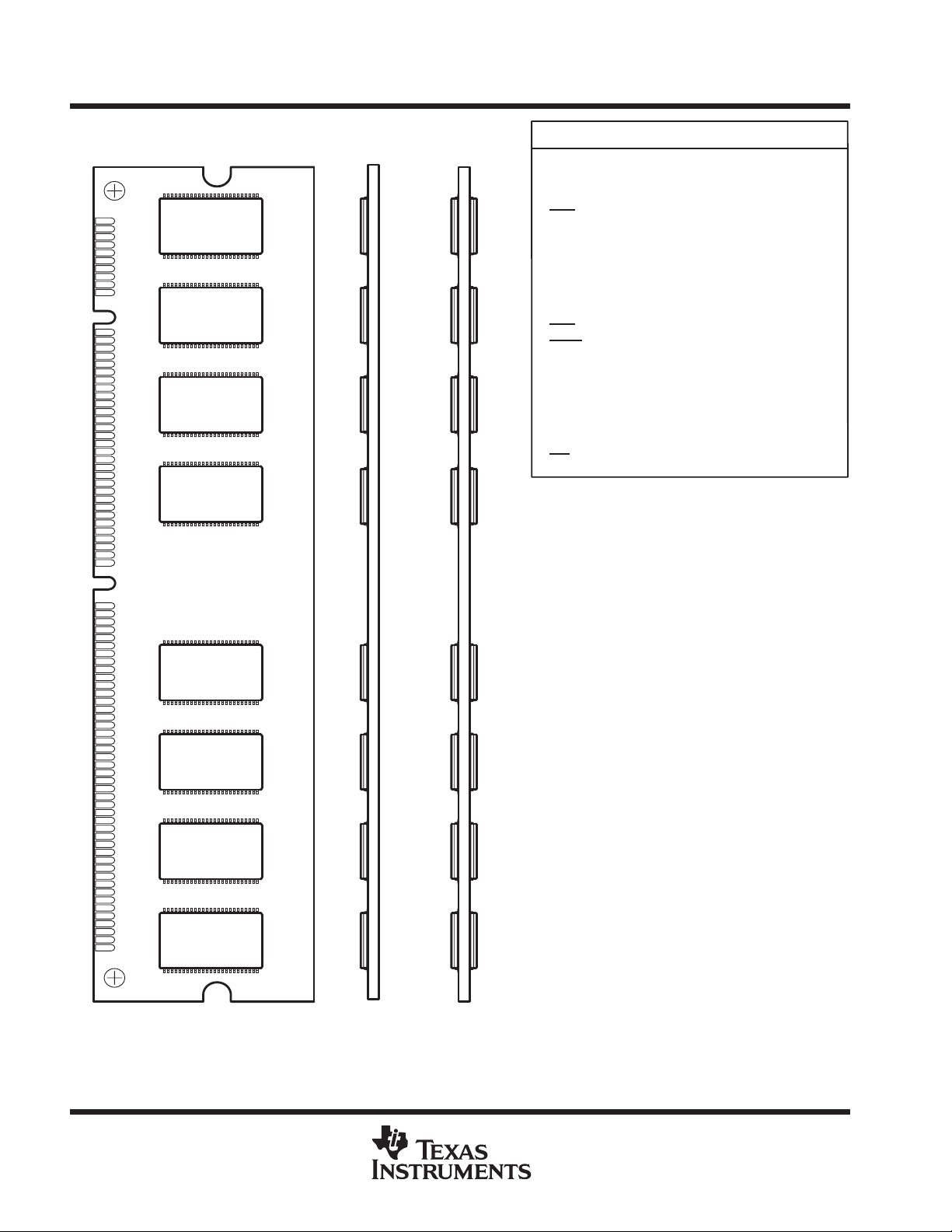
DUAL-IN-LINE MEMORY MODULE
(TOP VIEW)
1
10
11
40
TM2SN64EPH
(SIDE VIEW)
TM4SN64EPH
(SIDE VIEW)
PIN NOMENCLATURE
A[0:10] Row-Address Inputs
A[0:8] Column-Address Inputs
A11/BA0 Bank-Select Zero
CAS
CKE[0:1] Clock Enable
CK[0:3] System Clock
DQ[0:63] Data-In/Data-Out
DQMB[0:7] Data-In/Data-Out
NC No Connect
RAS Row-Address Strobe
S[0:3] Chip-Select
SA[0:2] Serial Presence Detect (SPD)
SCL SPD Clock
SDA SPD Address/Data
V
DD
V
SS
WE
Column-Address Strobe
Mask Enable
Device Address Input
3.3-V Supply
Ground
Write Enable
41
84
2
POST OFFICE BOX 1443 • HOUSTON, TEXAS 77251–1443
TM2SN64EPH 2097152 BY 64-BIT
TM4SN64EPH 4194304 BY 64-BIT
SYNCHRONOUS DYNAMIC RAM MODULES
SMMS706A – MARCH 1998 – REVISED APRIL 1998
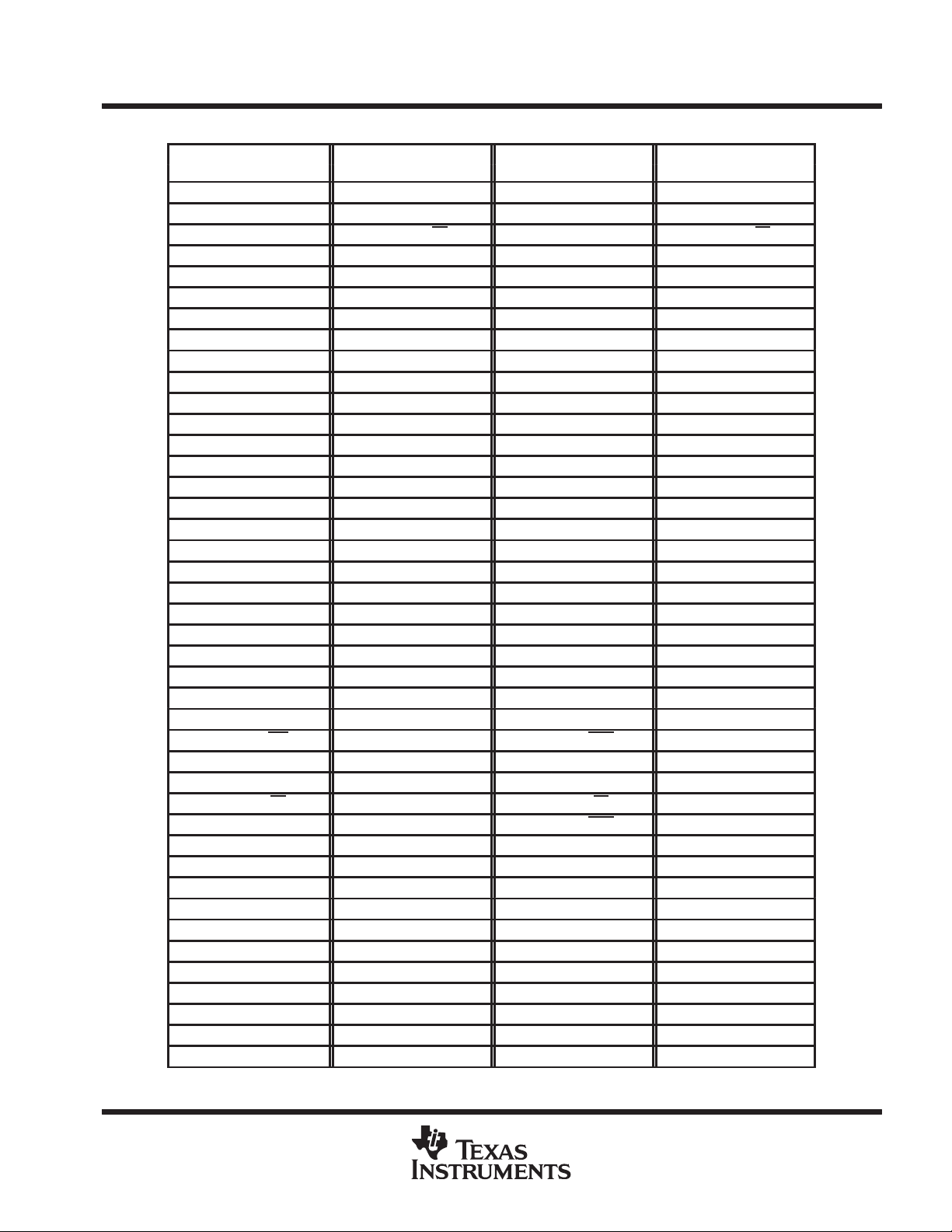
Pin Assignments
PIN PIN PIN PIN
NO. NAME NO. NAME NO. NAME NO. NAME
1 V
2 DQ0 44 NC 86 DQ32 128 CKE0
3 DQ1 45 S2 87 DQ33 129 S3
4 DQ2 46 DQMB2 88 DQ34 130 DQMB6
5 DQ3 47 DQMB3 89 DQ35 131 DQMB7
6 V
7 DQ4 49 V
8 DQ5 50 NC 92 DQ37 134 NC
9 DQ6 51 NC 93 DQ38 135 NC
10 DQ7 52 NC 94 DQ39 136 NC
11 DQ8 53 NC 95 DQ40 137 NC
12 V
13 DQ9 55 DQ16 97 DQ41 139 DQ48
14 DQ10 56 DQ17 98 DQ42 140 DQ49
15 DQ11 57 DQ18 99 DQ43 141 DQ50
16 DQ12 58 DQ19 100 DQ44 142 DQ51
17 DQ13 59 V
18 V
19 DQ14 61 NC 103 DQ46 145 NC
20 DQ15 62 NC 104 DQ47 146 NC
21 NC 63 CKE1 105 NC 147 NC
22 NC 64 V
23 V
24 NC 66 DQ22 108 NC 150 DQ54
25 NC 67 DQ23 109 NC 151 DQ55
26 V
27 WE 69 DQ24 111 CAS 153 DQ56
28 DQMB0 70 DQ25 112 DQMB4 154 DQ57
29 DQMB1 71 DQ26 113 DQMB5 155 DQ58
30 S0 72 DQ27 114 S1 156 DQ59
31 NC 73 V
32 V
33 A0 75 DQ29 117 A1 159 DQ61
34 A2 76 DQ30 118 A3 160 DQ62
35 A4 77 DQ31 119 A5 161 DQ63
36 A6 78 V
37 A8 79 CK2 121 A9 163 CK3
38 A10 80 NC 122 A11/BA0 164 NC
39 NC 81 NC 123 NC 165 SA0
40 V
41 V
42 CK0 84 V
SS
DD
SS
DD
SS
DD
SS
DD
DD
43 V
48 NC 90 V
54 V
60 DQ20 102 V
65 DQ21 107 V
68 V
74 DQ28 116 V
82 SDA 124 V
83 SCL 125 CK1 167 SA2
SS
DD
SS
DD
SS
SS
DD
SS
DD
85 V
91 DQ36 133 V
96 V
101 DQ45 143 V
106 NC 148 V
110 V
115 RAS 157 V
120 A7 162 V
126 NC 168 V
SS
DD
SS
DD
SS
DD
SS
DD
127 V
132 NC
138 V
144 DQ52
149 DQ53
152 V
158 DQ60
166 SA1
SS
DD
SS
DD
SS
SS
DD
SS
DD
POST OFFICE BOX 1443 • HOUSTON, TEXAS 77251–1443
3
TM2SN64EPH 2097152 BY 64-BIT
TM4SN64EPH 4194304 BY 64-BIT
SYNCHRONOUS DYNAMIC RAM MODULES
SMMS706A – MARCH 1998 – REVISED APRIL 1998
dual-in-line memory module and components
The dual-in-line memory module and components include:
D
PC substrate: 1,27 ± 0,1 mm (0.05 inch) nominal thickness; 0.005 inch/inch maximum warpage
D
Bypass capacitors: Multilayer ceramic
D
Contact area: Nickel plate and gold plate over copper
functional block diagram for the TM2SN64EPH
DQMB0
DQ[0:7]
DQMB1
DQ[8:15]
DQMB2
DQ[16:23]
S0
S2
8
8
8
CS
DQM
DQ[0:7]
CS
DQM
DQ[0:7]
CS
DQM
DQ[0:7]
U0
U1
U2
DQMB4
DQ[32:39]
DQMB5
DQ[40:47]
DQMB6
DQ[48:55]
R
C
CS
U4
8
8
8
DQM
DQ[0:7]
CS
U5
DQM
DQ[0:7]
CS
U6
DQM
DQ[0:7]
RR
RR
RR
CK0
CK1
CK2
CK3
R = 10 Ω
RC = 10 Ω
C = 10 pF
V
DD
V
SS
R
C
R
C
R
C
R
C
R
C
Two 0.1 µF
(minimum) per
SDRAM
CK: U0, U4
CK: U1, U5
CK: U2, U6
CK: U3, U7
C
C
U[0:7]
U[0:7]
CS
U3
DQMB3
DQ[24:31]
RAS RAS: SDRAM U[0:7]
CAS CAS: SDRAM U[0:7]
WE
CKE0
A[0:11]
4
8
DQM
DQ[0:7]
WE: SDRAM U[0:7]
CKE: SDRAM U[0:7]
A[0:11]: SDRAM U[0:7]
CS
DQMB7
DQ[56:63]
POST OFFICE BOX 1443 • HOUSTON, TEXAS 77251–1443
RR
DQM
8
DQ[0:7]
LEGEND: CS
SPD = Serial Presence Detect
U7
= Chip Select
SPD EEPROM
SCL SDA
A0 A1 A2
SA0 SA1 SA2
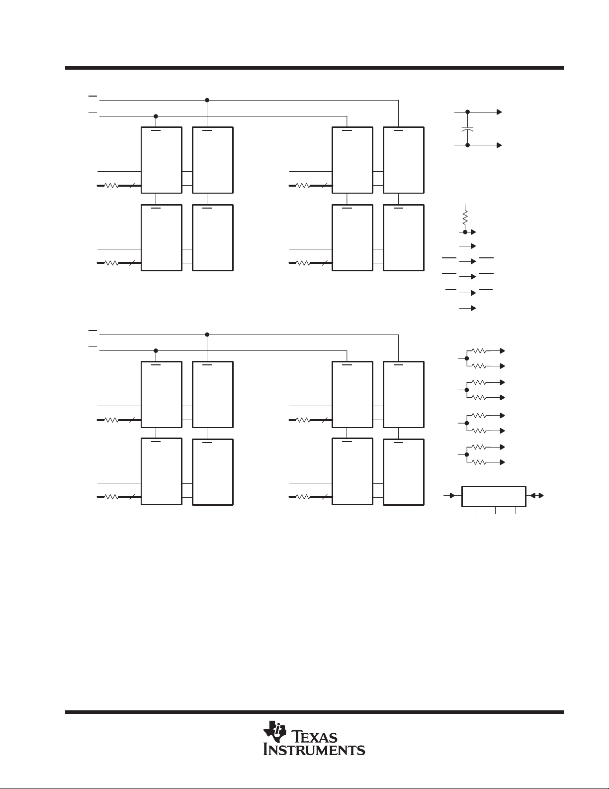
functional block diagram for the TM4SN64EPH
S1
S0
CS
U0
DQMB0 DQMB4
DQ[0:7] DQ[0:7]
DQMB1
DQ[8:15]
R
R
DQM DQM
8
CS
U1
DQM
8
DQ[0:7]
CS
UB0
DQM
DQ[0:7]
CS
UB1
DQM
DQ[0:7]
DQ[32:39]
DQMB5
DQ[40:47]
TM2SN64EPH 2097152 BY 64-BIT
TM4SN64EPH 4194304 BY 64-BIT
SYNCHRONOUS DYNAMIC RAM MODULES
SMMS706A – MARCH 1998 – REVISED APRIL 1998
V
DD
CS
U4
R
8
DQ[0:7]
CS
U5
8
DQM
DQ[0:7]
R
CS
UB4
DQM
DQ[0:7]
CS
UB5
DQM
DQ[0:7]
V
SS
CKE1 CKE: UB[0:7]
CKE0
RAS RAS: U[0:7], UB[0:7]
CAS CAS: U[0:7], UB[0:7]
WE
A[0:11]
Two 0.1 µF
(minimum) per
SDRAM
V
DD
10 kΩ
CKE: U[0:7]
WE: U[0:7], UB[0:7]
A[0:11]: U[0:7], UB[0:7]
U[0:7], UB[0:7]
U[0:7], UB[0:7]
DQMB2
DQ[16:23]
DQMB3
DQ[24:31]
S3
S2
8
8
CS
U2
DQM
DQ[0:7]
CS
U3
DQM
DQ[0:7]
CS
UB2
DQM
DQ[0:7]
CS
UB3
DQM
DQ[0:7]
DQMB6
DQ[48:55]
DQMB7
DQ[56:63]
R = 10 Ω
RC = 10 Ω
R
C
C
C
C
C
C
C
C
CK: U0, U4
CK: U1, U5
CK: UB0, UB4
CK: UB1, UB5
CK: U2, U6
CK: U3, U7
CK: UB2, UB6
CK: UB3, UB7
CK0
CS
U6
8
8
DQM
DQ[0:7]
CS
U7
DQM
DQ[0:7]
RR
RR
CS
UB6
DQM
DQ[0:7]
CS
UB7
DQM
DQ[0:7]
CK1
CK2
CK3
R
R
R
R
R
R
R
SPD EEPROM
SCL SDA
A0 A1 A2
SA0 SA1 SA2
POST OFFICE BOX 1443 • HOUSTON, TEXAS 77251–1443
5

TM2SN64EPH 2097152 BY 64-BIT
PARAMETER
UNIT
TM4SN64EPH 4194304 BY 64-BIT
SYNCHRONOUS DYNAMIC RAM MODULES
SMMS706A – MARCH 1998 – REVISED APRIL 1998
absolute maximum ratings over operating ambient temperature range (unless otherwise noted)
Supply voltage range, V
Voltage range on any pin (see Note 1) – 0.5 V to 4.6 V. . . . . . . . . . . . . . . . . . . . . . . . . . . . . . . . . . . . . . . . . . . . . .
Short-circuit output current 50 mA. . . . . . . . . . . . . . . . . . . . . . . . . . . . . . . . . . . . . . . . . . . . . . . . . . . . . . . . . . . . . . . .
Power dissipation: TM2SN64EPH 8 W. . . . . . . . . . . . . . . . . . . . . . . . . . . . . . . . . . . . . . . . . . . . . . . . . . . . . . . . . . . .
TM4SN64EPH 16 W. . . . . . . . . . . . . . . . . . . . . . . . . . . . . . . . . . . . . . . . . . . . . . . . . . . . . . . . . . .
Operating ambient temperature range, T
Storage temperature range, T
†
Stresses beyond those listed under “absolute maximum ratings” may cause permanent damage to the device. These are stress ratings only, and
functional operation of the device at these or any other conditions beyond those indicated under “recommended operating conditions” is not
implied. Exposure to absolute-maximum-rated conditions for extended periods may affect device reliability.
NOTE 1: All voltage values are with respect to VSS.
–0.5 V to 4.6 V. . . . . . . . . . . . . . . . . . . . . . . . . . . . . . . . . . . . . . . . . . . . . . . . . . . . . . . . .
DD
0°C to 70°C. . . . . . . . . . . . . . . . . . . . . . . . . . . . . . . . . . . . . . . . . . . . . .
– 55°C to 150°C. . . . . . . . . . . . . . . . . . . . . . . . . . . . . . . . . . . . . . . . . . . . . . . . . .
stg
A
recommended operating conditions
MIN NOM MAX UNIT
V
DD
V
SS
V
IH
V
IH-SPD
V
IL
T
A
‡
VIL MIN = –1.5 V ac (pulse width v 5 ns)
Supply voltage 3 3.3 3.6 V
Supply voltage 0 V
High-level input voltage 2 VDD + 0.3 V
High-level input voltage for the SPD device 2 5.5 V
Low-level input voltage
Operating ambient temperature 0 70 °C
‡
–0.3 0.8 V
capacitance over recommended ranges of supply voltage and ambient temperature,
f = 1 MHz (see Note 2)
C
i(CK)
C
i(AC)
C
i(CKE)
C
o
C
i(DQMBx)
C
i(Sx)
C
i/o(SDA)
C
i(SPD)
§
Specifications in this table represent a single SDRAM device.
NOTE 2: VDD = 3.3 V ± 0.3 V. Bias on pins under test is 0 V.
Input capacitance, CK input 2.5 4 pF
Input capacitance, address and control inputs: A0–A11, RAS, CAS, WE 2.5 5 pF
Input capacitance, CKE input 5 pF
Output capacitance 4 6.5 pF
Input capacitance, DQMBx input 2.5 5 pF
Input capacitance, Sx input 2.5 5 pF
Input/output capacitor , SDA input 9 pF
Input capacitor, SA0, SA1, SA2, SCL inputs 7 pF
§
TMxSN64EPH
MIN MAX
†
6
POST OFFICE BOX 1443 • HOUSTON, TEXAS 77251–1443

PARAMETER
TEST CONDITIONS
UNIT
I
Operating current
IOH/I
d
mA
gy
mA
gy
mA
y
mA
y
mA
I
Burst current
All bank
mA
I
Auto-refresh current
t
≤ t
MIN
mA
TM2SN64EPH 2097152 BY 64-BIT
TM4SN64EPH 4194304 BY 64-BIT
SYNCHRONOUS DYNAMIC RAM MODULES
SMMS706A – MARCH 1998 – REVISED APRIL 1998
electrical characteristics over recommended ranges of supply voltage and ambient temperature
(unless otherwise noted) (see Note 3)
V
OH
V
OL
I
I
I
O
CC1
I
CC2P
I
CC2PS
I
CC2N
I
CC2NS
I
CC3P
I
CC3PS
I
CC3N
I
CC3NS
CC4
CC5
I
CC6
†
Specifications in this table represent a single SDRAM device.
NOTES: 3. All specifications apply to the device after power-up initialization. All control and address inputs must be stable and valid.
High-level output voltage IOH = – 2 mA 2.4 V
Low-level output voltage IOL = 2 mA 0.4 V
Input current (leakage) 0 V < VI < VDD + 0.3 V, All other pins = 0 V to V
Output current (leakage) 0 V < VO < VDD Output disabled
p
Precharge standby current in
power-down mode
Precharge standby current in
non-power-down mode
Active standby current in
power-down mode
Active standby current in
non-power-down mode
Self-refresh current CKE ≤ VIL MAX 0.4 mA
4. Control, DQ, and address inputs change state twice during tRC.
5. Control, DQ, and address inputs change state once every 30 ns.
6. Control, DQ, and address inputs do not change.
7. Control, DQ, and address inputs change once every cycle.
†
’xSN64EPH- 10
MIN MAX
"
DD
Burst length = 1, tRC ≥ tRC MIN
= 0 mA, one bank activate
OL
(see Note 4)
CKE ≤ VIL MAX, tCK = 15 ns (see Note 5) 1
CKE and CK ≤ VIL MAX, tCK = ∞ (see Note 6) 1
CKE ≥ VIH MIN, tCK = 15 ns (see Note 5) 30
CKE ≥ VIH MIN, CK ≤ VIL MAX, tCK = ∞ (see Note 6) 2
CKE ≤ VIL MAX, tCK = 15 ns (see Note 5) 3
CKE and CK ≤ VIL MAX, tCK = ∞ (see Note 6) 3
CKE ≥ VIH MIN, tCK = 15 ns (see Note 5) 40
CKE ≥ VIH MIN, CK ≤ VIL MAX, tCK = ∞ (see Note 6) 10
Page burst, IOH/IOL = 0 mA
s activated, n
(see Note 7)
RC
RC
= one cycle
CCD
CAS latency = 2
CAS latency = 3
CAS latency = 2 130
CAS latency = 3 140
CAS latency = 2 80
CAS latency = 3 85
10 µA
"
10 µA
85
90
POST OFFICE BOX 1443 • HOUSTON, TEXAS 77251–1443
7

TM2SN64EPH 2097152 BY 64-BIT
UNIT
TM4SN64EPH 4194304 BY 64-BIT
SYNCHRONOUS DYNAMIC RAM MODULES
SMMS706A – MARCH 1998 – REVISED APRIL 1998
ac timing requirements
t
CK2
t
CK3
t
CH
t
CL
t
AC2
t
AC3
t
OH
t
LZ
t
HZ
t
IS
t
IH
t
CESP
t
RAS
t
RC
t
RCD
t
RP
t
RRD
t
RSA
t
APR
t
APW
t
T
t
REF
n
n
n
n
n
n
n
n
n
n
†
All references are made to the rising transition of CK unless otherwise noted.
NOTES: 8. tAC is referenced from the rising transition of CK that precedes the data-out cycle. For example, the first data out tAC is referenced
Cycle time, CLK, CAS latency = 2 15 ns
Cycle time, CLK, CAS latency = 3 10 ns
Pulse duration, CLK high 3 ns
Pulse duration, CLK low 3 ns
Access time, CLK high to data out, CAS latency = 2 (see Note 8) 7.5 ns
Access time, CLK high to data out, CAS latency = 3 (see Note 8) 7.5 ns
Hold time, CLK high to data out 3 ns
Delay time, CLK high to DQ in low-impedance state (see Note 9) 2 ns
Delay time, CLK high to DQ in high-impedance state (see Note 10) 8 ns
Setup time, address, control, and data input 2 ns
Hold time, address, control, and data input 1 ns
Power-down/self-refresh exit time 10 ns
Delay time, ACTV command to DEAC or DCAB command 50 100000 ns
Delay time, ACTV, REFR, or SLFR exit to ACTV, MRS, REFR, or SLFR command 80 ns
Delay time, ACTV command to READ, READ-P, WRT, or WRT-P command (see Note 11) 20 ns
Delay time, DEAC or DCAB command to ACTV, MRS, REFR, or SLFR command 30 ns
Delay time, ACTV command in one bank to ACTV command in the other bank 30 ns
Delay time, MRS command to ACTV , MRS, REFR, or SLFR command 20 ns
Final data out of READ-P operation to ACTV , MRS, SLFR, or REFR command tRP – (CL –1) * t
Final data in of WRT-P operation to ACTV, MRS, SLFR, or REFR command tRP + t
Transition time (see Note 12) 1 5 ns
Refresh interval 64 ms
Delay time, READ or WRT command to an interrupting command 1 cycle
CCD
Delay time, CS low or high to input enabled or inhibited 0 0 cycle
CDD
Delay time, CKE high or low to CLK enabled or disabled 1 1 cycle
CLE
Delay time, final data in of WRT operation to READ, READ-P, WRT, WRT-P 1 cycle
CWL
Delay time, ENBL or MASK command to enabled or masked data in 0 0 cycle
DID
Delay time, ENBL or MASK command to enabled or masked data out 2 2 cycle
DOD
Delay time, DEAC or DCAB command to DQ in high-impedance state, CAS latency = 2 2 cycle
HZP2
Delay time, DEAC or DCAB command to DQ in high-impedance state, CAS latency = 3 3 cycle
HZP3
Delay time, WRT command to first data in 0 0 cycle
WCD
Delay time, final data in of WRT operation to DEAC or DCAB command 1 cycle
WR
from the rising transition of CK that is CAS latency – one cycle after the READ command. Access time is measured at output
reference level 1.4 V.
9. tLZ is measured from the rising transition of CK that is CAS latency – one cycle after the READ command.
10. tHZ MAX defines the time at which the outputs are no longer driven and is not referenced to output voltage levels.
11. For read or write operations with automatic deactivate, t
12. Transition time, tT, is measured between VIH and VIL.
†
’xSN64EPH-10
MIN MAX
ns
ns
must be set to satisfy minimum t
RCD
RAS
CK
CK
.
8
POST OFFICE BOX 1443 • HOUSTON, TEXAS 77251–1443

DESCRIPTION OF FUNCTION
TM2SN64EPH 2097152 BY 64-BIT
TM4SN64EPH 4194304 BY 64-BIT
SYNCHRONOUS DYNAMIC RAM MODULES
SMMS706A – MARCH 1998 – REVISED APRIL 1998
serial presence detect
The serial presence detect (SPD) is contained in a 256-byte serial EEPROM located on the module. The SPD
nonvolatile EEPROM contains various data such as module configuration, SDRAM organization, and timing
parameters (see Table 1 and Table 2). Only the first 128 bytes are programmed by Texas Instruments; the
remaining 128 bytes are available for customer use. Programming is done through an IIC bus using the clock
(SCL) and data (SDA) signals. All Texas Instruments modules comply with the current JEDEC SPD Standard.
See the Texas
further details.
SPD contents for the TMxSN64EPH devices are listed in the following tables:.
Instruments
Serial Presence Detect Technical Reference
Table 1 – TM2SN64EPH Table 2 – TM4SN64EPH
Table 1. Serial Presence Detect Data for the TM2SN64EPH
(literature number SMMU001) for
BYTE
NO.
0 Defines number of bytes written into serial memory during module manufacturing 128 bytes 80h
1 Total number of bytes of SPD memory device 256 bytes 08h
2 Fundamental memory type (FPM, EDO, SDRAM, . . .) SDRAM 04h
3 Number of row addresses on this assembly 11 0Bh
4 Number of column addresses on this assembly 9 09h
5 Number of module rows on this assembly 1 bank 01h
6 Data width of this assembly 64 bits 40h
7 Data width continuation 00h
8 Voltage interface standard of this assembly LVTTL 01h
9 SDRAM cycle time at maximum supported CAS latency (CL), CL = X tCK = 10 ns A0h
10 SDRAM access from clock at CL = X tAC = 7.5 ns 75h
11 DIMM configuration type (non-parity, parity, error correcting code [ECC]) Non-Parity 00h
12 Refresh rate/type
13 SDRAM width, primary DRAM x8 08h
14 Error-checking SDRAM data width N/A 00h
15 Minimum clock delay, back-to-back random column addresses 1 CK cycle 01h
16 Burst lengths supported 1, 2, 4, 8 0Fh
17 Number of banks on each SDRAM device 2 banks 02h
18 CAS latencies supported 2, 3 06h
19 CS latency 0 01h
20 Write latency 0 01h
21 SDRAM module attributes
22 SDRAM device attributes: general
23 Minimum clock cycle time at CL = X – 1 tCK = 15 ns F0h
24 Maximum data-access time from clock at CL = X – 1 tAC = 7.5 ns 75h
25 Minimum clock cycle time at CL = X – 2 N/A 00h
TM2SN64EPH-10
ITEM DATA
15.6 µs/
self-refresh
Non-buffered/
Non-registered
VDD tolerance =
(+10%),
Burst read/write,
precharge all,
auto precharge
80h
00h
0Eh
POST OFFICE BOX 1443 • HOUSTON, TEXAS 77251–1443
9

TM2SN64EPH 2097152 BY 64-BIT
DESCRIPTION OF FUNCTION
TM4SN64EPH 4194304 BY 64-BIT
SYNCHRONOUS DYNAMIC RAM MODULES
SMMS706A – MARCH 1998 – REVISED APRIL 1998
serial presence detect (continued)
Table 1. Serial Presence Detect Data for the TM2SN64EPH (Continued)
BYTE
NO.
26 Maximum data-access time from clock at CL = X – 2 N/A 00h
27 Minimum row-precharge time tRP = 20 ns 14h
28 Minimum row-active to row-active delay t
29 Minimum RAS-to-CAS delay t
30 Minimum RAS pulse width t
31 Density of each bank on module 16M Bytes 04h
32 Command and address signal input setup time tIS = 2 ns 20h
33 Command and address signal input hold time tIH = 1 ns 10h
34 Data signal input setup time tIS = 2 ns 20h
35 Data signal input hold time tIH = 1 ns 10h
36–61 Superset features (may be used in the future)
62 SPD revision Rev. 1.2 12h
63 Checksum for byte 0–62 250 FAh
64–71 Manufacturer’s JEDEC ID code per JEP–106E 97h 9700...00h
72 Manufacturing location
73 Manufacturer’s part number T 54h
74 Manufacturer’s part number M 4Dh
75 Manufacturer’s part number 2 32h
76 Manufacturer’s part number S 53h
77 Manufacturer’s part number N 4Eh
78 Manufacturer’s part number 6 36h
79 Manufacturer’s part number 4 34h
80 Manufacturer’s part number E 45h
81 Manufacturer’s part number P 50h
82 Manufacturer’s part number H 48h
83 Manufacturer’s part number – 2Dh
84 Manufacturer’s part number 1 31h
85 Manufacturer’s part number 0 30h
86–90 Manufacturer’s part number space 20h
91 Die revision code
92 PCB revision code
93–94 Manufacturing date
95–98 Assembly serial number
99–125 Manufacturer-specific data
126 Clock frequency 66 MHz 66h
127 SDRAM component and clock interconnection details 199 C7h
128–166 System-integrator-specific data
167–255 Open
†
TBD indicates that values are determined at manufacturing time and are module-dependent.
‡
These TBD values are determined and programmed by the customer (optional).
†
†
†
†
†
†
‡
TM2SN64EPH-10
ITEM DATA
= 20 ns 14h
RRD
= 30 ns 1Eh
RCD
= 50 ns 32h
RAS
TBD
TBD
TBD
TBD
TBD
TBD
TBD
10
POST OFFICE BOX 1443 • HOUSTON, TEXAS 77251–1443

DESCRIPTION OF FUNCTION
serial presence detect (continued)
Table 2. Serial Presence Detect Data for the TM4SN64EPH
TM2SN64EPH 2097152 BY 64-BIT
TM4SN64EPH 4194304 BY 64-BIT
SYNCHRONOUS DYNAMIC RAM MODULES
SMMS706A – MARCH 1998 – REVISED APRIL 1998
BYTE
NO.
0 Defines number of bytes written into serial memory during module manufacturing 128 bytes 80h
1 Total number of bytes of SPD memory device 256 bytes 08h
2 Fundamental memory type (FPM, EDO, SDRAM, . . .) SDRAM 04h
3 Number of row addresses on this assembly 11 0Bh
4 Number of column addresses on this assembly 9 09h
5 Number of module rows on this assembly 2 02h
6 Data width of this assembly 64 bits 40h
7 Data width continuation 00h
8 Voltage interface standard of this assembly LVTTL 01h
9 SDRAM cycle time at maximum supported CAS latency (CL), CL = X tCK = 10 ns A0h
10 SDRAM access from clock at CL = X tAC = 7.5 ns 75h
11 DIMM configuration type (non-parity, parity, error correcting code [ECC]) Non-Parity 00h
12 Refresh rate/type
13 SDRAM width, primary DRAM x8 08h
14 Error-checking SDRAM data width N/A 00h
15 Minimum clock delay, back-to-back random column addresses 1 CK cycle 01h
16 Burst lengths supported 1, 2, 4, 8 0Fh
17 Number of banks on each SDRAM device 2 banks 02h
18 CAS latencies supported 2, 3 06h
19 CS latency 0 01h
20 Write latency 0 01h
21 SDRAM module attributes
22 SDRAM device attributes: general
23 Minimum clock cycle time at CL = X – 1 tCK = 15 ns F0h
24 Maximum data-access time from clock at CL = X – 1 tAC = 7.5 ns 75h
25 Minimum clock cycle time at CL = X – 2 N/A 00h
26 Maximum data-access time from clock at CL = X – 2 N/A 00h
27 Minimum row-precharge time tRP = 20 ns 14h
28 Minimum row-active to row-active delay t
29 Minimum RAS-to-CAS delay t
30 Minimum RAS pulse width t
31 Density of each bank on module 16M Bytes 04h
TM4SN64EPH-10
ITEM DATA
15.6 µs/
self-refresh
Non-buffered/
Non-registered
VDD tolerance =
(+10%),
Burst read/write,
precharge all,
auto precharge
= 20 ns 14h
RRD
= 30 ns 1Eh
RCD
= 50 ns 32h
RAS
80h
00h
0Eh
POST OFFICE BOX 1443 • HOUSTON, TEXAS 77251–1443
11

TM2SN64EPH 2097152 BY 64-BIT
DESCRIPTION OF FUNCTION
TM4SN64EPH 4194304 BY 64-BIT
SYNCHRONOUS DYNAMIC RAM MODULES
SMMS706A – MARCH 1998 – REVISED APRIL 1998
serial presence detect (continued)
Table 2. Serial Presence Detect Data for the TM4SN64EPH (Continued)
BYTE
NO.
32 Command and address signal input setup time tIS = 2 ns 20h
33 Command and address signal input hold time tIH = 1 ns 10h
34 Data signal input setup time tIS = 2 ns 20h
35 Data signal input hold time tIH = 1 ns 10h
36–61 Superset features (may be used in the future)
62 SPD revision Rev. 1.2 12h
63 Checksum for byte 0–62 251 FBh
64–71 Manufacturer’s JEDEC ID code per JEP–106E 97h 9700...00h
72 Manufacturing location
73 Manufacturer’s part number T 54h
74 Manufacturer’s part number M 4Dh
75 Manufacturer’s part number 4 34h
76 Manufacturer’s part number S 53h
77 Manufacturer’s part number N 4Eh
78 Manufacturer’s part number 6 36h
79 Manufacturer’s part number 4 34h
80 Manufacturer’s part number E 45h
81 Manufacturer’s part number P 50h
82 Manufacturer’s part number H 48h
83 Manufacturer’s part number – 2Dh
84 Manufacturer’s part number 1 31h
85 Manufacturer’s part number 0 30h
86–90 Manufacturer’s part number space 20h
91 Die revision code
92 PCB revision code
93–94 Manufacturing date
95–98 Assembly serial number
99–125 Manufacturer-specific data
126 Clock frequency 66 MHz 66h
127 SDRAM component and clock interconnection details 247 F7h
128–166 System-integrator-specific data
167–255 Open
†
TBD indicates that values are determined at manufacturing time and are module-dependent.
‡
These TBD values are determined and programmed by the customer (optional).
†
†
†
†
†
†
‡
TM4SN64EPH-10
ITEM DATA
TBD
TBD
TBD
TBD
TBD
TBD
TBD
12
POST OFFICE BOX 1443 • HOUSTON, TEXAS 77251–1443

device symbolization (TM2SN64EPH)
TM2SN64EPH 2097152 BY 64-BIT
TM4SN64EPH 4194304 BY 64-BIT
SYNCHRONOUS DYNAMIC RAM MODULES
SMMS706A – MARCH 1998 – REVISED APRIL 1998
TM2SN64EPH
Unbuffered Key Position 3.3-V Voltage Key Position
YY = Year Code
MM = Month Code
T = Assembly Site Code
-SS = Speed Code
NOTE A: Location of symbolization may vary.
-SS YYMMT
POST OFFICE BOX 1443 • HOUSTON, TEXAS 77251–1443
13

TM2SN64EPH 2097152 BY 64-BIT
TM4SN64EPH 4194304 BY 64-BIT
SYNCHRONOUS DYNAMIC RAM MODULES
SMMS706A – MARCH 1998 – REVISED APRIL 1998
MECHANICAL DATA
BS (R-PDIM-N168) DUAL IN-LINE MEMORY MODULE
5.255 (133,48)
5.245 (133,22)
Notch 0.157 (4,00) x 0.122 (3,10) Deep
2 Places
0.039 (1,00) TYP
0.125 (3,18)
0.118 (3,00) DIA
2 Places
(Note D)
Notch 0.079 (2,00) x 0.122 (3,10) Deep
2 Places
0.050 (1,27)
0.125 (3,18)
0.014 (0,35) MAX
(For Double Sided DIMM Only)
0.054 (1,37)
0.046 (1,17)
0.118 (3,00) TYP
0.700 (17,78) TYP
1.130 (28,70)
1.120 (28,45)
0.106 (2,70) MAX
0.157 (4,00) MAX
4088181/A 06/97
NOTES: A. All linear dimensions are in inches (millimeters).
B. This drawing is subject to change without notice.
C. Falls within JEDEC MO-161
D. Dimension includes De–panelization variations; applies between notch and tab edge.
E. Outline may vary above notches to allow router/panelization irregularities.
14
POST OFFICE BOX 1443 • HOUSTON, TEXAS 77251–1443

IMPORTANT NOTICE
T exas Instruments and its subsidiaries (TI) reserve the right to make changes to their products or to discontinue
any product or service without notice, and advise customers to obtain the latest version of relevant information
to verify, before placing orders, that information being relied on is current and complete. All products are sold
subject to the terms and conditions of sale supplied at the time of order acknowledgement, including those
pertaining to warranty, patent infringement, and limitation of liability.
TI warrants performance of its semiconductor products to the specifications applicable at the time of sale in
accordance with TI’s standard warranty. Testing and other quality control techniques are utilized to the extent
TI deems necessary to support this warranty . Specific testing of all parameters of each device is not necessarily
performed, except those mandated by government requirements.
CERT AIN APPLICATIONS USING SEMICONDUCTOR PRODUCTS MAY INVOLVE POTENTIAL RISKS OF
DEATH, PERSONAL INJURY, OR SEVERE PROPERTY OR ENVIRONMENTAL DAMAGE (“CRITICAL
APPLICATIONS”). TI SEMICONDUCTOR PRODUCTS ARE NOT DESIGNED, AUTHORIZED, OR
WARRANTED TO BE SUITABLE FOR USE IN LIFE-SUPPORT DEVICES OR SYSTEMS OR OTHER
CRITICAL APPLICA TIONS. INCLUSION OF TI PRODUCTS IN SUCH APPLICATIONS IS UNDERST OOD TO
BE FULLY AT THE CUSTOMER’S RISK.
In order to minimize risks associated with the customer’s applications, adequate design and operating
safeguards must be provided by the customer to minimize inherent or procedural hazards.
TI assumes no liability for applications assistance or customer product design. TI does not warrant or represent
that any license, either express or implied, is granted under any patent right, copyright, mask work right, or other
intellectual property right of TI covering or relating to any combination, machine, or process in which such
semiconductor products or services might be or are used. TI’s publication of information regarding any third
party’s products or services does not constitute TI’s approval, warranty or endorsement thereof.
Copyright 1998, Texas Instruments Incorporated
 Loading...