


查询TM124MBK36B供应商
D
Organization
TM124MBK36B ...1048576 × 36
TM248NBK36B ...2097152 × 36
D
Single 5-V Power Supply (±10% Tolerance)
D
72-pin Leadless Single In-Line Memory
Module (SIMM) for Use With Sockets
D
TM124MBK36B–Utilizes Eight 4-Megabit
DRAMs in Plastic Small-Outline J-Lead
(SOJ) Packages and One 4-Megabit
Quad-CAS
DRAM in a Plastic Small-Outline
J-Lead (SOJ) Package
D
TM248NBK36B–Utilizes Sixteen 4-Megabit
DRAMs in Plastic Small-Outline J-Lead
(SOJ) Packages and Two 4-Megabit
Quad-CAS
DRAMs in Plastic Small-Outline
J-Lead (SOJ) Packages
D
Long Refresh Period
16 ms (1024 Cycles)
D
All Inputs, Outputs, Clocks Fully TTL
Compatible
D
3-State Output
D
Common CAS Control for Nine Common
Data-In and Data-Out Lines, in Four Blocks
D
Enhanced Page Mode Operation with
CAS
-Before-RAS (CBR), RAS-Only, and
Hidden Refresh
description
TM124MBK36B, TM124MBK36R 1048576 BY 36-BIT
TM248NBK36B, TM248NBK36R 2097152 BY 36-BIT
DYNAMIC RAM MODULE
SMMS137E – JANUARY 1991 – REVISEDJUNE 1995
D
Presence Detect
D
Performance Ranges:
ACCESS ACCESS ACCESS READ
TIME TIME TIME OR
t
RAC
(MAX) (MAX) (MAX) (MIN)
’124MBK36B-60 60 ns 30 ns 15 ns 110 ns
’124MBK36B-70 70 ns 35 ns 18 ns 130 ns
’124MBK36B-80 80 ns 40 ns 20 ns 150 ns
’248NBK36B-60 60 ns 30 ns 15 ns 110 ns
’248NBK36B-70 70 ns 35 ns 18 ns 130 ns
’248NBK36B-80 80 ns 40 ns 20 ns 150 ns
D
Low Power Dissipation
D
Operating Free-Air Temperature Range
0°C to 70°C
D
Gold-Tabbed Versions Available:
– TM124MBK36B
– TM248NBK36B
D
Tin-Lead (Solder) Tabbed Versions
Available:
– TM124MBK36R
– TM248NBK36R
t
AA
t
CAC
WRITE
CYCLE
†
TM124MBK36B
The TM124MBK36B is a dynamic random-access memory (DRAM) organized as four times 1 048 576 × 9
(bit 9 is generally used for parity) in a 72-pin leadless single in-line memory module (SIMM). The SIMM is
composed of eight TMS44400DJ, 1 048 576 × 4-bit DRAMs, each in 20/26-lead plastic small-outline J-lead
packages (SOJs), and one TMS44460DJ, 1 048 576 × 4-bit Quad-CAS
DRAM in a 24/26-lead plastic
small-outline J-lead package (SOJ), mounted on a substrate with decoupling capacitors. Each TMS44400DJ
and TMS44460DJ is described in the TMS44400 or TMS44460 data sheet, respectively.
The TM124MBK36B is available in the single-sided BK leadless module for use with sockets.
The TM124MBK36B features RAS
access times of 60 ns, 70 ns, and 80 ns. This device is rated for operation
from 0°C to 70°C.
TM248NBK36B
The TM248NBK36B is a DRAM organized as four times 2 097 152 × 9 (bit 9 is generally used for parity) in a
72-pin leadless SIMM. The SIMM is composed of sixteen TMS44400DJ, 1 048 576 × 4-bit DRAMs, each in
20/26-lead plastic small-outline J-lead packages (SOJs), and two TMS44460DJ, 1 048 576 × 4-bit Quad-CAS
DRAMs, each in a 24/26-lead plastic small-outline J-lead package (SOJ), mounted on a substrate with
decoupling capacitors. Each TMS44400DJ and TMS44460DJ is described in the TMS44400 and TMS44460
data sheet, respectively.
†
Part numbers in this data sheet are for the gold-tabbed version; the information applies to both gold-tabbed and solder-tabbed versions.
PRODUCTION DATA information is current as of publication date.
Products conform to specifications per the terms of Texas Instruments
standard warranty. Production processing does not necessarily include
testing of all parameters.
Copyright 1995, Texas Instruments Incorporated
POST OFFICE BOX 1443 • HOUSTON, TEXAS 77251–1443
1

TM124MBK36B, TM124MBK36R 1048576 BY 36-BIT
TM248NBK36B, TM248NBK36R 2097152 BY 36-BIT
DYNAMIC RAM MODULE
SMMS137E – JANUARY 1991 – REVISEDJUNE 1995
TM248NBK36B (continued)
The TM124NBK36B is available in the double-sided BK leadless module for use with sockets.
The TM124NBK36B features RAS
from 0°C to 70°C
access times of 60 ns, 70 ns, and 80 ns. This device is rated for operation
operation
TM124MBK36B
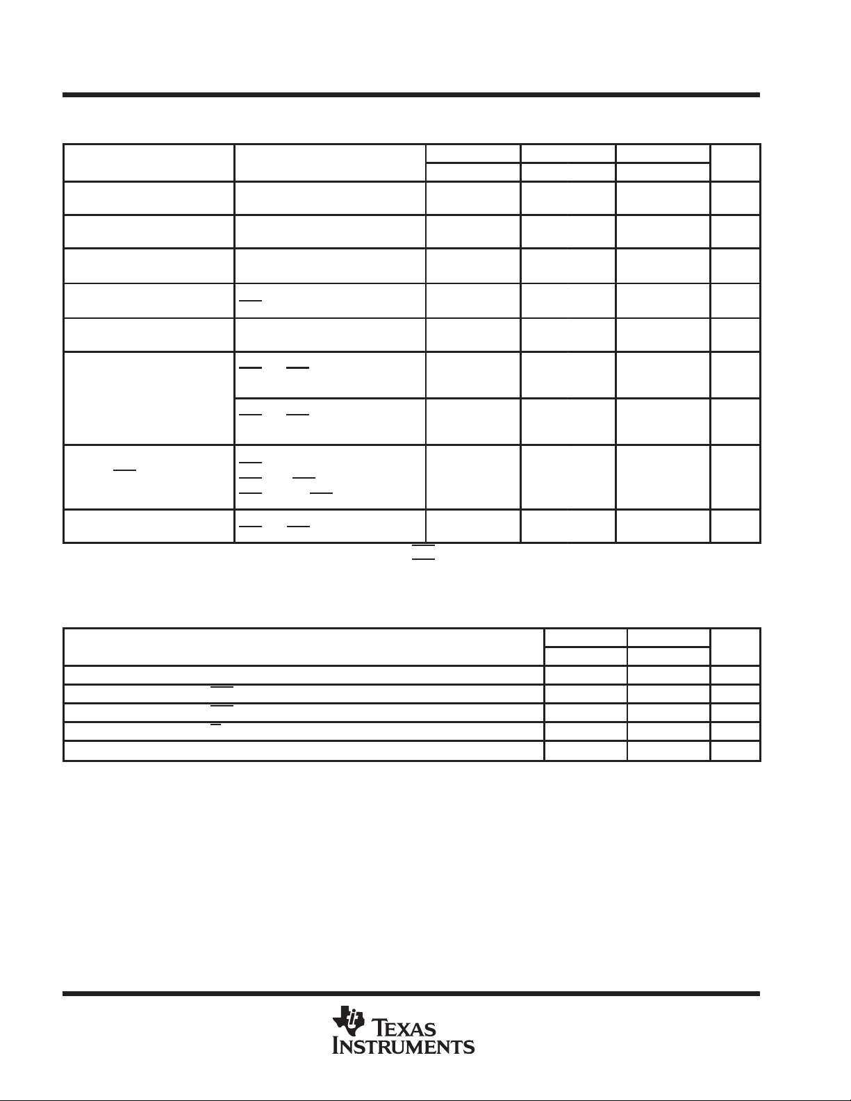
The TM124MBK36B operates as eight TMS44400DJs and one TMS44460DJ connected as shown in the
functional block diagram and Table 1. The parity bits are provided by the TMS44460DJ and are controlled by
RAS2
. To ensure proper parity bit operation all memory accesses should include a RAS2 pulse. Refer to the
TMS44400 and TMS44460 data sheets for details of operation. The common I/O feature dictates the use of
early write cycles to prevent contention on D and Q.
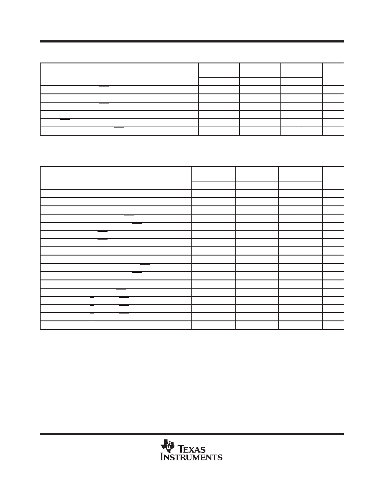
TM248NBK36B
The TM248NBK36B operates as sixteen TMS44400DJs and two TMS44460DJs connected as shown in the
functional block diagram and Table 1. The parity bits are provided by the TMS44460DJ and are controlled by
RAS2
on side 1 and RAS3 on side 2. T o ensure proper parity bit operation, all memory accesses should include
a RAS2
common I/O feature dictates the use of early write cycles to prevent contention on D and Q.
or RAS3 pulse. Refer to the TMS44400 and TMS44460 data sheets for details of operation. The
2
POST OFFICE BOX 1443 • HOUSTON, TEXAS 77251–1443
TM124MBK36B, TM124MBK36R 1048576 BY 36-BIT
TM248NBK36B, TM248NBK36R 2097152 BY 36-BIT
DYNAMIC RAM MODULE
SMMS137E – JANUARY 1991 – REVISEDJUNE 1995
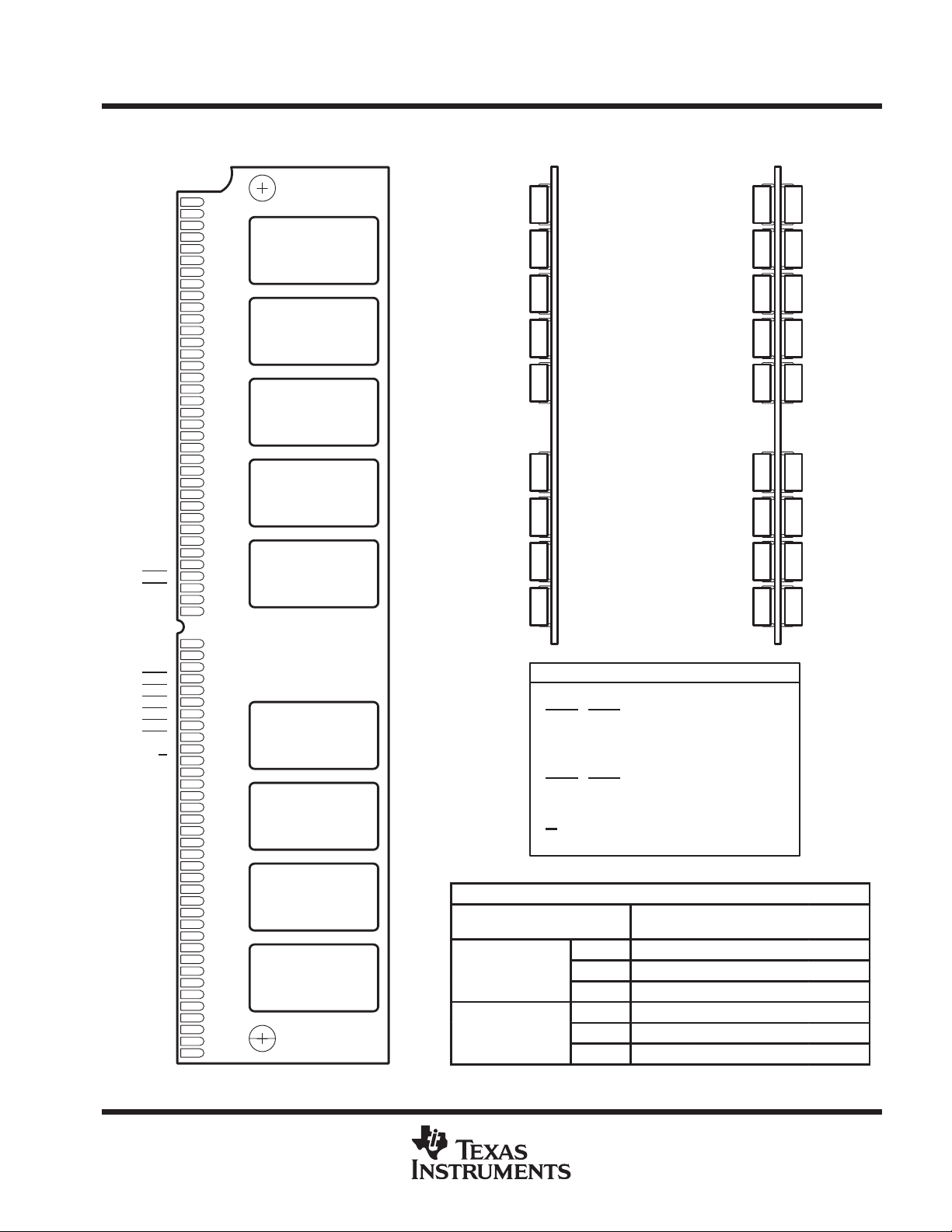
BK SINGLE IN-LINE MEMORY MODULE
(TOP VIEW)
V
SS
DQ0
DQ18
DQ1
DQ19
DQ2
DQ20
DQ3
DQ21
V
CC
NC
NC
DQ4
DQ22
DQ5
DQ23
DQ6
DQ24
DQ7
DQ25
NC
V
CC
RAS3
RAS2
DQ26
DQ8
A0
A1
A2
A3
A4
A5
A6
A7
A8
A9
1
2
3
4
5
6
7
8
9
10
11
12
13
14
15
16
17
18
19
20
21
22
23
24
25
26
27
28
29
30
31
32
33
34
35
36
TM124MBK36B
(SIDE VIEW)
TM248NBK36B
(SIDE VIEW)
DQ17
DQ35
V
SS
CAS0
CAS2
CAS3
CAS1
RAS0
RAS1
NC
NC
DQ9
DQ27
DQ10
DQ28
DQ11
DQ29
DQ12
DQ30
DQ13
DQ31
V
CC
DQ32
DQ14
DQ33
DQ15
DQ34
DQ16
NC
PD1
PD2
PD3
PD4
NC
V
SS
37
38
39
40
41
42
43
44
45
W
46
47
48
49
50
51
52
53
54
55
56
57
58
59
60
61
62
63
64
65
66
67
68
69
70
71
72
TM124MBK36B
TM248NBK36B
A0–A9 Address Inputs
CAS0
DQ0–DQ35 Data In/Data Out
NC No Connection
PD1– PD4 Presence Detects
RAS0
V
V
W
SIGNAL
(PIN)
PIN NOMENCLATURE
–CAS3 Column-Address Strobe
–RAS3 Row-Address Strobe
CC
SS
5-V Supply
Ground
Write Enable
PRESENCE DETECT
80 ns V
70 ns V
60 ns V
PD1
(67)
SS
SS
SS
PD2
(68)
V
SS
V
SS
V
SS
PD3
(69)
NC V
V
NC NC
80 ns NC NC NC V
70 ns NC NC V
60 ns NC NC NC NC
SS
SS
PD4
(70)
SS
NC
SS
NC
POST OFFICE BOX 1443 • HOUSTON, TEXAS 77251–1443
3
TM124MBK36B, TM124MBK36R 1048576 BY 36-BIT
DATA BLOCK
CASx
TM248NBK36B, TM248NBK36R 2097152 BY 36-BIT
DYNAMIC RAM MODULE
SMMS137E – JANUARY 1991 – REVISEDJUNE 1995
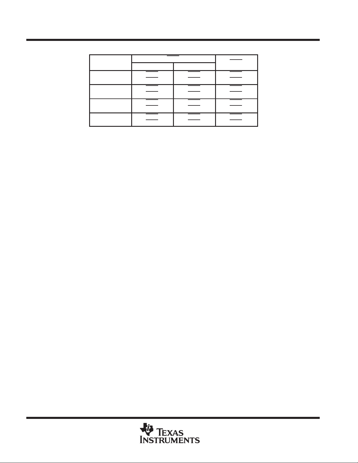
Table 1. Connection Table
RASx
RAS1
RAS3
RAS1
RAS3
RAS3
RAS3
RAS3
RAS3
†
CAS0
CAS0
CAS1
CAS1
CAS2
CAS2
CAS3
CAS3
SIDE 1 SIDE 2
DQ0–DQ7
DQ8
DQ9–DQ16
DQ17
DQ18–DQ25
DQ26
DQ27–DQ34
DQ35
†
Side 2 applies to the TM248NBK36B only.
RAS0
RAS2
RAS0
RAS2
RAS2
RAS2
RAS2
RAS2
single-in-line memory module and components
PC substrate: 1,27 ± 0,1 mm (0.05 inch) nominal thickness; 0.005 inch/inch maximum warpage
Bypass capacitors: Multilayer ceramic
Contact area for TM124MBK36B and TM248NBK36B: Nickel plate and gold plate over copper
Contact area for TM124MBK36R and TM248NBK36R: Nickel plate and tin-lead over copper
4
POST OFFICE BOX 1443 • HOUSTON, TEXAS 77251–1443

DQ27–
TM124MBK36B, TM124MBK36R 1048576 BY 36-BIT
TM248NBK36B, TM248NBK36R 2097152 BY 36-BIT
DYNAMIC RAM MODULE
DQ35
DQ26
DQ17
DQ8
DQ30
DQ31–
SMMS137E – JANUARY 1991 – REVISED JUNE 1995
DQ34
RAS2
CAS3
DQ4
1M × 4
A0–A9
RAS
1M × 4
A0–A9
RAS
DQ1–
W
CAS
OE
DQ18–
DQ4
DQ1–
W
CAS
OE
DQ9–
DQ21
DQ12
1M × 4
A0–A9
RAS
W
1M × 4
A0–A9
RAS
W
CAS
CAS
OE
OE
DQ4
DQ1–
DQ22–
DQ4
DQ1–
DQ13–
DQ25
DQ16
1M × 4
10
A0–A9
RAS
W
CAS4 DQ4
CAS3 DQ3
CAS2 DQ2
CAS1 DQ1
OE
DQ4
1M × 4
A0–A9
RAS
10 10 10
1M × 4
A0–A9
RAS
10
10
W
RAS0
functional block diagram (TM124MBK36B and TM248NBK36B, side 1)
A0–A9
CAS0 CAS1 CAS2
DQ1–
W
CAS
OE
DQ0–
DQ4
DQ1–
W
CAS
OE
DQ3
10 10 10 10
1M × 4
A0–A9
RAS
W
1M × 4
A0–A9
RAS
W
CAS
CAS
OE
OE
DQ4
DQ1–
DQ4–
DQ7
DQ4
DQ1–
POST OFFICE BOX 1443 HOUSTON, TEXAS 77251–1443
• 5

T
emplate Release Date: 7–11–
94
TM124MBK36B, TM124MBK36R 1048576 BY 36-BIT
TM248NBK36B, TM248NBK36R 2097152 BY 36-BIT
DYNAMIC RAM MODULE
SMMS137E – JANUARY 1991 – REVISED JUNE 1995
DQ27–
DQ30
DQ31–
DQ34
DQ35
DQ26
DQ17
DQ8
RAS3
CAS3
DQ4
1M × 4
A0–A9
RAS
1M × 4
A0 –A9
RAS
DQ1–
W
CAS
OE
DQ18 –
DQ4
DQ1–
W
CAS
OE
DQ9–
DQ21
DQ12
1M × 4
A0–A9
RAS
W
1M × 4
A0 –A9
RAS
W
CAS
CAS
OE
OE
DQ4
DQ1–
DQ22–
DQ4
DQ1–
DQ13–
DQ25
DQ16
1M × 4
10
A0 –A9
RAS
W
CAS4 DQ4
CAS3 DQ3
CAS2 DQ2
CAS1 DQ1
OE
DQ4
1M × 4
A0 –A9
RAS
10 10 10
1M × 4
A0 –A9
RAS
10
10
W
RAS1
functional block diagram (TM248NBK36B, side 2)
A0 –A9
CAS0 CAS1 CAS2
DQ1–
W
CAS
OE
DQ0 –
DQ3
DQ4
DQ1–
W
CAS
OE
10 10 10 10
DQ4
1M × 4
A0 –A9
RAS
1M × 4
A0 –A9
RAS
DQ1–
W
CAS
OE
DQ4–
DQ7
DQ4
DQ1–
W
CAS
OE
6
POST OFFICE BOX 1443 HOUSTON, TEXAS 77251–1443
•

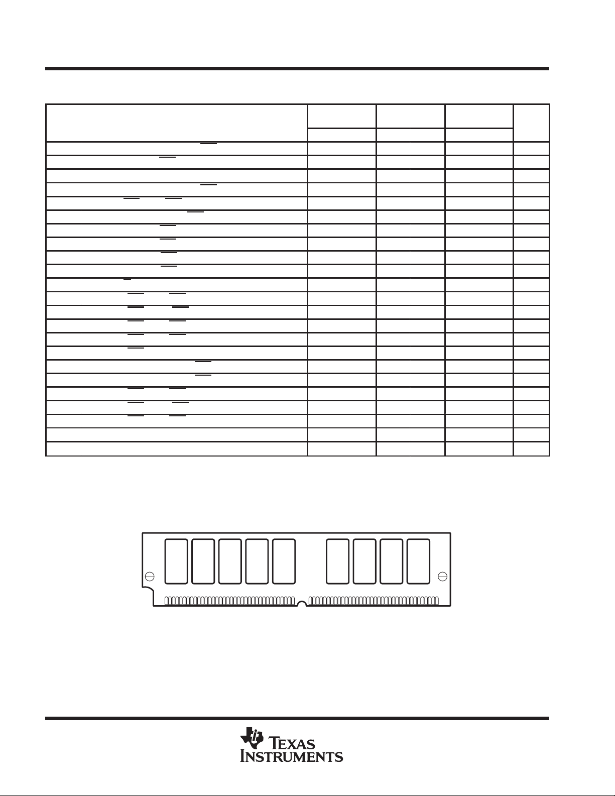
PARAMETER
TEST CONDITIONS
UNIT
I
Standby current
TM124MBK36B, TM124MBK36R 1048576 BY 36-BIT
TM248NBK36B, TM248NBK36R 2097152 BY 36-BIT
DYNAMIC RAM MODULE
SMMS137E – JANUARY 1991 – REVISEDJUNE 1995
absolute maximum ratings over operating free-air temperature range (unless otherwise noted)
†
Voltage range on any pin (see Note 1) – 1 V to 7 V. . . . . . . . . . . . . . . . . . . . . . . . . . . . . . . . . . . . . . . . . . . . . . . . .
Voltage range on V
(see Note 1) – 1 V to 7 V. . . . . . . . . . . . . . . . . . . . . . . . . . . . . . . . . . . . . . . . . . . . . . . . . .
CC
Short-circuit output current 50 mA. . . . . . . . . . . . . . . . . . . . . . . . . . . . . . . . . . . . . . . . . . . . . . . . . . . . . . . . . . . . . . . .
Power dissipation 9 W. . . . . . . . . . . . . . . . . . . . . . . . . . . . . . . . . . . . . . . . . . . . . . . . . . . . . . . . . . . . . . . . . . . . . . . . . .
Operating free-air temperature range, T
Storage temperature range, T
†
Stresses beyond those listed under “absolute maximum ratings” may cause permanent damage to the device. These are stress ratings only, and
functional operation of the device at these or any other conditions beyond those indicated under “recommended operating conditions” is not
implied. Exposure to absolute-maximum-rated conditions for extended periods may affect device reliability.
NOTE 1: All voltage values are with respect to VSS.
–55°C to 125°C. . . . . . . . . . . . . . . . . . . . . . . . . . . . . . . . . . . . . . . . . . . . . . . . . .
stg
0°C to 70°C. . . . . . . . . . . . . . . . . . . . . . . . . . . . . . . . . . . . . . . . . . . . . .
A
recommended operating conditions
MIN NOM MAX UNIT
V
Supply voltage 4.5 5 5.5 V
CC
V
High-level input voltage 2.4 6.5 V
IH
V
Low-level input voltage (see Note 2) – 1 0.8 V
IL
T
Operating free-air temperature 0 70 °C
A
NOTE 2: The algebraic convention, where the more negative (less positive) limit is designated as minimum, is used for logic-voltage levels only.
electrical characteristics over recommended ranges of supply voltage and operating free-air
temperature (unless otherwise noted)
’124MBK36B-60 ’124MBK36B-70 ’124MBK36B-80
MIN MAX MIN MAX MIN MAX
High-level output
V
OH
voltage
Low-level output
V
OL
voltage
I
Input current (leakage)
I
Output current
I
O
(leakage)
Read or write cycle
I
CC1
current (see Note 3)
CC2
Average refresh current
(RAS
I
CC3
I
CC4
NOTES: 3. Measured with a maximum of one address change while RAS = V
only or CBR)
(see Note 3)
Average page current
(see Note 4)
4. Measured with a maximum of one address change while CAS
IOH = – 5 mA 2.4 2.4 2.4 V
IOL = 4.2 mA 0.4 0.4 0.4 V
VCC = 5.5 V, VI = 0 V to 6.5 V,
All other pins = 0 V to V
VCC = 5.5 V, VO = 0 V to VCC,
high
CAS
VCC = 5.5 V, Minimum cycle 945 810 720 mA
After 1 memory cycle,
RAS
and CAS high,
VIH = 2.4 V (TTL)
After 1 memory cycle,
RAS
and CAS high,
VIH = VCC – 0.2 V (CMOS)
VCC = 5.5 V, Minimum cycle,
cycling,
RAS
high (RAS only),
CAS
low after CAS low (CBR)
RAS
VCC = 5.5 V, tPC = minimum,
low, CAS cycling
RAS
CC
= V
± 10 ±10 ± 10 µA
± 10 ±10 ± 10 µA
18 18 18 mA
9 9 9 mA
945 810 720 mA
810 720 630 mA
IL
IH
POST OFFICE BOX 1443 • HOUSTON, TEXAS 77251–1443
7
TM124MBK36B, TM124MBK36R 1048576 BY 36-BIT
PARAMETER
TEST CONDITIONS
UNIT
I
Standby current
PARAMETER
UNIT
TM248NBK36B, TM248NBK36R 2097152 BY 36-BIT
DYNAMIC RAM MODULE
SMMS137E – JANUARY 1991 – REVISEDJUNE 1995
electrical characteristics over recommended ranges of supply voltage and operating free-air
temperature (unless otherwise noted)
’248NBK36B-60 ’248NBK36B-70 ’248NBK36B-80
MIN MAX MIN MAX MIN MAX
High-level output
V
OH
voltage
Low-level output
V
OL
voltage
I
Input current (leakage)
I
Output current
I
O
(leakage)
Read or write cycle
I
CC1
current (see Note 3)
CC2
Average refresh current
(RAS
I
CC3
I
CC4
NOTES: 3. Measured with a maximum of one address change while RAS = V
only or CBR)
(see Note 3)
Average page current
(see Note 4)
4. Measured with a maximum of one address change while CAS
IOH = – 5 mA 2.4 2.4 2.4 V
IOL = 4.2 mA 0.4 0.4 0.4 V
VCC = 5.5 V, VI = 0 V to 6.5 V,
All other pins = 0 V to V
VCC = 5.5 V, VO = 0 V to VCC,
high
CAS
VCC = 5.5 V, Minimum cycle 963 828 738 mA
After 1 memory cycle,
RAS
and CAS high,
VIH = 2.4 V (TTL)
After 1 memory cycle,
RAS
and CAS high,
VIH = VCC – 0.2 V (CMOS)
VCC = 5.5 V, Minimum cycle,
cycling,
RAS
high (RAS only),
CAS
low after CAS low (CBR)
RAS
VCC = 5.5 V, tPC = minimum,
low, CAS cycling
RAS
CC
= V
± 20 ± 20 ± 20 µA
± 20 ± 20 ± 20 µA
36 36 36 mA
18 18 18 mA
1890 1620 1440 mA
828 738 648 mA
IL
IH
capacitance over recommended ranges of supply voltage and operating free-air temperature,
f = 1 MHz (see Note 5)
’124MBK36B ’248NBK36B
MIN MAX MIN MAX
C
i(A)
C
i(R)
C
i(C)
C
i(W)
C
o(DQ)
NOTE 5: VCC = 5 V ± 0.5 V and the bias on pins under test is 0 V.
Input capacitance, A0–A9 45 90 pF
Input capacitance, RAS 35 35 pF
Input capacitance, CAS 21 42 pF
Input capacitance, W 63 126 pF
Output capacitance on DQ pins 7 14 pF
8
POST OFFICE BOX 1443 • HOUSTON, TEXAS 77251–1443
TM124MBK36B, TM124MBK36R 1048576 BY 36-BIT
TM248NBK36B, TM248NBK36R 2097152 BY 36-BIT
DYNAMIC RAM MODULE
SMMS137E – JANUARY 1991 – REVISEDJUNE 1995
switching characteristics over recommended ranges of supply voltage and operating free-air
temperature
’124MBK36B-60
’248NBK36B-60
MIN MAX MIN MAX MIN MAX
t
CAC
t
AA
t
RAC
t
CPA
t
CLZ
t
OFF
NOTE 6: t
PARAMETER
Access time from CAS low 15 18 20 ns
Access time from column address 30 35 40 ns
Access time from RAS low 60 70 80 ns
Access time from column precharge 35 40 45 ns
CAS to output in low impedance 0 0 0 ns
Output disable time after CAS high (see Note 6) 0 15 0 18 0 20 ns
is specified when the output is no longer driven.
OFF
timing requirements over recommended ranges of supply voltage and operating free-air
temperature
’124MBK36B-60
’248NBK36B-60
MIN MAX MIN MAX MIN MAX
t
RC
t
RWC
t
PC
t
RASP
t
RAS
t
CAS
t
CP
t
RP
t
WP
t
ASC
t
ASR
t
DS
t
RCS
t
CWL
t
RWL
t
WCS
t
WSR
NOTES: 7. All cycles assume tT = 5 ns.
Cycle time, random read or write (see Note 7) 110 130 150 ns
Cycle time, read write 130 153 175 ns
Cycle time, page-mode read or write (see Note 8) 40 45 50 ns
Pulse duration, page mode, RAS low 60 100 000 70 100 000 80 100 000 ns
Pulse duration, nonpage mode, RAS low 60 10 000 70 10 000 80 10 000 ns
Pulse duration, CAS low 15 10 000 18 10 000 20 10 000 ns
Pulse duration, CAS high 10 10 10 ns
Pulse duration, RAS high (precharge) 40 50 60 ns
Pulse duration, write 15 15 15 ns
Setup time, column address before CAS low 0 0 0 ns
Setup time, row address before RAS low 0 0 0 ns
Setup time, data 0 0 0 ns
Setup time, read before CAS low 0 0 0 ns
Setup time, W low before CAS high 15 18 20 ns
Setup time, W low before RAS high 15 18 20 ns
Setup time, W low before CAS low 0 0 0 ns
Setup time, W high (see Note 9) 10 10 10 ns
8. To assure tPC min, t
9. CBR refresh only
should be ≥ 5 ns.
ASC
’124MBK36B-70
’248NBK36B-70
’124MBK36B-70
’248NBK36B-70
’124MBK36B-80
’248NBK36B-80
’124MBK36B-80
’248NBK36B-80
UNIT
UNIT
POST OFFICE BOX 1443 • HOUSTON, TEXAS 77251–1443
9
TM124MBK36B, TM124MBK36R 1048576 BY 36-BIT
TM248NBK36B, TM248NBK36R 2097152 BY 36-BIT
DYNAMIC RAM MODULE
SMMS137E – JANUARY 1991 – REVISEDJUNE 1995
timing requirements over recommended ranges of supply voltage and operating free-air
temperature (continued)
t
CAH
t
DHR
t
DH
t
AR
t
CLCH
t
RAH
t
RCH
t
RRH
t
WCH
t
WCR
t
WHR
t
CHR
t
CRP
t
CSH
t
CSR
t
RAD
t
RAL
t
CAL
t
RCD
t
RPC
t
RSH
t
REF
t
T
NOTES: 9. CBR refresh only
Hold time, column address after CAS low 10 15 15 ns
Hold time, data after RAS low (see Note 10) 50 55 60 ns
Hold time, data 10 15 15 ns
Hold time, column address after RAS low (see Note 10) 50 55 60 ns
Hold time, CAS low to CAS high 5 5 5 ns
Hold time, row address after RAS low 10 10 10 ns
Hold time, read after CAS high (see Note 11) 0 0 0 ns
Hold time, read after RAS high (see Note 11) 0 0 0 ns
Hold time, write after CAS low 15 15 15 ns
Hold time, write after RAS low (see Note 10) 50 55 60 ns
Hold time, W high (see Note 9) 10 10 10 ns
Delay time, RAS low to CAS high (see Note 9) 15 15 20 ns
Delay time, CAS high to RAS low 0 0 0 ns
Delay time, RAS low to CAS high 60 70 80 ns
Delay time, CAS low to RAS low (see Note 9) 10 10 10 ns
Delay time, RAS low to column address (see Note 12) 15 30 15 35 15 40 ns
Delay time, column address to RAS high 30 35 40 ns
Delay time, column address to CAS high 30 35 40 ns
Delay time, RAS low to CAS low (see Note 12) 20 45 20 52 20 60 ns
Delay time, RAS high to CAS low (see Note 9) 0 0 0 ns
Delay time, CAS low to RAS high 15 18 20 ns
Refresh time interval 16 16 16 ms
Transition time 2 50 2 50 2 50 ns
10. The minimum value is measured when t
11. Either t
12. The maximum value is specified only to assure access time.
RRH
or t
must be satisfied for a read cycle.
RCH
RCD
is set to t
’124MBK36B-60
’248NBK36B-60
MIN MAX MIN MAX MIN MAX
min as a reference.
RCD
’124MBK36B-70
’248NBK36B-70
’124MBK36B-80
’248NBK36B-80
UNIT
device symbolization (TM124MBK36B illustrated)
TM124MBK36B
YY = Year Code
MM = Month Code
T = Assembly Site Code
–SS = Speed Code
NOTE: Location of symbolization may vary.
10
POST OFFICE BOX 1443 • HOUSTON, TEXAS 77251–1443
–SS YYMMT

IMPORTANT NOTICE
T exas Instruments and its subsidiaries (TI) reserve the right to make changes to their products or to discontinue
any product or service without notice, and advise customers to obtain the latest version of relevant information
to verify, before placing orders, that information being relied on is current and complete. All products are sold
subject to the terms and conditions of sale supplied at the time of order acknowledgement, including those
pertaining to warranty, patent infringement, and limitation of liability.
TI warrants performance of its semiconductor products to the specifications applicable at the time of sale in
accordance with TI’s standard warranty. Testing and other quality control techniques are utilized to the extent
TI deems necessary to support this warranty . Specific testing of all parameters of each device is not necessarily
performed, except those mandated by government requirements.
CERT AIN APPLICATIONS USING SEMICONDUCTOR PRODUCTS MAY INVOLVE POTENTIAL RISKS OF
DEATH, PERSONAL INJURY, OR SEVERE PROPERTY OR ENVIRONMENTAL DAMAGE (“CRITICAL
APPLICATIONS”). TI SEMICONDUCTOR PRODUCTS ARE NOT DESIGNED, AUTHORIZED, OR
WARRANTED TO BE SUITABLE FOR USE IN LIFE-SUPPORT DEVICES OR SYSTEMS OR OTHER
CRITICAL APPLICA TIONS. INCLUSION OF TI PRODUCTS IN SUCH APPLICATIONS IS UNDERST OOD TO
BE FULLY AT THE CUSTOMER’S RISK.
In order to minimize risks associated with the customer’s applications, adequate design and operating
safeguards must be provided by the customer to minimize inherent or procedural hazards.
TI assumes no liability for applications assistance or customer product design. TI does not warrant or represent
that any license, either express or implied, is granted under any patent right, copyright, mask work right, or other
intellectual property right of TI covering or relating to any combination, machine, or process in which such
semiconductor products or services might be or are used. TI’s publication of information regarding any third
party’s products or services does not constitute TI’s approval, warranty or endorsement thereof.
Copyright 1999, Texas Instruments Incorporated
 Loading...