

www.ti.com
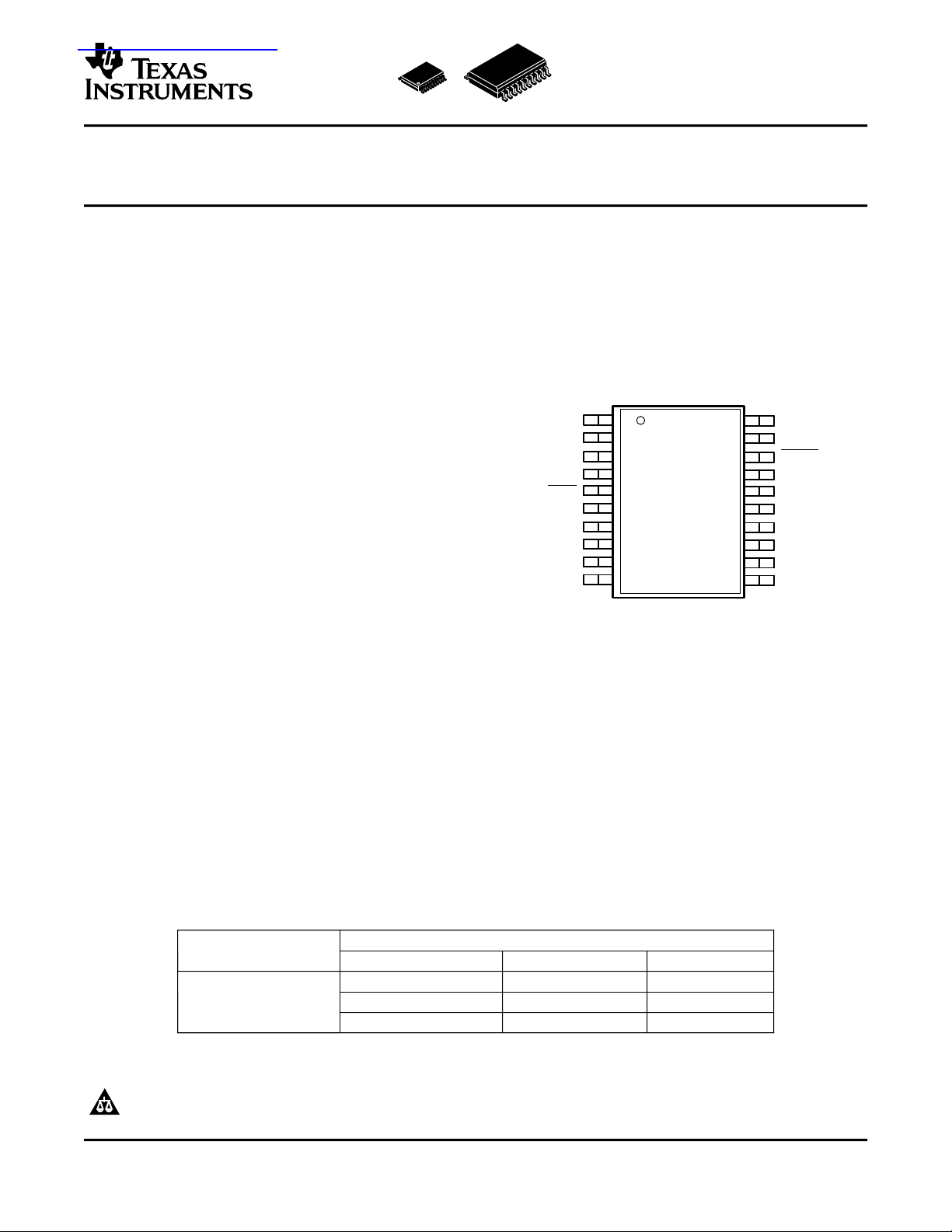
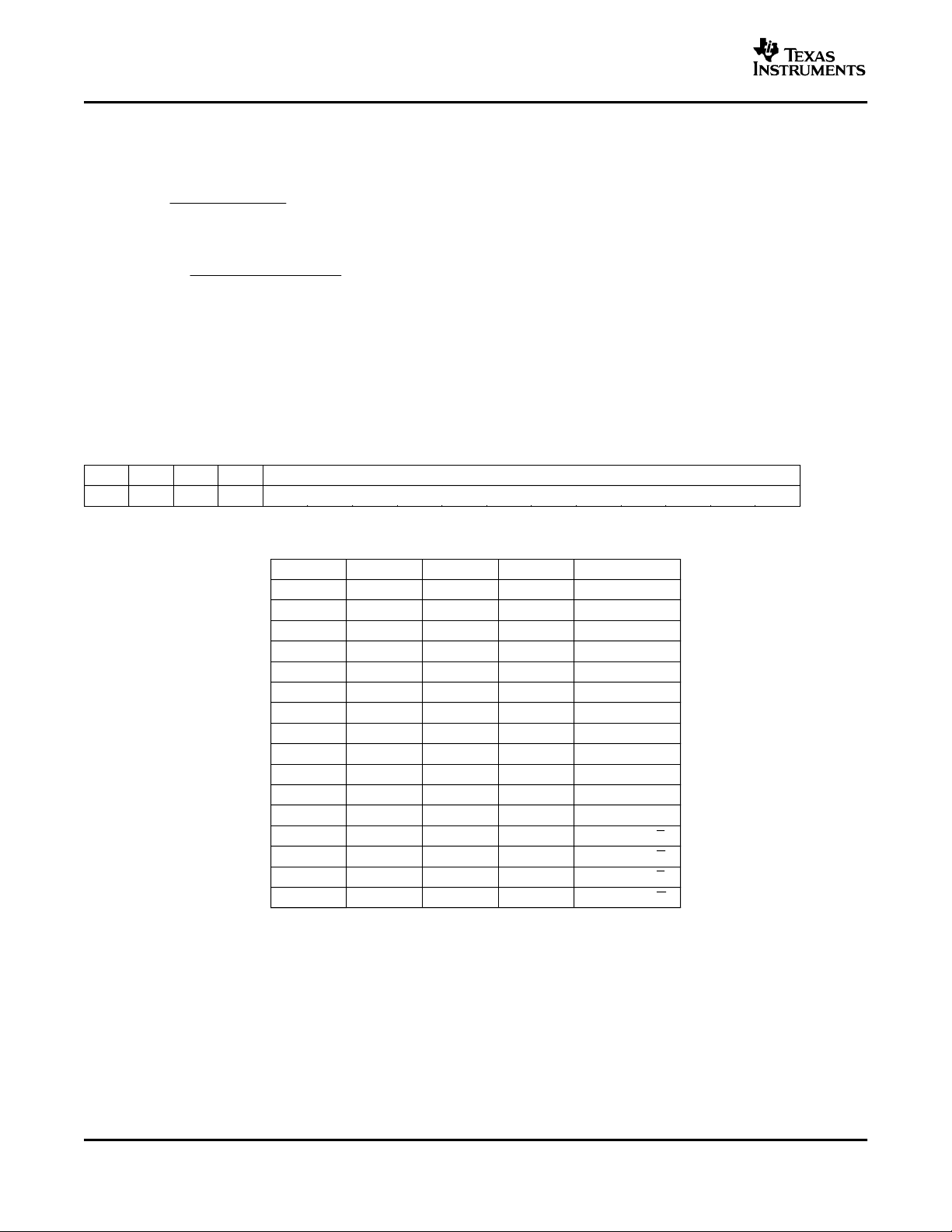
1
2
3
4
5
6
7
8
9
10
20
19
18
17
16
15
14
13
12
11
DGND
DIN
SCLK
FS
PRE
OUTE
OUTF
OUTG
OUTH
AGND
DV
DD
DOUT
LDAC
MODE
REF
OUTD
OUTC
OUTB
OUTA
AV
DD
DW OR PW PACKAGE
(TOP VIEW)
查询TLV5608IDW供应商
8-CHANNEL, 12-/10-/8-BIT, 2.7-V TO 5.5-V LOW POWER
DIGITAL-TO-ANALOG CONVERTER WITH POWER DOWN
FEATURES APPLICATIONS
• Eight Voltage Output DACs in One Package
– TLV5610 . . . 12-Bit
– TLV5608 . . . 10-Bit
– TLV5629 . . . 8-Bit
• Programmable Settling Time vs Power
Consumption
– 1 µs In Fast Mode
– 3 µs In Slow Mode
• Compatible With TMS320 and SPI™ Serial
Ports
• Monotonic Over Temperature
• Low Power Consumption:
– 18 mW In Slow Mode at 3-V
– 48 mW In Fast Mode at 3-V
• Reference Input Buffers
• Power-Down Mode
• Buffered, High Impedance Reference Inputs
• Data Output for Daisy-Chaining
TLV5608
TLV5610
TLV5629
SLAS268E – MAY 2000 – REVISED MARCH 2004
• Digital Servo Control Loops
• Digital Offset and Gain Adjustment
• Industrial Process Control
• Machine and Motion Control Devices
• Mass Storage Devices
DESCRIPTION
The TLV5610, TLV5608, and TLV5629 are pin-compatible, eight-channel, 12-/10-/8-bit voltage output DACs
each with a flexible serial interface. The serial interface allows glueless interface to TMS320 and SPI, QSPI, and
Microwire serial ports. It is programmed with a 16-bit serial string containing 4 control and 12 data bits.
Additional features are a power-down mode, an LDAC input for simultaneous update of all eight DAC outputs,
and a data output which can be used to cascade multiple devices.
The resistor string output voltage is buffered by a rail-to-rail output amplifier with a programmable settling time to
allow the designer to optimize speed vs power dissipation. The buffered, high-impedance reference input can be
connected to the supply voltage.
Implemented with a CMOS process, the DACs are designed for single-supply operation from 2.7 V to 5.5 V. The
devices are available in 20-pin SOIC and TSSOP packages.
AVAILABLE OPTIONS
PACKAGE
Copyright © 2000–2004, Texas Instruments Incorporated
SPI is a trademark of Motorola, Inc.
PRODUCTION DATA information is current as of publication date.
Products conform to specifications per the terms of the Texas
Instruments standard warranty. Production processing does not
necessarily include testing of all parameters.
Please be aware that an important notice concerning availability, standard warranty, and use in critical applications of Texas
Instruments semiconductor products and disclaimers thereto appears at the end of this data sheet.
-40°C to 85°C TLV5608IDW TLV5608IPW 10
T
A
SMALL OUTLINE (DW) TSSOP (PW) RESOLUTION
TLV5610IDW TLV5610IPW 12
TLV5629IDW TLV5629IPW 8
www.ti.com
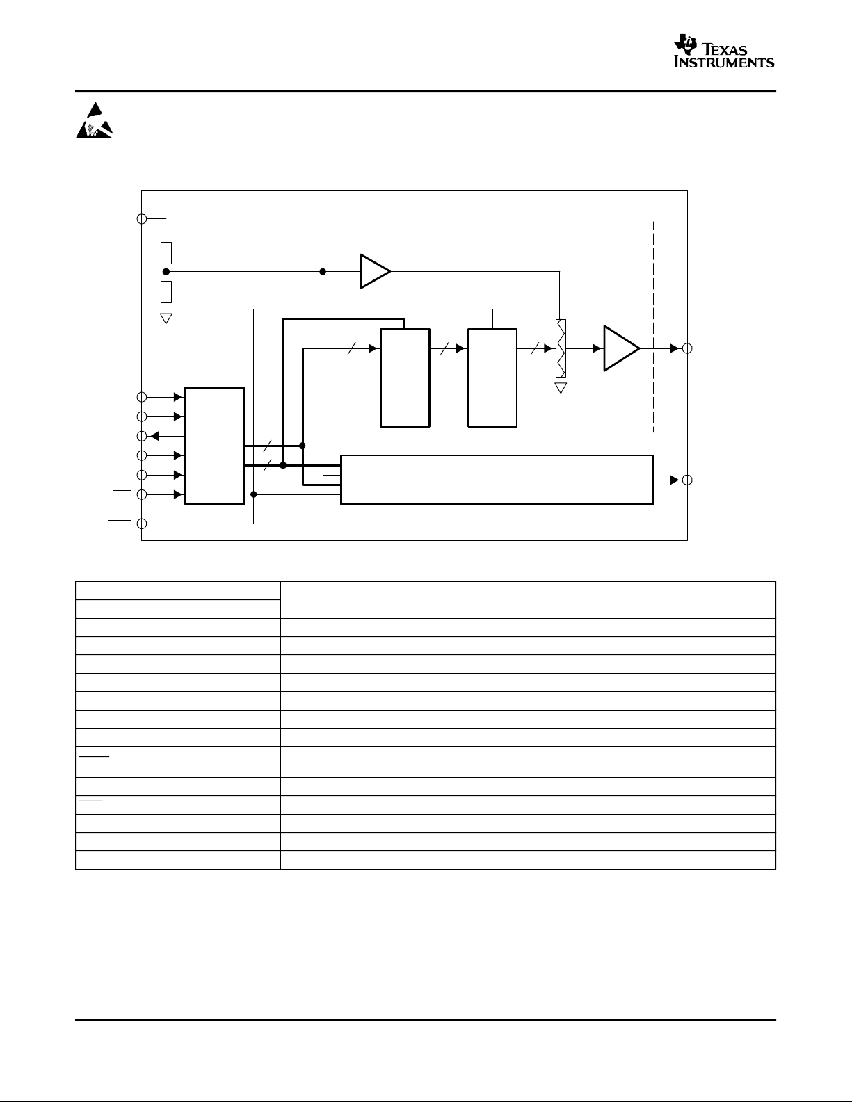
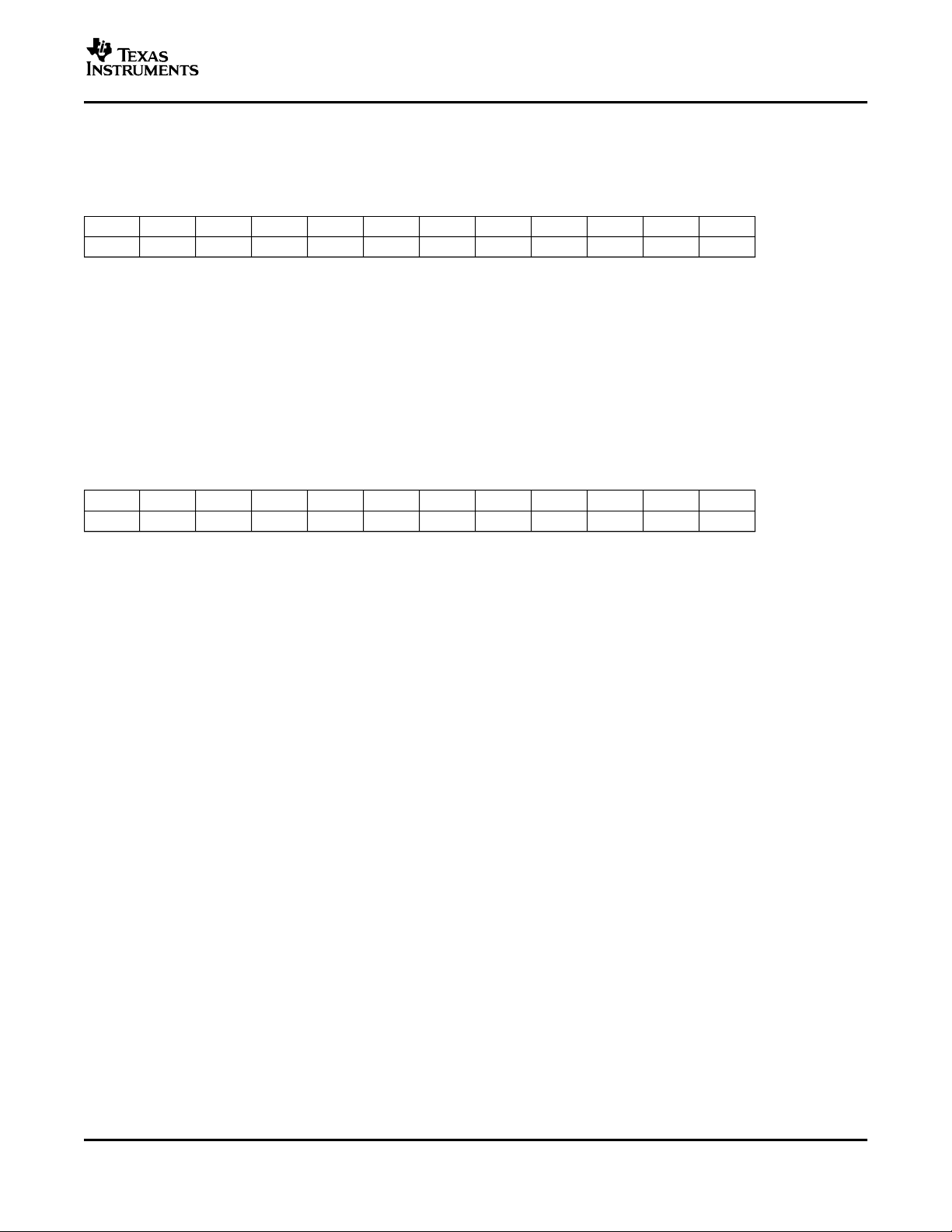
OUTA
12/10/8
12/10/8
Serial
Interface
12
8
REF
SCLK
DIN
FS
MODE
DOUT
DAC B, C, D, E, F, G and H
Same as DAC A
OUT
PRE
LDAC
X2
B, C, D,
E, F, G
and H
DAC A
Holding
Latch
DAC A
Latch
12/10/8
TLV5608
TLV5610
TLV5629
SLAS268E – MAY 2000 – REVISED MARCH 2004
These devices have limited built-in ESD protection. The leads should be shorted together or the device placed in conductive foam
during storage or handling to prevent electrostatic damage to the MOS gates.
FUNCTIONAL BLOCK DIAGRAM
Terminal Functions
TERMINAL
NAME NO.
AGND 10 I Analog ground
AV
DD
11 I Analog power supply
DGND 1 I Digital ground
DIN 2 I Digital serial data input
DOUT 19 O Digital serial data output
DV
DD
20 I Digital power supply
FS 4 I Frame sync input
LDAC 18 I
MODE 17 I DSP/µC mode pin. High = µC mode, NC = DSP mode.
PRE 5 I Preset input
REF 16 I Voltage reference input
SCLK 3 I Serial clock input
OUTA-OUTH 6-9, 12-15 O DAC outputs A, B, C, D, E, F, G and H
2
I/O DESCRIPTION
Load DAC. The DAC outputs are only updated, if this signal is low. It is an
asynchronous input.
www.ti.com
TLV5608
TLV5610
TLV5629
SLAS268E – MAY 2000 – REVISED MARCH 2004
ABSOLUTE MAXIMUM RATINGS
over operating free-air temperature range (unless otherwise noted)
Supply voltage (AV
Reference input voltage - 0.3 V to AV
Digital input voltage range - 0.3 V to DV
Operating free-air temperature range, T
Storage temperature range, T
Lead temperature 1,6 mm (1/16 inch) from case for 10 seconds 260°C
(1) Stresses beyond those listed under absolute maximum ratings may cause permanent damage to the device. These are stress ratings
only, and functional operation of the device at these or any other conditions beyond those indicated under recommended operating
conditions is not implied. Exposure to absolute-maximum-rated conditions for extended periods may affect device reliability.
, DV
DD
to GND) 7 V
DD
A
stg
(1)
UNIT
+ 0.3 V
DD
+ 0.3 V
DD
-40°C to 85°C
-65°C to 150°C
RECOMMENDED OPERATING CONDITIONS
MIN NOM MAX UNIT
Supply voltage, AV
High-level digital input voltage, V
Low-level digital input voltage, V
Reference voltage, V
Load resistance, R
Load capacitance, C
Clock frequency, f
Operating free-air temperature, T
, DV
DD
DD
5-V operation 4.5 5 5.5 V
3-V operation 2.7 3 3.3 V
DV
= 2.7 V 2
IH
IL
ref
L
L
CLK
A
DD
DV
= 5.5 V 2.4
DD
DV
= 2.7 V 0.6
DD
DV
= 5.5 V 1
DD
AV
= 5 V GND 4.096 AV
DD
AV
= 3 V GND 2.048 AV
DD
2 kΩ
-40 85 °C
DD
DD
100 pF
30 MHz
V
V
V
V
ELECTRICAL CHARACTERISTICS
over recommended operating free-air temperature range, supply voltages, and reference voltages (unless otherwise noted)
POWER SUPPLY
PARAMETER TEST CONDITIONS MIN TYP MAX UNIT
I
DD
Power supply current mA
No load, V
All inputs = DV
ref
= 4.096 V,
DD
or GND
Power down supply current 0.1 µA
POR Power on threshold 2 V
PSRR Power supply rejection ratio Full scale
(1)
(1) Power supply rejection ratio at full scale is measured by varying AV
PSRR = 20 log [(E
(AV
max) - EG(AV
G
DD
min))/V
DD
max]
DD
Fast 16 21
Slow 6 8
and is given by:
DD
-60 dB
3
www.ti.com
TLV5608
TLV5610
TLV5629
SLAS268E – MAY 2000 – REVISED MARCH 2004
ELECTRICAL CHARACTERISTICS (CONTINUED)
over recommended operating free-air temperature range, supply voltages, and reference voltages (unless otherwise noted)
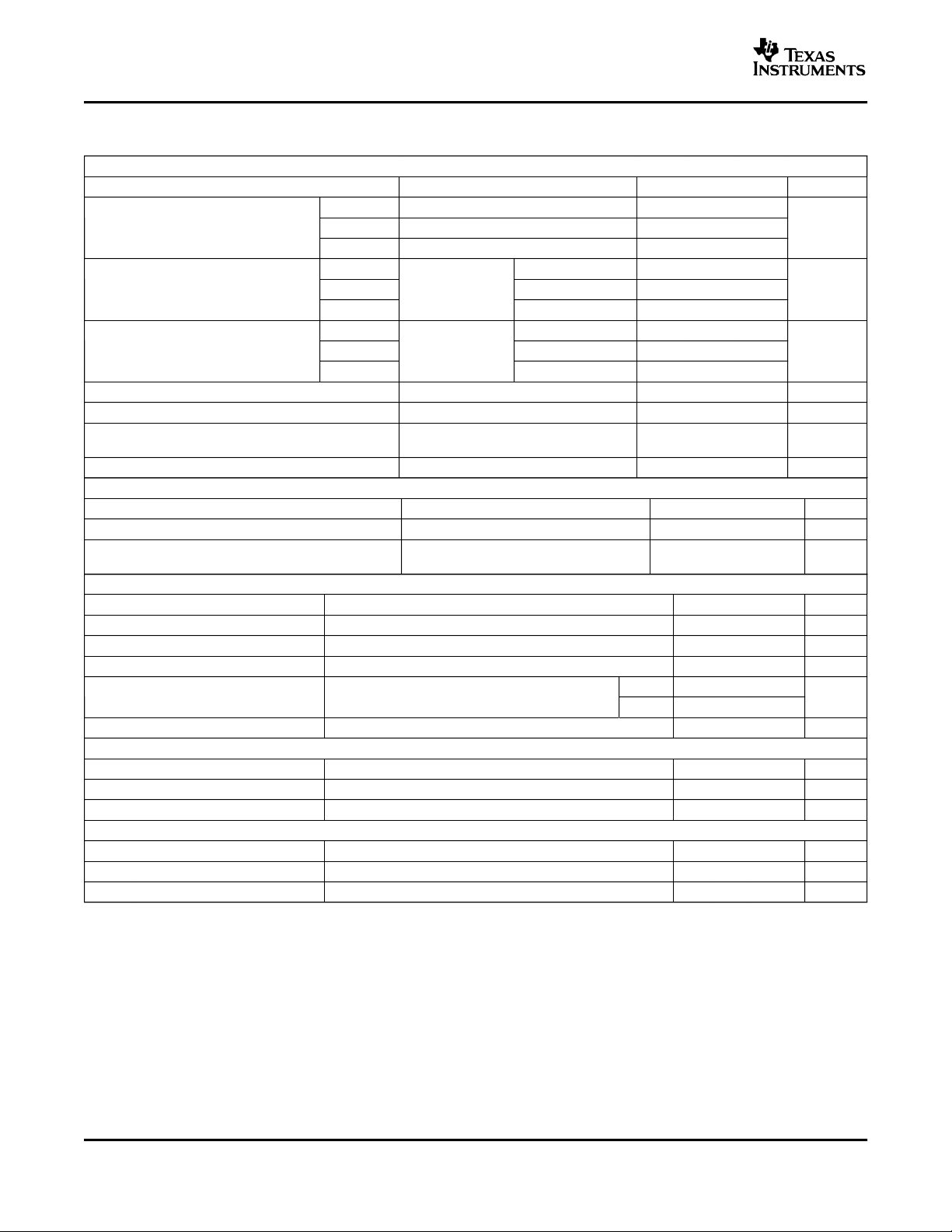
STATIC DAC SPECIFICATIONS
PARAMETER TEST CONDITIONS MIN TYP MAX UNIT
TLV5610 12
Resolution TLV5608 10 Bits
TLV5629 8
TLV5610 Code 40 to 4095 ±2 ±6
Integral nonlinearity (INL) TLV5608 V
TLV5629 Code 6 to 255 ±0.3 ±1
TLV5610 Code 40 to 4095 ±0.5 ±1
Differential nonlinearity (DNL) TLV5608 V
TLV5629 Code 6 to 255 ±0.1 ±1
E
ZS
E
ZS
E
G
Zero-scale error (offset error at zero scale) ±30 mV
TC Zero-scale-error temperature coefficient 30 µV/°C
Gain error ±0.6
EGTC Gain error temperature coefficient 10 ppm/°C
OUTPUT SPECIFICATIONS
PARAMETER TEST CONDITIONS MIN TYP MAX UNIT
V
O
Voltage output range RL= 10 kΩ 0 AV
Output load regulation accuracy RL= 2 kΩ vs 10 kΩ ±0.3
REFERENCE INPUT
PARAMETER TEST CONDITIONS MIN TYP MAX UNIT
V
Reference input voltage 0 AV
I
R
Reference input resistance 100 kΩ
i
C
Reference input capacitance 5 pF
i
Reference input bandwidth V
Reference feedthrough V
= 0.4 Vpp+ 2.048 V dc, Input code = 0x800 MHz
ref
= 2 Vppat 1 kHz + 2.048 V dc
ref
DIGITAL INPUT
I
High-level digital input current VI= V
IH
I
Low-level digital input current VI= 0 V -1 µA
IL
C
Input capacitance 8 pF
i
DD
DIGITAL OUTPUT
V
High-level digital output voltage RL= 10 kΩ 2.6 V
OH
V
Low-level digital output voltage RL= 10 kΩ 0.4 V
OL
Output voltage rise time RL= 10 kΩ, CL= 20 pF, Includes propogation delay 7 20 ns
(1) Reference feedthrough is measured at the DAC output with an input code = 0x000.
= 2 V, 4V Code 20 to 1023 ±0.5 ±2 LSB
ref
= 2 V, 4V Code 20 to 1023 ±0.1 ±1 LSB
ref
Fast 2.2
Slow 1.9
(1)
-84 dB
-0.4 V
DD
% of FS
voltage
DD
1 µA
% of FS
voltage
V
4
www.ti.com
TLV5608
TLV5610
TLV5629
SLAS268E – MAY 2000 – REVISED MARCH 2004
ELECTRICAL CHARACTERISTICS (CONTINUED)
over recommended operating free-air temperature range, supply voltages, and reference voltages (unless otherwise noted)
ANALOG OUTPUT DYNAMIC PERFORMANCE
PARAMETER TEST CONDITIONS MIN TYP MAX UNIT
Fast 1 3
t
s(FS)
t
s(CC)
Output settling time (full scale) RL= 10 kΩ, CL= 100 pF
Output settling time, code to code RL= 10 kΩ, CL= 100 pF
SR Slew rate RL= 10 kΩ, CL= 100 pF
Glitch energy See note
Channel crosstalk 10 kHz sine, 4 V
(4)
PP
(1) Settling time is the time for the output signal to remain within +0.5 LSB of the final measured value for a digital input code change of
0x80 to 0xFFF and 0xFFF to 0x080, respectively. Assured by design; not tested.
(2) Settling time is the time for the output signal to remain within +0.5 LSB of the final measured value for a digital input code change of one
count. The max time applies to code changes near zero scale or full scale. Assured by design; not tested.
(3) Slew rate determines the time it takes for a change of the DAC output from 10% to 90% full scale voltage.
(4) Code transition: TLV5610 - 0x7FF to 0x800, TLV5608 - 0x7FC to 0x800, TLV5629 - 0x7F0 to 0x800
(1)
Slow 3 7
Fast 0.5 1
(2)
Slow 1 2
Fast 4 10
(3)
Slow 1 3
4 nV-s
-90 dB
µs
µs
V/µs
TIMING REQUIREMENTS
DIGITAL INPUTS
MIN NOM MAX UNIT
t
su(FS-CK)
t
su(C16-FS)
t
su(FS-C17)
t
su(CK-FS)
t
wL(LDAC)
t
wH
t
wL
t
su(D)
t
h(D)
t
wH(FS)
t
wL(FS)
t
s
Setup time, FS low before next negative SCLK edge 8 ns
Setup time, 16
rising edge of FS. µC mode only
µC mode, setup time, FS high before 17
th
negative edge after FS low on which bit D0 is sampled before
th
positive SCLK. 10 ns
10 ns
DSP mode, setup time, SLCK low before FS low. 5 ns
LDAC duration low 10 ns
SCLK pulse duration high 16 ns
SCLK pulse duration low 16
Setup time, data ready before SCLK falling edge 8 ns
Hold time, data held valid after SCLK falling edge 5 ns
FS duration high 10 ns
FS duration low 10 ns
Settling time
See AC
specs
5

www.ti.com
1 2 3 4 16X X
X D15 D14 D13 D12 D1 X
SCLK
DIN
X D15 D14 D13 D12 D1 XDOUT
X
t
wH
t
wL
t
su(D)
t
h(D)
FS
FS
(DSP Mode)
t
wH(FS)
t
wL(FS)
t
su(FS - CK)
t
su(C16 - FS)
D0
D0
†
Previous input data
(µC mode)
† † † † † †
17
t
su(FS - C17)
t
su(CK - FS)
t
wL(LDAC)
LDAC
OUTx
t
s
±0.5 LSB
TLV5608
TLV5610
TLV5629
SLAS268E – MAY 2000 – REVISED MARCH 2004
PARAMETER MEASUREMENT INFORMATION
Figure 1. Serial Interface Timing
Figure 2. Output Timing
6

www.ti.com
TYPICAL CHARACTERISTICS
0
0.1
0.2
0.3
0.4
0.5
0.6
0.7
0.8
0.9
1
0
0.5
1
1.5
2
Fast
Slow
VDD = 5 V ,
V
ref
= 4 V ,
Zero Scale
− Output Voltage − V
Sinking Current − mA
V
O
0
0.1
0.2
0.3
0.4
0.5
0.6
0.7
0.8
0.9
1
0
0.5
1
1.5
2
Fast
Slow
VDD = 3 V ,
V
ref
= 2 V ,
Zero Scale
Sinking Current − mA
− Output Voltage − V
V
O
4.04
4.05
4.06
4.07
4.08
4.09
4.1
4.11
4.12
−4−3.5−3−2.5−2−1.5−1−0.50
Fast
Slow
− Output Voltage − V
V
O
Sourcing Current − mA
VDD = 5 V ,
V
ref
= 4 V ,
Full Scale
2.025
2.03
2.035
2.04
2.045
2.05
2.055
2.06
−4−3.5−3−2.5−2−1.5−1−0.5−0.05
Fast
Slow
− Output Voltage − V
V
O
Sourcing Current − mA
VDD = 3 V ,
V
ref
= 2 V ,
Full Scale
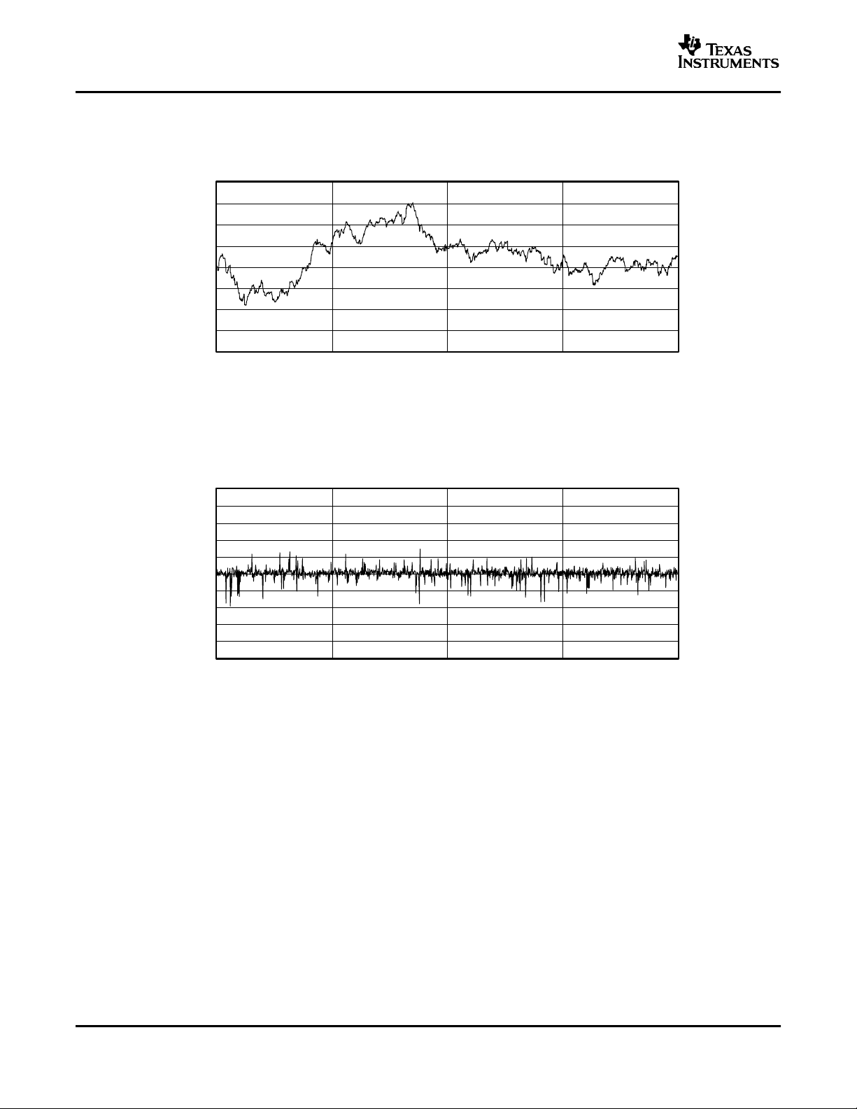
OUTPUT LOAD REGULATION OUTPUT LOAD REGULATION
TLV5608
TLV5610
TLV5629
SLAS268E – MAY 2000 – REVISED MARCH 2004
Figure 3. Figure 4.
OUTPUT LOAD REGULATION OUTPUT LOAD REGULATION
Figure 5. Figure 6.
7
www.ti.com
−4
−3
−2
−1
0
1
2
3
4
0 1024 2048 3072 4096
INL − Integral Nonlinearity − LSB
Code
−1.0
−0.8
−0.6
−0.4
−0.2
−0.0
0.2
0.4
0.6
0.8
1.0
0 1024 2048 3072 4096
DNL − Differential Nonlinearity − LSB
Code
TLV5608
TLV5610
TLV5629
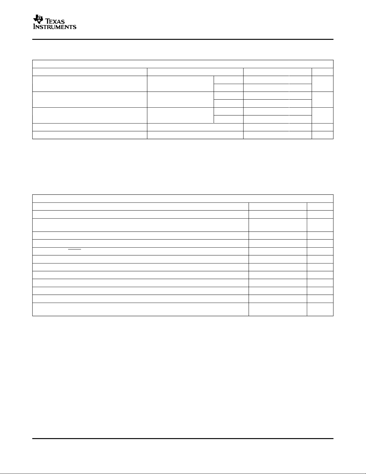
SLAS268E – MAY 2000 – REVISED MARCH 2004
TYPICAL CHARACTERISTICS (CONTINUED)
TLV5610
INTEGRAL NONLINEARITY
vs
CODE
Figure 7.
TLV5610
DIFFERENTIAL NONLINEARITY
vs
CODE
Figure 8.
8
www.ti.com
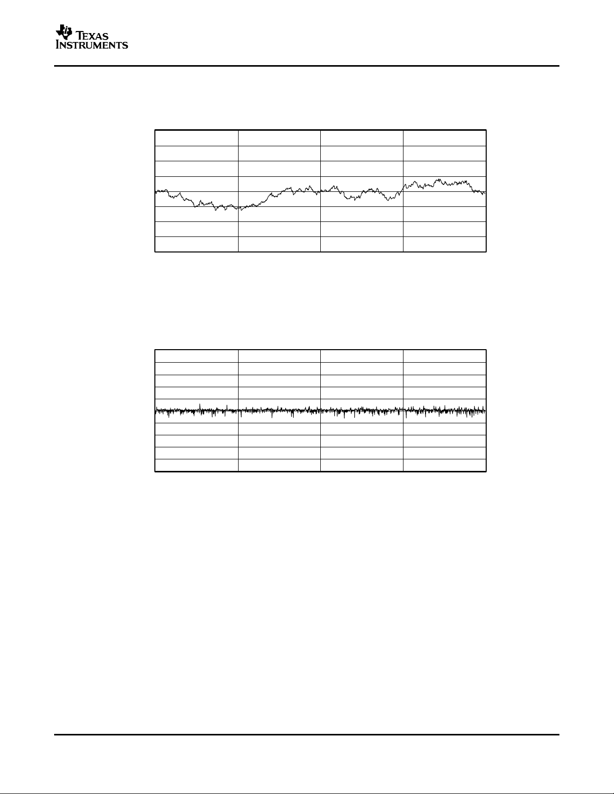
TYPICAL CHARACTERISTICS (CONTINUED)
−2.0
−1.5
−1.0
−0.5
0.0
0.5
1.0
1.5
2.0
0 256 512 768 1024
INL − Integral Nonlinearity − LSB
Code
−1.0
−0.8
−0.6
−0.4
−0.2
−0.0
0.2
0.4
0.6
0.8
1.0
0 256 512 768 1024
DNL − Differential Nonlinearity − LSB
Code
INTEGRAL NONLINEARITY
DIFFERENTIAL NONLINEARITY
TLV5608
TLV5610
TLV5629
SLAS268E – MAY 2000 – REVISED MARCH 2004
TLV5608
vs
CODE
Figure 9.
TLV5608
vs
CODE
Figure 10.
9
www.ti.com
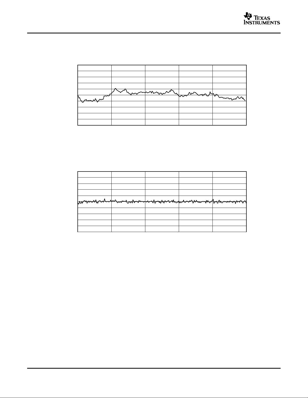
−0.5
−0.4
−0.3
−0.2
−0.1
0
0.1
0.2
0.3
0.4
0.5
0 50 100 150 200 250
INL − Integral Nonlinearity − LSB
Code
−0.5
−0.4
−0.3
−0.2
−0.1
0
0.1
0.2
0.3
0.4
0.5
0 50 100 150 200 250
DNL − Differential Nonlinearity − LSB
Code
TLV5608
TLV5610
TLV5629
SLAS268E – MAY 2000 – REVISED MARCH 2004
TYPICAL CHARACTERISTICS (CONTINUED)
TLV5629
INTEGRAL NONLINEARITY
vs
CODE
Figure 11.
TLV5629
DIFFERENTIAL NONLINEARITY
vs
CODE
Figure 12.
10

www.ti.com
REF
CODE
0x1000
[V]
SCLK
FS
DIN
SCLK
FS
F15F15XXE0 XE1E14E15D0D1D14D15X
DIN
F15F15XXE1 E0E14E15XD0D1D14D15X
DSP Mode:
µC Mode:
TLV5608
TLV5610
TLV5629
SLAS268E – MAY 2000 – REVISED MARCH 2004
APPLICATION INFORMATION
GENERAL FUNCTION
The TLV5610, TLV5608, and TLV5629 are 8-channel, 12-bit, single-supply DACs, based on a resistor string
architecture. They consist of a serial interface, a speed and power-down control logic, a reference input buffer, a
resistor string, and a rail-to-rail output buffer.
The output voltage (full scale determined by external reference) for each channel is given by:
where REF is the reference voltage and CODE is the digital input value. The input range is 0x000 to 0xFFF for
the TLV5610, 0x000 to 0xFFC for the TLV5608, and 0x000 to 0xFF0 for the TLV5629. A power-on-reset initially
puts the internal latches to a defined state (all bits zero).
SERIAL INTERFACE
A falling edge of FS starts shifting the data on DIN starting with the MSB to the internal register on the falling
edges of SCLK. After 16 bits have been transferred, the content of the shift register is moved to one of the DAC
holding registers, depending on the address bits within the data word. A logic 0 on the LDAC pin is required to
transfer the content of the DAC holding register to the DAC latch and to update the DAC outputs. LDAC is an
asynchronous input. It can be held low if a simultaneous update of all eight channels is not needed.
For daisy-chaining, DOUT provides the data sampled on DIN with a delay of 16 clock cycles.
(1)
Figure 13. Data Sampled on DIN
Difference between DSP mode (MODE = N.C. or 0) and µC (MODE = 1) mode:
• In µC mode, FS needs to be held low until all 16 data bits have been transferred. If FS is driven high before
the 16th falling clock edge, the data transfer is cancelled. The DAC is updated after a rising edge on FS.
• In DSP mode, FS needs to stay low for 20 ns and can go high before the 16th falling clock edge.
• In DSP mode there needs to be one falling SCLK edge before FS goes low to start the write (DIN) cycle.
This extra falling SCLK edge has to happen at least 5 ns before FS goes low, t
su(CK-FS)
• In µC mode, the extra falling SCLK edge is not necessary. However, if it does happen, the extra negative
SCLK edge is not allowed to occur within 10 ns after FS goes HIGH to finish the WRITE cycle (t
≥ 5 ns.
su(FS-C17)
).
11
www.ti.com
f
sclkmax
1
t
whmin
t
wlmin
30 MHz
f
updatemax
1
16t
whmin
t
wlmin
1.95 MHz
TLV5608
TLV5610
TLV5629
SLAS268E – MAY 2000 – REVISED MARCH 2004
APPLICATION INFORMATION (continued)
SERIAL CLOCK FREQUENCY AND UPDATE RATE
The maximum serial clock frequency is given by:
The maximum update rate is:
Note, that the maximum update rate is just a theoretical value for the serial interface, as the settling time of the
DAC has to be considered also.
DATA FORMAT
The 16-bit data word consists of two parts:
• Address bits (D150D12)
• Data bits (D110D0)
D15 D14 D13 D12 D11 D10 D9 D8 D7 D6 D5 D4 D3 D2 D1 D0
A3 A2 A1 A0 DATA
(2)
(3)
Register Map
A3 A2 A1 A0 FUNCTION
0 0 0 0 DAC A
0 0 0 1 DAC B
0 0 1 0 DAC C
0 0 1 1 DAC D
0 1 0 0 DAC E
0 1 0 1 DAC F
0 1 1 0 DAC G
0 1 1 1 DAC H
1 0 0 0 CTRL0
1 0 0 1 CTRL1
1 0 1 0 Preset
1 0 1 1 Reserved
1 1 0 0 DAC A and B
1 1 0 1 DAC C and D
1 1 1 0 DAC E and F
1 1 1 1 DAC G and H
DAC A-H AND TWO-CHANNEL REGISTERS
Writing to DAC A-H sets the output voltage of channel A-H. It is possible to automatically generate the
complement of one channel by writing to one of the four two-channel registers (DAC A and B etc.).
The TLV5610 decodes all 12 data bits. The TLV5608 decodes D11 to D2 (D1 and D0 are ignored). The TLV5629
decodes D11 to D4 (D3 to D0 are ignored).
12
www.ti.com
TLV5608
TLV5610
TLV5629
SLAS268E – MAY 2000 – REVISED MARCH 2004
PRESET
The outputs of all DAC channels can be driven to a predefined value stored in the Preset register by driving the
PRE input low. The PRE input is asynchronous to the clock.
CTRL0
D11 D10 D9 D8 D7 D6 D5 D4 D3 D2 D1 D0
X X X X X X X PD DO X X IM
PD : Full device power down 0 = normal 1 = power down
DO : Digital output enable 0 = disable 1 = enable
IM : Input mode 0 = straight binary 1 = twos complement
X : Reserved
If DOUT is enabled, the data input on DIN is output on DOUT with a 16-cycle delay. That makes it possible to
daisy-chain multiple DACs on one serial bus.
CTRL1
D11 D10 D9 D8 D7 D6 D5 D4 D3 D2 D1 D0
X X X X P
GH
P
P
EF
CD
P
AB
S
GH
S
EF
S
CD
S
AB
P
S
XY
XY
: Power down DAC
: Speed DAC
0 = normal 1 = power down
XY
XY
0 = slow 1 = fast
XY : DAC pair AB, CD, EF, or GH
In power-down mode, the amplifiers of the selected DAC pair within the device are disabled and the total power
consumption of the device is significantly reduced. Power-down mode of a specific DAC pair can be selected by
setting the PXY bit within the data word to 1.
There are two settling time modes: fast and slow. Fast mode of a DAC pair is selected by setting S
slow mode is selected by setting S
to 0.
XY
to 1 and
XY
13


MECHANICAL DATA
MTSS001C – JANUARY 1995 – REVISED FEBRUARY 1999
PW (R-PDSO-G**) PLASTIC SMALL-OUTLINE PACKAGE
14 PINS SHOWN
0,65
1,20 MAX
14
0,30
0,19
8
4,50
4,30
PINS **
7
Seating Plane
0,15
0,05
8
1
A
DIM
14
0,10
6,60
6,20
M
0,10
0,15 NOM
0°–8°
2016
Gage Plane
24
0,25
0,75
0,50
28
A MAX
A MIN
NOTES: A. All linear dimensions are in millimeters.
B. This drawing is subject to change without notice.
C. Body dimensions do not include mold flash or protrusion not to exceed 0,15.
D. Falls within JEDEC MO-153
3,10
2,90
5,10
4,90
5,10
4,90
6,60
6,40
7,90
7,70
9,80
9,60
4040064/F 01/97
POST OFFICE BOX 655303 • DALLAS, TEXAS 75265

IMPORTANT NOTICE
Texas Instruments Incorporated and its subsidiaries (TI) reserve the right to make corrections, modifications,
enhancements, improvements, and other changes to its products and services at any time and to discontinue
any product or service without notice. Customers should obtain the latest relevant information before placing
orders and should verify that such information is current and complete. All products are sold subject to TI’s terms
and conditions of sale supplied at the time of order acknowledgment.
TI warrants performance of its hardware products to the specifications applicable at the time of sale in
accordance with TI’s standard warranty. Testing and other quality control techniques are used to the extent TI
deems necessary to support this warranty . Except where mandated by government requirements, testing of all
parameters of each product is not necessarily performed.
TI assumes no liability for applications assistance or customer product design. Customers are responsible for
their products and applications using TI components. To minimize the risks associated with customer products
and applications, customers should provide adequate design and operating safeguards.
TI does not warrant or represent that any license, either express or implied, is granted under any TI patent right,
copyright, mask work right, or other TI intellectual property right relating to any combination, machine, or process
in which TI products or services are used. Information published by TI regarding third-party products or services
does not constitute a license from TI to use such products or services or a warranty or endorsement thereof.
Use of such information may require a license from a third party under the patents or other intellectual property
of the third party, or a license from TI under the patents or other intellectual property of TI.
Reproduction of information in TI data books or data sheets is permissible only if reproduction is without
alteration and is accompanied by all associated warranties, conditions, limitations, and notices. Reproduction
of this information with alteration is an unfair and deceptive business practice. TI is not responsible or liable for
such altered documentation.
Resale of TI products or services with statements different from or beyond the parameters stated by TI for that
product or service voids all express and any implied warranties for the associated TI product or service and
is an unfair and deceptive business practice. TI is not responsible or liable for any such statements.
Following are URLs where you can obtain information on other Texas Instruments products and application
solutions:
Products Applications
Amplifiers amplifier.ti.com Audio www.ti.com/audio
Data Converters dataconverter.ti.com Automotive www.ti.com/automotive
DSP dsp.ti.com Broadband www.ti.com/broadband
Interface interface.ti.com Digital Control www.ti.com/digitalcontrol
Logic logic.ti.com Military www.ti.com/military
Power Mgmt power.ti.com Optical Networking www.ti.com/opticalnetwork
Microcontrollers microcontroller.ti.com Security www.ti.com/security
Telephony www.ti.com/telephony
Video & Imaging www.ti.com/video
Wireless www.ti.com/wireless
Mailing Address: Texas Instruments
Post Office Box 655303 Dallas, Texas 75265
Copyright 2004, Texas Instruments Incorporated
 Loading...