

Page 1
2.7-V TO 5.5-V 10-BIT 3-µS QUADRUPLE DIGITAL-TO-ANALOG CONVERTERS
D
Four 10-Bit D/A Converters
D
Programmable Settling Time
of 3 µs or 9 µs Typ
D
TMS320, (Q)SPI, and Microwire
Compatible Serial Interface
D
Internal Power-On Reset
D
Low Power Consumption:
5.5 mW, Slow Mode – 5-V Supply
3.3 mW, Slow Mode – 3-V Supply
D
Reference Input Buffers
D
Voltage Output Range ...2× the Reference
Input Voltage
D
Monotonic Over Temperature
D
Dual 2.7-V to 5.5-V Supply (Separate Digital
and Analog Supplies)
description
The TL V5604 is a quadruple 10-bit voltage output
digital-to-analog converter (DAC) with a flexible
4-wire serial interface. The 4-wire serial interface
allows glueless interface to TMS320, SPI, QSPI,
and Microwire serial ports. The TLV5604 is
programmed with a 16-bit serial word comprised
of a DAC address, individual DAC control bits, and
a 10-bit DAC value.
SLAS176B – DECEMBER 1997 – REVISED JUL Y 2002
WITH POWER DOWN
D
Hardware Power Down (10 nA)
D
Software Power Down (10 nA)
D
Simultaneous Update
applications
D
Battery Powered Test Instruments
D
Digital Offset and Gain Adjustment
D
Industrial Process Controls
D
Machine and Motion Control Devices
D
Communications
D
Arbitrary Waveform Generation
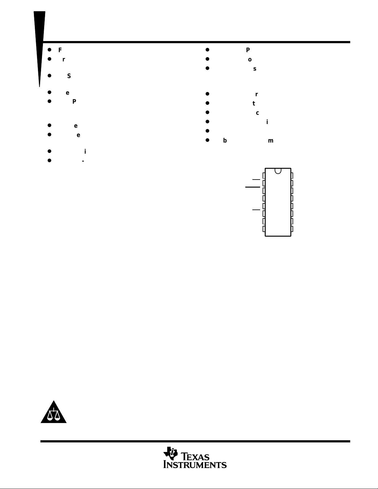
D OR PW PACKAGE
(TOP VIEW)
DV
DD
PD
LDAC
DIN
SCLK
CS
FS
DGND
16
1
15
2
14
3
13
4
12
5
11
6
10
7
8
9
AV
DD
REFINAB
OUTA
OUTB
OUTC
OUTD
REFINCD
AGND
TLV5604
The device has provision for two supplies: one digital supply for the serial interface (via pins DV
and one for the DACs, reference buffers and output buffers (via pins AV
and AGND). Each supply is
DD
and DGND),
DD
independent of the other, and can be any value between 2.7 V and 5.5 V. The dual supplies allow a typical
application where the DAC will be controlled via a microprocessor operating on a 3-V supply (also used on pins
DV
and DGND), with the DACs operating on a 5-V supply . Of course, the digital and analog supplies can be
DD
tied together.
The resistor string output voltage is buffered by a x2 gain rail-to-rail output buffer . The buffer features a Class AB
output stage to improve stability and reduce settling time. A rail-to-rail output stage and a power-down mode
makes it ideal for single voltage, battery based applications. The settling time of the DAC is programmable to
allow the designer to optimize speed versus power dissipation. The settling time is chosen by the control bits
within the 16-bit serial input string. A high-impedance buffer is integrated on the REFINAB and REFINCD
terminals to reduce the need for a low source impedance drive to the terminal. REFINAB and REFINCD allow
DACs A and B to have a different reference voltage then DACs C and D.
The device, implemented with a CMOS process, is available in 16-terminal SOIC and TSSOP packages. The
TL V5604C is characterized for operation from 0°C to 70°C. The TLV5604I is characterized for operation from
–40°C to 85°C.
Please be aware that an important notice concerning availability, standard warranty, and use in critical applications of
Texas Instruments semiconductor products and disclaimers thereto appears at the end of this data sheet.
SPI and QSPI are trademarks of Motorola, Inc.
Microwire is a trademark of National Semiconductor Corporation.
PRODUCTION DATA information is current as of publication date.
Products conform to specifications per the terms of Texas Instruments
standard warranty. Production processing does not necessarily include
testing of all parameters.
Copyright 2002, Texas Instruments Incorporated
POST OFFICE BOX 655303 • DALLAS, TEXAS 75265
1
Page 2
TLV5604
2.7-V TO 5.5-V 10-BIT 3-µS QUADRUPLE DIGITAL-TO-ANALOG CONVERTERS
WITH POWER DOWN
SLAS176B – DECEMBER 1997 – REVISED JULY 2002
AVAILABLE OPTIONS
PACKAGE
functional block diagram
T
A
0°C to 70°C TLV5604CD TLV5604CPW
–40°C to 85°C TLV5604ID TLV5604IPW
SOIC
(D)
TSSOP
(PW)
REFINAB
SCLK
AV
DD
15 16 1
DAC A
+
_
10-Bit
DAC
Latch
2-Bit
Control
Data
Latch
DAC B
DIN
FS
CS
4
7
5
6
Power-On
Reset
Serial
Input
Register
2
DAC
Select/
Control
Logic
14
14-Bit
Data
and
Control
Register
10
2
DV
DD
10
2
Power Down/
Speed Control
x2
13
14
OUTA
OUTB
REFINCD
2
9
AGND
8
DGND
32
LDAC
POST OFFICE BOX 655303 • DALLAS, TEXAS 75265
DAC C
DAC D
PD
12
11
OUTC
OUTD
Page 3

TLV5604
2.7-V TO 5.5-V 10-BIT 3-µS QUADRUPLE DIGITAL-TO-ANALOG CONVERTERS
WITH POWER DOWN
SLAS176B – DECEMBER 1997 – REVISED JULY 2002
3
Page 4
TLV5604
Supply voltage, AV
DV
V
High-level digital input voltage, V
V
Low-level digital input voltage, V
V
Reference voltage, V
to REFINAB, REFINCD terminal
V
Operating free-air temperature
°C
PSRR
Power supply rejection ratio
See Notes 8 and 9
dB
2.7-V TO 5.5-V 10-BIT 3-µS QUADRUPLE DIGITAL-TO-ANALOG CONVERTERS
WITH POWER DOWN
SLAS176B – DECEMBER 1997 – REVISED JULY 2002
recommended operating conditions
MIN NOM MAX UNIT
pp
Load resistance, R
Load capacitance, C
Serial clock rate, SCLK 20 MHz
p
NOTE 1: Voltages greater than AVDD/2 will cause output saturation for large DAC codes.
p
DD
p
L
L
ref
,
DD
IH
IL
p
electrical characteristics over recommended operating free-air temperature range
(unless otherwise noted)
5-V supply 4.5 5 5.5
3-V supply 2.7 3 3.3
DVDD = 2.7 V 2
DVDD = 5.5 V 2.4
DVDD = 2.7 V 0.6
DVDD = 5.5 V 1
5-V supply (see Note 1) 0 2.048 AVDD–1.5
3-V supply (see Note 1) 0 1.024 AVDD–1.5
2 10 kΩ
100 pF
TLV5604C 0 70
TLV5604I –40 85
°
static DAC specifications
PARAMETER TEST CONDITIONS MIN TYP MAX UNIT
Resolution 10 bits
Integral nonlinearity (INL), end point adjusted See Note 2 ±1 LSB
Differential nonlinearity (DNL) See Note 3 ±0.1 ±1 LSB
E
ZS
E
G
NOTES: 2. The relative accuracy or integral nonlinearity (INL) sometimes referred to as linearity error , is the maximum deviation of the output
Zero scale error (offset error at zero scale) See Note 4 ±12 mV
Zero scale error temperature coefficient See Note 5 10 ppm/°C
min
).
%of FS
voltage
Gain error See Note 6 ±0.6
Gain error temperature coefficient See Note 7 10 ppm/°C
pp
from the line between zero and full scale excluding the effects of zero code and full-scale errors.
3. The differential nonlinearity (DNL) sometimes referred to as differential error, is the difference between the measured and ideal
1 LSB amplitude change of any two adjacent codes. Monotonic means the output voltage changes in the same direction (or remains
constant) as a change in the digital input code.
4. Zero-scale error is the deviation from zero voltage output when the digital input code is zero.
5. Zero-scale-error temperature coefficient is given by: EZS TC = [EZS (T
6. Gain error is the deviation from the ideal output (2V
7. Gain temperature coefficient is given by: EG TC = [EG(T
8. Zero-scale-error rejection ratio (EZS–RR) is measured by varying the AVDD from 5 ±0.5 V and 3 ±0.3 V dc, and measuring the
proportion of this signal imposed on the zero-code output voltage.
9. Gain-error rejection ratio (EG-RR) is measured by varying the AVDD from 5 ±0.5 V and 3 ±0.3 V dc and measuring the proportion
of this signal imposed on the full-scale output voltage after subtracting the zero scale change.
Zero scale gain
Gain
) – EZS (T
– 1 LSB) with an output load of 10 kΩ excluding the effects of the zero-error .
ref
max
) – EG (T
max
min
)]/V
× 106/(T
ref
min
)]/V
max
ref
– T
× 106/(T
).
min
–80
–80
max
– T
4
POST OFFICE BOX 655303 • DALLAS, TEXAS 75265
Page 5
Reference input bandwidth
REFIN
V
1.024 V dc
MHz
5-V supply
load, Clock running
mA
IDDPower supply current
3-V supply
load, Clock running
mA
2.7-V TO 5.5-V 10-BIT 3-µS QUADRUPLE DIGITAL-TO-ANALOG CONVERTERS
WITH POWER DOWN
SLAS176B – DECEMBER 1997 – REVISED JULY 2002
electrical characteristics over recommended operating free-air temperature range
(unless otherwise noted) (continued)
individual DAC output specifications
PARAMETER TEST CONDITIONS MIN TYP MAX UNIT
V
O
reference input (REFINAB, REFINCD)
V
I
R
I
C
I
NOTES: 10. Reference input voltages greater than VDD/2 will cause output saturation for large DAC codes.
Voltage output RL = 10 kΩ 0 AVDD–0.4 V
Output load regulation accuracy RL = 2 kΩ vs 10 kΩ 0.1 0.25
PARAMETER TEST CONDITIONS MIN TYP MAX UNIT
Input voltage range See Note 10 0 AVDD–1.5 V
Input resistance 10 MΩ
Input capacitance 5 pF
Reference feed through
p
11. Reference feedthrough is measured at the DAC output with an input code = 000 hex and a V
input = 1.024 Vdc + 1 Vpp at 1 kHz.
REFIN = 1 Vpp at 1 kHz + 1.024 V dc
(see Note 11)
= 0.2
pp
+
–75 dB
Slow 0.5
Fast 1
ref(REFINAB or REFINCD)
TLV5604
% of FS
voltage
digital inputs (D0–D11, CS, WEB, LDAC, PD)
PARAMETER TEST CONDITIONS MIN TYP MAX UNIT
I
IH
I
IL
C
I
High-level digital input current VI = DV
Low-level digital input current VI = 0 V ±1 µA
Input capacitance 3 pF
power supply
PARAMETER TEST CONDITIONS MIN TYP MAX UNIT
pp
Power down supply current,
See Figure 12
pp
pp
, No
, No
DD
Slow 1.4 2.2
Fast 3.5 5.5
Slow 1 1.5
Fast 3 4.5
±1 µA
10 nA
POST OFFICE BOX 655303 • DALLAS, TEXAS 75265
5
Page 6
TLV5604
SR
Output slew rate
V
10% to 90%
tsOutput settling time
,
L
,
s
t
Output settling time, code to code
,
L
,
s
S,
f
s
400 KSPS
C
L
100 pF
R
L
2.7-V TO 5.5-V 10-BIT 3-µS QUADRUPLE DIGITAL-TO-ANALOG CONVERTERS
WITH POWER DOWN
SLAS176B – DECEMBER 1997 – REVISED JULY 2002
electrical characteristics over recommended operating free-air temperature range
(unless otherwise noted) (continued)
analog output dynamic performance
PARAMETER TEST CONDITIONS MIN TYP MAX UNIT
p
p
s(c)
SNR Signal-to-noise ratio
S/(N+D) Signal to noise + distortion
THD Total harmonic Distortion
SFDR Spurious free dynamic range
NOTES: 12. Settling time is the time for the output signal to remain within ± 0.5LSB of the final measured value for a digital input code change
p
Glitch energy Code transition from 7FF to 800 10 nV-sec
of 020 hex to 3FF hex or 3FF hex to 020 hex.
13. Settling time is the time for the output signal to remain within ± 0.5LSB of the final measured value for a digital input code change
of one count, 1FF hex to 200 hex.
14. Limits are ensured by design and characterization, but are not production tested.
CL = 100 pF, RL = 10 kΩ,
=
O
V
= 2.048 V, 1024 V
ref
To ± 0.5 LSB, C
RL = 10 kΩ, See Notes 12 and 14
To ± 0.5 LSB, C
RL = 10 kΩ, See Note 13
Sinewave generated by DAC,
Reference voltage = 1.024 at 3 V and 2.048 at 5 V ,
= 400 KSP
=
f
f
= 1.1 kHz sinewave,
OUT
=
BW = 20 kHz
p
,
,
,
= 100 pF,
= 100 pF,
= 10 kΩ,
Fast 5 V/µs
Slow 1 V/µs
Fast 2.5 4
Slow 8.5 18
Fast 1
Slow 2
68
65
–68
70
µ
µ
dB
6
POST OFFICE BOX 655303 • DALLAS, TEXAS 75265
Page 7

TLV5604
2.7-V TO 5.5-V 10-BIT 3-µS QUADRUPLE DIGITAL-TO-ANALOG CONVERTERS
WITH POWER DOWN
SLAS176B – DECEMBER 1997 – REVISED JULY 2002
7
Page 8
TLV5604
2.7-V TO 5.5-V 10-BIT 3-µS QUADRUPLE DIGITAL-TO-ANALOG CONVERTERS
WITH POWER DOWN
SLAS176B – DECEMBER 1997 – REVISED JULY 2002
TYPICAL CHARACTERISTICS
LOAD REGULATION
0.35
VDD = 5 V,
V
= 2 V,
0.30
0.25
0.20
0.15
– Output Voltage – V
O
0.10
V
0.05
REF
VO = Full Scale
5 V Slow Mode, Sink
5 V Fast Mode, Sink
0
0 0.02 0.04 0.1 0.2 0.4 1
Load Current – mA
Figure 2
LOAD REGULATION
4.002
0.8
24
LOAD REGULATION
0.20
VDD = 3 V,
0.18
V
= 1 V,
REF
VO = Full Scale
0.16
0.14
0.12
0.10
0.08
– Output Voltage – V
0.06
O
V
0.04
0.02
0
0 0.01 0.02 0.05 0.1 0.2 0.5
3 V Fast Mode, Sink
Load Current – mA
Figure 3
3 V Slow Mode, Sink
0.8
12
3.998
3.996
3.994
3.992
– Output Voltage – V
3.988
3.986
3.984
4.00
3.99
Load Current
Figure 4
8
POST OFFICE BOX 655303 • DALLAS, TEXAS 75265
Page 9
TLV5604
2.7-V TO 5.5-V 10-BIT 3-µS QUADRUPLE DIGITAL-TO-ANALOG CONVERTERS
WITH POWER DOWN
SLAS176B – DECEMBER 1997 – REVISED JULY 2002
TYPICAL CHARACTERISTICS
SUPPLY CURRENT
TEMPERATURE
4
VDD = 3 V,
V
= 1.024 V,
REF
3.5
VO = Full Scale
3
2.5
2
– Supply Current – mA
1.5
DD
I
1
0.5
–40 –20 0 20 40 60
T – Temperature – °C
Figure 6
vs
Fast Mode
Slow Mode
80 100
– Supply Current – mA
DD
I
3.5
2.5
1.5
0.5
SUPPLY CURRENT
vs
TEMPERATURE
4
Fast Mode
3
2
Slow Mode
1
T – Temperature – °C
Figure 7
POST OFFICE BOX 655303 • DALLAS, TEXAS 75265
9
Page 10
TLV5604
2.7-V TO 5.5-V 10-BIT 3-µS QUADRUPLE DIGITAL-TO-ANALOG CONVERTERS
WITH POWER DOWN
SLAS176B – DECEMBER 1997 – REVISED JULY 2002
TYPICAL CHARACTERISTICS
TOTAL HARMONIC DISTORTION AND NOISE
vs
FREQUENCY
0
V
= 1 V dc + 1 V p/p Sinewave,
ref
Output Full Scale
Fast Mode
0 5 10 20
f – Frequency – kHz
30 50 100
THD – Total Harmonic Distortion And Noise – dB
–10
–20
–30
––40
–50
–60
–70
–80
Figure 10
(WHEN ENTERING POWER-DOWN MODE)
4000
–10
–20
–30
––40
–50
–60
–70
THD – Total Harmonic Distortion And Noise – dB
–80
SUPPLY CURRENT
vs
TIME
TOTAL HARMONIC DISTORTION AND NOISE
vs
FREQUENCY
0
V
= 1 V dc + 1 V p/p Sinewave,
ref
Output Full Scale
Slow Mode
0 5 10 20
f – Frequency – kHz
30 50 100
Figure 11
3500
3000
Aµ
2500
2000
1500
– Supply Current –
DD
1000
I
500
0
0 200 400 600
800 1000
t – Time – ns
Figure 12
10
POST OFFICE BOX 655303 • DALLAS, TEXAS 75265
Page 11

TLV5604
2.7-V TO 5.5-V 10-BIT 3-µS QUADRUPLE DIGITAL-TO-ANALOG CONVERTERS
WITH POWER DOWN
SLAS176B – DECEMBER 1997 – REVISED JULY 2002
TYPICAL CHARACTERISTICS
INL – Integral Nonlinearity – LSB
0.2
0
–0.2
–0.4
–0.6
0 64 128 192 256 320 384
INTEGRAL NONLINEARITY
VDD = 5 V, Vref = 2 V,
CLK = 1 MHz
448 512 704
Digital Code
576 640 768 832
Figure 13
896 960
1024
POST OFFICE BOX 655303 • DALLAS, TEXAS 75265
11
Page 12

TLV5604
2.7-V TO 5.5-V 10-BIT 3-µS QUADRUPLE DIGITAL-TO-ANALOG CONVERTERS
WITH POWER DOWN
SLAS176B – DECEMBER 1997 – REVISED JULY 2002
APPLICATION INFORMATION
general function
The TL V5604 is a 10-bit single supply DAC based on a resistor string architecture. The device consists of a serial
interface, speed and power-down control logic, a reference input buffer , a resistor string, and a rail-to-rail output
buffer.
The output voltage (full scale determined by external reference) is given by:
2REF
CODE
Where REF is the reference voltage and CODE is the digital input value within the range of 0
[V]
n
2
to 2n–1, where
10
n=10 (bits). The 16-bit data word, consisting of control bits and the new DAC value, is illustrated in the data
format section. A power-on reset initially resets the internal latches to a defined state (all bits zero).
serial interface
Explanation of data transfer: First, the device has to be enabled with CS set to low . Then, a falling edge of FS
starts shifting the data bit-per-bit (starting with the MSB) to the internal register on the falling edges of SCLK.
After 16 bits have been transferred or FS rises, the content of the shift register is moved to the DAC latch, which
updates the voltage output to the new level.
The serial interface of the TLV5604 can be used in two basic modes:
D
Four wire (with chip select)
D
Three wire (without chip select)
Using chip select (four wire mode), it is possible to have more than one device connected to the serial port of
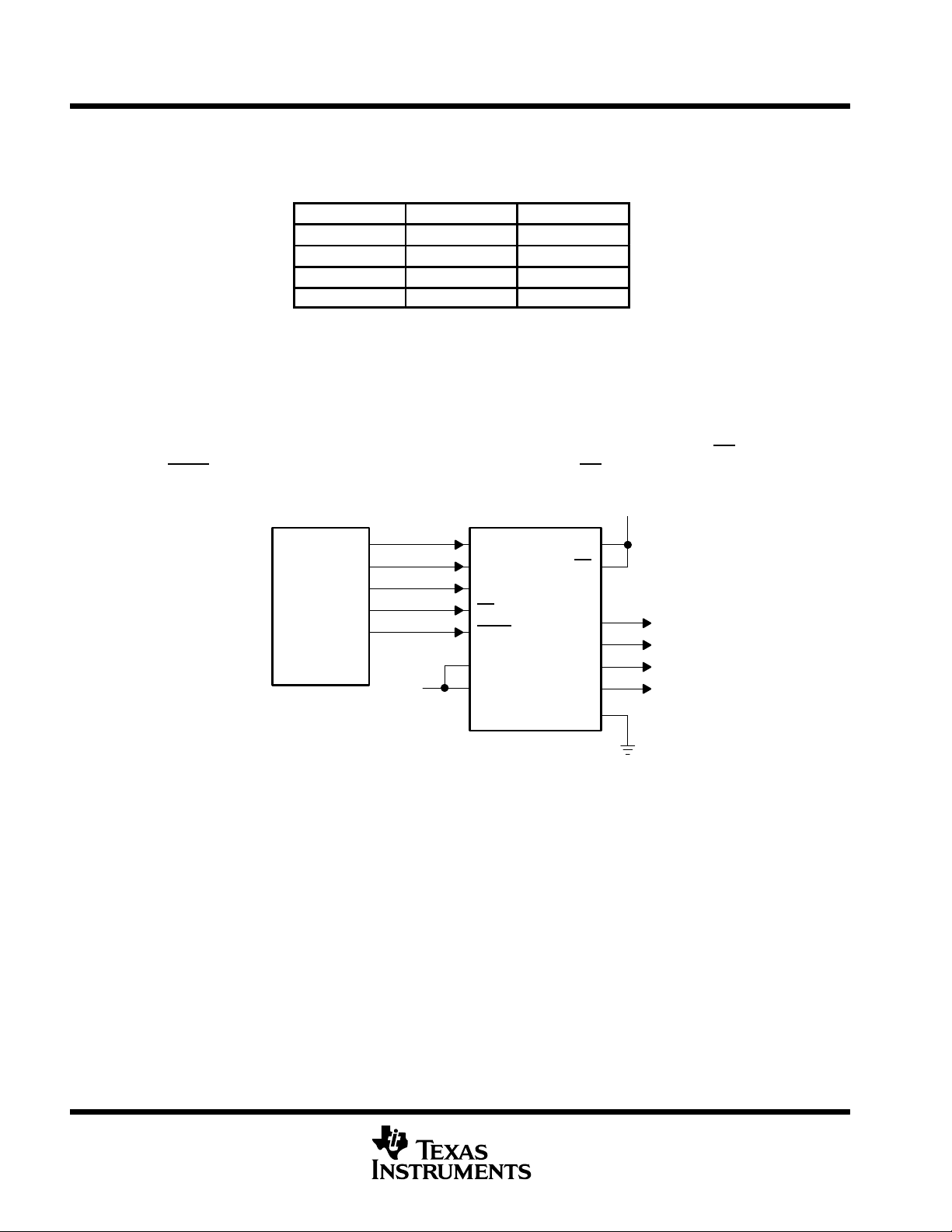
the data source (DSP or microcontroller). The interface is compatible with the TMS320 family . Figure 15 shows
an example with two TLV5604s connected directly to a TMS320 DSP.
TLV5604
CS
FS DIN SCLK
TLV5604
CS
FS DIN SCLK
12
TMS320
DSP
XF0
XF1
FSX
DX
CLKX
Figure 15. TMS320 Interface
POST OFFICE BOX 655303 • DALLAS, TEXAS 75265
Page 13

2.7-V TO 5.5-V 10-BIT 3-µS QUADRUPLE DIGITAL-TO-ANALOG CONVERTERS
WITH POWER DOWN
SLAS176B – DECEMBER 1997 – REVISED JULY 2002
APPLICATION INFORMATION
serial interface (continued)
If there is no need to have more than one device on the serial bus, then CS can be tied low. Figure 16 shows
an example of how to connect the TLV5604 to a TMS320, SPI, or Microwire port using only three pins.
TLV5604
TMS320
DSP
FSX
DX
CLKX
TLV5604
FS
DIN
SCLK
CS
SPI
SS
MOSI
SCLK
TLV5604
FS
DIN
SCLK
CS
Microwire
I/O
SO
SK
TLV5604
FS
DIN
SCLK
CS
Figure 16. Three-Wire Interface
Notes on SPI and Microwire: Before the controller starts the data transfer, the software has to generate a falling
edge on the I/O pin connected to FS. If the word width is 8 bits (SPI and Microwire), two write operations must
be performed to program the TLV5604. After the write operation(s), the DAC output is updated automatically
on the next positive clock edge following the sixteenth falling clock edge.
serial clock frequency and update rate
The maximum serial clock frequency is given by:
f
SCLKmax
+
t
wH(min)
The maximum update rate is:
f
UPDATEmax
+
16
ǒ
1
)
t
wL(min)
t
wH(min)
1
)
+
20 MHz
t
wL(min)
+
Ǔ
1.25 MHz
Note that the maximum update rate is a theoretical value for the serial interface since the settling time of the
TLV5604 has to be considered also.
data format
The 16-bit data word for the TLV5604 consists of two parts:
D
Control bits (D15 . . . D12)
D
New DAC value (D11 ...D0)
D15 D14 D13 D12 D11 D10 D9 D8 D7 D6 D5 D4 D3 D2 D1 D0
A1 A0 PWR SPD New DAC value (10 bits) X X
X: don’t care
SPD: Speed control bit. 1 → fast mode 0 → slow mode
PWR: Power control bit. 1 → power down 0 → normal operation
POST OFFICE BOX 655303 • DALLAS, TEXAS 75265
13
Page 14
TLV5604
2.7-V TO 5.5-V 10-BIT 3-µS QUADRUPLE DIGITAL-TO-ANALOG CONVERTERS
WITH POWER DOWN
SLAS176B – DECEMBER 1997 – REVISED JULY 2002
APPLICATION INFORMATION
In power down mode, all amplifiers within the TLV5604 are disabled. A particular DAC (A, B, C, D) of the
TLV5604 is selected by A1 and A0 within the input word.
A1 A0 DAC
0 0 A
0 1 B
1 0 C
1 1 D
TLV5604 interfaced to TMS320C203 DSP
Hardware interfacing
Figure 17 shows an example of how to connect the TLV5604 to a TMS320C203 DSP. The serial port is
configured in burst mode, with FSX generated by the TMS320C203 to provide the Frame Sync (FS) input to
the TLV5604. Data is transmitted on the DX line, with the serial clock input on the CLKX line. The
general-purpose input/output port bits IO0 and IO1 are used to generate the Chip Select (CS
Update (LDAC
) inputs to the TL V5604. The active low Power Down (PD) is pulled high all the time to ensure
the DACs are enabled.
TMS320C203
TLV5604
) and DAC Latch
DX
CLKX
FSX
I/O 0
I/O 1
REF
SDIN
SCLK
FS
CS
LDAC
REFINAB
REFINCD
V
DD
PD
VOUTA
VOUTB
VOUTC
VOUTD
V
SS
Figure 17. TL V5604 Interfaced with TMS320C203
Software
The application example generates a differential in-phase (sine) signal between the VOUT A and VOUTB pins,
and it is quadrature (cosine) signal as the differential signal between VOUTC and VOUTD.
The on-chip timer is used to generate interrupts at a fixed frequency . The related interrupt service routine pulses
LDAC low to update all 4 DACs simultaneously, then fetches and writes the next sample to all 4 DACs. The
samples are stored in a look-up table, which describes two full periods of a sine wave.
The synchronous serial port of the DSP is used in burst mode. In this mode, the processor generates an FS
pulse preceding the MSB of every data word. If multiple, contiguous words are transmitted, a violation of the
tsu(C16-FS) timing requirement will occur. T o avoid this, the program waits until the transmission of the previous
word has been completed.
14
POST OFFICE BOX 655303 • DALLAS, TEXAS 75265
Page 15

2.7-V TO 5.5-V 10-BIT 3-µS QUADRUPLE DIGITAL-TO-ANALOG CONVERTERS
WITH POWER DOWN
SLAS176B – DECEMBER 1997 – REVISED JULY 2002
APPLICATION INFORMATION
;–––––––––––––––––––––––––––––––––––––––––––––––––––––––––––––––––––––––––––––––––––––––––––;
; Processor: TMS320C203 runnning at 40 MHz;
; Description:
;
; This program generates a differential in-phase (sine) on (OUTA–OUTB) and it’s
; quadrature (cosine) as a differential signal on (OUTC–OUTD).
;
; The DAC codes for the signal samples are stored as a table of 64 12–bit values,
; describing 2 periods of a sine function. A rolling pointer is used to address the
; table location in the first period of this waveform, from which the DAC A samples are
; read. The samples for the other 3 DACs are read at an offset to this rolling pointer:
; DAC Function Offset from rolling pointer;
; A sine 0
; B inverse sine 16
; C cosine 8
; D inverse cosine 24
;
; The on-chip timer is used to generate interrupts at a fixed rate. The interrupt
; service routine first pulses LDAC low to update all DACs simultaneously with the
; values which were written to them in the previous interrupt. Then all 4 DAC values are
; fetched and written out through the synchronous serial interface. Finally, the
; rolling pointer is incremented to address the next sample, ready for the next
; interrupt.
;
; 1998, Texas Instruments Incorporated
–––––––––––––––––––––––––––––––––––––––––––––––––––––––––––––––––––––––––––––––––;
;
; ––––––––––I/O and memory mapped regs ––––––––––––
; ––––––––––––––jump vectors––––––––––––––––––––––––––––––––––––––––––––––––––––––
;–––––––––––––––––––––– variables –––––––––––––––––––––––––––––
temp .equ 0060h
r_ptr .equ 0061
iosr_stat .equ 0062h
DACa_ptr .equ 0063h
DACb_ptr .equ 0064h
DACc_ptr .equ 0065h
DACd_ptr .equ 0066h
;––––––––– constants –––––––––––––––––––––––
; DAC control bits to be OR’ed onto data
; all fast mode
DACa_control .equ 01000h
DACb_control .equ 05000h
DACc_control .equ 09000h
DACd_control .equ 0d000h
;––––––––––– tables ––––––––––––––––––––––––––––––––
sinevals
.include ”regs.asm”
.ps 0h
b start
b int1
b int23
b timer_isr
––––––––––––––––––––––––––––––––––––––––
.ds 02000h
.word 00800h
.word 0097Ch
.word 00AE9h
.word 00C3Ah
.word 00D61h
.word 00E53h
.word 00F07h
.word 00F76h
.word 00F9Ch
.word 00F76h
.word 00F07h
.word 00E53h
.word 00D61h
.word 00C3Ah
–––––––––––––––––––––––––––––––
–––––––––––––––––––
–––––––––––––––––––––––––––––––
TLV5604
POST OFFICE BOX 655303 • DALLAS, TEXAS 75265
15
Page 16

TLV5604
2.7-V TO 5.5-V 10-BIT 3-µS QUADRUPLE DIGITAL-TO-ANALOG CONVERTERS
WITH POWER DOWN
SLAS176B – DECEMBER 1997 – REVISED JULY 2002
APPLICATION INFORMATION
.word 00AE9h
.word 0097Ch
.word 00800h
.word 00684h
.word 00517h
.word 003C6h
.word 0029Fh
.word 001ADh
.word 000F9h
.word 0008Ah
.word 00064h
.word 0008Ah
.word 000F9h
.word 001ADh
.word 0029Fh
.word 003C6h
.word 00517h
.word 00684h
.word 00800h
.word 0097Ch
.word 00AE9h
.word 00C3Ah
.word 00D61h
.word 00E53h
.word 00F07h
.word 00F76h
.word 00F9Ch
.word 00F76h
.word 00F07h
.word 00E53h
.word 00D61h
.word 00C3Ah
.word 00AE9h
.word 0097Ch
.word 00800h
.word 00684h
.word 00517h
.word 003C6h
.word 0029Fh
.word 001ADh
.word 000F9h
.word 0008Ah
.word 00064h
.word 0008Ah
.word 000F9h
.word 001ADh
.word 0029Fh
.word 003C6h
.word 00517h
;–––––––––––––––––––––––––––––––––––––––––––––––––––
; Main Program
;––––––––––––––––––––––––––––––––––––––––––––
start
;–––––––––––––––––––––––––––––––––––––––––––––––––––
; disable interrupts
;–––––––––––––––––––––––––––––––––––––––––––––––––––
.word 00684h
–––––––––––––––––––––––––––––––––––––––––––––
.ps 1000h
.entry
setc INTM ; disable maskable interrupts
splk #0ffffh, IFR ; clear all interrupts
splk #0004h, IMR ; timer interrupts unmasked
––––––––––––––––––––––––––––––––––––––
––––––––––––––––––––––––––––––––––––––
––––––––––––––––––––––––––––––––––––––
16
POST OFFICE BOX 655303 • DALLAS, TEXAS 75265
Page 17

2.7-V TO 5.5-V 10-BIT 3-µS QUADRUPLE DIGITAL-TO-ANALOG CONVERTERS
WITH POWER DOWN
SLAS176B – DECEMBER 1997 – REVISED JULY 2002
APPLICATION INFORMATION
;–––––––––––––––––––––––––––––––––––––––––––––––––––––––––––––––––––––––––––––––––––––––––
; set up the timer
; timer period set by values in PRD and TDDR
; period = (CLKOUT1 period) × (1+PRD) × (1+TDDR)
; examples for TMS320C203 with 40 MHz main clock
; Timer rate TDDR PRD
; 80 kHz 9 24 (18h)
; 50 kHz 9 39 (27h)
;–––––––––––––––––––––––––––––––––––––––––––––––––––
prd_val.equ 0018h
tcr_val.equ 0029h
splk #0000h, temp ; clear timer
out temp, TIM
splk #prd_val, temp ; set PRD
out temp, PRD
splk #tcr_val, temp ; set TDDR, and TRB=1 for auto-reload
out temp, TCR
;–––––––––––––––––––––––––––––––––––––––––––––––––––
; Configure IO0/1 as outputs to be :
; IO0 CS – and set high
; IO1 LDAC – and set high
;–––––––––––––––––––––––––––––––––––––––––––––––––––
in temp, ASPCR ; configure as output
lacl temp
or #0003h
sacl temp
out temp, ASPCR
in temp, IOSR ; set them high
lacl temp
or #0003h
sacl temp
out temp, IOSR
;–––––––––––––––––––––––––––––––––––––––––––––––––––
; set up serial port for
; SSPCR.TXM=1 Transmit mode – generate FSX
; SSPCR.MCM=1 Clock mode – internal clock source
; SSPCR.FSM=1 Burst mode
;–––––––––––––––––––––––––––––––––––––––––––––––––––
splk #0000Eh, temp
out temp, SSPCR ; reset transmitter
splk #0002Eh, temp
out temp, SSPCR
;–––––––––––––––––––––––––––––––––––––––––––––––––––
; reset the rolling pointer
;–––––––––––––––––––––––––––––––––––––––––––––––––––
lacl #000h sacl r_ptr
;–––––––––––––––––––––––––––––––––––––––––––––––––––
; enable interrupts
;–––––––––––––––––––––––––––––––––––––––––––––––––––
clrc INTM
; enable maskable interrupts
;–––––––––––––––––––––––––––––––––––––––––––––––––––
; loop forever!
;–––––––––––––––––––––––––––––––––––––––––––––––––––
next idle ;wait for interrupt
b next
;–––––––––––––––––––––––––––––––––––––––––––––––––––
; all else fails stop here
;–––––––––––––––––––––––––––––––––––––––––––––––––––
done b done ;hang there
––––––––––––––––––––––––––––––––––––––
––––––––––––––––––––––––––––––––––––––
––––––––––––––––––––––––––––––––––––––
––––––––––––––––––––––––––––––––––––––
––––––––––––––––––––––––––––––––––––––
––––––––––––––––––––––––––––––––––––––
––––––––––––––––––––––––––––––––––––––
––––––––––––––––––––––––––––––––––––––
––––––––––––––––––––––––––––––––––––––
––––––––––––––––––––––––––––––––––––––
––––––––––––––––––––––––––––––––––––––
––––––––––––––––––––––––––––––––––––––
––––––––––––––––––––––––––––––––––––––
TLV5604
POST OFFICE BOX 655303 • DALLAS, TEXAS 75265
17
Page 18

TLV5604
2.7-V TO 5.5-V 10-BIT 3-µS QUADRUPLE DIGITAL-TO-ANALOG CONVERTERS
WITH POWER DOWN
SLAS176B – DECEMBER 1997 – REVISED JULY 2002
APPLICATION INFORMATION
;–––––––––––––––––––––––––––––––––––––––––––––––––––––––––––––––––––––––––––––––––––––––––
; Interrupt Service Routines
;–––––––––––––––––––––––––––––––––––––––––––––––––––
int1 ret ; do nothing and return
int23 ret ; do nothing and return
timer_isr:
in iosr_stat, IOSR ; store IOSR value into variable space
lacl iosr_stat ; load acc with iosr status
and #0FFFDh ; reset IO1 – LDAC low
sacl temp ;
out temp, IOSR ;
or #0002h ; set IO1 – LDAC high
sacl temp ;
out temp, IOSR ;
and #0FFFEh ; reset IO0 – CS low
sacl temp ;
out temp, IOSR ;
lacl r_ptr ; load rolling pointer to accumulator
add #sinevals ; add pointer to table start
sacl DACa_ptr ; to get a pointer for next DAC a sample
add #08h ; add 8 to get to DAC C pointer
sacl DACc_ptr
add #08h ; add 8 to get to DAC B pointer
sacl DACb_ptr
add #08h ; add 8 to get to DAC D pointer
sacl DACd_ptr
mar *,ar0 ; set ar0 as current AR
––––––––––––––––––––––––––––––––––––––
; DAC A
lar ar0, DACa_ptr; ar0 points to DAC a sample
lacl * ; get DAC a sample into accumulator
or #DACa_control ; OR in DAC A control bits
sacl temp ;
out temp, SDTR ; send data
;–––––––––––––––––––––––––––––––––––––––––––––––––––
; We must wait for transmission to complete before writing next word to the SDTR.
; TLV5604 interface does not allow the use of burst mode with the full packet rate, as
; we need a CLKX –ve edge to clock in last bit before FS goes high again, to allow SPI
; compatibility.
;–––––––––––––––––––––––––––––––––––––––––––––––––––
rpt #016h ; wait long enough for this configuration
nop ; of MCLK/CLKOUT1 rate
; DAC B
lar ar0, DACb_ptr; ar0 points to DAC a sample
lacl * ; get DAC a sample into accumulator
or #DACb_control ; OR in DAC B control bits
sacl temp ;
out temp, SDTR ; send data
rpt #016h ; wait long enough for this configuration
nop ; of MCLK/CLKOUT1 rate
––––––––––––––––––––––––––––––––––––––
––––––––––––––––––––––––––––––––––––––
18
POST OFFICE BOX 655303 • DALLAS, TEXAS 75265
Page 19

TLV5604
2.7-V TO 5.5-V 10-BIT 3-µS QUADRUPLE DIGITAL-TO-ANALOG CONVERTERS
WITH POWER DOWN
SLAS176B – DECEMBER 1997 – REVISED JULY 2002
APPLICATION INFORMATION
; DAC C
lar ar0, DACc_ptr; ar0 points to DAC a sample
lacl * ; get DAC a sample into accumulator
or #DACc_control ; OR in DAC C control bits
sacl temp ;
out temp, SDTR ; send data
rpt #016h ; wait long enough for this configuration
nop ; of MCLK/CLKOUT1 rate
; DAC D
lar ar0, DACd_ptr; ar0 points to DAC a sample
lacl * ; get DAC a sample into accumulator
or #DACd_control; OR in DAC D control bits
sacl temp ;
out temp, SDTR ; send data
lacl r_ptr ; load rolling pointer to accumulator
add #1h ; increment rolling pointer
and #001Fh ; count 0–31 then wrap back round
sacl r_ptr ; store rolling pointer
rpt #016h ; wait long enough for this configuration
nop ; of MCLK/CLKOUT1 rate
; now take CS high again
lacl iosr_stat ; load acc with iosr status
or #0001h ; set IO0 – CS high
sacl temp ;
out temp, IOSR ;
clrc intm ; re-enable interrupts
ret ; return from interrupt
.end
POST OFFICE BOX 655303 • DALLAS, TEXAS 75265
19
Page 20

TLV5604
®
2.7-V TO 5.5-V 10-BIT 3-µS QUADRUPLE DIGITAL-TO-ANALOG CONVERTERS
WITH POWER DOWN
SLAS176B – DECEMBER 1997 – REVISED JULY 2002
APPLICATION INFORMATION
TLV5604 interfaced to MCS
51 microcontroller
hardware interfacing
Figure 18 shows an example of how to connect the TLV5604 to an MCS
51 Microcontroller. The serial DAC
input data and external control signals are sent via I/O Port 3 of the controller. The serial data is sent on the RxD
line, with the serial clock output on the TxD line. Port 3 bits 3, 4, and 5 are configured as outputs to provide the
DAC latch update (LDAC
down pin (PD
) of the TLV5604 is pulled high to ensure that the DACs are enabled.
), chip select (CS) and frame sync (FS) signals for the TL V5604. The active low power
MCS
51
RxD
TxD
P3.3
P3.4
P3.4
REF
TLV5604
SDIN
SCLK
LDAC
CS
FS
REFINAB
REFINCD
V
DD
PD
VOUTA
VOUTB
VOUTC
VOUTD
V
SS
Figure 18. TLV5604 Interfaced with MCS51
software
The example is the same as for the TMS320C203 in this datasheet, but adapted for a MCS51 controller. It
generates a differential in-phase (sine) signal between the VOUTA and VOUTB pins, and it’s quadrature
(cosine) signal as the differential signal between VOUTC and VOUTD.
The on-chip timer is used to generate interrupts at a fixed frequency . The related interrupt service routine pulses
low to update all 4 DACs simultaneously, then fetches and writes the next sample to all 4 DACs. The
LDAC
samples are stored as a look-up table, which describes one full period of a sine wave.
The serial port of the controller is used in Mode 0, which transmits 8 bits of data on RxD, accompanied by a
synchronous clock on TxD. Two writes concatenated together are required to write a complete word to the
TL V5604. The CS
and FS signals are provided in the required fashion through control of IO port 3, which has
bit addressable outputs.
MCS is a registered trademark of Intel Corporation.
20
POST OFFICE BOX 655303 • DALLAS, TEXAS 75265
Page 21

2.7-V TO 5.5-V 10-BIT 3-µS QUADRUPLE DIGITAL-TO-ANALOG CONVERTERS
WITH POWER DOWN
SLAS176B – DECEMBER 1997 – REVISED JULY 2002
APPLICATION INFORMATION
;––––––––––––––––––––––––––––––––––––––––––––––––––––––––––––––––––––––––––––––––––––––––––
; Processor: 80C51
;
; Description:
;
; This program generates a differential in–phase (sine) on (OUTA–OUTB) and it’s
; quadrature (cosine) as a differential signal on (OUTC–OUTD).
; 1998, Texas Instruments Incorporated
;–––––––––––––––––––––––––––––––––––––––––––––––––––––––––––––––––––––––––––––––
NAME GENIQ
MAIN SEGMENT CODE
ISR SEGMENT CODE
SINTBL SEGMENT CODE
VAR1 SEGMENT DATA
STACK SEGMENT IDATA
;–––––––––––––––––––––––––––––––––––––––––––––––––––––––––––––––––––––––––––––––––
; Code start at address 0, jump to start
;–––––––––––––––––––––––––––––––––––––––––––––––––––––––––––––––––––––––––––––––––
CSEG AT 0
LJMP start ; Execution starts at address 0 on power–up.
;–––––––––––––––––––––––––––––––––––––––––––––––––––––––––––––––––––––––––––––––––
; Code in the timer0 interrupt vector
;–––––––––––––––––––––––––––––––––––––––––––––––––––––––––––––––––––––––––––––––––
CSEG AT 0BH
LJMP timer0isr ; Jump vector for timer 0 interrupt is 000Bh
;–––––––––––––––––––––––––––––––––––––––––––––––––––––––––––––––––––––––––––––––––
; Global variables need space allocated
;–––––––––––––––––––––––––––––––––––––––––––––––––––––––––––––––––––––––––––––––––
RSEG VAR1
Temp_ptr: DS 1
rolling_ptr: DS 1
;–––––––––––––––––––––––––––––––––––––––––––––––––––––––––––––––––––––––––––––––––
; Interrupt service routine for timer 0 interrupts
;–––––––––––––––––––––––––––––––––––––––––––––––––––––––––––––––––––––––––––––––––
RSEG ISR
timer0isr:
PUSH PSW
PUSH ACC
TLV5604
–––––––––
––––––
––––––
––––––
––––––
––––––
––––––
––––––
––––––
CLR INT1 ; pulse LDAC low
SETB INT1 ; to latch all 4 previous values at the same time
CLR T0 ; set CS low
; The signal to be output on each DAC is a sine function.
; One cycle of a sine wave is held in a table @ sinevals as 32 samples of msb,
; lsb pairs (64 bytes). We have one pointer which rolls round this table,
; rolling_ptr, incrementing by 2 bytes (1 sample) on each interrupt (at the end of
; this routine).
; The DAC samples are read at an offset to this rolling pointer:
; DAC Function Offset from rolling_ptr
; A sine 0
; B inverse sine 32
; C cosine 16
; D inverse cosine 48
MOV DPTR,#sinevals ; set DPTR to the start of the table of sine signal values
MOV R7,rolling_ptr ; R7 holds the pointer into the sine table
MOV A,R7 ; get DAC A msb
MOVC A,@A+DPTR ; msb of DAC A is in the ACC
CLR T1 ; transmit it – set FS low
MOV SBUF,A ; send it out the serial port
INC R7 ; increment the pointer in R7
MOV A,R7 ; to get the next byte from the table
MOVC A,@A+DPTR ; which is the lsb of this sample, now in ACC
; 1st thing done in timer isr => fixed period
POST OFFICE BOX 655303 • DALLAS, TEXAS 75265
21
Page 22

TLV5604
2.7-V TO 5.5-V 10-BIT 3-µS QUADRUPLE DIGITAL-TO-ANALOG CONVERTERS
WITH POWER DOWN
SLAS176B – DECEMBER 1997 – REVISED JULY 2002
APPLICATION INFORMATION
A_MSB_TX:
JNB TI,A_MSB_TX ; wait for transmit to complete
CLR TI ; clear for new transmit
MOV SBUF,A ; and send out the lsb of DAC A
; DAC C next
; DAC C codes should be taken from 16 bytes (8 samples) further on in the sine table
; – this gives a cosine function
MOV A,R7 ; pointer in R7
ADD A,#0FH ; add 15 – already done one INC
ANL A,#03FH ; wrap back round to 0 if > 64
MOV R7,A ; pointer back in R7
MOVC A,@A+DPTR ; get DAC C msb from the table
ORL A,#01H ; set control bits to DAC C address
A_LSB_TX:
JNB TI,A_LSB_TX ; wait for DAC A lsb transmit to complete
SETB T1 ; toggle FS
CLR T1
CLR TI ; clear for new transmit
MOV SBUF,A ; and send out the msb of DAC C
INC R7 ; increment the pointer in R7
MOV A,R7 ; to get the next byte from the table
MOVC A,@A+DPTR ; which is the lsb of this sample, now in ACC
C_MSB_TX:
JNB TI,C_MSB_TX ; wait for transmit to complete
CLR TI ; clear for new transmit
MOV SBUF,A ; and send out the lsb of DAC C
; DAC B next
; DAC B codes should be taken from 16 bytes (8 samples) further on
; in the sine table – this gives an inverted sine function
MOV A,R7 ; pointer in R7
ADD A,#0FH ; add 15 – already done one INC
ANL A,#03FH ; wrap back round to 0 if > 64
MOV R7,A ; pointer back in R7
MOVC A,@A+DPTR ; get DAC B msb from the table
ORL A,#02H ; set control bits to DAC B address
C_LSB_TX:
JNB TI,C_LSB_TX ; wait for DAC C lsb transmit to complete
SETB T1 ; toggle FS
CLR T1
CLR TI ; clear for new transmit
MOV SBUF,A ; and send out the msb of DAC B
; get DAC B LSB
INC R7 ; increment the pointer in R7
MOV A,R7 ; to get the next byte from the table
MOVC A,@A+DPTR ; which is the lsb of this sample, now in ACC
B_MSB_TX:
JNB TI,B_MSB_TX ; wait for transmit to complete
CLR TI ; clear for new transmit
MOV SBUF,A ; and send out the lsb of DAC B
22
POST OFFICE BOX 655303 • DALLAS, TEXAS 75265
Page 23

TLV5604
2.7-V TO 5.5-V 10-BIT 3-µS QUADRUPLE DIGITAL-TO-ANALOG CONVERTERS
WITH POWER DOWN
SLAS176B – DECEMBER 1997 – REVISED JULY 2002
APPLICATION INFORMATION
; DAC D next
; DAC D codes should be taken from 16 bytes (8 samples) further on in the sine table
; – this gives an inverted cosine function
MOV A,R7 ; pointer in R7
ADD A,#0FH ; add 15 – already done one INC
ANL A,#03FH ; wrap back round to 0 if > 64
MOV R7,A ; pointer back in R7
MOVC A,@A+DPTR ; get DAC D msb from the table
ORL A,#03H ; set control bits to DAC D address
B_LSB_TX:
JNB TI,B_LSB_TX ; wait for DAC B lsb transmit to complete
SETB T1 ; toggle FS
CLR T1
CLR TI ; clear for new transmit
MOV SBUF,A ; and send out the msb of DAC D
INC R7 ; increment the pointer in R7
MOV A,R7 ; to get the next byte from the table
MOVC A,@A+DPTR ; which is the lsb of this sample, now in ACC
D_MSB_TX:
JNB TI,D_MSB_TX ; wait for transmit to complete
CLR TI ; clear for new transmit
MOV SBUF,A ; and send out the lsb of DAC D
; increment the rolling pointer to point to the next sample
; ready for the next interrupt
MOV A,rolling_ptr
ADD A,#02H ; add 2 to the rolling pointer
ANL A,#03FH ; wrap back round to 0 if > 64
MOV rolling_ptr,A ; store in memory again
D_LSB_TX:
JNB TI,D_LSB_TX ; wait for DAC D lsb transmit to complete
CLR TI ; clear for next transmit
SETB T1 ; FS high
SETB T0 ; CS high
POP ACC
POP PSW
RETI
;–––––––––––––––––––––––––––––––––––––––––––––––––––––––––––––––––––––––––––––––––
; Stack needs definition
;–––––––––––––––––––––––––––––––––––––––––––––––––––––––––––––––––––––––––––––––––
RSEG STACK
DS 10h ; 16 Byte Stack!
––––––
––––––
POST OFFICE BOX 655303 • DALLAS, TEXAS 75265
23
Page 24

TLV5604
2.7-V TO 5.5-V 10-BIT 3-µS QUADRUPLE DIGITAL-TO-ANALOG CONVERTERS
WITH POWER DOWN
SLAS176B – DECEMBER 1997 – REVISED JULY 2002
APPLICATION INFORMATION
;–––––––––––––––––––––––––––––––––––––––––––––––––––––––––––––––––––––––––––––––––––––––
; Main program code
;–––––––––––––––––––––––––––––––––––––––––––––––––––––––––––––––––––––––––––––––––
RSEG MAIN
start:
MOV SP,#STACK–1 ; first set Stack Pointer
CLR A
MOV SCON,A ; set serial port 0 to mode 0
MOV TMOD,#02H ; set timer 0 to mode 2 – auto-reload
MOV TH0,#038H ; set TH0 for 5 kHs interrupts
SETB INT1 ; set LDAC = 1
SETB T1 ; set FS = 1
SETB T0 ; set CS = 1
SETB ET0 ; enable timer 0 interrupts
SETB EA ; enable all interrupts
MOV rolling_ptr,A ; set rolling pointer to 0
SETB TR0 ; start timer 0
––––––
always:
JMP always ; while(1) !
RET
;–––––––––––––––––––––––––––––––––––––––––––––––––––––––––––––––––––––––––––––––––
; Table of 32 sine wave samples used as DAC data
;–––––––––––––––––––––––––––––––––––––––––––––––––––––––––––––––––––––––––––––––––
RSEG SINTBL
sinevals:
DW 01000H
DW 0903EH
DW 05097H
DW 0305CH
DW 0B086H
DW 070CAH
DW 0F0E0H
DW 0F06EH
DW 0F039H
DW 0F06EH
DW 0F0E0H
DW 070CAH
DW 0B086H
DW 0305CH
DW 05097H
DW 0903EH
DW 01000H
DW 06021H
DW 0A0E8H
DW 0C063H
DW 040F9H
DW 080B5H
DW 0009FH
DW 00051H
DW 00026H
DW 00051H
DW 0009FH
DW 080B5H
DW 040F9H
DW 0C063H
DW 0A0E8H
DW 06021H
END
––––––
––––––
24
POST OFFICE BOX 655303 • DALLAS, TEXAS 75265
Page 25

TLV5604
2.7-V TO 5.5-V 10-BIT 3-µS QUADRUPLE DIGITAL-TO-ANALOG CONVERTERS
WITH POWER DOWN
SLAS176B – DECEMBER 1997 – REVISED JULY 2002
MECHANICAL DATA
D (R-PDSO-G**) PLASTIC SMALL-OUTLINE PACKAGE
14 PIN SHOWN
0.050 (1,27)
14
1
0.069 (1,75) MAX
A
0.020 (0,51)
0.014 (0,35)
0.010 (0,25)
0.004 (0,10)
DIM
8
7
PINS **
0.010 (0,25)
0.157 (4,00)
0.150 (3,81)
M
0.244 (6,20)
0.228 (5,80)
Seating Plane
0.004 (0,10)
8
14
0.008 (0,20) NOM
0°–8°
16
Gage Plane
0.010 (0,25)
0.044 (1,12)
0.016 (0,40)
A MAX
A MIN
NOTES: A. All linear dimensions are in inches (millimeters).
B. This drawing is subject to change without notice.
C. Body dimensions do not include mold flash or protrusion, not to exceed 0.006 (0,15).
D. Falls within JEDEC MS-012
POST OFFICE BOX 655303 • DALLAS, TEXAS 75265
0.197
(5,00)
0.189
(4,80)
0.344
(8,75)
0.337
(8,55)
0.394
(10,00)
0.386
(9,80)
4040047/D 10/96
25
Page 26

TLV5604
2.7-V TO 5.5-V 10-BIT 3-µS QUADRUPLE DIGITAL-TO-ANALOG CONVERTERS
WITH POWER DOWN
SLAS176B – DECEMBER 1997 – REVISED JULY 2002
MECHANICAL DATA
PW (R-PDSO-G**) PLASTIC SMALL-OUTLINE PACKAGE
14 PIN SHOWN
0,65
14
1
1,20 MAX
0,30
0,19
8
6,60
4,50
4,30
6,20
7
A
0,15
0,05
M
0,10
Seating Plane
0,10
0,15 NOM
Gage Plane
0,25
0°–8°
0,75
0,50
PINS **
DIM
A MAX
A MIN
NOTES: A. All linear dimensions are in millimeters.
B. This drawing is subject to change without notice.
C. Body dimensions do not include mold flash or protrusion not to exceed 0,15.
D. Falls within JEDEC MO-153
8
3,10
2,90
14
5,10
4,90
16
5,10
20
6,60
6,404,90
24
7,90
7,70
28
9,80
9,60
4040064/E 08/96
26
POST OFFICE BOX 655303 • DALLAS, TEXAS 75265
Page 27

PACKAGE OPTION ADDENDUM
www.ti.com
13-Jun-2007
PACKAGING INFORMATION
Orderable Device Status
(1)
Package
Type
Package
Drawing
Pins Package
Qty
Eco Plan
TLV5604CD ACTIVE SOIC D 16 40 Green (RoHS &
no Sb/Br)
TLV5604CDG4 ACTIVE SOIC D 16 40 Green (RoHS &
no Sb/Br)
TLV5604CDR ACTIVE SOIC D 16 2500 Green (RoHS &
no Sb/Br)
TLV5604CDRG4 ACTIVE SOIC D 16 2500 Green (RoHS &
no Sb/Br)
TLV5604CPW ACTIVE TSSOP PW 16 90 Green (RoHS &
no Sb/Br)
TLV5604CPWG4 ACTIVE TSSOP PW 16 90 Green (RoHS &
no Sb/Br)
TLV5604CPWR ACTIVE TSSOP PW 16 2000 Green (RoHS &
no Sb/Br)
TLV5604CPWRG4 ACTIVE TSSOP PW 16 2000 Green (RoHS &
no Sb/Br)
TLV5604ID ACTIVE SOIC D 16 40 Green (RoHS &
no Sb/Br)
TLV5604IDG4 ACTIVE SOIC D 16 40 Green (RoHS &
no Sb/Br)
TLV5604IDR ACTIVE SOIC D 16 2500 Green (RoHS &
no Sb/Br)
TLV5604IDRG4 ACTIVE SOIC D 16 2500 Green (RoHS &
no Sb/Br)
TLV5604IPW ACTIVE TSSOP PW 16 90 Green (RoHS &
no Sb/Br)
TLV5604IPWG4 ACTIVE TSSOP PW 16 90 Green (RoHS &
no Sb/Br)
TLV5604IPWR ACTIVE TSSOP PW 16 2000 Green (RoHS &
no Sb/Br)
TLV5604IPWRG4 ACTIVE TSSOP PW 16 2000 Green (RoHS &
no Sb/Br)
(1)
The marketing status values are defined as follows:
ACTIVE: Product device recommended for new designs.
LIFEBUY: TI has announced that the device will be discontinued, and a lifetime-buy period is in effect.
NRND: Not recommended for new designs. Device is in production to support existing customers, but TI does not recommend using this part in
a new design.
PREVIEW: Device has been announced but is not in production. Samples may or may not be available.
OBSOLETE: TI has discontinued the production of the device.
(2)
Lead/Ball Finish MSL Peak Temp
CU NIPDAU Level-1-260C-UNLIM
CU NIPDAU Level-1-260C-UNLIM
CU NIPDAU Level-1-260C-UNLIM
CU NIPDAU Level-1-260C-UNLIM
CU NIPDAU Level-1-260C-UNLIM
CU NIPDAU Level-1-260C-UNLIM
CU NIPDAU Level-1-260C-UNLIM
CU NIPDAU Level-1-260C-UNLIM
CU NIPDAU Level-1-260C-UNLIM
CU NIPDAU Level-1-260C-UNLIM
CU NIPDAU Level-1-260C-UNLIM
CU NIPDAU Level-1-260C-UNLIM
CU NIPDAU Level-1-260C-UNLIM
CU NIPDAU Level-1-260C-UNLIM
CU NIPDAU Level-1-260C-UNLIM
CU NIPDAU Level-1-260C-UNLIM
(3)
(2)
Eco Plan - The planned eco-friendly classification: Pb-Free (RoHS), Pb-Free (RoHS Exempt), or Green (RoHS & no Sb/Br) - please check
http://www.ti.com/productcontent for the latest availability information and additional product content details.
TBD: The Pb-Free/Green conversion plan has not been defined.
Pb-Free (RoHS): TI's terms "Lead-Free" or "Pb-Free" mean semiconductor products that are compatible with the current RoHS requirements
for all 6 substances, including the requirement that lead not exceed 0.1% by weight in homogeneous materials. Where designed to be soldered
at high temperatures, TI Pb-Free products are suitable for use in specified lead-free processes.
Pb-Free (RoHS Exempt): This component has a RoHS exemption for either 1) lead-based flip-chip solder bumps used between the die and
package, or 2) lead-based die adhesive used between the die and leadframe. The component is otherwise considered Pb-Free (RoHS
compatible) as defined above.
Green (RoHS & no Sb/Br): TI defines "Green" to mean Pb-Free (RoHS compatible), and free of Bromine (Br) and Antimony (Sb) based flame
retardants (Br or Sb do not exceed 0.1% by weight in homogeneous material)
Addendum-Page 1
Page 28

PACKAGE OPTION ADDENDUM
www.ti.com
(3)
MSL, Peak Temp. -- The Moisture Sensitivity Level rating according to the JEDEC industry standard classifications, and peak solder
temperature.
Important Information and Disclaimer:The information provided on this page represents TI's knowledge and belief as of the date that it is
provided. TI bases its knowledge and belief on information provided by third parties, and makes no representation or warranty as to the
accuracy of such information. Efforts are underway to better integrate information from third parties. TI has taken and continues to take
reasonable steps to provide representative and accurate information but may not have conducted destructive testing or chemical analysis on
incoming materials and chemicals. TI and TI suppliers consider certain information to be proprietary, and thus CAS numbers and other limited
information may not be available for release.
In no event shall TI's liability arising out of such information exceed the total purchase price of the TI part(s) at issue in this document sold by TI
to Customer on an annual basis.
13-Jun-2007
Addendum-Page 2
Page 29

PACKAGE MATERIALS INFORMATION
www.ti.com
TAPE AND REEL INFORMATION
11-Mar-2008
*All dimensions are nominal
Device Package
Type
TLV5604CDR SOIC D 16 2500 330.0 16.4 6.5 10.3 2.1 8.0 16.0 Q1
TLV5604CPWR TSSOP PW 16 2000 330.0 12.4 6.67 5.4 1.6 8.0 12.0 Q1
TLV5604IDR SOIC D 16 2500 330.0 16.4 6.5 10.3 2.1 8.0 16.0 Q1
TLV5604IPWR TSSOP PW 16 2000 330.0 12.4 6.67 5.4 1.6 8.0 12.0 Q1
Package
Drawing
Pins SPQ Reel
Diameter
(mm)
Reel
Width
W1 (mm)
A0 (mm) B0 (mm) K0 (mm) P1
(mm)W(mm)
Pin1
Quadrant
Pack Materials-Page 1
Page 30

PACKAGE MATERIALS INFORMATION
www.ti.com
11-Mar-2008
*All dimensions are nominal
Device Package Type Package Drawing Pins SPQ Length (mm) Width (mm) Height (mm)
TLV5604CDR SOIC D 16 2500 346.0 346.0 33.0
TLV5604CPWR TSSOP PW 16 2000 346.0 346.0 29.0
TLV5604IDR SOIC D 16 2500 346.0 346.0 33.0
TLV5604IPWR TSSOP PW 16 2000 346.0 346.0 29.0
Pack Materials-Page 2
Page 31

IMPORTANT NOTICE
Texas Instruments Incorporated and its subsidiaries (TI) reserve the right to make corrections, modifications, enhancements, improvements,
and other changes to its products and services at any time and to discontinue any product or service without notice. Customers should
obtain the latest relevant information before placing orders and should verify that such information is current and complete. All products are
sold subject to TI’s terms and conditions of sale supplied at the time of order acknowledgment.
TI warrants performance of its hardware products to the specifications applicable at the time of sale in accordance with TI’s standard
warranty. Testing and other quality control techniques are used to the extent TI deems necessary to support this warranty. Except where
mandated by government requirements, testing of all parameters of each product is not necessarily performed.
TI assumes no liability for applications assistance or customer product design. Customers are responsible for their products and
applications using TI components. To minimize the risks associated with customer products and applications, customers should provide
adequate design and operating safeguards.
TI does not warrant or represent that any license, either express or implied, is granted under any TI patent right, copyright, mask work right,
or other TI intellectual property right relating to any combination, machine, or process in which TI products or services are used. Information
published by TI regarding third-party products or services does not constitute a license from TI to use such products or services or a
warranty or endorsement thereof. Use of such information may require a license from a third party under the patents or other intellectual
property of the third party, or a license from TI under the patents or other intellectual property of TI.
Reproduction of TI information in TI data books or data sheets is permissible only if reproduction is without alteration and is accompanied
by all associated warranties, conditions, limitations, and notices. Reproduction of this information with alteration is an unfair and deceptive
business practice. TI is not responsible or liable for such altered documentation. Information of third parties may be subject to additional
restrictions.
Resale of TI products or services with statements different from or beyond the parameters stated by TI for that product or service voids all
express and any implied warranties for the associated TI product or service and is an unfair and deceptive business practice. TI is not
responsible or liable for any such statements.
TI products are not authorized for use in safety-critical applications (such as life support) where a failure of the TI product would reasonably
be expected to cause severe personal injury or death, unless officers of the parties have executed an agreement specifically governing
such use. Buyers represent that they have all necessary expertise in the safety and regulatory ramifications of their applications, and
acknowledge and agree that they are solely responsible for all legal, regulatory and safety-related requirements concerning their products
and any use of TI products in such safety-critical applications, notwithstanding any applications-related information or support that may be
provided by TI. Further, Buyers must fully indemnify TI and its representatives against any damages arising out of the use of TI products in
such safety-critical applications.
TI products are neither designed nor intended for use in military/aerospace applications or environments unless the TI products are
specifically designated by TI as military-grade or "enhanced plastic." Only products designated by TI as military-grade meet military
specifications. Buyers acknowledge and agree that any such use of TI products which TI has not designated as military-grade is solely at
the Buyer's risk, and that they are solely responsible for compliance with all legal and regulatory requirements in connection with such use.
TI products are neither designed nor intended for use in automotive applications or environments unless the specific TI products are
designated by TI as compliant with ISO/TS 16949 requirements. Buyers acknowledge and agree that, if they use any non-designated
products in automotive applications, TI will not be responsible for any failure to meet such requirements.
Following are URLs where you can obtain information on other Texas Instruments products and application solutions:
Products Applications
Amplifiers amplifier.ti.com Audio www.ti.com/audio
Data Converters dataconverter.ti.com Automotive www.ti.com/automotive
DSP dsp.ti.com Broadband www.ti.com/broadband
Clocks and Timers www.ti.com/clocks Digital Control www.ti.com/digitalcontrol
Interface interface.ti.com Medical www.ti.com/medical
Logic logic.ti.com Military www.ti.com/military
Power Mgmt power.ti.com Optical Networking www.ti.com/opticalnetwork
Microcontrollers microcontroller.ti.com Security www.ti.com/security
RFID www.ti-rfid.com Telephony www.ti.com/telephony
RF/IF and ZigBee® Solutions www.ti.com/lprf Video & Imaging www.ti.com/video
Mailing Address: Texas Instruments, Post Office Box 655303, Dallas, Texas 75265
Copyright © 2008, Texas Instruments Incorporated
Wireless www.ti.com/wireless
 Loading...