

TLV5535
8-BIT, 35 MSPS, LOW-POWER ANALOG-TO-DIGITAL CONVERTER
SLAS221 – JUNE 1999
1
POST OFFICE BOX 655303 • DALLAS, TEXAS 75265
D
8-Bit Resolution, 35 MSPS Sampling
Analog-to-Digital Converter (ADC)
D
Low Power Consumption: 90 mW Typ
Using External References
D
Wide Analog Input Bandwidth: 600 MHz Typ
D
3.3-V Single-Supply Operation
D
3.3-V TTL/CMOS-Compatible Digital I/O
D
Internal Bottom and Top Reference
Voltages
D
Adjustable Reference Input Range
D
Power-Down (Standby) Mode
D
Separate Power Down for Internal Voltage
References
D
Three-State Outputs
D
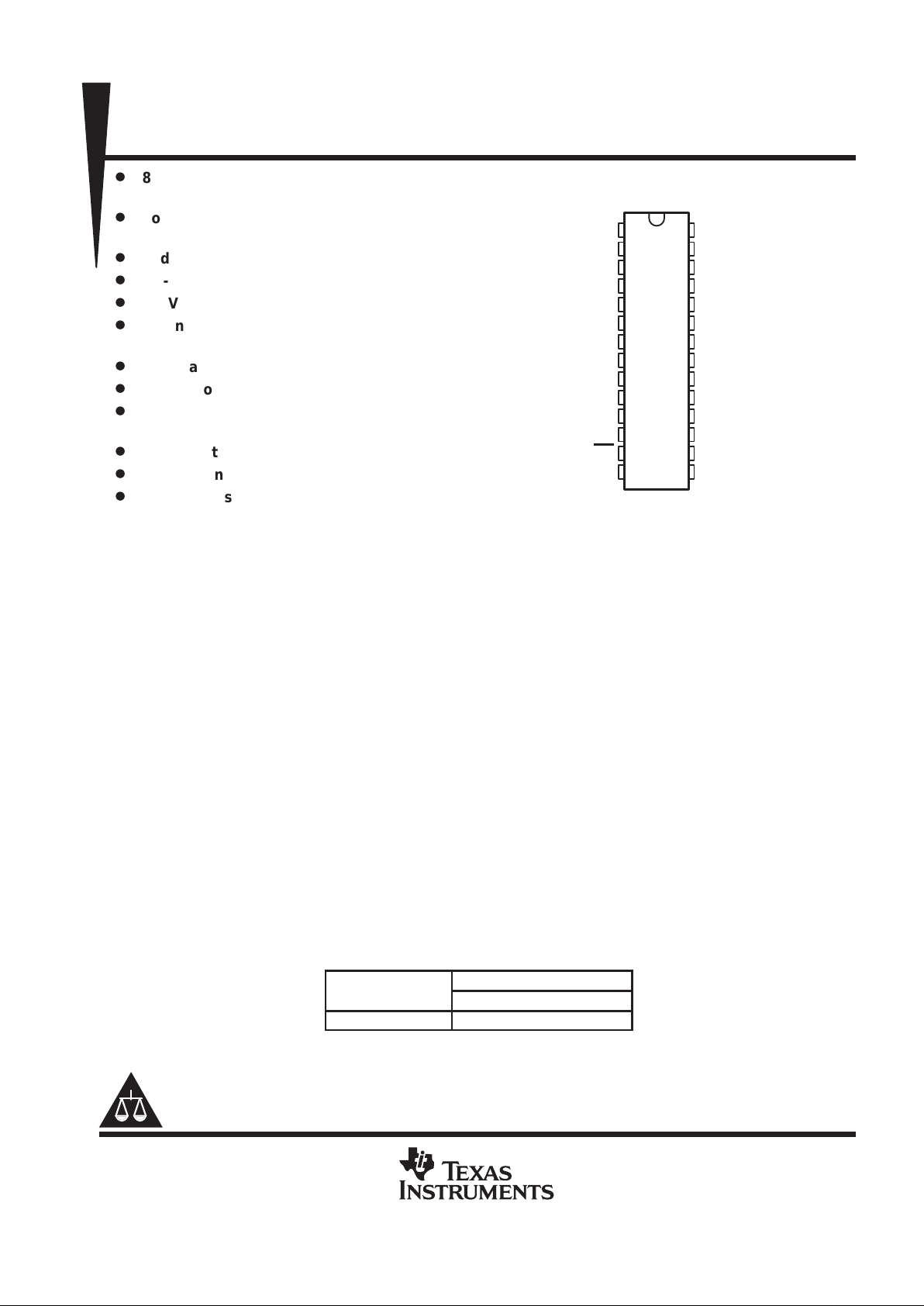
28-Pin Thin Shrink SOP (TSSOP) Packages
D
Applications
– Digital Communications (IF Sampling)
– High-Speed DSP Front-End
(TMS320C6000)
– Medical Imaging
– Video Processing (Scan Rate/Format
Conversion)
– DVD Read Channel Digitization
description
The TLV5535 is an 8-bit, 35 MSPS, high-speed A/D converter. It converts the analog input signal into 8-bit
binary-coded digital words up to a sampling rate of 35 MHz. All digital inputs and outputs are 3.3 V
TTL/CMOS-compatible.
The device consumes very little power due to the 3.3-V supply and an innovative single-pipeline architecture
implemented in a CMOS process. The user obtains maximum flexibility by setting both bottom and top voltage
references from user-supplied voltages. If no external references are available, on-chip references are
available for internal and external use. The full-scale range is 1 V
pp
up to 1.6 Vpp, depending on the analog
supply voltage. If external references are available, the internal references can be disabled independently from
the rest of the chip, resulting in an even greater power saving.
While usable in a wide variety of applications, the device is specifically suited for the digitizing of high-speed
graphics and for interfacing to LCD panels or LCD/DMD projection modules . Other applications include DVD
read channel digitization, medical imaging, and communications. This device is suitable for IF sampling of
communication systems using sub-Nyquist sampling methods because of its high analog input bandwidth.
AVAILABLE OPTIONS
PACKAGED DEVICES
T
A
TSSOP-28
–40°C to 85°C TLV5535IPW
PRODUCTION DATA information is current as of publication date.
Products conform to specifications per the terms of Texas Instruments
standard warranty. Production processing does not necessarily include
testing of all parameters.
Please be aware that an important notice concerning availability, standard warranty, and use in critical applications of
Texas Instruments semiconductor products and disclaimers thereto appears at the end of this data sheet.
1
2
3
4
5
6
7
8
9
10
11
12
13
14
28
27
26
25
24
23
22
21
20
19
18
17
16
15
DRV
DD
D0
D1
D2
D3
D4
D5
D6
D7
DRV
SS
DV
SS
CLK
OE
DV
DD
AV
SS
AV
DD
AIN
CML
PWDN_REF
AV
SS
REFBO
REFBI
REFTI
REFTO
AV
SS
BG
AV
DD
STBY
PW PACKAGE
(TOP VIEW)
Copyright 1999, Texas Instruments Incorporated
TLV5535
8-BIT, 35 MSPS, LOW-POWER ANALOG-TO-DIGITAL CONVERTER
SLAS221 – JUNE 1999
2
POST OFFICE BOX 655303 • DALLAS, TEXAS 75265
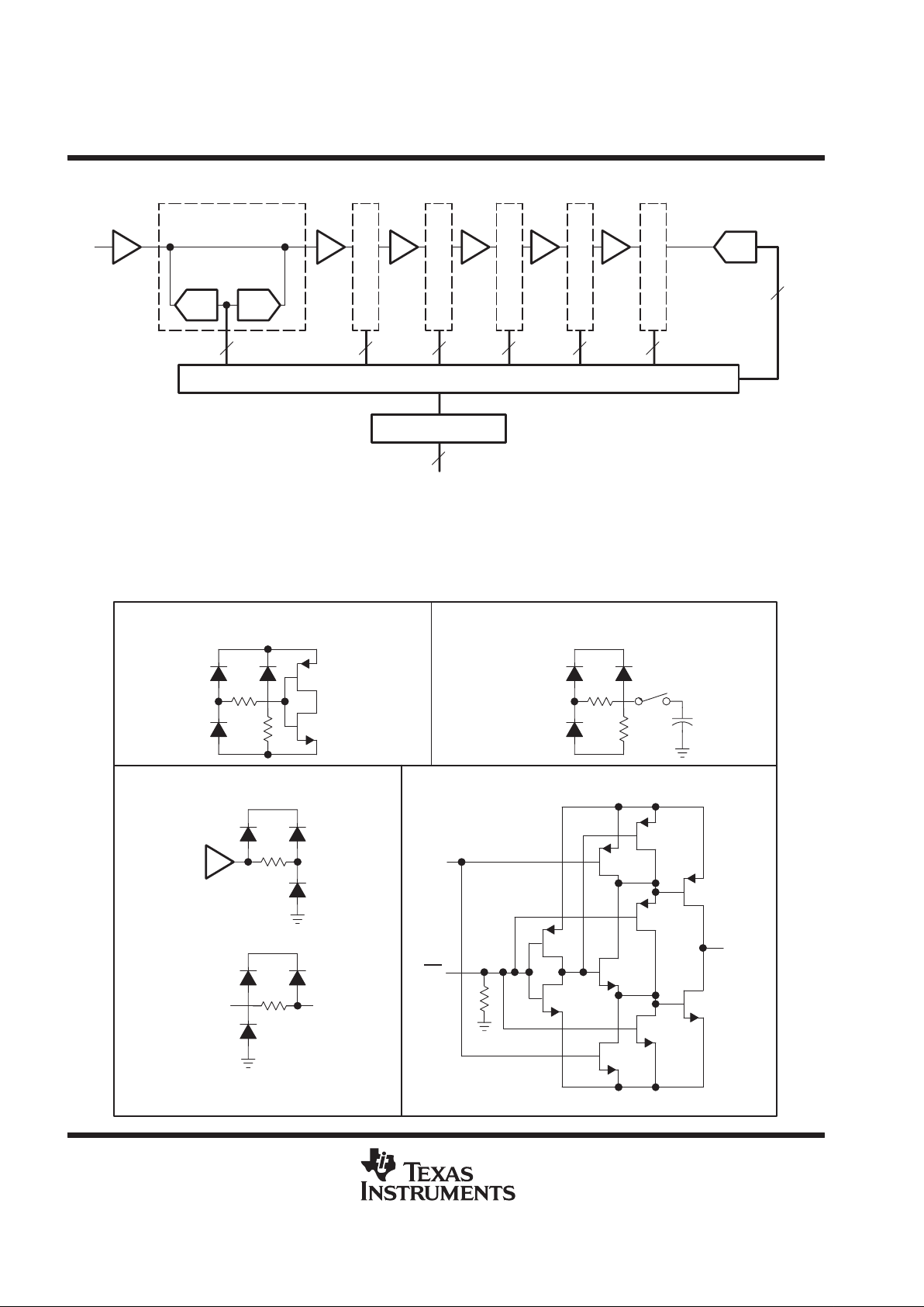
functional block diagram
SHA
DACADC
+
–
ADC
Correction Logic
Output Buffers
2222 2
D0(LSB)–D7(MSB)
2
2
SHA SHA SHA SHA SHA
The single-pipeline architecture uses 6 ADC/DAC stages and one final flash ADC. Each stage produces a
resolution of 2 bits. The correction logic generates its result using the 2-bit result from the first stage, 1 bit from
each of the 5 succeeding stages, and 1 bit from the final stage in order to arrive at an 8-bit result. The correction
logic ensures no missing codes over the full operating temperature range.
circuit diagrams of inputs and outputs
DV
DD
AV
DD
AV
DD
0.5 pF
Internal
Reference
Generator
REFTO
or
REFBO
AV
DD
REFBI
or
REFTI
OE
ALL DIGITAL INPUT CIRCUITS AIN INPUT CIRCUIT
REFERENCE INPUT CIRCUIT D0–D7 OUTPUT CIRCUIT
DRV
DD
DRV
SS
D_Out
D

TLV5535
8-BIT, 35 MSPS, LOW-POWER ANALOG-TO-DIGITAL CONVERTER
SLAS221 – JUNE 1999
3
POST OFFICE BOX 655303 • DALLAS, TEXAS 75265
Terminal Functions
TERMINAL
NAME NO.
I/O
DESCRIPTION
AIN 26 I Analog input
AV
DD
16, 27 I Analog supply voltage
AV
SS
18, 23, 28 I Analog ground
BG 17 O Band gap reference voltage. A 1-µF capacitor (with an optional 0.1-µF capacitor in parallel) should be
connected between this terminal and AVSS for external filtering.
CLK 12 I Clock input. The input is sampled on each rising edge of CLK.
CML 25 O Common mode level. This voltage is equal to (A VDD – AVSS) ÷ 2. An external 0.1-µF capacitor should be
connected between this terminal and AVSS.
D0 – D7 2 – 9 O Data outputs. D7 is the MSB.
DRV
DD
1 I Supply voltage for digital output drivers
DRV
SS
10 I Ground for digital output drivers
DV
DD
14 I Digital supply voltage
OE 13 I Output enable. When high, the D0 – D7 outputs go in high-impedance mode.
DV
SS
11 I Digital ground
PWDN_REF 24 I Power down for internal reference voltages. A high on this terminal disables the internal reference circuit.
REFBI 21 I Reference voltage bottom input. The voltage at this terminal defines the bottom reference voltage for the
ADC. It can be connected to REFBO or to an externally generated reference level. Sufficient filtering
should be applied to this input. The use of a 0.1-µF capacitor connected between REFBI and AVSS is
recommended. Additionaly, a 0.1-µF capacitor can be connected between REFTI and REFBI.
REFBO 22 O Reference voltage bottom output. An internally generated reference is available at this terminal. It can be
connected to REFBI or left unconnected. A 1-µF capacitor between REFBO and A VSS provides sufficient
decoupling required for this output.
REFTI 20 I Reference voltage top input. The voltage at this terminal defines the top reference voltage for the ADC.
It can be connected to REFTO or to an externally generated reference level. Sufficient filtering should be
applied to this input. The use of a 0.1-µF capacitor between REFTI and AVSS is recommended.
Additionaly, a 0.1-µF capacitor can be connected between REFTI and REFBI.
REFTO 19 O Reference voltage top output. An internally generated reference is available at this terminal. It can be
connected to REFTI or left unconnected. A 1-µF capacitor between REFTO and A VSS provides sufficient
decoupling required for this output.
STBY 15 I Standby input. A high level on this input enables power-down mode.
absolute maximum ratings over operating free-air temperature (unless otherwise noted)
†
Supply voltage range:AVDD to AVSS, DVDD to DVSS –0.5 V to 4.5 V. . . . . . . . . . . . . . . . . . . . . . . . . . . . . . . . . .
AVDD to DVDD, AVSS to DVSS –0.5 V to 0.5 V. . . . . . . . . . . . . . . . . . . . . . . . . . . . . . . . . .
Digital input voltage range to DVSS –0.5 V to DVDD + 0.5 V. . . . . . . . . . . . . . . . . . . . . . . . . . . . . . . . . . . . . . . . . .
Analog input voltage range to AVSS –0.5 V to AVDD + 0.5 V. . . . . . . . . . . . . . . . . . . . . . . . . . . . . . . . . . . . . . . . .
Digital output voltage range applied from external source to DGND –0.5 V to DV
DD
+ 0.5 V. . . . . . . . . . . . . .
Reference voltage input range to AGND: V
(REFTI)
, V
(REFTO)
, V
(REFBI)
, V
(REFBO)
–0.5 V to AVDD + 0.5 V
Operating free-air temperature range, TA: TLV5535I –40°C to 85°C. . . . . . . . . . . . . . . . . . . . . . . . . . . . . . . . . .
Storage temperature range, T
stg
–55°C to 150°C. . . . . . . . . . . . . . . . . . . . . . . . . . . . . . . . . . . . . . . . . . . . . . . . . . .
†
Stresses beyond those listed under “absolute maximum ratings” may cause permanent damage to the device. These are stress ratings only, and
functional operation of the device at these or any other conditions beyond those indicated under “recommended operating conditions” is not
implied. Exposure to absolute-maximum-rated conditions for extended periods may affect device reliability.
TLV5535
8-BIT, 35 MSPS, LOW-POWER ANALOG-TO-DIGITAL CONVERTER
SLAS221 – JUNE 1999
4
POST OFFICE BOX 655303 • DALLAS, TEXAS 75265
recommended operating conditions over operating free-temperature range
power supply
MIN NOM MAX UNIT
AVDD – AV
SS
Supply voltage
DVDD – DV
SS
3 3.3 3.6 V
DRVDD – DRV
SS
analog and reference inputs
MIN NOM MAX UNIT
Reference input voltage (top), V
(REFTI)
(NOM) – 0.2 2 + (AVDD – 3) (NOM) + 0.2 V
Reference input voltage (bottom), V
(REFBI)
0.8 1 1.2 V
Reference voltage differential, V
(REFTI)
– V
(REFBI)
1 + (AVDD – 3) V
Analog input voltage, V
(AIN)
V
(REFBI)
V
(REFTI)
V
digital inputs
MIN NOM MAX UNIT
High-level input voltage, V
IH
2.0 DV
DD
V
Low-level input voltage, V
IL
DGND 0.2xDV
DD
V
Clock period, t
c
28.6 ns
Pulse duration, clock high, t
w(CLKH)
13 ns
Pulse duration, clock low, t
w(CLKL)
13 ns
electrical characteristics over recommended operating conditions, f
CLK
= 35 MSPS, external
voltage references (unless otherwise noted)
power supply
PARAMETER TEST CONDITIONS MIN TYP MAX UNIT
AV
DD
27 34
I
DD
Operating supply current
DV
DD
AVDD = DVDD = 3.3 V, DRVDD = 3 V,
p
–
-
1.5 2.6
mA
DRV
DD
C
L
= 15 F,
V
I
= 1
MHz
, –1-dB
FS
4 6
p
PWDN_REF = L 106 139
PDPower dissipation
PWDN_REF = H 90 113
mW
P
D(STBY)
Standby power STBY = H, CLK held high or low 11 15
digital logic inputs
PARAMETER TEST CONDITIONS MIN TYP MAX UNIT
I
IH
High-level input current on CLK
†
AVDD = DVDD = DRVDD = CLK = 3.6 V 10 µA
I
IL
Low-level input current on digital inputs
(OE
, STDBY, PWDN_REF, CLK)
AVDD = DVDD = DRVDD = 3.6 V,
Digital inputs at 0 V
10 µA
CIInput capacitance 5 pF
†
IIH leakage current on other digital inputs (OE, STDBY , PWDN_REF) is not measured since these inputs have an internal pull-down resistor of
4 KΩ to DGND.
TLV5535
8-BIT, 35 MSPS, LOW-POWER ANALOG-TO-DIGITAL CONVERTER
SLAS221 – JUNE 1999
5
POST OFFICE BOX 655303 • DALLAS, TEXAS 75265
electrical characteristics over recommended operating conditions, f
CLK
= 35 MSPS, external
voltage references (unless otherwise noted) (continued)
logic outputs
PARAMETER TEST CONDITIONS MIN TYP MAX UNIT
V
OH
High-level output voltage
AVDD = DVDD = DRVDD = 3 V at IOH = 50 µA,
Digital output forced high
2.8 V
V
OL
Low-level output voltage
AVDD = DVDD = DRVDD = 3.6 V at IOL = 50 µA,
Digital output forced low
0.1 V
C
O
Output capacitance 5 pF
I
OZH
High-impedance state output current to
high level
10 µA
I
OZL
High-impedance state output current to
low level
AV
DD
=
DV
DD
=
DRV
DD
= 3.6
V
10 µA
dc accuracy
PARAMETER TEST CONDITIONS MIN TYP MAX UNIT
TA = 25°C –1.5 ±0.7 1.5 LSB
Integral nonlinearity (INL), best-fit
Internal references (see Note 1)
TA = –40°C to 85°C –2.4 ±0.7 2.4 LSB
Differential nonlinearity (DNL) Internal references (see Note 2), TA = –40°C to 85°C –1 ±0.6 1.3 LSB
Zero error
AVDD = DVDD = 3.3 V, DRVDD = 3 V,
5 %FS
Full-scale error
DD DD DD
Internal references (see Note 3)
5 %FS
NOTES: 1. Integral nonlinearity refers to the deviation of each individual code from a line drawn from zero to full scale. The point used as zero
occurs 1/2 LSB before the first code transition. The full-scale point is defined as a level 1/2 LSB beyond the last code transition. The
deviation is measured from the center of each particular code to the true straight line between these two endpoints.
2. An ideal ADC exhibits code transitions that are exactly 1 LSB apart. DNL is the deviation from this ideal value. Therefore this measure
indicates how uniform the transfer function step sizes are. The ideal step size is defined here as the step size for the device under
test [i.e., (last transition level – first transition level) ÷ (2n – 2)]. Using this definition for DNL separates the effects of gain and offset
error. A minimum DNL better than –1 LSB ensures no missing codes.
3. Zero error is defined as the difference in analog input voltage – between the ideal voltage and the actual voltage – that switches
the ADC output from code 0 to code 1. The ideal voltage level is determined by adding the voltage corresponding to 1/2 LSB to the
bottom reference level. The voltage corresponding to 1 LSB is found from the difference of top and bottom references divided by
the number of ADC output levels (256).
Full-scale error is defined as the difference in analog input voltage – between the ideal voltage and the actual voltage – that switches
the ADC output from code 254 to code 255. The ideal voltage level is determined by subtracting the voltage corresponding to 1.5
LSB from the top reference level. The voltage corresponding to 1 LSB is found from the difference of top and bottom references
divided by the number of ADC output levels (256).
analog input
PARAMETER TEST CONDITIONS MIN TYP MAX UNIT
C
I
Input capacitance 4 pF
TLV5535
8-BIT, 35 MSPS, LOW-POWER ANALOG-TO-DIGITAL CONVERTER
SLAS221 – JUNE 1999
6
POST OFFICE BOX 655303 • DALLAS, TEXAS 75265
electrical characteristics over recommended operating conditions, f
CLK
= 35 MSPS, external
voltage references (unless otherwise noted) (continued)
reference input (AVDD = DVDD = DRVDD = 3.6 V)
PARAMETER TEST CONDITIONS MIN TYP MAX UNIT
R
ref
Reference input resistance 400 Ω
I
ref
Reference input current 2.5 mA
reference outputs
PARAMETER TEST CONDITIONS MIN TYP MAX UNIT
V
(REFTO)
Reference top offset voltage
Absolute min/max values valid
2.07 2 + [(AVDD – 3) ÷ 2] 2.21 V
V
(REFBO)
Reference bottom offset voltage
and tested for AVDD = 3.3 V
1.09 1 + [(AVDD – 3) ÷ 2] 1.21 V
dynamic performance
†
PARAMETER TEST CONDITIONS MIN TYP MAX UNIT
fin = 1 MHz 6.6 7.4
Effective number of bits (ENOB)
fin = 4.2 MHz 6.6 7.4
Bits
fin = 15 MHz 7
fin = 1 MHz 41.5 46
Signal-to-noise ratio + distortion (SNRD)
fin = 4.2 MHz 41.5 46
dB
fin = 15 MHz 43
fin = 1 MHz –46 –55
Total harmonic distortion (THD)
fin = 4.2 MHz –45.5 –54
dB
fin = 15 MHz –50
fin = 1 MHz 48 58
Spurious free dynamic range (SFDR)
fin = 4.2 MHz 48 58
dB
fin = 15 MHz 52
Analog input full-power bandwidth, BW See Note 4 600 MHz
p
Differential phase, DP
f
CLK
= 35 MHz, fin = 4.2 MHz,
0.6
CLK in
20 IRE amplitude vs full-scale of 140 IRE
Differential gain, DG
20 IRE am litude vs full scale of 140 IRE
0.2%
†
Based on analog input voltage of – 1-dB FS referenced to a 1.3 Vpp full-scale input range and using the external voltage references at
f
CLK
= 35 MSPS with AVDD = DVDD = 3.3 V and DRVDD = 3 V at 25°C.
NOTE 4: The analog input bandwidth is defined as the maximum frequency of a –1-dB FS input sine that can be applied to the device for which
an extra 3-dB attenuation is observed in the reconstructed output signal.
TLV5535
8-BIT, 35 MSPS, LOW-POWER ANALOG-TO-DIGITAL CONVERTER
SLAS221 – JUNE 1999
7
POST OFFICE BOX 655303 • DALLAS, TEXAS 75265
electrical characteristics over recommended operating conditions, f
CLK
= 35 MSPS, external
voltage references (unless otherwise noted) (continued)
timing requirements
PARAMETER TEST CONDITIONS MIN TYP MAX UNIT
Maximum conversion rate 35 MHz
f
CLK
Minimum conversion rate 10 kHz
t
d(o)
Output delay time (see Figure 1) CL = 10 pF, See Notes 5 and 6 9 ns
t
h(o)
Output hold time CL = 2 pF, See Note 5 2 ns
t
d(pipe)
Pipeline delay time (latency) See Note 6 4.5 4.5 4.5
CLK
cycles
t
d(a)
Aperture delay time 3 ns
t
j(a)
Aperture jitter
1.5 ps, rms
t
dis
Disable time, OE rising to Hi-Z
See Note 5
5 8 ns
t
en
Enable time, OE falling to valid data 5 8 ns
NOTES: 5. Output timing t
d(o)
is measured from the 1.5 V level of the CLK input falling edge to the 10%/90% level of the digital output. The digital
output load is not higher than 10 pF.
Output hold time t
h(o)
is measured from the 1.5 V level of the CLK input falling edge to the 10%/90% level of the digital output. The
digital output is load is not less than 2 pF.
Aperture delay t
d(A)
is measured from the 1.5 V level of the CLK input to the actual sampling instant.
The OE signal is asynchronous.
OE timing t
dis
is measured from the V
IH(MIN)
level of OE to the high-impedance state of the output data. The digital output load is
not higher than 10 pF.
OE timing ten is measured from the V
IL(MAX)
level of OE to the instant when the output data reaches V
OH(min)
or V
OL(max)
output
levels. The digital output load is not higher than 10 pF.
6. The number of clock cycles between conversion initiation on an input sample and the corresponding output data being made
available from the ADC pipeline. Once the data pipeline is full, new valid output data is provided on every clock cycle. In order to
know when data is stable on the output pins, the output delay time t
d(o)
(i.e., the delay time through the digital output buffers) needs
to be added to the pipeline latency. Note that since the max t
d(o)
is more than 1/2 clock period at 35 MHz, data cannot be reliably
clocked in on a rising edge of CLK at this speed. The falling edge should be used.
TLV5535
8-BIT, 35 MSPS, LOW-POWER ANALOG-TO-DIGITAL CONVERTER
SLAS221 – JUNE 1999
8
POST OFFICE BOX 655303 • DALLAS, TEXAS 75265
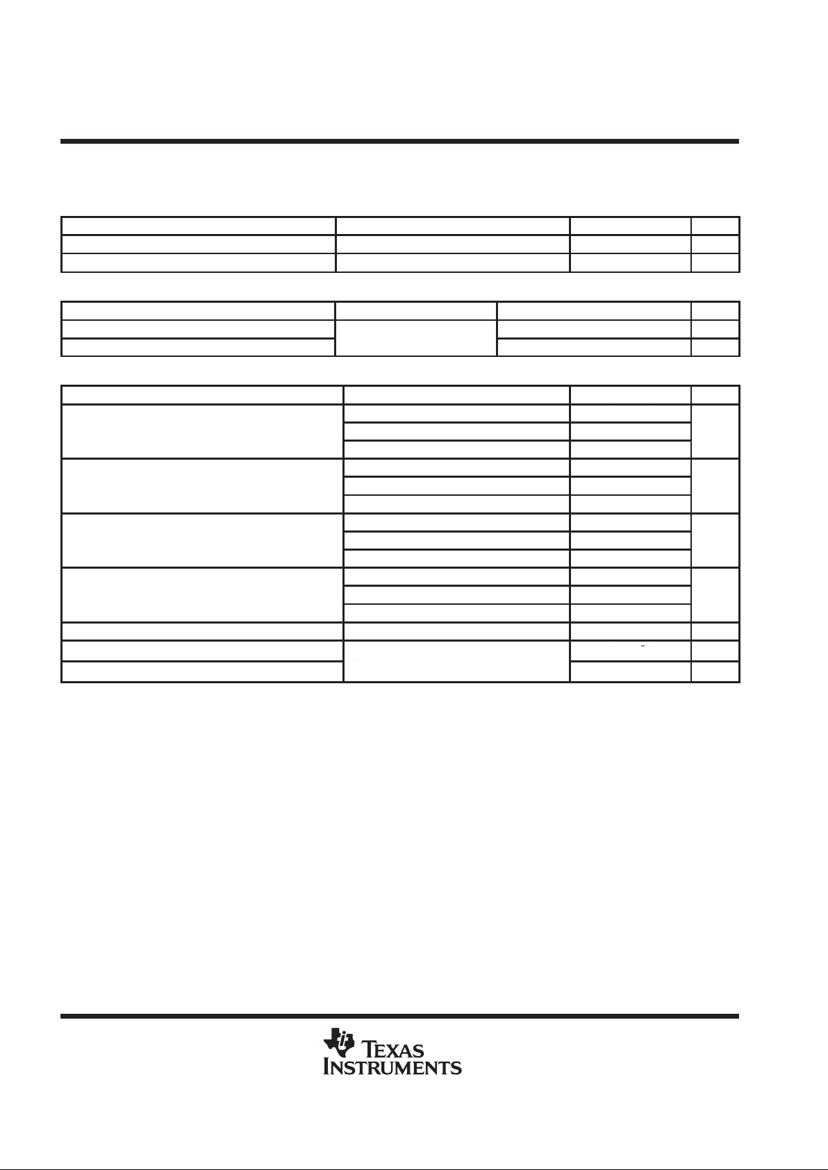
PARAMETER MEASUREMENT INFORMATION
D0–D7 N–4 N–3 N–2 N–1 N N+1
N
N+1
N+2
N+3
N+4
N+5
t
j(a)
t
d(a)
V
IL
(max)
1.5 V
t
w(CLKH)
t
w(CLKL)
1/f
CLK
t
h(o)
1.5 V
t
d(o)
t
dis
t
en
CLK
OE
90%
10%
V
IH(min)
t
d(pipe)
V
OH(min)
V
OL(max)
V
IL(max)
V
IH
(min)
Figure 1. Timing Diagram
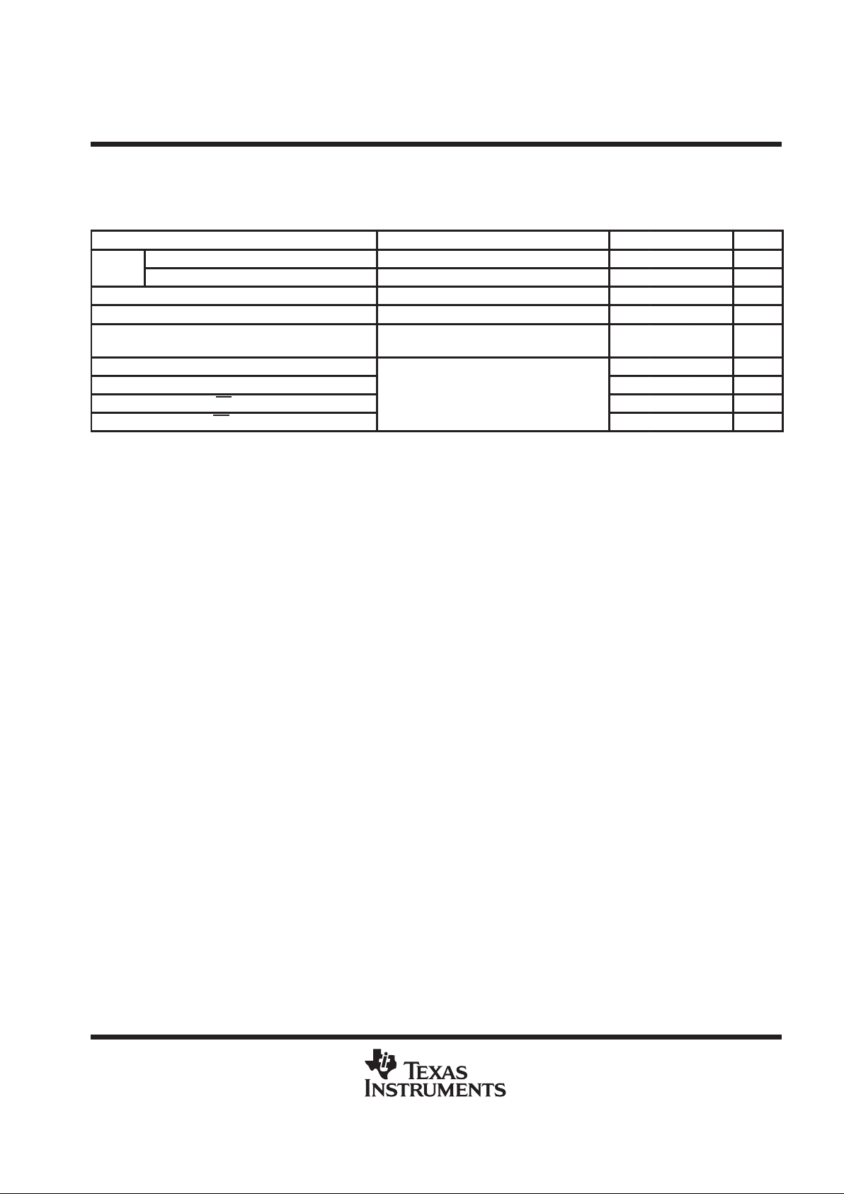
TYPICAL CHARACTERISTICS
performance plots at 25°C
–0.2
–0.1
0.0
0.1
0.2
0 50 100 150 200 250
DNL – LSB
ADC Code
Figure 2. DNL vs Input Code at 35 MSPS (with external reference, PW Package)
TLV5535
8-BIT, 35 MSPS, LOW-POWER ANALOG-TO-DIGITAL CONVERTER
SLAS221 – JUNE 1999
9
POST OFFICE BOX 655303 • DALLAS, TEXAS 75265
TYPICAL CHARACTERISTICS
performance plots at 25°C (continued)
–0.4
–0.3
–0.2
–0.1
–0.0
0.1
0.2
0.3
0.4
0 50 100 150 200 250
INL – LSB
ADC Code
Figure 3. INL vs Input Code at 35 MSPS (with external reference, PW package)
0
5
10
15
20
25
30
35
40
45
50
0 1020304050
SNRD – dB
Analog Input Frequency – MHz
Figure 4. SNRD vs fin at 35 MSPS (external reference)
TLV5535
8-BIT, 35 MSPS, LOW-POWER ANALOG-TO-DIGITAL CONVERTER
SLAS221 – JUNE 1999
10
POST OFFICE BOX 655303 • DALLAS, TEXAS 75265
TYPICAL CHARACTERISTICS
performance plots at 25°C (continued)
0
1
2
3
4
5
6
7
8
0 1020304050
ENOB
Analog Input Frequency – MHz
Figure 5. ENOB vs FIN, 35 MSPS (external reference)
–100
–90
–80
–70
–60
–50
–40
–30
–20
–10
0
0 5 10 15
Power – dBFS
f – Frequency – MHz
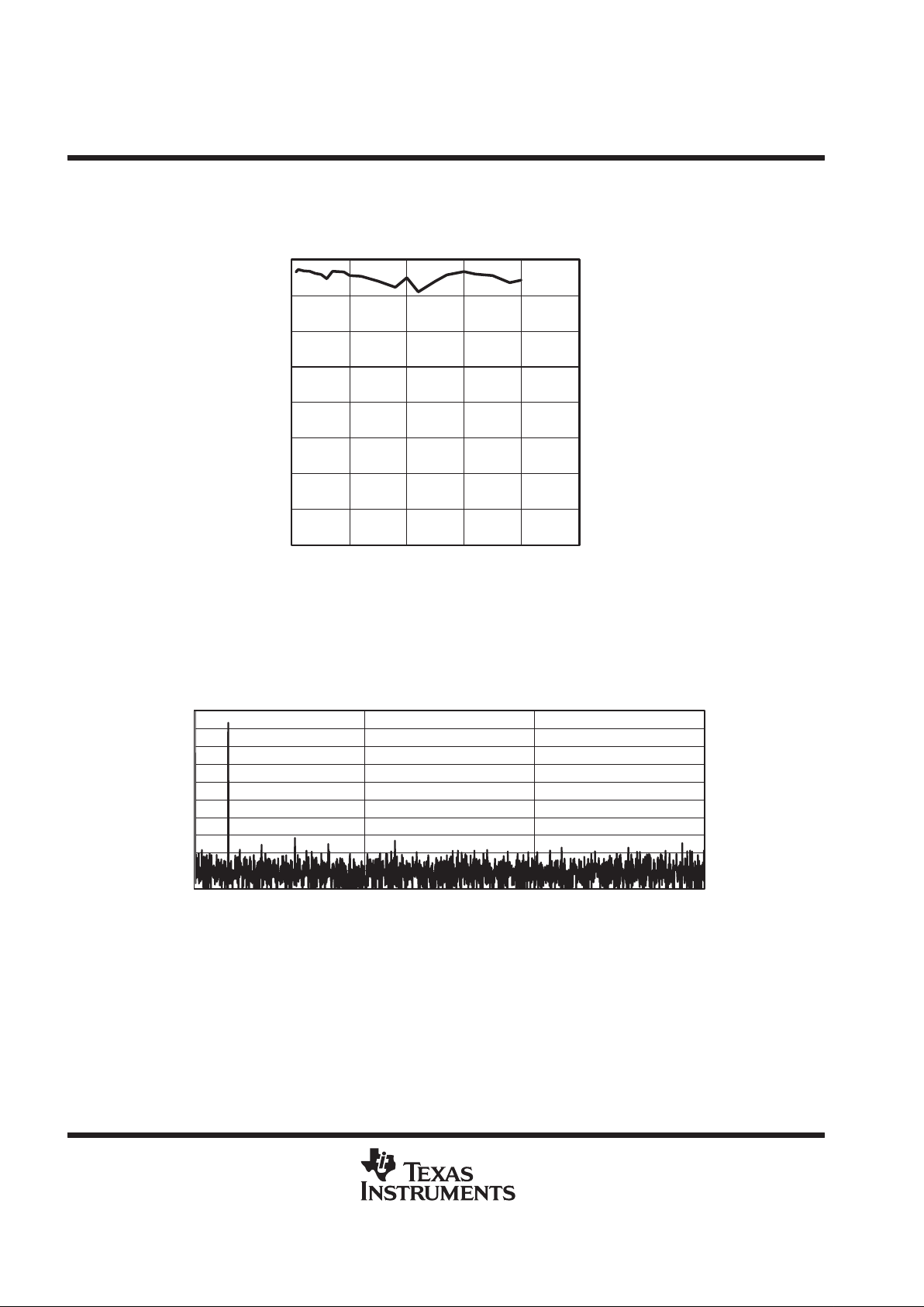
Figure 6. Spectral Plot fin = 1.0 MHz at 35 MSPS

TLV5535
8-BIT, 35 MSPS, LOW-POWER ANALOG-TO-DIGITAL CONVERTER
SLAS221 – JUNE 1999
11
POST OFFICE BOX 655303 • DALLAS, TEXAS 75265
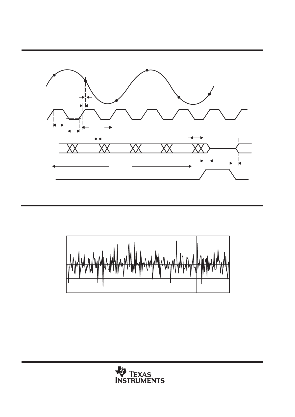
TYPICAL CHARACTERISTICS
performance plots at 25°C (continued)
Power – dB
f – Frequency – MHz
–100
–90
–80
–70
–60
–50
–40
–30
–20
–10
0
0 5 10 15
Figure 7. Spectral Plot fin = 4.2 MHz at 35 MSPS
–100
–90
–80
–70
–60
–50
–40
–30
–20
–10
0
0 5 10 15
Power – dB
f – Frequency – MHz
Figure 8. Spectral Plot fin = 15.527 MHz at 35 MSPS
TLV5535
8-BIT, 35 MSPS, LOW-POWER ANALOG-TO-DIGITAL CONVERTER
SLAS221 – JUNE 1999
12
POST OFFICE BOX 655303 • DALLAS, TEXAS 75265
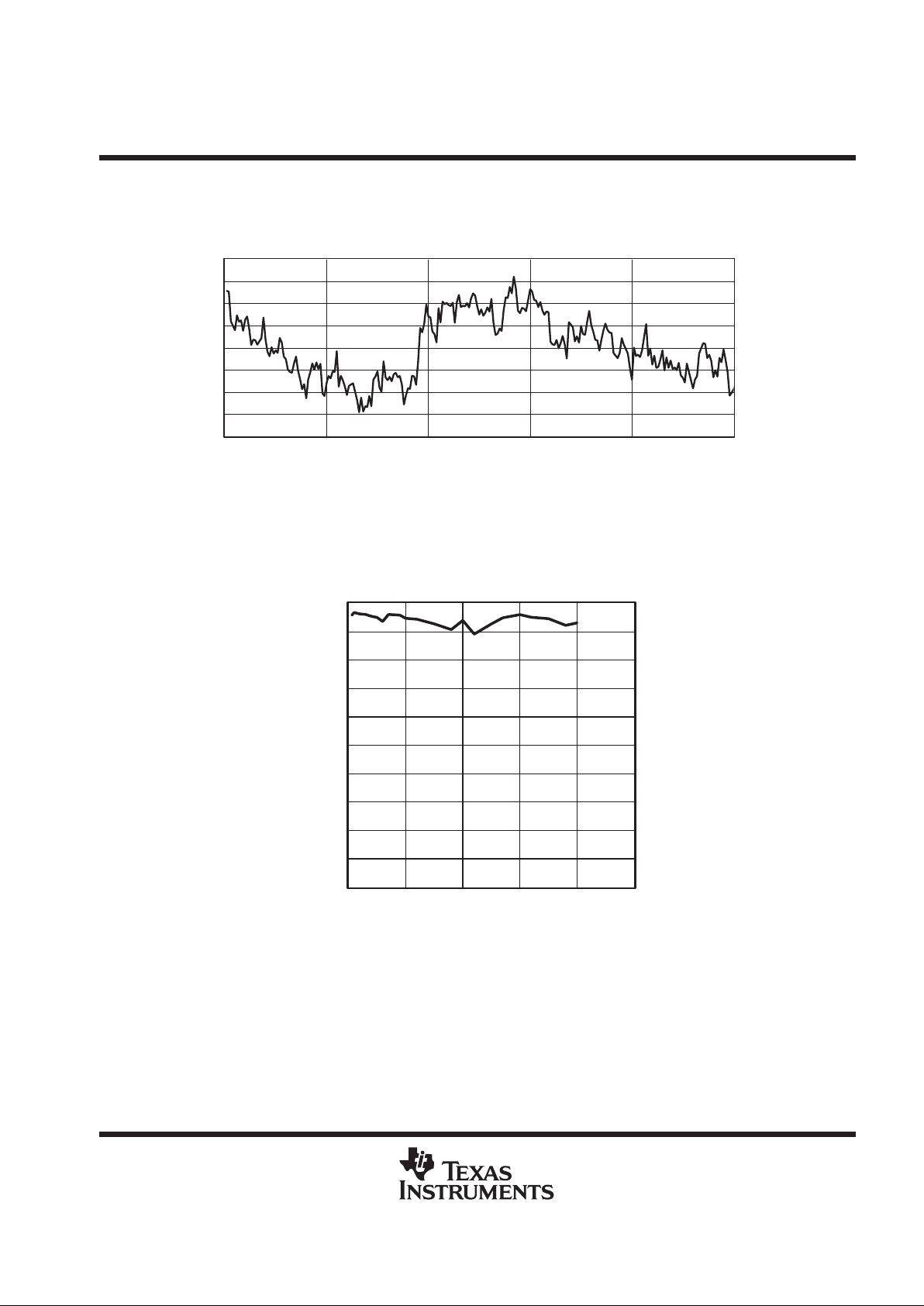
TYPICAL CHARACTERISTICS
performance plots at 25°C (continued)
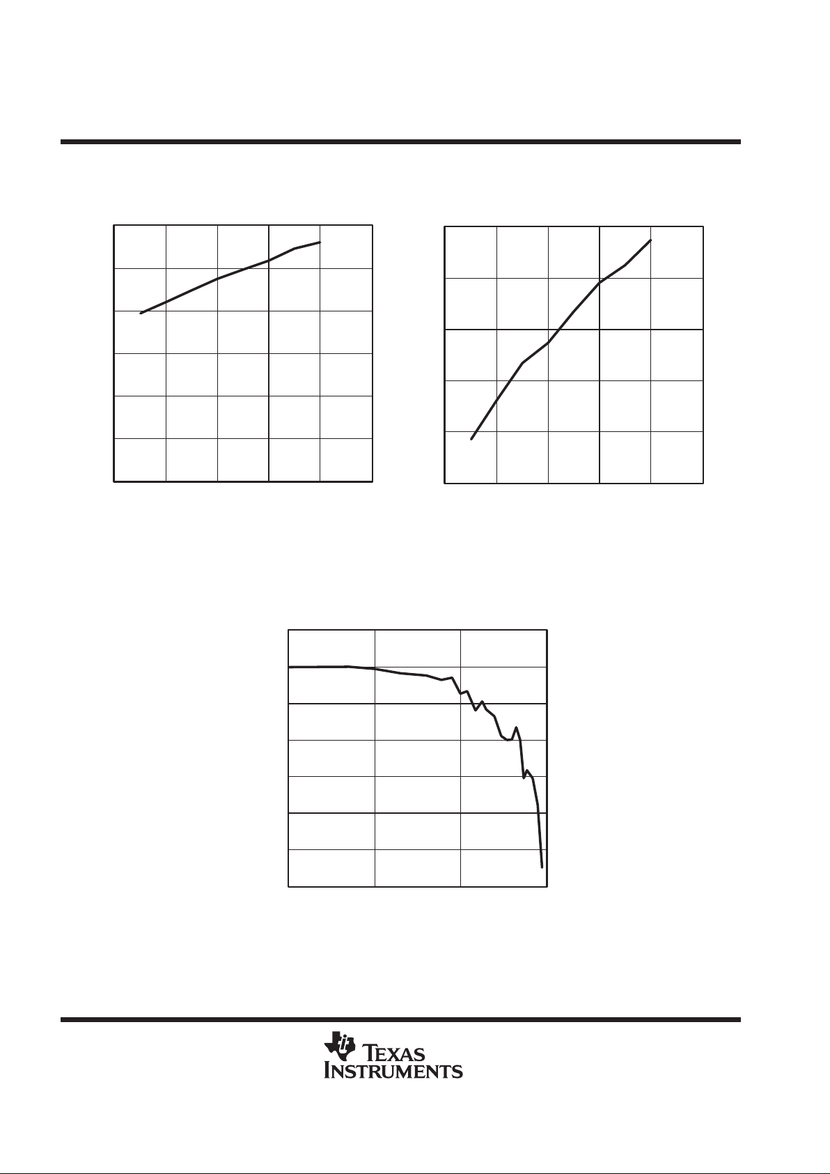
Figure 9. Power vs f
CLK
at fin = 1 MHz, –1-dB FS
Figure 10. DRVDD Supply Current vs f
CLK
at fin = 1 MHz, –1-dB FS
0
20
40
60
80
100
120
0 1020304050
Power – mV
Input Clock Frequency – MHz
0
0.5
1.0
1.5
2.0
2.5
0 1020304050
Input Frequency – MHz
Supply Current – mA
–7.00
–6.00
–5.00
–4.00
–3.00
–2.00
–1.00
0.00
1 10 100 1000
Fundamental – dB
Input Frequency – MHz
Figure 11. ADC Output Power With Respect to –1-dB FS V
IN
(internal reference, PW package)

TLV5535
8-BIT, 35 MSPS, LOW-POWER ANALOG-TO-DIGITAL CONVERTER
SLAS221 – JUNE 1999
13
POST OFFICE BOX 655303 • DALLAS, TEXAS 75265
PRINCIPLES OF OPERATION
The TL V5535 implements a high-speed 35 MSPS converter in a cost-effective CMOS process. Powered from
3.3 V , the single-pipeline design architecture ensures low-power operation and 8-bit accuracy . Signal input and
clock signals are all single-ended. The digital inputs are 3.3-V TTL/CMOS compatible. Internal voltage
references are included for both bottom and top voltages. Therefore the converter forms a self-contained
solution. Alternatively , the user may apply externally generated reference voltages. In doing so, both input offset
and input range can be modified to suit the application.
A high-speed sampling-and-hold captures the analog input signal. Multiple stages generate the output code with
a pipeline delay of 4.5 CLK cycles. Correction logic combines the multistage data and aligns the 8-bit output
word. All digital logic operates at the rising edge of CLK.
analog input
A first-order approximation for the equivalent analog input circuit of the TLV5535 is shown in Figure 12. The
equivalent input capacitance C
I
is 4 pF typical. The input must charge/discharge this capacitance within the
sample period of one half clock cycle. When a full-scale voltage step is applied, the input source provides the
charging current through the switch resistance RSW (200 Ω) of S1 and quickly settles. In this case, the input
impedance is low. Alternatively, when the source voltage equals the value previously stored on CI, the hold
capacitor requires no input current and the equivalent input impedance is very high.
To maintain the frequency performance outlined in the specifications, the total source impedance should be
limited to about 80 Ω, as follows from the equation with f
CLK
= 35 MHz, CI = 4 pF, RSW = 200 Ω:
RStƪ1 ÷ǒ2f
CLK
CI
In(256)Ǔ–R
SW
ƫ
The source impedance is approximatly 450 Ω.

TLV5535
8-BIT, 35 MSPS, LOW-POWER ANALOG-TO-DIGITAL CONVERTER
SLAS221 – JUNE 1999
14
POST OFFICE BOX 655303 • DALLAS, TEXAS 75265
PRINCIPLE OF OPERATION
analog input (continued)
So, for applications running at a lower f
CLK
, the total source resistance will increase proportionally.
AIN
C
I
S1
R
SW
R
S
V
S
TLV5535
Figure 12. Simplified Equivalent Input Circuit
dc coupled input
For dc-coupled systems an op amp can level-shift a ground-referenced input signal. A circuit as shown in
Figure 13(a) is acceptable. Alternatively , the user might want a bipolar shift together with the bottom reference
voltage as seen in Figure 13(b). In this case the AIN voltage is given by:
AIN+2 R2÷ǒR1)
R
2
Ǔ
V
REF
–V
IN
_
+
AV
DD
V
IN
REFTI
REFTO
REFBI
REFBO
AIN
TLV5535
_
+
V
REF
V
IN
REFTI
REFTO
REFBI
REFBO
AIN
TLV5535
R
IN
R
1
R
IN
R
2
(a)
(b)
Figure 13. DC-Coupled Input Circuit
ac coupled input
For many applications, especially in single supply operation, ac coupling offers a convenient way for biasing
the analog input signal at the proper signal range. Figure 14 shows a typical configuration. To maintain the
outlined specifications, the component values need to be carefully selected. The most important issue is the
positioning of the 3-dB high-pass corner point f
–3 dB
, which is a function of R2 and the parallel combination of
C1 and C2, called Ceq. This is given by the following equation:
f
–3 dB
+
1 ÷ǒ2π xR2xC
eq
Ǔ
where Ceq is the parallel combination of C1 and C2.
Since C1 is typically a large electrolytic or tantalum capacitor, the impedance becomes inductive at higher
frequencies. Adding a small ceramic or polystyrene capacitor, C2 of approximately 0.01 µF, which is not
inductive within the frequency range of interest, maintains low impedance. If the minimum expected input signal
frequency is 20 kHz, and R2 equals 1 kΩ and R1 equals 50 Ω, the parallel capacitance of C1 and C2 must be
a minimum of 8 nF to avoid attenuating signals close to 20 kHz.

TLV5535
8-BIT, 35 MSPS, LOW-POWER ANALOG-TO-DIGITAL CONVERTER
SLAS221 – JUNE 1999
15
POST OFFICE BOX 655303 • DALLAS, TEXAS 75265
PRINCIPLE OF OPERATION
ac coupled input (continued)
V
IN
AIN
TLV5535
R1
R2
V
BIAS
+
–
C1
C2
Figure 14. AC-Coupled Input Circuit
reference terminals
The voltages on terminals REFBI and REFTI determine the TLV5535 input range. Since the device has an
internal voltage reference generator with outputs available on REFBO and REFTO respectively , corresponding
terminals can be directly connected externally to provide a contained ADC solution. Especially at higher
sampling rates, it is advantageous to have a wider analog input range. The wider analog input range is
achievable by using external voltage references (e.g., at AV
DD
= 3.3 V, the full-scale range can be extended
from 1 Vpp (internal reference) to 1.3 Vpp (external reference) as shown in T able 1). These voltages should not
be derived via a voltage divider from a power supply source. Instead, a bandgap-derived voltage reference
should be used to derive both references via an op amp circuit. Refer to the schematic of the TL V5535 evaluation
module for an example circuit.
When using external references, the full-scale ADC input range and its dc position can be adjusted. The
full-scale ADC range is always equal to V
REFT
– V
REFB
. The maximum full-scale range is dependent on A V
DD
as shown in the specification section. In addition to the limitation on their difference, V
REFT
and V
REFB
each also
have limits on their useful range. These limits are also dependent on AVDD.
Table 1 summarizes these limits for 3 cases.
Table 1. Recommended Operating Modes
AV
DD
V
REFB(min)VREFB(max)VREFT(min)VREFT(max)
(V
REFT–VREFB)max
3 V 0.8 V 1.2 V 1.8 V 2.2 V 1 V
3.3 V 0.8 V 1.2 V 2.1 V 2.5 V 1.3 V
3.6 V 0.8 V 1.2 V 2.4 V 2.8 V 1.6 V
digital inputs
The digital inputs are CLK, STDBY, PWDN_REF, and OE. All of these signals, except CLK, have an internal
pulldown resistor to connect to digital ground. This provides a default active operation mode using internal
references when left unconnected.

TLV5535
8-BIT, 35 MSPS, LOW-POWER ANALOG-TO-DIGITAL CONVERTER
SLAS221 – JUNE 1999
16
POST OFFICE BOX 655303 • DALLAS, TEXAS 75265
PRINCIPLE OF OPERATION
digital inputs (continued)
The CLK signal at high frequencies should be considered as an analog input. Overshoot/undershoot should be
minimized by proper termination of the signal close to the TLV5535. An important cause of performance
degradation for a high-speed ADC is clock jitter. Clock jitter causes uncertainty in the sampling instant of the
ADC, in addition to the inherent uncertainty on the sampling instant caused by the part itself, as specified by
its aperture jitter. There is a theoretical relationship between the frequency (f) and resolution (2
N
) of a signal
that needs to be sampled and the maximum amount of aperture error dt
max
that is tolerable. The following
formula shows the relation:
dt
max
+1Bƪp
f2
ǒ
N)1
Ǔ
ƫ
As an example, for an 8-bit converter with a 15-MHz input, the jitter needs to be kept < 41 pF in order not to have
changes in the LSB of the ADC output due to the total aperture error.
digital outputs
The output of the TL V5535 is standard binary code. Capacitive loading on the output should be kept as low as
possible (a maximum loading of 10 pF is recommended) to provide the best performance. Higher output loading
causes higher dynamic output currents and can increase noise coupling into the analog front end of the device.
To drive higher loads, the use of an output buffer is recommended.
When clocking output data from the TL V5535, it is important to observe its timing relation to CLK. The pipeline
ADC delay is 4.5 clock cycles to which the maximum output propagation delay is added. See Note 6 in the
specification section for more details.
layout, decoupling and grounding rules
It is necessary for any PCB using the TLV5535 to have proper grounding and layout to achieve the stated
performance. Separate analog and digital ground planes that are spliced underneath the device are advisable.
The TLV5535 has digital and analog terminals on opposite sides of the package to make proper grounding
easier. Since there is no internal connection between the analog and digital grounds, they have to be joined on
the PCB. Joining the digital and analog grounds at a point in close proximity to the TLV5535 is advised.
As for power supplies, separate analog and digital supply terminals are provided on the device (A V
DD
/DVDD).
The supply to the digital output drivers is kept separate also (DRVDD). Lowering the voltage on this supply from
the nominal 3.3 V to 3 V improves performance because of the lower switching noise caused by the output
buffers.
Due to the high sampling rate and switched-capacitor architecture, the TLV5535 generates transients on the
supply and reference lines. Proper decoupling of these lines is essential. Decoupling as shown in the schematic
of the TLV5535 EVM is recommended.

TLV5535
8-BIT, 35 MSPS, LOW-POWER ANALOG-TO-DIGITAL CONVERTER
SLAS221 – JUNE 1999
17
POST OFFICE BOX 655303 • DALLAS, TEXAS 75265
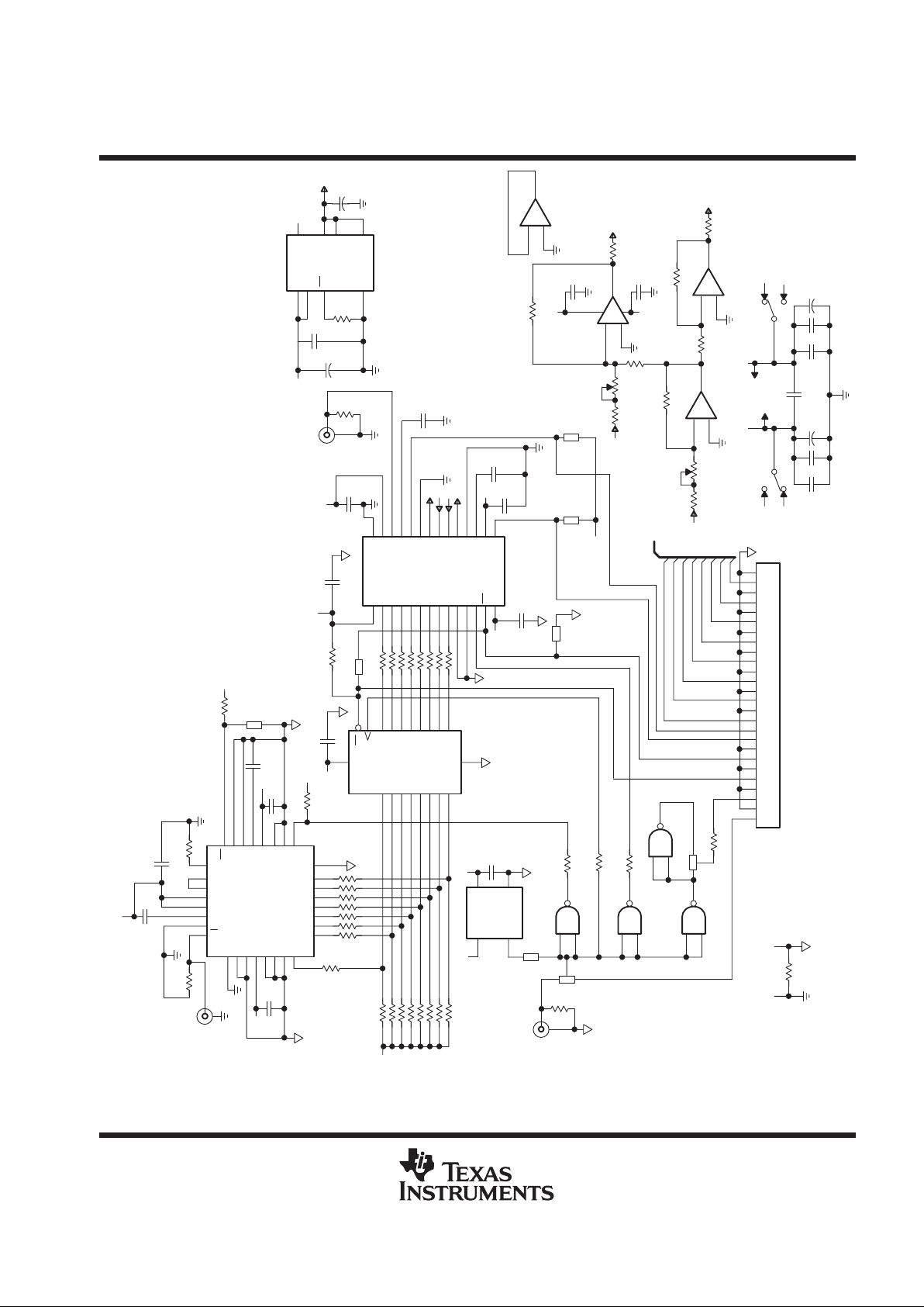
TLV5535 EV ALUATION MODULE
TLV5535 evaluation module
TI provides an evaluation module (EVM) for TL V5535. The EVM also includes a 10b 80 MSPS DAC so that the
user can convert the digitized signal back to the analog domain for functional testing. Performance
measurements can be done by capturing the ADC’s output data.
The EVM provides the following additional features:
D
Provision of footprint for the connection of an onboard crystal oscillator, instead of using an external clock
input.
D
Use of TLV5535 internal or external voltage references. In the case of external references, an onboard
circuit is used that derives adjustable bottom and top reference voltages from a bandgap reference. Two
potentiometers allow for the independent adjustments of both references. The full scale ADC range can be
adjusted to the input signal amplitude.
D
All digital output, control signal I/O (output enable, standby, reference powerdown) and clock I/O are
provided on a single connector. The EVM can thus be part of a larger (DSP) system for prototyping.
D
Onboard prototyping area with analog and digital supply and ground connections.
Figure 15 shows the EVM schematic.
The EVM is factory shipped for use in the following configuration:
D
Use of external (onboard) voltage references
D
External clock input
analog input
A signal in the range between V
(REFBI)
and V
(REFTI)
should be applied to avoid overflow/underflow on connector
J10. This signal is onboard terminated with 50Ω. There is no onboard biasing of the signal. When using external
(onboard) references, these levels can be adjusted with R7 (V
(REFTI)
) and R6 (V
(REFBI)
). Adjusting R7 causes
both references to shift. R6 only impacts the bottom reference. The range of these signals for which the device
is specified depends on AV
DD
and is shown in the
Recommended Operating Conditions
.
Internally generated reference levels are also dependent on AV
DD
as shown in the electrical characteristics
section.
clock input
A clock signal should be applied with amplitudes ranging from 0 to A VDD with a frequency equal to the desired
sampling frequency on connector J9. This signal is onboard terminated with 50 Ω. Both ADC and DAC run of f
the same clock signal. Alternatively the clock can be applied from terminal 1 on connector J11. A third option
is using a crystal oscillator. The EVM board provides the footprint for a crystal oscillator that can be populated
by the end-user, depending on the desired frequency. The footprint is compatible with the Epson EG-8002DC
series of programmable high-frequency crystal oscillators. Refer to the TLV5535 EVM Settings for selecting
between the different clock modes.

TLV5535
8-BIT, 35 MSPS, LOW-POWER ANALOG-TO-DIGITAL CONVERTER
SLAS221 – JUNE 1999
18
POST OFFICE BOX 655303 • DALLAS, TEXAS 75265
TLV5535 EV ALUATION MODULE
power supplies
The board provides seven power supply connectors (see T able 2). For optimum performance, analog and digital
supplies should be kept separate. Using separate supplies for the digital logic portion of TL V5535 (DVDD) and
its output drivers (DRVDD) benefits dynamic performance, especially when DRVDD is put at the minimum
required voltage (3 V), while DVDD might be higher (up to 3.6 V). This lowers the switching noise on the die
caused by the output drivers.
Table 2. Power Supplies
SIGNAL
NAME
CONNECTOR
BOARD
LABEL
DESCRIPTION
DRV3 J1 3DRV 3.3 V digital supply for TLV5535 (digital output drivers)
DV3 J2 3VD 3.3 V digital supply for TLV5535 (digital logic) and peripherals
DV5 J3 5VD 5 V digital supply for D/A converter and peripherals
AV3 J4 3VA 3.3 V analog supply for TLV5535
AV5 J5 5VA 5 V analog supply for onboard reference circuit and D/A converter. Can be left unconnected if
internal references are used and no D/A conversion is required.
AV+12 J6 12VA 12 V analog supply for onboard reference circuit. Can be left unconnected if internal references
are used.
AV–12 J7 –12VA –12 V analog supply for onboard reference circuit. Can be left unconnected if internal
references are used.
voltage references
SW1 and SW2 switch between internal and external top and bottom references respectively. The external
references are onboard generated from a stable bandgap-derived 3.3 V signal (using TI’s TPS7133 and
quad-opamp TLE2144). They can be adjusted via potentiometers R6 (V
(REFBI)
) and R7 (V
(REFTI)
). It is advised
to power down the internal voltage references by asserting PWN_REF when onboard references are used.
The references are measured at test points TP3 (V
(REFB)
) and TP4 (V
(REFT)
).
DAC output
The onboard DAC is a 10-bit 80 MSPS converter. It is connected back-to-back to the TLV5535. While the user
could use its analog output for measurements, the DAC output is directly connected to connector J8 and does
not pass through an analog reconstruction filter. So mirror spectra from aliased signal components feed through
into the analog output.
For this reason and to separate ADC and DAC contributions, performance measurements should be made by
capturing the ADC output data available on connector J11 and not by evaluating the DAC output.

TLV5535
8-BIT, 35 MSPS, LOW-POWER ANALOG-TO-DIGITAL CONVERTER
SLAS221 – JUNE 1999
19
POST OFFICE BOX 655303 • DALLAS, TEXAS 75265
TLV5535 EV ALUATION MODULE
TLV5535 EVM settings
clock input settings
REFERENCE
DESIGNATOR
FUNCTION
W1 Clock selection switch
1–2 J11: clock from pin1 on J11 connector
2–3 J9: clock from J9 SMA connector
W2 Clock source switch
J
XTL: clock from onboard crystal oscillator
j
CLK: clock from pin 1 on J11 connector (if W1/1–2) or J9 SMA connector (if W1/2–3)
NOTE: If set to XTL and a XTL oscillator is populated, no clock signal should be applied to J9 or J1 1, depending on the W1
setting.
W3 Clock output switch
1–2 Rising: clock output on J1 1 connector is the same phase as the clock to the digital output buffer . Data changes on rising
CLK edge.
2–3 Falling: clock output on J1 1 connector is the opposite phase as the digital output buffer. Data changes on falling CLK edge.
reference settings
REFERENCE
DESIGNATOR
FUNCTION
SW1 REFT external/internal switch
Jj
REFT internal: REFT from TLV5535 internal reference
jJ
REFT external: REFT from onboard voltage reference circuit
SW2 REFB external/internal switch
Jj
REFB internal: REFB from TLV5535 internal reference
jJ
REFB external: REFB from onboard voltage reference circuit
control settings
REFERENCE
DESIGNATOR
FUNCTION
W4 TL V5535 and digital output buf fer output enable control (1)
J
5535-574 OE
-connected: Connects OEs of TLV5535 and digital output buffer (574 buffer). Use this when no
board-external OE
is used. In addition, close W5 to have both OEs permanently enabled.
j
5535-574 OE
-disconnected: Disconnects OEs of TL V5535 and digital output buffer (574 buffer). The OE for the output
buffer needs to be pulled low from pin 5 on J1 1 connector to enable. The OE
for TLV5535 is independently controlled from
pin 7 on J11 connector (W5 open) or is permanently enabled if W5 is closed.
W5 TL V5535 and digital output buf fer output enable control (2)
J
5535 OE
to GND: Connects OEs of TLV5535 to GND. Additionally connects OE of 74ALS574 to GND if W4 is 5535-574
OE
-connected.
j
5535 OE
external: Enables control of OE of TL V5535 via pin 7 on J1 1 connector . When taken high (internal pulldown)
the output can be disabled.
W6 TL V5535 STDBY control
J
Stdby: STDBY is active (high).
j
Active: STDBY is low, via internal pulldown. STDBY can be taken high from pin 9 on J11 connector to enable standby
mode.

TLV5535
8-BIT, 35 MSPS, LOW-POWER ANALOG-TO-DIGITAL CONVERTER
SLAS221 – JUNE 1999
20
POST OFFICE BOX 655303 • DALLAS, TEXAS 75265
TLV5535 EV ALUATION MODULE
control settings (continued)
REFERENCE
DESIGNATOR
FUNCTION
W7 TL V5535 PWDN REF control
J
Pwdn_ref: PWDN_REF is active (high).
j
Active: PWDN_REF is low , via internal pulldown. PWDN_REF can be taken high from pin 10 on J11 connector to enable
pwdn_ref mode.
W8 DAC enable
J
Active: D/A on
j
Standby: D/A off
TLV5535
8-BIT, 35 MSPS, LOW-POWER ANALOG-TO-DIGITAL CONVERTER
SLAS221 – JUNE 1999
21
POST OFFICE BOX 655303 • DALLAS, TEXAS 75265
AVSSNCDVSS
DVDDNCD0D1D2
D3
D4
D5
D6
D7
D8
D9
NC
IO
CE
NC
DVSS
VB
DVDD
NC
BLK
CLK
IO
VG
AVDD
AVDD
VREF
SREF
IREF
25262728293031
32
1
2
3
4
5
6
7
8
11161514131210
9
C30
.1 µF
DV5
24
23
22
21
20
19
18
17
R3
200
C25
.1 µF
R4
3.24 kΩ
U3
C26
.1 µF
CXD2306Q
C29
.1 µF
DV5
C28
.1 µF
R11
10 kΩ
DV5
R14
10 kΩ
DV5
W8
R25
R23
R22
R21
R20
R19
R18
20
20
20
20
20
20
20
R24
20
10 kΩ
10 kΩ
10 kΩ
10 kΩ
10 kΩ
10 kΩ
10 kΩ
10 kΩ
R48
R47
R46
R45
R44
R43
R42
R41
DV5
19181716151413
12
1Q2Q3Q4Q5Q6Q7Q
8Q
DGND
DV3
20
10
1D2D3D4D5D6D7D
8D
OC
CLK
1
1123456789
U5
C41
.1 µF
DV3
SN74LVT574DW
20202020202020
20
R39
R38
R36
R35
R33
R32
R31
R30
C24
.1 µF
DV5DV5
OE
OUT
VCC
GND
W2
12
13
11
R13
20
J9
CLOCK IN
J8
DAC_OUT
AV5
R29
20
U2D
SN74ALVC00
9
10
8
R17
20
U2C
1
2
3
U2A
4
5
6
U2B
W3
R37
20
CLK_OUT
1
2
3
4
5
6
7
8
9
10
11
12
13
14
15
16
17
18
19
20
21
22
23
24
25
26
W1
321
R28
49.9
CLK_IN
Q(0–7)
Q7Q6Q5Q4Q3Q2Q1
Q0
W4
1
DRVDD
AVSS
28
2345678
9
1011121314
U6
D0D1D2D3D4D5D6D7DRVSS
DVSS
CLKOEDVDD
27262524232221201918171615
AVDD
AIN
CML
PWDN_REF
AVSS
REFBO
REFBI
REFTI
REFTO
AVSS
BG
AVDD
STDBY
R40
10 kΩ
DRV3
C45
.1 µF
C35
.1 µF
DV3
TLV5535PW
W5
W6
C33
.1 µF
C34
.1 µF
AV3
W7
DV3
C42
.1 µF
C46
.1 µF
AV3
J10
ANALOG IN
R34
49.9
C36
.01 µF
C39
.1 µF
+
C38
10µ F
C37
.01 µF
C43
.1 µF
+
C44
10µ F
SW2 SW1
REFBO
EXT_REFB EXT_REFT
REFTO
REFBI
REFTI
TP3 TP4
C40
.1 µF
3IN
3IN
–
+
3OUT
11
12
10
4IN
4IN
–
+
4OUT
15
14
16
U4C
U4D
1IN
1IIN
–
+
1OUT
2
3
1
U4A
R7
1 kΩ
R8
1 kΩ
REF3V
R9
1 kΩ
R12
1 kΩ
R16
1 kΩ
R27
10
EXT_REFT
R6 5 kΩ
R5
2.1 kΩ
REF3V
2IN
2IN
–
+
2OUT
6
5
7
U4B
C32
.1 µF
AV –12
C31
.1 µF
AV +12
R15
1 kΩ
EXT_REFB
R26
10
TLE2144CDW
ININEN
GND
PG
OUT
OUT
SENSE
R1
10 kΩ
342
1
8
6
5
7
+
C23
10µ F
C27
.1 µF
+
C22
10µ F
AV5
REF3V
TP1 TP2
R2
0
1 kΩ
R10
TLE2144CDW
J11
X1
4
13
U1
TPS7133QD
SN74ALVC00
SN74ALVC00
SN74ALVC00
Figure 15. EVM Schematic
TLV5535
8-BIT, 35 MSPS, LOW-POWER ANALOG-TO-DIGITAL CONVERTER
SLAS221 – JUNE 1999
22
POST OFFICE BOX 655303 • DALLAS, TEXAS 75265
TLV5535 EV ALUATION MODULE
+
+
C20
10 µF
C12
10 µF
C11
1 µF
L6
4.7 µH
1
2
J6
Analog +12 V
AV +12 V
C21
10 µF
C14
10 µF
C13
1 µF
L7
4.7 µH
1
2
J7
Analog –12 V
AV –12 V
+
+
+
+
C19
10 µF
C10
10 µF
C9
1 µF
L5
4.7 µH
1
2
J5
Analog +5 V
AV5
+
+
C18
10 µF
C8
10 µF
C7
1 µF
L4
4.7 µH
1
2
J4
Analog +3.3 V
AV3
+
+
C17
10 µF
C6
10 µF
C5
1 µF
L3
4.7 µH
1
2
J3
Digital +5 V
DV5
+
+
C16
10 µF
C4
10 µF
C3
1 µF
L2
4.7 µH
1
2
J2
Digital +3.3 V (DVDD)
DV3
+
+
C15
10 µF
C2
10 µF
C1
1 µF
L1
4.7 µH
1
2
J1
Digital +3.3 V (DRVDD)
DRV3
Figure 15. EVM Schematic (continued)

TLV5535
8-BIT, 35 MSPS, LOW-POWER ANALOG-TO-DIGITAL CONVERTER
SLAS221 – JUNE 1999
23
POST OFFICE BOX 655303 • DALLAS, TEXAS 75265
TLV5535 EV ALUATION MODULE
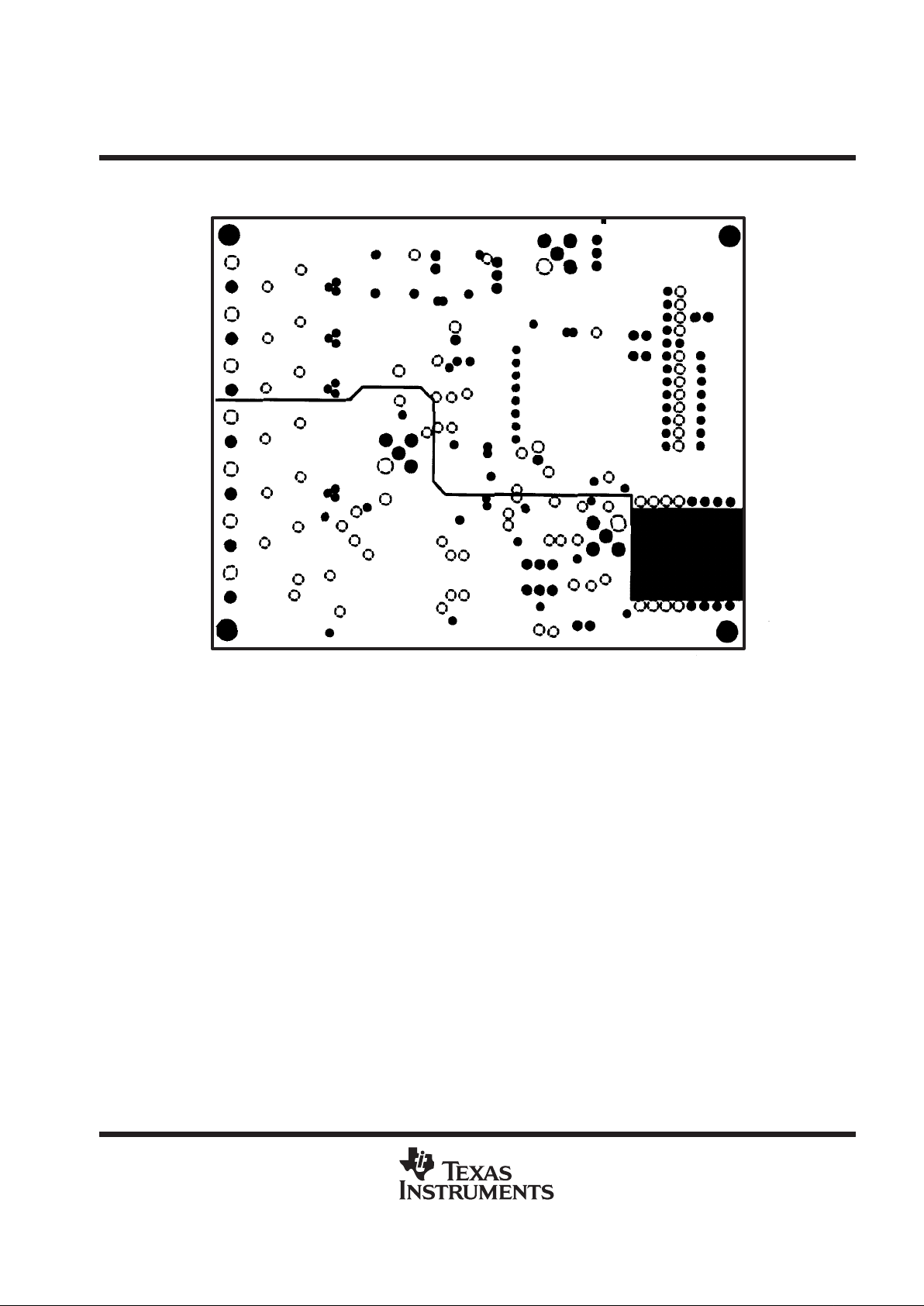
Figure 16. EVM Board Layout, Top Overlay

TLV5535
8-BIT, 35 MSPS, LOW-POWER ANALOG-TO-DIGITAL CONVERTER
SLAS221 – JUNE 1999
24
POST OFFICE BOX 655303 • DALLAS, TEXAS 75265
TLV5535 EV ALUATION MODULE
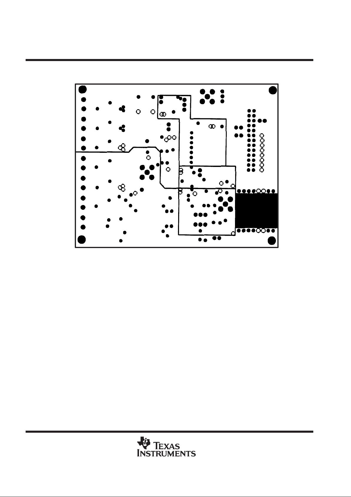
Figure 17. EVM Board Layout, Top Layer
TLV5535
8-BIT, 35 MSPS, LOW-POWER ANALOG-TO-DIGITAL CONVERTER
SLAS221 – JUNE 1999
25
POST OFFICE BOX 655303 • DALLAS, TEXAS 75265
TLV5535 EV ALUATION MODULE
Figure 18. EVM Board Layout, Internal Plane 1
TLV5535
8-BIT, 35 MSPS, LOW-POWER ANALOG-TO-DIGITAL CONVERTER
SLAS221 – JUNE 1999
26
POST OFFICE BOX 655303 • DALLAS, TEXAS 75265
TLV5535 EV ALUATION MODULE
Figure 19. EVM Board Layout, Internal Plane 2

TLV5535
8-BIT, 35 MSPS, LOW-POWER ANALOG-TO-DIGITAL CONVERTER
SLAS221 – JUNE 1999
27
POST OFFICE BOX 655303 • DALLAS, TEXAS 75265
TLV5535 EV ALUATION MODULE
3350 (mil)
4200 (mil)
Figure 20. EVM Board Layout, Drill Drawing for Through Hole

TLV5535
8-BIT, 35 MSPS, LOW-POWER ANALOG-TO-DIGITAL CONVERTER
SLAS221 – JUNE 1999
28
POST OFFICE BOX 655303 • DALLAS, TEXAS 75265
TLV5535 EV ALUATION MODULE
Figure 21. EVM Board Layout, Bottom Layer

TLV5535
8-BIT, 35 MSPS, LOW-POWER ANALOG-TO-DIGITAL CONVERTER
SLAS221 – JUNE 1999
29
POST OFFICE BOX 655303 • DALLAS, TEXAS 75265
TLV5535 EV ALUATION MODULE
T able 3. TLV5535EVM Bill of Material
QTY. REFERENCE DESIGNATOR VALUE SIZE DESCRIPTION
MANUFACTURER/
PART NUMBER
†
7 C1, C11, C13, C3, C5, C7, C9 1 µF 1206 ceramic multilayer capacitor Any
18 C10, C12, C14, C15, C16,
C17, C18, C19, C2, C20, C21,
C22, C23, C4, C6, C8, C38,
C44
10 µF 3216 16 V , 10 µF, tantalum capacitor Any
2 C36, C43 0.01 µF 805 Ceramic multilayer Any
19 C24, C25, C26, C27, C28,
C29, C30, C31, C32, C33,
C34, C35, C37, C39, C40,
C41, C42, C45, C46
0.1 µF 805 Ceramic multilayer capacitor Any
7 J1, J2, J3, J4, J5, J6, J7 Screw Con 2 terminal screw connector Lumberg
KRMZ2
3 J10, J8, J9 SMA PCM mount, SMA Jack Johnson Components
142-0701-206
1 J11 IDC26 13I × 2.025I square pin header Samtec
TSW-113-07-L-D
7 L1, L2, L3, L4, L5, L6, L7 4.7 µH 4.7 µH DO1608C-472-Coil Craft Coil Craft
DO1608-472
1 R2 0 1206 Chip resistor Any
2 R26, R27 10 1206 Chip resistor Any
12 R1, R11, R14, R40, R41, R42,
R43, R44, R45, R46, R47, R48
10 K 1206 Chip resistor Any
6 R10, R12, R15, R16, R8, R9 1 K 1206 Chip resistor Any
1 R5 2.1 K 1206 Chip resistor Any
20 R13, R17, R18, R19, R20,
R21, R22, R23, R24, R25,
R29, R30, R31, R32, R33,
R35, R36, R37, R38, R39
20 1206 Chip resistor Any
1 R3 200 1206 Chip resistor Any
1 R4 3.24 K 1206 Chip resistor Any
2 R28, R34 49.9 1206 Chip resistor Any
1 R6 5 K 4 mm SM pot-top adjust Bourns
3214W-5K
1 R7 1 K 4 mm SM pot-top adjust Bourns
3214W-1K
2 SW1, SW2 SPDT C&K tiny series–slide switch C&K
TS01CLE
4 TP1, TP2, TP3, TP4 TP Test point, single 0.025I pin Samtec
TSW-101-07-L-S
or equivalent
1 U3 CXD2306Q Sony
CXD2306Q
1 U2 SN74ALVC00D 14-SOIC (D) Quad 2-input positive NAND Texas Instruments
SN74ALVC00D
1 U5 SN74LVT574DW 20-SOP (DW) Texas Instruments
SN74LVT574DW
†
Manufacturer and part number data for reference only. Equivalent parts might be substituted on the EVM.

TLV5535
8-BIT, 35 MSPS, LOW-POWER ANALOG-TO-DIGITAL CONVERTER
SLAS221 – JUNE 1999
30
POST OFFICE BOX 655303 • DALLAS, TEXAS 75265
TLV5535 EV ALUATION MODULE
Table 3. TLV5535EVM Bill of Material (Continued)
QTY. REFERENCE DESIGNATOR VALUE SIZE DESCRIPTION
MANUFACTURER/
PART NUMBER
†
1 U4 TLE2144CDW 16-SOP(D) Quad op amp Texas Instruments
TLE2144CDW/
TLE2144IDW
1 U6 TLV5535PW 28-TSSOP (PW) Texas Instruments
TLV5535PW
1 U1 TPS7133 8-SOP(D) Low-dropout voltage regulator Texas Instruments
TPS7133QD
6 W2, W4, W5, W6, W7, W8 SPST 2 position jumper , 0.1I spacing Samtec
TSW-102-07-L-S
or equivalent
2 W1, W3 DPFT 3 position jumper, 0.1I spacing Samtec
TSW-103-07-L-S
or equivalent
1 X1 NA Crystal oscillator Epson
SG-8002DC series
†
Manufacturer and part number data for reference only. Equivalent parts might be substituted on the EVM.

TLV5535
8-BIT, 35 MSPS, LOW-POWER ANALOG-TO-DIGITAL CONVERTER
SLAS221 – JUNE 1999
31
POST OFFICE BOX 655303 • DALLAS, TEXAS 75265
MECHANICAL DATA
PW (R-PDSO-G**) PLASTIC SMALL-OUTLINE PACKAGE
4040064/E 08/96
14 PIN SHOWN
Seating Plane
1,20 MAX
1
A
7
14
0,19
4,50
4,30
8
6,20
6,60
0,30
0,75
0,50
0,25
Gage Plane
0,15 NOM
0,65
M
0,10
0°–8°
0,10
PINS **
A MIN
A MAX
DIM
2,90
3,10
8
4,90
5,10
14
6,60
6,404,90
5,10
16
7,70
20
7,90
24
9,60
9,80
28
0,15
0,05
NOTES: A. All linear dimensions are in millimeters.
B. This drawing is subject to change without notice.
C. Body dimensions do not include mold flash or protrusion not to exceed 0,15.
D. Falls within JEDEC MO-153

IMPORTANT NOTICE
T exas Instruments and its subsidiaries (TI) reserve the right to make changes to their products or to discontinue
any product or service without notice, and advise customers to obtain the latest version of relevant information
to verify, before placing orders, that information being relied on is current and complete. All products are sold
subject to the terms and conditions of sale supplied at the time of order acknowledgment, including those
pertaining to warranty, patent infringement, and limitation of liability.
TI warrants performance of its semiconductor products to the specifications applicable at the time of sale in
accordance with TI’s standard warranty. Testing and other quality control techniques are utilized to the extent
TI deems necessary to support this warranty. Specific testing of all parameters of each device is not necessarily
performed, except those mandated by government requirements.
Customers are responsible for their applications using TI components.
In order to minimize risks associated with the customer’s applications, adequate design and operating
safeguards must be provided by the customer to minimize inherent or procedural hazards.
TI assumes no liability for applications assistance or customer product design. TI does not warrant or represent
that any license, either express or implied, is granted under any patent right, copyright, mask work right, or other
intellectual property right of TI covering or relating to any combination, machine, or process in which such
semiconductor products or services might be or are used. TI’s publication of information regarding any third
party’s products or services does not constitute TI’s approval, warranty or endorsement thereof.
Copyright 2000, Texas Instruments Incorporated
 Loading...