TLV5510
2.7-V TO 3.6-V 8-BIT HIGH-SPEED ANALOG-TO-DIGITAL CONVERTER
SLAS124C– DECEMBER 1997 – REVISED DECEMBER 1999
1
POST OFFICE BOX 655303 • DALLAS, TEXAS 75265
D
8-Bit Resolution
D
Integral Linearity Error
±0.75 LSB Max (25°C)
±1 LSB Max (–35°C to 85°C)
D
Differential Linearity Error
± 0.5 LSB (25°C)
±0.75 LSB Max (–35°C to 85°C)
D
Maximum Conversion Rate
10 Mega-Samples per Second
(MSPS) Min
D
2.7-V to 3.6-V Single-Supply Operation
D
Low Power Consumption ... 42 mW Typ at
3 V
D
Low Voltage Replacement for CXD1175
Applications
D
Communications
D
Digital Imaging
D
Video Conferencing
D
High-Speed Data Conversion
description
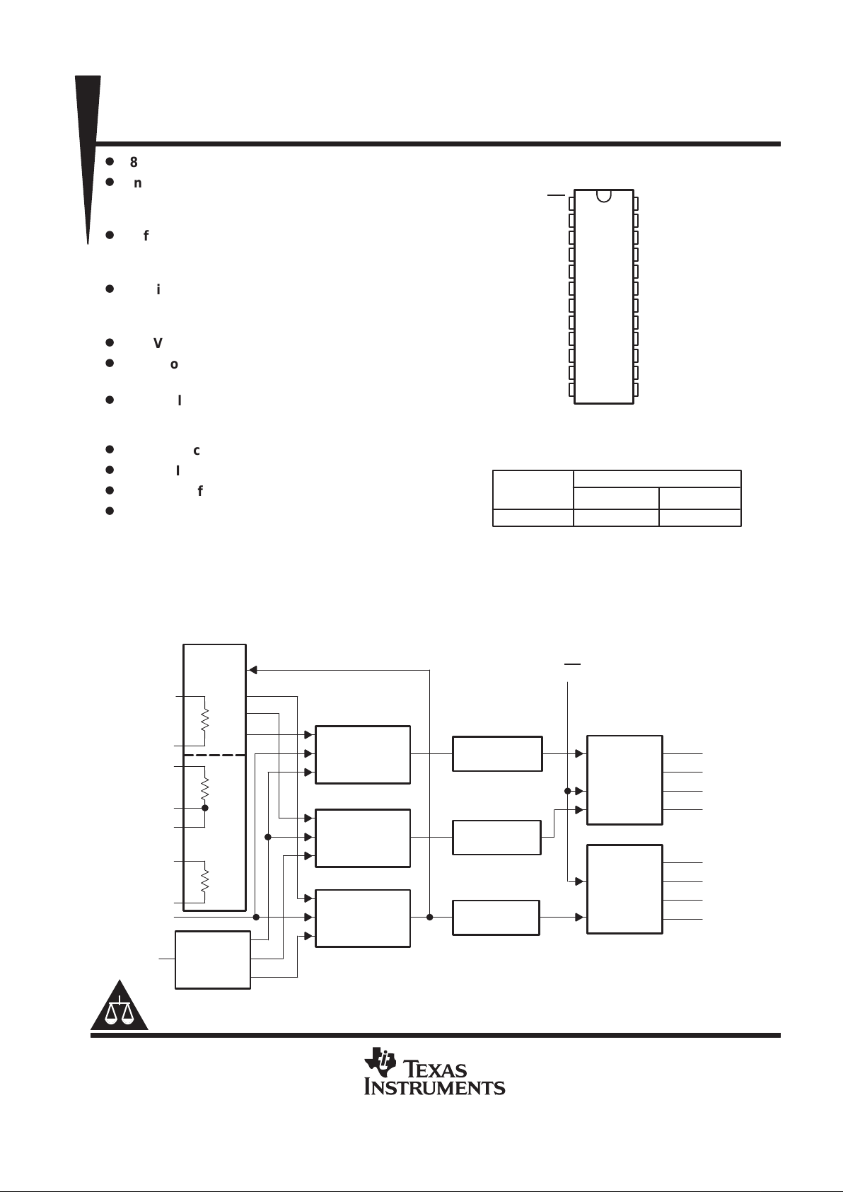
The TLV5510 is a CMOS 8-bit resolution semiflash analog-to-digital converter (ADC) with a 2.7-V to 3.6-V single
power supply and an internal reference voltage source. It converts a wide band analog signal (such as a video
signal) to a digital signal at a sampling rate of dc to 10 MHz.
functional block diagram
Lower Sampling
Comparators
(4 Bit)
Lower Encoder
(4 Bit)
Lower Data
Latch
Lower Sampling
Comparators
(4 Bit)
Lower Encoder
(4 Bit)
Upper Sampling
Comparators
(4 Bit)
Upper Encoder
(4 Bit)
Upper Data
Latch
Clock
Generator
OE
D1(LSB)
D2
D3
D4
D5
D6
D7
D8(MSB)
CLK
REFB
REFT
REFBS
AGND
AGND
ANALOG IN
V
DDA
REFTS
200 Ω
NOM
60 Ω
NOM
40 Ω
NOM
Resistor
Reference
Divider
Copyright 1999, Texas Instruments Incorporated
Please be aware that an important notice concerning availability, standard warranty, and use in critical applications of
Texas Instruments semiconductor products and disclaimers thereto appears at the end of this data sheet.
PRODUCTION DATA information is current as of publication date.
Products conform to specifications per the terms of Texas Instruments
standard warranty. Production processing does not necessarily include
testing of all parameters.
1
2
3
4
5
6
7
8
9
10
11
12
24
23
22
21
20
19
18
17
16
15
14
13
OE
DGND
D1(LSB)
D2
D3
D4
D5
D6
D7
D8(MSB)
V
DDD
CLK
DGND
REFB
REFBS
AGND
AGND
ANALOG IN
V
DDA
REFT
REFTS
V
DDA
V
DDA
V
DDD
PW OR NS PACKAGE
†
(TOP VIEW)
†
Also available in tape and reel and
ordered as the TL V5510INSR.
AVAILABLE OPTIONS
–35°C to 85°C
SOP (NS)
T
A
TLV5510INS
PACKAGE
TSSOP (PW)
TLV5510IPW
TLV5510
2.7-V TO 3.6-V 8-BIT HIGH-SPEED ANALOG-TO-DIGITAL CONVERTER
SLAS124C– DECEMBER 1997 – REVISED DECEMBER 1999
2
POST OFFICE BOX 655303 • DALLAS, TEXAS 75265
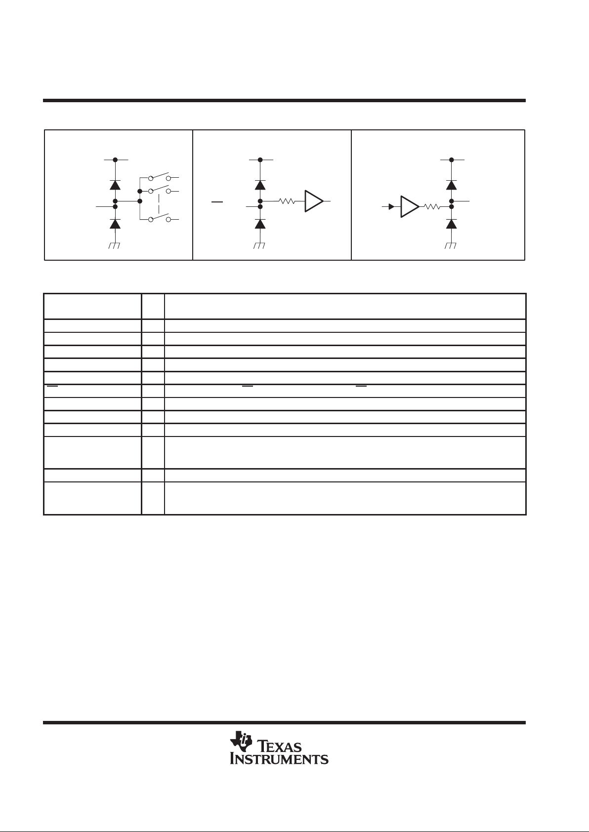
schematics of inputs and outputs
EQUIVALENT OF ANALOG INPUT
V
DDA
AGND
ANALOG IN
EQUIVALENT OF EACH DIGITAL INPUT
V
DDD
DGND
OE, CLK
EQUIVALENT OF EACH DIGITAL OUTPUT
V
DDD
DGND
D1–D8
Terminal Functions
TERMINAL
NAME NO.
I/O
DESCRIPTION
AGND 20, 21 Analog ground
ANALOG IN 19 I Analog input
CLK 12 I Clock input
DGND 2, 24 Digital ground
D1–D8 3–10 O Digital data out. D1:LSB, D8:MSB
OE 1 I Output enable. When OE = low, data is enabled. When OE = high, D1 – D8 is high impedance.
V
DDA
14, 15, 18 Analog supply voltage
V
DDD
11, 13 Digital supply voltage
REFB 23 I Reference voltage in (bottom)
REFBS 22 Reference voltage (bottom). When using the internal voltage divider to generate a nominal 2-V reference,
this terminal is shorted to the REFB terminal and the REFTS terminal is shorted to the REFT terminal (see
Figure 21).
REFT 17 I Reference voltage in (top)
REFTS 16 Reference voltage (top). When using the internal voltage divider to generate a nominal 2-V reference, this
terminal is shorted to the REFT terminal and the REFBS terminal is shorted to the REFB terminal (see
Figure 21).
absolute maximum ratings over operating free-air temperature range (unless otherwise noted)
†
Supply voltage, V
DDA
, V
DDD
7 V. . . . . . . . . . . . . . . . . . . . . . . . . . . . . . . . . . . . . . . . . . . . . . . . . . . . . . . . . . . . . . . . .
Reference voltage input range, REFT, REFB, REFBS, REFTS AGND to V
DDA
. . . . . . . . . . . . . . . . . . . . . . . . .
Analog input voltage range, V
I(ANLG)
AGND to V
DDA
. . . . . . . . . . . . . . . . . . . . . . . . . . . . . . . . . . . . . . . . . . . . . . .
Digital input voltage range, V
I(DGTL)
DGND to V
DDD
. . . . . . . . . . . . . . . . . . . . . . . . . . . . . . . . . . . . . . . . . . . . . . . .
Digital output voltage range, V
O(DGTL)
DGND to V
DDD
. . . . . . . . . . . . . . . . . . . . . . . . . . . . . . . . . . . . . . . . . . . . .
Operating free-air temperature range, T
A
–35°C to 85°C. . . . . . . . . . . . . . . . . . . . . . . . . . . . . . . . . . . . . . . . . . . .
Storage temperature range, T
stg
–55°C to 150°C. . . . . . . . . . . . . . . . . . . . . . . . . . . . . . . . . . . . . . . . . . . . . . . . . . .
†
Stresses beyond those listed under “absolute maximum ratings” may cause permanent damage to the device. These are stress ratings only, and
functional operation of the device at these or any other conditions beyond those indicated under “recommended operating conditions” is not
implied. Exposure to absolute-maximum-rated conditions for extended periods may affect device reliability.
TLV5510
2.7-V TO 3.6-V 8-BIT HIGH-SPEED ANALOG-TO-DIGITAL CONVERTER
SLAS124C– DECEMBER 1997 – REVISED DECEMBER 1999
3
POST OFFICE BOX 655303 • DALLAS, TEXAS 75265
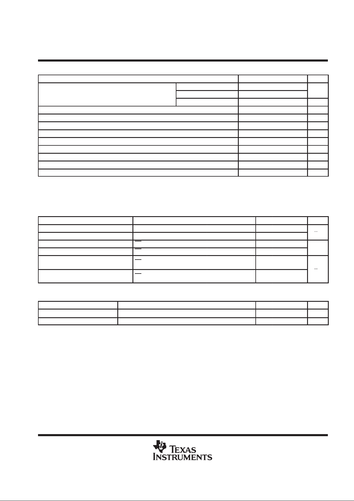
recommended operating conditions
MIN NOM MAX UNIT
V
DDA
–AGND 2.7 3 3.6
Supply voltage
V
DDD
–DGND 2.7 3 3.6
V
AGND–DGND –100 0 100 mV
Reference input voltage (top), REFT REFB+2 VDDA–0.3 V
Reference input voltage (bottom), REFB 0 0.6 REFT–2 V
Analog input voltage range, V
I(ANLG)
(see Note 1)
REFB
REFT V
High-level input voltage, V
IH
2.5 V
Low-level input voltage, V
IL
0.5 V
Pulse duration, clock high, t
w(H)
10 ns
Pulse duration, clock low, t
w(L)
10 ns
Clock frequency, f
(CLK)
10 MHz
Sampling frequency, f
s
10 MSPS
NOTE 1: REFT – REFB ≤ 2.4 V maximum
electrical characteristics at V
DDD
= V
DDA
= 3 V, REFT = 2.5 V, REFB = 0.5 V, f
(CLK)
= 10 MHz,
T
A
= 25°C (unless otherwise noted)
digital I/O
PARAMETER TEST CONDITIONS
†
MIN TYP MAX UNIT
I
IH
High-level input current V
DDD
= MAX, VIH = V
DDD
5
I
IL
Low-level input current V
DDD
= MAX, VIL = 0 5
µ
A
I
OH
High-level output current OE = GND, V
DDD
= MIN, VOH = V
DDD
–0.5 V –1.6
I
OL
Low-level output current OE = GND, V
DDD
= MIN, VOL = 0.4 V 2.6
mA
I
OZH
High-level high-impedance-state
output leakage current
OE = V
DDD
, V
DDD
= MAX VOH = V
DDD
15
I
OZL
Low-level high-impedance-state
output leakage current
OE = V
DDD
, V
DDD
= MIN VOL = 0 15
µ
A
†
Conditions marked MIN or MAX are as stated in recommended operating conditions.
power
PARAMETER TEST CONDITIONS
†
MIN TYP MAX UNIT
I
DD
Supply current f
sin
= 1 MHz sine wave, reference resistor dissipation is separate 4 10 mA
I
ref
Reference voltage current ∆REF = REFT – REFB = 2 V 6 10 14 mA
†
Conditions marked MIN or MAX are as stated in recommended operating conditions.
TLV5510
2.7-V TO 3.6-V 8-BIT HIGH-SPEED ANALOG-TO-DIGITAL CONVERTER
SLAS124C– DECEMBER 1997 – REVISED DECEMBER 1999
4
POST OFFICE BOX 655303 • DALLAS, TEXAS 75265
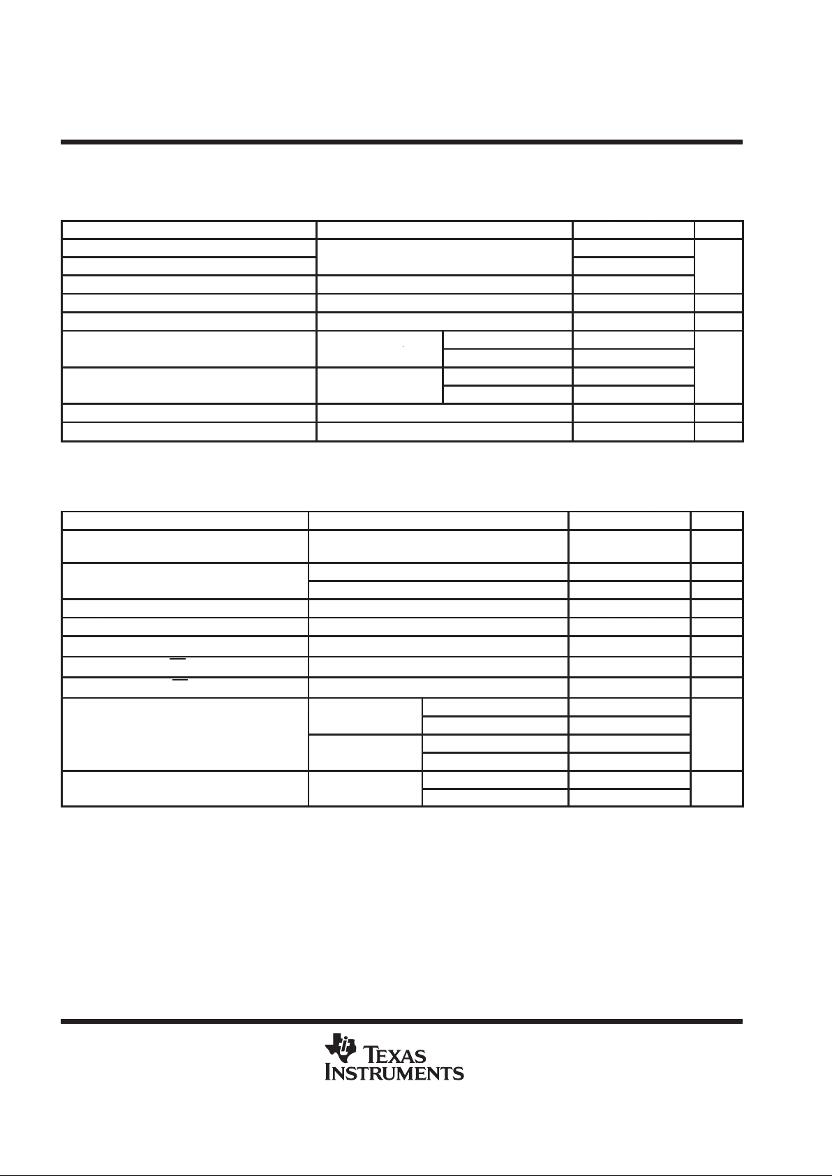
electrical characteristics at V
DDD
= V
DDA
= 3 V, REFT = 2.5 V, REFB = 0.5 V, f
(CLK)
= 10 MHz,
T
A
= 25°C (unless otherwise noted) (continued)
static performance
PARAMETER TEST CONDITIONS
†
MIN TYP MAX UNIT
Self-bias (1), at REFB
0.54 0.60 0.72
Self-bias (1), REFT – REFB
Short REFB to REFBS
,
Short REFT to REFTS
1.8 2 2.4
V
Self-bias (2), at REFT Short REFB to AGND, Short REFT to REFTS 2.25 2.5 3
R
ref
Reference voltage resistor Between REFT and REFB 140 200 260 Ω
C
i
Analog input capacitance V
I(ANLG)
= 1.5 V + 0.07 V
rms
16 pF
f
= 10 MHz,
TA = 25°C ±0.3 ±0.75
Integral nonlinearity (INL)
(CLK)
,
VI = 0.5 V to 2.5 V
TA = –35°C to 85°C ±1
f
= 10 MHz,
TA = 25°C ±0.2 ±0.5
LSB
Differential nonlinearity (DNL)
(CLK)
,
VI = 0.5 V to 2.5 V
TA = –35°C to 85°C ±0.75
E
ZS
Zero-scale error ∆REF = REFT – REFB = 2 V –18 –43 –68 mV
E
FS
Full-scale error ∆REF = REFT – REFB = 2 V –20 0 20 mV
†
Conditions marked MIN or MAX are as stated in recommended operating conditions.
operating characteristics at V
DDD
= V
DDA
= 3 V, REFT = 2.5 V, REFB = 0.5 V, f
(CLK)
= 10 MHz,
T
A
= 25°C (unless otherwise noted)
PARAMETER TEST CONDITIONS MIN TYP MAX UNIT
f
conv
Maximum conversion rate
fI = 1-kHz ramp wave form,
V
I(ANLG)
= 0.5 V – 2.5 V
0.2 10 MSPS
p
At – 1 dB 17 MHz
BW
Analog input bandwidth
At – 3 dB 36 MHz
t
d(D)
Digital output delay time CL ≤ 10 pF (see Note 1 and Figure 1) 18 30 ns
t
AJ
Aperture jitter time 30 ps
t
d(s)
Sampling delay time 4 ns
t
en
Enable time, OE↓ to valid data CL = 10 pF 15 ns
t
dis
Disable time, OE↑ to high impedance CL = 10 pF 10 ns
p
TA = 25°C 41
p
Input tone
= 1 MHz
Full range 41
Spurious free dynamic range (SFDR)
p
TA = 25°C 38
dB
Input tone
= 1.4 MHz
Full range 38
p
TA = 25°C 38
SNR
Signal-to-noise ratio
Input tone
= 1.4 MHz
Full range 37
dB
NOTE 2: CL includes probe and jig capacitance.
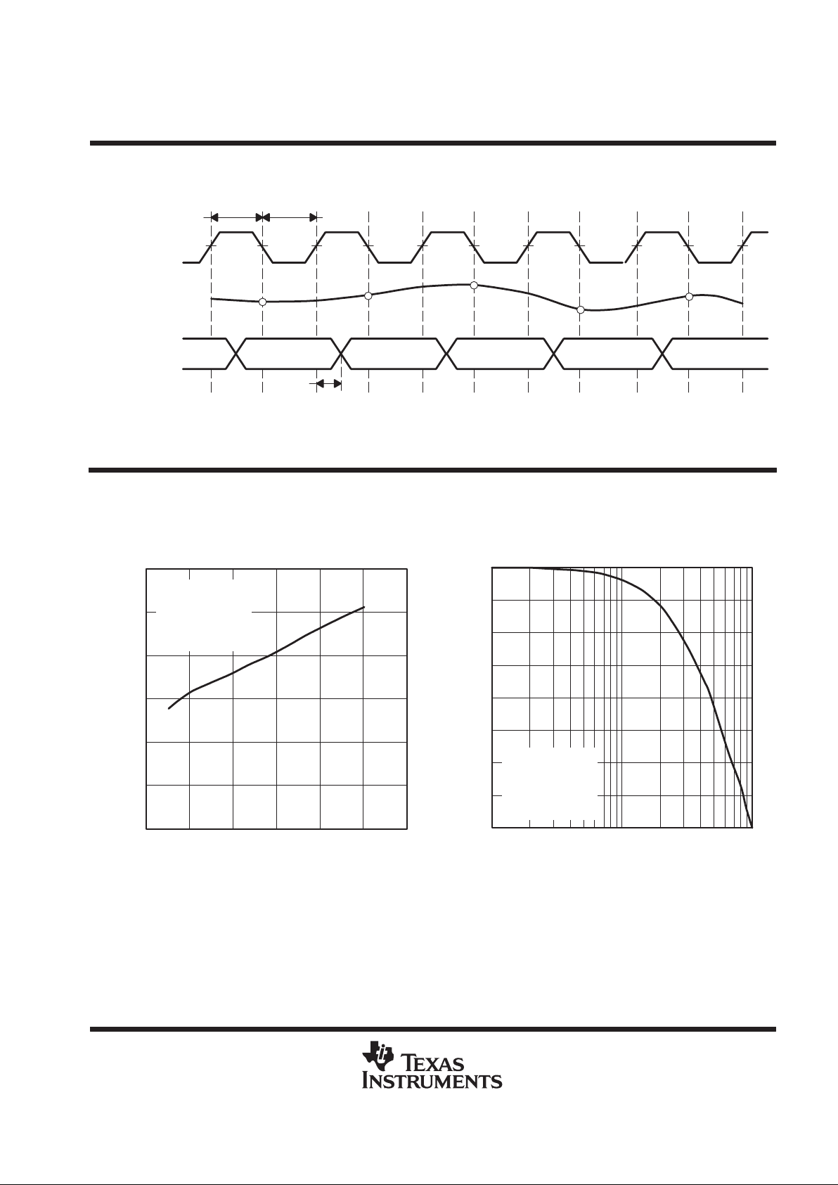
TLV5510
2.7-V TO 3.6-V 8-BIT HIGH-SPEED ANALOG-TO-DIGITAL CONVERTER
SLAS124C– DECEMBER 1997 – REVISED DECEMBER 1999
5
POST OFFICE BOX 655303 • DALLAS, TEXAS 75265
PARAMETER MEASUREMENT INFORMATION
N
N+1
N+2
N+3
N+4
N–3 N–2 N–1 N N+1
t
pd
CLK (Clock)
ANALOG IN
(Input Signal)
D1–D8
(Output Data)
t
w(H)
t
w(L)
Figure 1. I/O Timing Diagram
TYPICAL CHARACTERISTICS
Figure 2
6
4
2
0
02 4 6
Power Dissipation – mW
8
10
Sampling Frequency – MHz
POWER DISSIPATION
vs
SAMPLING FREQUENCY
12
81012
TA = 25°C
V
DDA
= 2.7 V,
V
REFB
= 0.5 V,
V
REFT
= 2.5 V,
Fclk = 10 MHz
Figure 3
10
0
–4
–5
–7
–8
–2
–1
0
Gain – dB
ANALOG INPUT BANDWIDTH
fI – Input Frequency – MHz
–3
–6
10
1
10
2
TA = 25°C
V
DDA
= 2.7 V,
V
REFB
= 0.5 V,
V
REFT
= 2.5 V,
Fclk = 10 MHz
TLV5510
2.7-V TO 3.6-V 8-BIT HIGH-SPEED ANALOG-TO-DIGITAL CONVERTER
SLAS124C– DECEMBER 1997 – REVISED DECEMBER 1999
6
POST OFFICE BOX 655303 • DALLAS, TEXAS 75265
TYPICAL CHARACTERISTICS
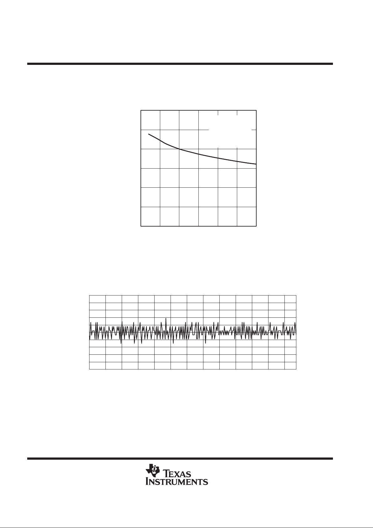
Figure 4
30
20
10
0
0 0.5 1 1.5
Signal-To-Noise Ratio – dB
40
50
Input Frequency – MHz
SIGNAL-TO-NOISE RATIO
vs
INPUT FREQUENCY
60
2 2.5 3
TA = 25°C
V
DDA
= 3 V,
V
REFB
= 0.5 V,
V
REFT
= 2.5 V,
Fclk = 10 MHz
0.2
–0.2
–0.3
–0.4
0 20 40 60 80 100 120
DNL – Differential Nonlinearity – LSB
0.3
0.4
Samples
0.5
140 160 180 200
0.1
0
–0.1
–0.5
220 240 253
DIFFERENTIAL NONLINEARITY
vs
SAMPLES
(Under Recommended Operating Conditions)
Figure 5
 Loading...