

TLV5510
2.7-V TO 3.6-V 8-BIT HIGH-SPEED ANALOG-TO-DIGITAL CONVERTER
SLAS124C– DECEMBER 1997 – REVISED DECEMBER 1999
1
POST OFFICE BOX 655303 • DALLAS, TEXAS 75265
D
8-Bit Resolution
D
Integral Linearity Error
±0.75 LSB Max (25°C)
±1 LSB Max (–35°C to 85°C)
D
Differential Linearity Error
± 0.5 LSB (25°C)
±0.75 LSB Max (–35°C to 85°C)
D
Maximum Conversion Rate
10 Mega-Samples per Second
(MSPS) Min
D
2.7-V to 3.6-V Single-Supply Operation
D
Low Power Consumption ... 42 mW Typ at
3 V
D
Low Voltage Replacement for CXD1175
Applications
D
Communications
D
Digital Imaging
D
Video Conferencing
D
High-Speed Data Conversion
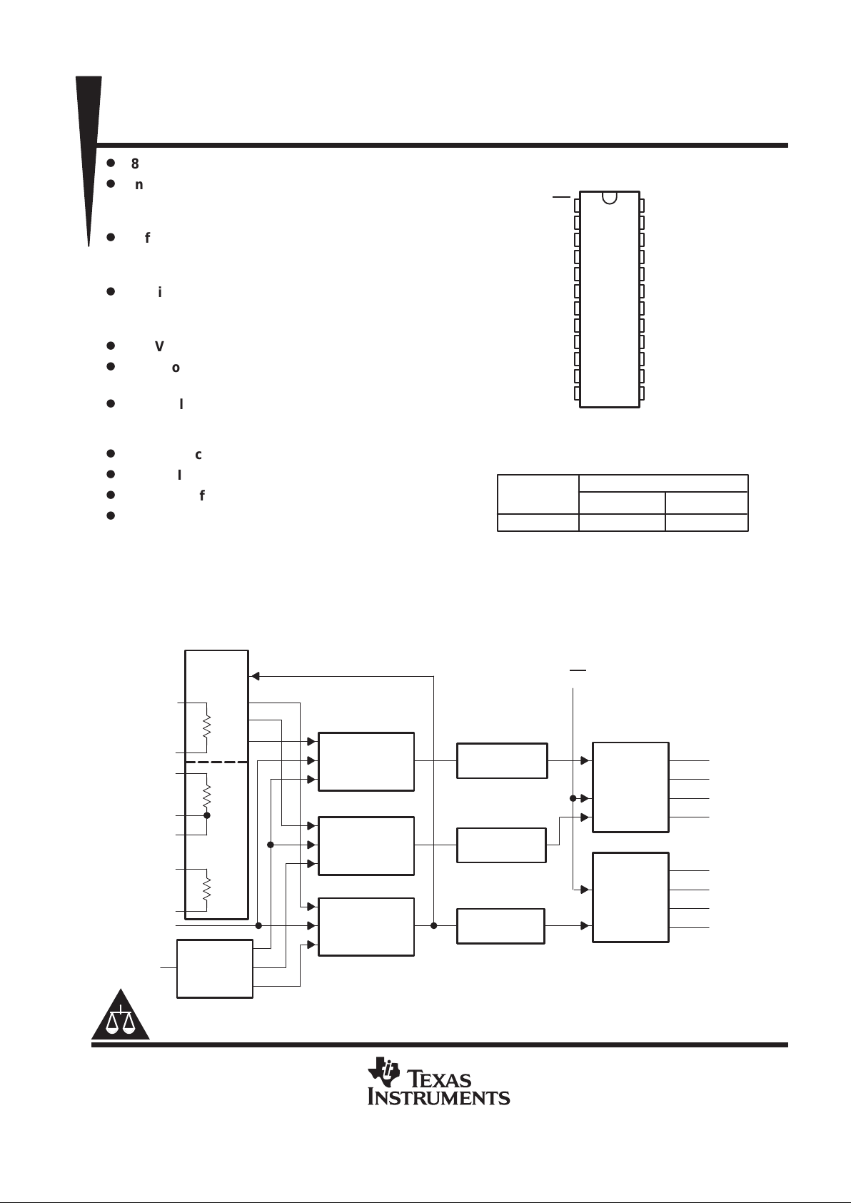
description
The TLV5510 is a CMOS 8-bit resolution semiflash analog-to-digital converter (ADC) with a 2.7-V to 3.6-V single
power supply and an internal reference voltage source. It converts a wide band analog signal (such as a video
signal) to a digital signal at a sampling rate of dc to 10 MHz.
functional block diagram
Lower Sampling
Comparators
(4 Bit)
Lower Encoder
(4 Bit)
Lower Data
Latch
Lower Sampling
Comparators
(4 Bit)
Lower Encoder
(4 Bit)
Upper Sampling
Comparators
(4 Bit)
Upper Encoder
(4 Bit)
Upper Data
Latch
Clock
Generator
OE
D1(LSB)
D2
D3
D4
D5
D6
D7
D8(MSB)
CLK
REFB
REFT
REFBS
AGND
AGND
ANALOG IN
V
DDA
REFTS
200 Ω
NOM
60 Ω
NOM
40 Ω
NOM
Resistor
Reference
Divider
Copyright 1999, Texas Instruments Incorporated
Please be aware that an important notice concerning availability, standard warranty, and use in critical applications of
Texas Instruments semiconductor products and disclaimers thereto appears at the end of this data sheet.
PRODUCTION DATA information is current as of publication date.
Products conform to specifications per the terms of Texas Instruments
standard warranty. Production processing does not necessarily include
testing of all parameters.
1
2
3
4
5
6
7
8
9
10
11
12
24
23
22
21
20
19
18
17
16
15
14
13
OE
DGND
D1(LSB)
D2
D3
D4
D5
D6
D7
D8(MSB)
V
DDD
CLK
DGND
REFB
REFBS
AGND
AGND
ANALOG IN
V
DDA
REFT
REFTS
V
DDA
V
DDA
V
DDD
PW OR NS PACKAGE
†
(TOP VIEW)
†
Also available in tape and reel and
ordered as the TL V5510INSR.
AVAILABLE OPTIONS
–35°C to 85°C
SOP (NS)
T
A
TLV5510INS
PACKAGE
TSSOP (PW)
TLV5510IPW
TLV5510
2.7-V TO 3.6-V 8-BIT HIGH-SPEED ANALOG-TO-DIGITAL CONVERTER
SLAS124C– DECEMBER 1997 – REVISED DECEMBER 1999
2
POST OFFICE BOX 655303 • DALLAS, TEXAS 75265
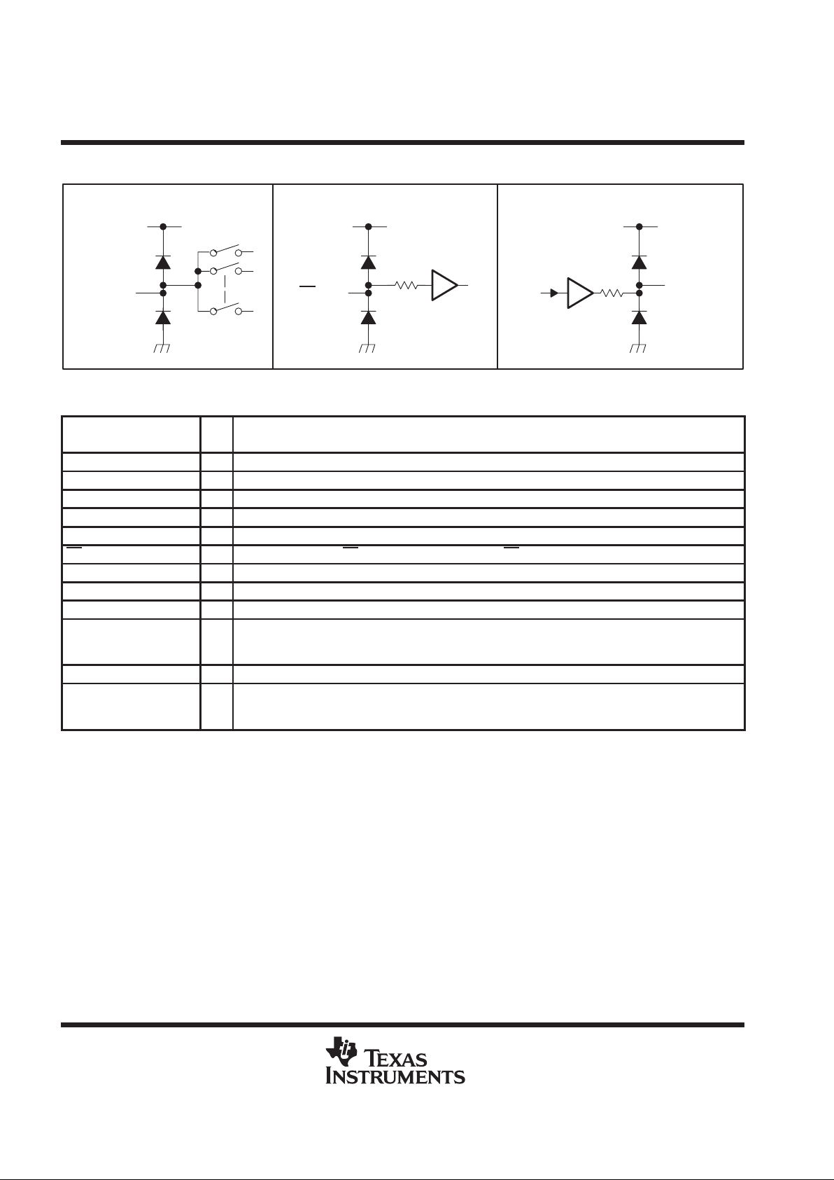
schematics of inputs and outputs
EQUIVALENT OF ANALOG INPUT
V
DDA
AGND
ANALOG IN
EQUIVALENT OF EACH DIGITAL INPUT
V
DDD
DGND
OE, CLK
EQUIVALENT OF EACH DIGITAL OUTPUT
V
DDD
DGND
D1–D8
Terminal Functions
TERMINAL
NAME NO.
I/O
DESCRIPTION
AGND 20, 21 Analog ground
ANALOG IN 19 I Analog input
CLK 12 I Clock input
DGND 2, 24 Digital ground
D1–D8 3–10 O Digital data out. D1:LSB, D8:MSB
OE 1 I Output enable. When OE = low, data is enabled. When OE = high, D1 – D8 is high impedance.
V
DDA
14, 15, 18 Analog supply voltage
V
DDD
11, 13 Digital supply voltage
REFB 23 I Reference voltage in (bottom)
REFBS 22 Reference voltage (bottom). When using the internal voltage divider to generate a nominal 2-V reference,
this terminal is shorted to the REFB terminal and the REFTS terminal is shorted to the REFT terminal (see
Figure 21).
REFT 17 I Reference voltage in (top)
REFTS 16 Reference voltage (top). When using the internal voltage divider to generate a nominal 2-V reference, this
terminal is shorted to the REFT terminal and the REFBS terminal is shorted to the REFB terminal (see
Figure 21).
absolute maximum ratings over operating free-air temperature range (unless otherwise noted)
†
Supply voltage, V
DDA
, V
DDD
7 V. . . . . . . . . . . . . . . . . . . . . . . . . . . . . . . . . . . . . . . . . . . . . . . . . . . . . . . . . . . . . . . . .
Reference voltage input range, REFT, REFB, REFBS, REFTS AGND to V
DDA
. . . . . . . . . . . . . . . . . . . . . . . . .
Analog input voltage range, V
I(ANLG)
AGND to V
DDA
. . . . . . . . . . . . . . . . . . . . . . . . . . . . . . . . . . . . . . . . . . . . . . .
Digital input voltage range, V
I(DGTL)
DGND to V
DDD
. . . . . . . . . . . . . . . . . . . . . . . . . . . . . . . . . . . . . . . . . . . . . . . .
Digital output voltage range, V
O(DGTL)
DGND to V
DDD
. . . . . . . . . . . . . . . . . . . . . . . . . . . . . . . . . . . . . . . . . . . . .
Operating free-air temperature range, T
A
–35°C to 85°C. . . . . . . . . . . . . . . . . . . . . . . . . . . . . . . . . . . . . . . . . . . .
Storage temperature range, T
stg
–55°C to 150°C. . . . . . . . . . . . . . . . . . . . . . . . . . . . . . . . . . . . . . . . . . . . . . . . . . .
†
Stresses beyond those listed under “absolute maximum ratings” may cause permanent damage to the device. These are stress ratings only, and
functional operation of the device at these or any other conditions beyond those indicated under “recommended operating conditions” is not
implied. Exposure to absolute-maximum-rated conditions for extended periods may affect device reliability.
TLV5510
2.7-V TO 3.6-V 8-BIT HIGH-SPEED ANALOG-TO-DIGITAL CONVERTER
SLAS124C– DECEMBER 1997 – REVISED DECEMBER 1999
3
POST OFFICE BOX 655303 • DALLAS, TEXAS 75265
recommended operating conditions
MIN NOM MAX UNIT
V
DDA
–AGND 2.7 3 3.6
Supply voltage
V
DDD
–DGND 2.7 3 3.6
V
AGND–DGND –100 0 100 mV
Reference input voltage (top), REFT REFB+2 VDDA–0.3 V
Reference input voltage (bottom), REFB 0 0.6 REFT–2 V
Analog input voltage range, V
I(ANLG)
(see Note 1)
REFB
REFT V
High-level input voltage, V
IH
2.5 V
Low-level input voltage, V
IL
0.5 V
Pulse duration, clock high, t
w(H)
10 ns
Pulse duration, clock low, t
w(L)
10 ns
Clock frequency, f
(CLK)
10 MHz
Sampling frequency, f
s
10 MSPS
NOTE 1: REFT – REFB ≤ 2.4 V maximum
electrical characteristics at V
DDD
= V
DDA
= 3 V, REFT = 2.5 V, REFB = 0.5 V, f
(CLK)
= 10 MHz,
T
A
= 25°C (unless otherwise noted)
digital I/O
PARAMETER TEST CONDITIONS
†
MIN TYP MAX UNIT
I
IH
High-level input current V
DDD
= MAX, VIH = V
DDD
5
I
IL
Low-level input current V
DDD
= MAX, VIL = 0 5
µ
A
I
OH
High-level output current OE = GND, V
DDD
= MIN, VOH = V
DDD
–0.5 V –1.6
I
OL
Low-level output current OE = GND, V
DDD
= MIN, VOL = 0.4 V 2.6
mA
I
OZH
High-level high-impedance-state
output leakage current
OE = V
DDD
, V
DDD
= MAX VOH = V
DDD
15
I
OZL
Low-level high-impedance-state
output leakage current
OE = V
DDD
, V
DDD
= MIN VOL = 0 15
µ
A
†
Conditions marked MIN or MAX are as stated in recommended operating conditions.
power
PARAMETER TEST CONDITIONS
†
MIN TYP MAX UNIT
I
DD
Supply current f
sin
= 1 MHz sine wave, reference resistor dissipation is separate 4 10 mA
I
ref
Reference voltage current ∆REF = REFT – REFB = 2 V 6 10 14 mA
†
Conditions marked MIN or MAX are as stated in recommended operating conditions.
TLV5510
2.7-V TO 3.6-V 8-BIT HIGH-SPEED ANALOG-TO-DIGITAL CONVERTER
SLAS124C– DECEMBER 1997 – REVISED DECEMBER 1999
4
POST OFFICE BOX 655303 • DALLAS, TEXAS 75265
electrical characteristics at V
DDD
= V
DDA
= 3 V, REFT = 2.5 V, REFB = 0.5 V, f
(CLK)
= 10 MHz,
T
A
= 25°C (unless otherwise noted) (continued)
static performance
PARAMETER TEST CONDITIONS
†
MIN TYP MAX UNIT
Self-bias (1), at REFB
0.54 0.60 0.72
Self-bias (1), REFT – REFB
Short REFB to REFBS
,
Short REFT to REFTS
1.8 2 2.4
V
Self-bias (2), at REFT Short REFB to AGND, Short REFT to REFTS 2.25 2.5 3
R
ref
Reference voltage resistor Between REFT and REFB 140 200 260 Ω
C
i
Analog input capacitance V
I(ANLG)
= 1.5 V + 0.07 V
rms
16 pF
f
= 10 MHz,
TA = 25°C ±0.3 ±0.75
Integral nonlinearity (INL)
(CLK)
,
VI = 0.5 V to 2.5 V
TA = –35°C to 85°C ±1
f
= 10 MHz,
TA = 25°C ±0.2 ±0.5
LSB
Differential nonlinearity (DNL)
(CLK)
,
VI = 0.5 V to 2.5 V
TA = –35°C to 85°C ±0.75
E
ZS
Zero-scale error ∆REF = REFT – REFB = 2 V –18 –43 –68 mV
E
FS
Full-scale error ∆REF = REFT – REFB = 2 V –20 0 20 mV
†
Conditions marked MIN or MAX are as stated in recommended operating conditions.
operating characteristics at V
DDD
= V
DDA
= 3 V, REFT = 2.5 V, REFB = 0.5 V, f
(CLK)
= 10 MHz,
T
A
= 25°C (unless otherwise noted)
PARAMETER TEST CONDITIONS MIN TYP MAX UNIT
f
conv
Maximum conversion rate
fI = 1-kHz ramp wave form,
V
I(ANLG)
= 0.5 V – 2.5 V
0.2 10 MSPS
p
At – 1 dB 17 MHz
BW
Analog input bandwidth
At – 3 dB 36 MHz
t
d(D)
Digital output delay time CL ≤ 10 pF (see Note 1 and Figure 1) 18 30 ns
t
AJ
Aperture jitter time 30 ps
t
d(s)
Sampling delay time 4 ns
t
en
Enable time, OE↓ to valid data CL = 10 pF 15 ns
t
dis
Disable time, OE↑ to high impedance CL = 10 pF 10 ns
p
TA = 25°C 41
p
Input tone
= 1 MHz
Full range 41
Spurious free dynamic range (SFDR)
p
TA = 25°C 38
dB
Input tone
= 1.4 MHz
Full range 38
p
TA = 25°C 38
SNR
Signal-to-noise ratio
Input tone
= 1.4 MHz
Full range 37
dB
NOTE 2: CL includes probe and jig capacitance.
TLV5510
2.7-V TO 3.6-V 8-BIT HIGH-SPEED ANALOG-TO-DIGITAL CONVERTER
SLAS124C– DECEMBER 1997 – REVISED DECEMBER 1999
5
POST OFFICE BOX 655303 • DALLAS, TEXAS 75265
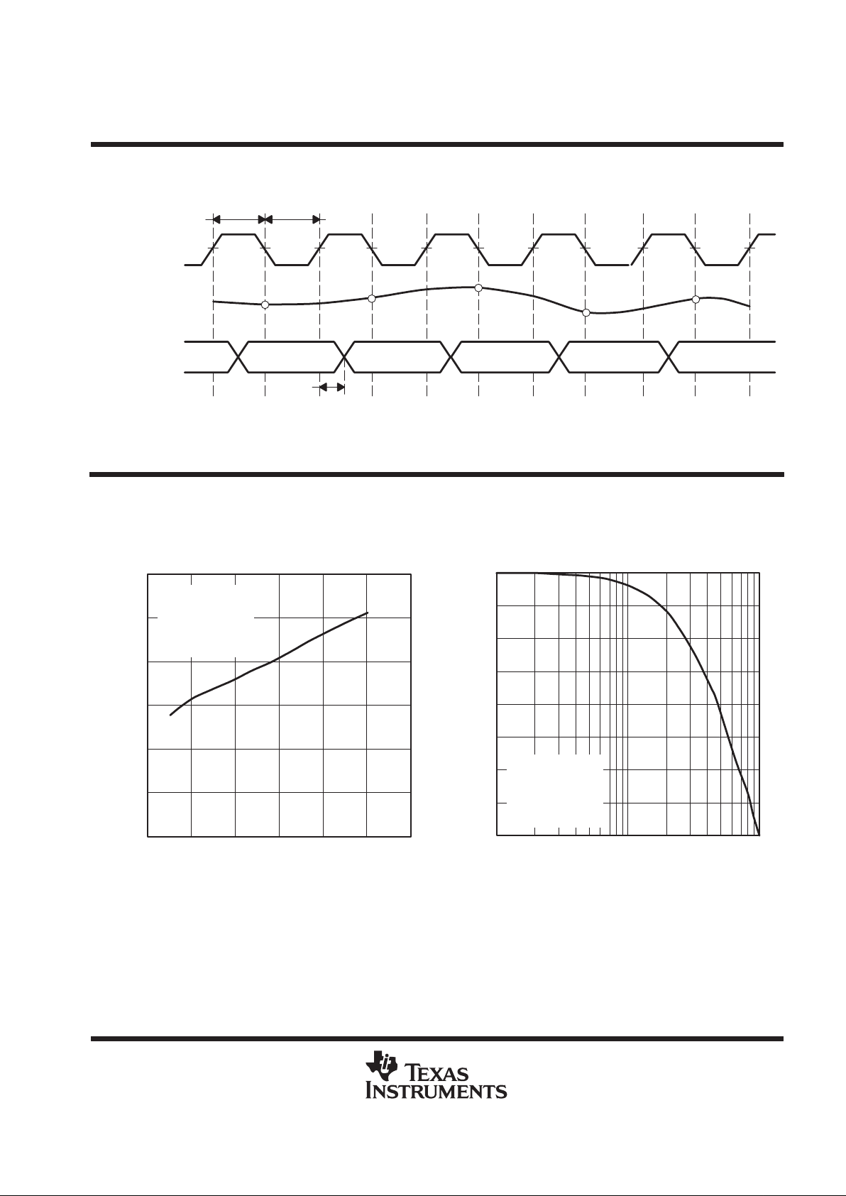
PARAMETER MEASUREMENT INFORMATION
N
N+1
N+2
N+3
N+4
N–3 N–2 N–1 N N+1
t
pd
CLK (Clock)
ANALOG IN
(Input Signal)
D1–D8
(Output Data)
t
w(H)
t
w(L)
Figure 1. I/O Timing Diagram
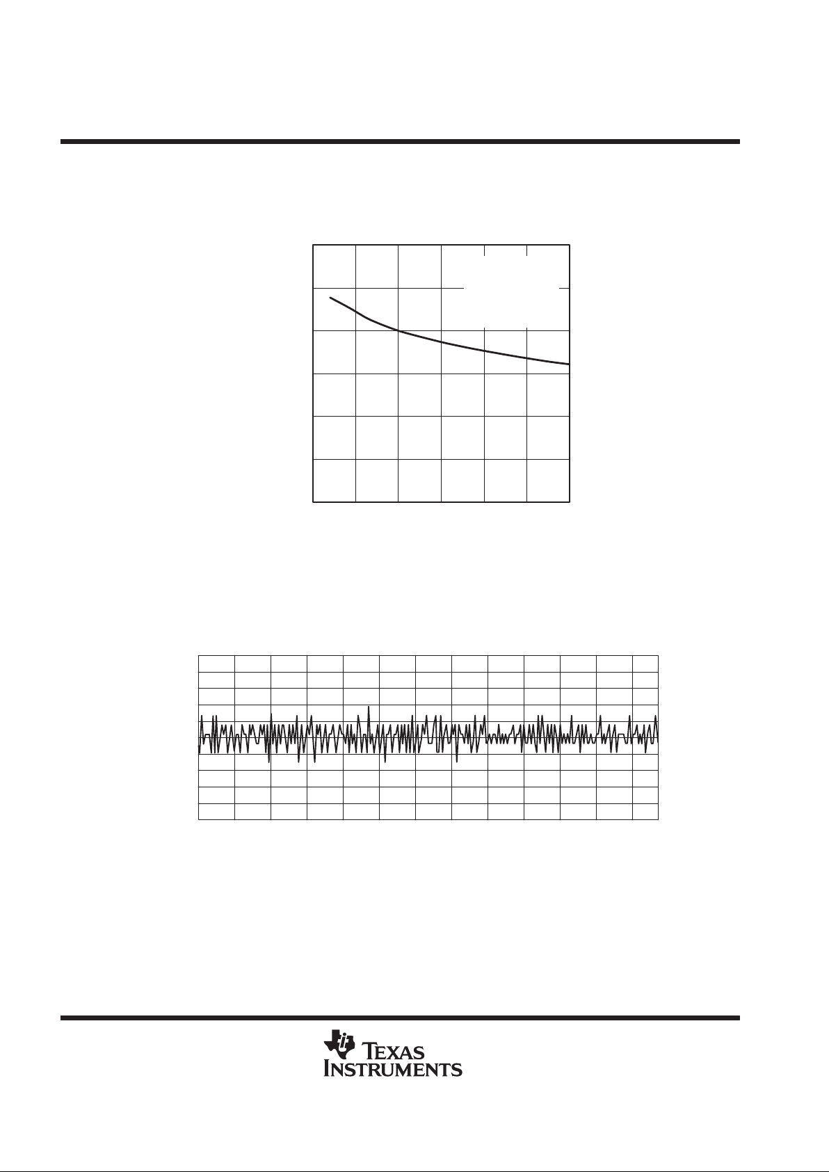
TYPICAL CHARACTERISTICS
Figure 2
6
4
2
0
02 4 6
Power Dissipation – mW
8
10
Sampling Frequency – MHz
POWER DISSIPATION
vs
SAMPLING FREQUENCY
12
81012
TA = 25°C
V
DDA
= 2.7 V,
V
REFB
= 0.5 V,
V
REFT
= 2.5 V,
Fclk = 10 MHz
Figure 3
10
0
–4
–5
–7
–8
–2
–1
0
Gain – dB
ANALOG INPUT BANDWIDTH
fI – Input Frequency – MHz
–3
–6
10
1
10
2
TA = 25°C
V
DDA
= 2.7 V,
V
REFB
= 0.5 V,
V
REFT
= 2.5 V,
Fclk = 10 MHz
TLV5510
2.7-V TO 3.6-V 8-BIT HIGH-SPEED ANALOG-TO-DIGITAL CONVERTER
SLAS124C– DECEMBER 1997 – REVISED DECEMBER 1999
6
POST OFFICE BOX 655303 • DALLAS, TEXAS 75265
TYPICAL CHARACTERISTICS
Figure 4
30
20
10
0
0 0.5 1 1.5
Signal-To-Noise Ratio – dB
40
50
Input Frequency – MHz
SIGNAL-TO-NOISE RATIO
vs
INPUT FREQUENCY
60
2 2.5 3
TA = 25°C
V
DDA
= 3 V,
V
REFB
= 0.5 V,
V
REFT
= 2.5 V,
Fclk = 10 MHz
0.2
–0.2
–0.3
–0.4
0 20 40 60 80 100 120
DNL – Differential Nonlinearity – LSB
0.3
0.4
Samples
0.5
140 160 180 200
0.1
0
–0.1
–0.5
220 240 253
DIFFERENTIAL NONLINEARITY
vs
SAMPLES
(Under Recommended Operating Conditions)
Figure 5

TLV5510
2.7-V TO 3.6-V 8-BIT HIGH-SPEED ANALOG-TO-DIGITAL CONVERTER
SLAS124C– DECEMBER 1997 – REVISED DECEMBER 1999
7
POST OFFICE BOX 655303 • DALLAS, TEXAS 75265
TYPICAL CHARACTERISTICS
6.35
6.3
6.25
–40 –20 0 20
Effective Number Of Bits
6.4
6.45
EFFECTIVE NUMBER OF BITS
vs
TEMPERATURE
6.5
40 60 80
Ambient Temperature – °C
V
DDA
= 3 V,
V
REFB
= 0.5 V,
V
REFT
= 2.5 V,
Fclk = 10 MHz,
f
sin
= 1 MHz
Figure 6
0.1
0
–0.1
–0.2
0 20 40 60 80 100 120
INL – Integral Nonlinearity – LSB
0.5
0.6
Samples
INTEGRAL NONLINEARITY
vs
SAMPLES
(Under Recommended Operating Conditions)
0.75
140 160 180 200
0.4
0.3
0.2
–0.3
–0.4
–0.5
–0.6
–0.75
220 240 254
Figure 7

TLV5510
2.7-V TO 3.6-V 8-BIT HIGH-SPEED ANALOG-TO-DIGITAL CONVERTER
SLAS124C– DECEMBER 1997 – REVISED DECEMBER 1999
8
POST OFFICE BOX 655303 • DALLAS, TEXAS 75265
TYPICAL CHARACTERISTICS
–60
–80
–100
–120
0 0.5 1 1.5 2 2.5 3
Fast Fourier Transformer – dB
–40
–20
f – Frequency – MHz
FAST FOURIER TRANSFORMER
vs
FREQUENCY
(Under Recommended Operating Conditions)
0
3.5 4 4.5 5
–140
–160
–180
–200
Figure 8
Figure 9
1
0.6
0.4
0
57 91113
INL – Integral Linearity – LSB
1.4
1.6
INTEGRAL LINEARITY ERROR
vs
FREQUENCY
1.8
15 17 19 21
1.2
0.8
0.2
f
CLK
– Frequency – MHz
V
DDD
= 2.7 V,
V
DDA
= 2.7 V,
V
REFT
= 2.5 V,
V
REFB
= 0.5 V
TA = 25°C
TA = –35°C
TA = 85°C
Figure 10
1
0.6
0.4
0
57 91113
1.4
1.6
15 17 19 21
1.2
0.8
0.2
f
CLK
– Frequency – MHz
DNL – Differential Linearity – LSB
DIFFERENTIAL LINEARITY ERROR
vs
FREQUENCY
1.8
TA = 25°C
TA = 85°C
TA = –35°C
V
DDD
= 2.7 V,
V
DDA
= 2.7 V,
V
REFT
= 2.5 V,
V
REFB
= 0.5 V

TLV5510
2.7-V TO 3.6-V 8-BIT HIGH-SPEED ANALOG-TO-DIGITAL CONVERTER
SLAS124C– DECEMBER 1997 – REVISED DECEMBER 1999
9
POST OFFICE BOX 655303 • DALLAS, TEXAS 75265
TYPICAL CHARACTERISTICS
Figure 11
1
0.6
0.4
0
57 91113
INL – Integral Linearity – LSB
1.4
1.6
INTEGRAL LINEARITY ERROR
vs
FREQUENCY
1.8
15 17 19 21
1.2
0.8
0.2
f
CLK
– Frequency – MHz
TA = 85°C
TA = 25°C
TA = –35°C
V
DDD
= 3 V,
V
DDA
= 3 V,
V
REFT
= 2.5 V,
V
REFB
= 0.5 V
Figure 12
1
0.6
0.4
0
57 91113
1.4
1.6
15 17 19 21
1.2
0.8
0.2
f
CLK
– Frequency – MHz
DNL – Differential Linearity – LSB
DIFFERENTIAL LINEARITY ERROR
vs
FREQUENCY
1.8
TA = 85°C
TA = 25°C
TA = –35°C
V
DDD
= 3 V,
V
DDA
= 3 V,
V
REFT
= 2.5 V,
V
REFB
= 0.5 V
Figure 13
1
0.6
0.4
0
57 91113
INL – Integral Linearity – LSB
1.4
1.6
INTEGRAL LINEARITY ERROR
vs
FREQUENCY
1.8
15 17 19 21
1.2
0.8
0.2
f
CLK
– Frequency – MHz
TA = 85°C
TA = 25°C
TA = –35°C
V
DDD
= 3.3 V,
V
DDA
= 3.3 V,
V
REFT
= 2.5 V,
V
REFB
= 0.5 V
Figure 14
1
0.6
0.4
0
57 91113
DNL – Differential Linearity – LSB
1.4
1.6
DIFFERENTIAL LINEARITY ERROR
vs
FREQUENCY
1.8
15 17 19 21
1.2
0.8
0.2
f
CLK
– Frequency – MHz
TA = 85°C
TA = 25°C
TA = –35°C
V
DDD
= 3.3 V,
V
DDA
= 3.3 V,
V
REFT
= 2.5 V,
V
REFB
= 0.5 V

TLV5510
2.7-V TO 3.6-V 8-BIT HIGH-SPEED ANALOG-TO-DIGITAL CONVERTER
SLAS124C– DECEMBER 1997 – REVISED DECEMBER 1999
10
POST OFFICE BOX 655303 • DALLAS, TEXAS 75265
TYPICAL CHARACTERISTICS
Figure 15
6.5
6
5.5
5
0 0.2 0.4 0.6 0.8
ENOB – Effective Number of Bits – Bits
7
7.5
f – Input Sinewave Frequency – MHz
EFFECTIVE NUMBER OF BITS
vs
INPUT SINEWAVE FREQUENCY
8
1 1.2 1.4
V
DDD
= 2.7 V,
V
DDA
= 2.7 V
TA = 85°C
TA = 25°C
TA = –35°C
Figure 16
6.5
6
5.5
5
0 0.2 0.4 0.6 0.8
ENOB – Effective Number of Bits – Bits
7
7.5
EFFECTIVE NUMBER OF BITS
vs
INPUT SINEWAVE FREQUENCY
8
1 1.2 1.4
f – Input Sinewave Frequency – MHz
TA = 85°C
TA = 25°C
TA = –35°C
V
DDD
= 3 V,
V
DDA
= 3 V
6.5
6
5.5
5
0 0.2 0.4 0.6 0.8
ENOB – Effective Number of Bits – Bits
7
7.5
EFFECTIVE NUMBER OF BITS
vs
INPUT SINEWAVE FREQUENCY
8
1 1.2 1.4
f – Input Sinewave Frequency – MHz
TA = 85°C
TA = 25°C
TA = –35°C
V
DDD
= 3.3 V,
V
DDA
= 3.3 V
Figure 17

TLV5510
2.7-V TO 3.6-V 8-BIT HIGH-SPEED ANALOG-TO-DIGITAL CONVERTER
SLAS124C– DECEMBER 1997 – REVISED DECEMBER 1999
11
POST OFFICE BOX 655303 • DALLAS, TEXAS 75265
APPLICATION INFORMATION
The following notes are design recommendations that should be used with the TLV5510.
D
External analog and digital circuitry should be physically separated and shielded as much as possible to
reduce system noise.
D
RF breadboarding or printed-circuit-board (PCB) techniques should be used throughout the evaluation and
production process. Breadboards should be copper clad for bench evaluation.
D
Since AGND and DGND are connected internally , the ground lead in must be kept as noise free as possible.
A good method to use is twisted-pair cables for the supply lines to minimize noise pickup. An analog and
digital ground plane should be used on PCB layouts when additional logic devices are used. The AGND
and DGND terminals of the device should be tied to the analog ground plane.
D
V
DDA
to AGND and V
DDD
to DGND should be decoupled with 1-µF and 0.01-µF capacitors, respectively ,
placed as close as possible to the appropriate device terminals. A ceramic chip capacitor is recommended
for the 0.01-µF capacitor. Care should be exercised to assure a solid noise-free ground connection for the
analog and digital grounds.
D
V
DDA
, AGND, and ANALOG IN terminals should be shielded from the higher frequency terminals, CLK and
D0–D7. If possible, AGND traces should be placed on both sides of the ANALOG IN traces on the PCB for
shielding.
D
In testing or application of the device, the resistance of the driving source connected to the analog input
should be 10 Ω or less within the analog frequency range of interest.

TLV5510
2.7-V TO 3.6-V 8-BIT HIGH-SPEED ANALOG-TO-DIGITAL CONVERTER
SLAS124C– DECEMBER 1997 – REVISED DECEMBER 1999
12
POST OFFICE BOX 655303 • DALLAS, TEXAS 75265
APPLICATION INFORMATION
14
15
18
16
17
19
22
23
20
21
13
11
10
9
8
7
6
5
4
3
12
1
2
24
C8
C9
V
DDA
V
DDA
V
DDA
REFTS
REFT
ANALOG IN
REFBS
REFB
AGND
AGND
DV
DDD
DV
DDD
D8
D7
D6
D5
D4
D3
D2
D1
CLK
OE
DGND
DGND
FB3
FB2
FB1
C3
C4
C5
C6
C7
C2
Buffer
C1
From Clamp
Output
Video Input
(2VPP)
A
V
DDA
3.3 V
V
DDD
3.3 V
Output Enable
Clock
D
C10
R1
+
LOCATION
DESCRIPTION
C1, C3, C4 –C9 0.1 µF Capacitor
C2 10 pF Capacitor
C10 47 µF Capacitor
FB1, FB2, FB3 Ferrite bead
R1 75 Ω Resistor
Figure 18. Application and Test Schematic Using Internal Reference

TLV5510
2.7-V TO 3.6-V 8-BIT HIGH-SPEED ANALOG-TO-DIGITAL CONVERTER
SLAS124C– DECEMBER 1997 – REVISED DECEMBER 1999
13
POST OFFICE BOX 655303 • DALLAS, TEXAS 75265
PRINCIPLES OF OPERATION
functional description
The TLV5510 is a semiflash ADC featuring two lower comparator blocks of four bits each.
As shown in Figure 19, input voltage V
I
(1) is sampled with the falling edge of CLK1 to the upper comparators
block and the lower comparators block(A), S(1). The upper comparators block finalizes the upper data UD(1)
with the rising edge of CLK2, and simultaneously, the lower reference voltage generates the voltage RV(1)
corresponding to the upper data. The lower comparators block (A) finalizes the lower data LD(1) with the rising
edge of CLK3. UD(1) and LD(1) are combined and output as OUT(1) with the rising edge of CLK4. According
to the above internal operation described, output data is delayed 2.5 clocks from the analog input voltage
sampling point.
Input voltage V
I
(2) is sampled with the falling edge of CLK2. UD(2) is finalized with the rising edge of CLK3, and
LD(2) is finalized with the rising edge of CLK4 at the lower comparators block(B). OUT(2) is output with the rising
edge of CLK5.
VI(1) VI(2) VI(3) VI(4)
CLK1 CLK2 CLK3 CLK4
S(1) C(1) S(2) C(2) S(3) C(3) S(4) C(4)
S(1) H(1) C(1) S(3) H(3) C(3)
H(0) C(0) S(2) H(2) C(2) S(4) H(4)
LD(–2)
OUT(–2) OUT(–1) OUT(0) OUT(1)
ANALOG IN
(Sampling Points)
CLK (Clock)
Upper Comparators Block
Upper Data
Lower Reference Voltage
Lower Comparators Block (A)
Lower Data (A)
Lower Comparators Block (B)
Lower Data (B)
D1–D8 (Data Output)
UD(0)
RV(0)
UD(1)
RV(1)
UD(2)
RV(2)
UD(3)
RV(3)
LD(–1)
LD(0)
LD(1)
LD(2)
Figure 19. Internal Functional Timing Diagram

TLV5510
2.7-V TO 3.6-V 8-BIT HIGH-SPEED ANALOG-TO-DIGITAL CONVERTER
SLAS124C– DECEMBER 1997 – REVISED DECEMBER 1999
14
POST OFFICE BOX 655303 • DALLAS, TEXAS 75265
PRINCIPLES OF OPERATION
functional description (continued)
The MSB comparator block converts on the falling edge of each applied clock cycle. The LSB comparator blocks
CB-A and CB-B convert on the falling edges of the first and second following clock cycles, respectively. The
timing diagram of the conversion algorithm is shown in Figure 19.
analog input operation
The analog input stage to the TLV5510 is a chopper-stabilized comparator and is equivalently shown below:
V
DDA
ANALOG IN
S1
V
ref(N)
φ1
φ2
φ2
S3
φ1
C
s
To Encoder Logic
φ2
S2
φ1
C
s
To Encoder Logic
φ2
S(N)
φ1
C
s
To Encoder Logic
Figure 20. External Connections for Using the Internal Reference Resistor Divider
Figure 20 depicts the analog input for the TL V5510. The switches shown are controlled by two internal clocks,
φ1 and φ2. These are nonoverlapping clocks that are generated from the CLK input. During the sampling period,
φ1, S1 is closed and the input signal is applied to one side of the sampling capacitor, C
s
. Also during the sampling
period, S2 through S(N) are closed. This sets the comparator input to approximately 2.5 V. The delta voltage
is developed across Cs. During the comparison phase, φ2, S1 is switched to the appropriate reference voltage
for the bit value N, i.e., V
ref(N)
. S2 is opened and V
ref(N)
– VC
s
toggles the comparator output to the appropriate
digital 1 or 0. The small resistance values for the switch, S1, and small value of the sampling capacitor combine
to produce the wide analog input bandwidth of the TLV5510. The source impedance driving the analog input
of the TLV5510 should be less than 100 Ω across the range of input frequency spectrum.
reference inputs – REFB, REFT, REFBS, REFTS
The range of analog inputs that can be converted are determined by REFB and REFT, REFT being the
maximum reference voltage and REFB being the minimum reference voltage. The TLV5510 is tested with
REFT = 2.5 V or 2 V and REFB = 0.5 V or 0 V producing a 2-V full-scale range. The TL V5510 can operate with
REFT – REFB = 2.4 V , but the power dissipation in the reference resistor increases significantly (49 mW at 3.3 V
nominally). It is recommended that a 0.1 µF capacitor be attached to REFB and REFT whether using externally
or internally generated voltages.
TLV5510
2.7-V TO 3.6-V 8-BIT HIGH-SPEED ANALOG-TO-DIGITAL CONVERTER
SLAS124C– DECEMBER 1997 – REVISED DECEMBER 1999
15
POST OFFICE BOX 655303 • DALLAS, TEXAS 75265
PRINCIPLES OF OPERATION
internal reference voltage conversion
Three internal resistors allow the device to generate an internal reference voltage. These resistors are brought
out on terminals V
DDA
, REFTS, REFT, REFB, REFBS, and AGND. Two different bias voltages are possible
without the use of external resistors.
The internal resistors are provided to develop REFT and REFB as listed in T able 1 (bias option 1) with only two
external connections. This is developed with a 3-resistor network connected to V
DDA
. When using this feature,
connect REFT to REFTS and connect REFB to REFBS. For applications where the variance associated with
V
DDA
is acceptable, this internal voltage reference saves space and cost (see Figure 21).
A second internal bias option (bias two option) is shown in Figure 22. Using this scheme REFB = AGND and
REFT is as shown in T able 1 (bias option 2). These bias voltage options can be used to provide the values listed
in the following table.
Table 1. Bias Voltage Options for Different V
DDA
BIAS VOLTAGE
BIAS OPTION
V
DDA
V
REFB
V
REFT
V
REFT
– V
REFB
2.7 V 0.54 2.34 1.8
3 V 0.6 2.60 2
1
3.3 V 0.66 2.86 2.2
3.6 V 0.72 3.12 2.4
2.7 V AGND 2.25 2.25
3 V AGND 2.5 2.5
2
3.3 V AGND 2.75 2.75
3.6 V AGND 3 3
To use the internally-generated reference voltage, terminal connections should be made as shown in
Figure 21 or Figure 22.
R1
40 Ω NOM
R
ref
200 Ω NOM
R2
60 Ω NOM
V
DDA
REFTS
REFT
REFB
REFBS
AGND
TLV5510
16
17
22
21
23
18
0.1 µF
0.1 µF
2.63 V dc
Figure 21. External Connections Using the Internal Bias One Option

TLV5510
2.7-V TO 3.6-V 8-BIT HIGH-SPEED ANALOG-TO-DIGITAL CONVERTER
SLAS124C– DECEMBER 1997 – REVISED DECEMBER 1999
16
POST OFFICE BOX 655303 • DALLAS, TEXAS 75265
PRINCIPLES OF OPERATION
R1
40 Ω NOM
R
ref
200 Ω NOM
R2
60 Ω NOM
V
DDA
(Analog Supply)
REFTS
REFT
REFB
REFBS
AGND
TLV5510
16
17
22
21
23
18
0.1 µF
Figure 22. External Connections for Using the Internal Reference Resistor Divider
functional operation
The TLV5510 functions as shown in the Table 2.
Table 2. Functional Operation
INPUT SIGNAL
DIGITAL OUTPUT CODE
INPUT SIGNAL
VOLTAGE
STEP
MSB LSB
REFT 255 1 1 1 1 1 1 1 1
•
• • •••••••
• • • •••••••
• 128 1 0000000
• 127 0 1111111
• • • •••••••
• • • •••••••
REFB 0 0 0 0 0 0 0 0 0

TLV5510
2.7-V TO 3.6-V 8-BIT HIGH-SPEED ANALOG-TO-DIGITAL CONVERTER
SLAS124C– DECEMBER 1997 – REVISED DECEMBER 1999
17
POST OFFICE BOX 655303 • DALLAS, TEXAS 75265
MECHANICAL DATA
PW (R-PDSO-G**) PLASTIC SMALL-OUTLINE PACKAGE
14 PINS SHOWN
0,65
M
0,10
0,10
0,25
0,50
0,75
0,15 NOM
Gage Plane
28
9,80
9,60
24
7,90
7,70
2016
6,60
6,40
4040064/F 01/97
0,30
6,60
6,20
8
0,19
4,30
4,50
7
0,15
14
A
1
1,20 MAX
14
5,10
4,90
8
3,10
2,90
A MAX
A MIN
DIM
PINS **
0,05
4,90
5,10
Seating Plane
0°–8°
NOTES: A. All linear dimensions are in millimeters.
B. This drawing is subject to change without notice.
C. Body dimensions do not include mold flash or protrusion not to exceed 0,15.
D. Falls within JEDEC MO-153

TLV5510
2.7-V TO 3.6-V 8-BIT HIGH-SPEED ANALOG-TO-DIGITAL CONVERTER
SLAS124C– DECEMBER 1997 – REVISED DECEMBER 1999
18
POST OFFICE BOX 655303 • DALLAS, TEXAS 75265
MECHANICAL DATA
NS (R-PDSO-G**) PLASTIC SMALL-OUTLINE PACKAGE
4040062/B 2/95
14 PIN SHOWN
2,00 MAX
A
0,05 MIN
Seating Plane
1,05
0,55
1
14
PINS **
5,60
5,00
7
8,20
7,40
8
A MIN
A MAX
DIM
Gage Plane
0,15 NOM
0,25
9,90 9,90
10,501410,50
16
12,30 14,70
15,3012,90
20 24
0,10
1,27
0°–10°
M
0,25
0,35
0,51
NOTES: A. All linear dimensions are in millimeters.
B. This drawing is subject to change without notice.
C. Body dimensions do not include mold flash or protrusion, not to exceed 0,15.

IMPORTANT NOTICE
T exas Instruments and its subsidiaries (TI) reserve the right to make changes to their products or to discontinue
any product or service without notice, and advise customers to obtain the latest version of relevant information
to verify, before placing orders, that information being relied on is current and complete. All products are sold
subject to the terms and conditions of sale supplied at the time of order acknowledgement, including those
pertaining to warranty, patent infringement, and limitation of liability.
TI warrants performance of its semiconductor products to the specifications applicable at the time of sale in
accordance with TI’s standard warranty. Testing and other quality control techniques are utilized to the extent
TI deems necessary to support this warranty. Specific testing of all parameters of each device is not necessarily
performed, except those mandated by government requirements.
CERT AIN APPLICATIONS USING SEMICONDUCTOR PRODUCTS MAY INVOLVE POTENTIAL RISKS OF
DEATH, PERSONAL INJURY, OR SEVERE PROPERTY OR ENVIRONMENTAL DAMAGE (“CRITICAL
APPLICATIONS”). TI SEMICONDUCTOR PRODUCTS ARE NOT DESIGNED, AUTHORIZED, OR
WARRANTED TO BE SUITABLE FOR USE IN LIFE-SUPPORT DEVICES OR SYSTEMS OR OTHER
CRITICAL APPLICATIONS. INCLUSION OF TI PRODUCTS IN SUCH APPLICA TIONS IS UNDERSTOOD T O
BE FULLY AT THE CUSTOMER’S RISK.
In order to minimize risks associated with the customer’s applications, adequate design and operating
safeguards must be provided by the customer to minimize inherent or procedural hazards.
TI assumes no liability for applications assistance or customer product design. TI does not warrant or represent
that any license, either express or implied, is granted under any patent right, copyright, mask work right, or other
intellectual property right of TI covering or relating to any combination, machine, or process in which such
semiconductor products or services might be or are used. TI’s publication of information regarding any third
party’s products or services does not constitute TI’s approval, warranty or endorsement thereof.
Copyright 1999, Texas Instruments Incorporated
 Loading...