

Datasheet TLV4112IP, TLV4112IDR, TLV4112ID, TLV4112CP, TLV4112CDR Datasheet (Texas Instruments)
...
TLV4110, TLV4111, TLV4112, TLV4113
FAMILY OF HIGH OUTPUT DRIVE OPERATIONAL
AMPLIFIERS WITH SHUTDOWN
SLOS289A – DECEMBER 1999 – REVISED APRIL 2000
1
POST OFFICE BOX 655303 • DALLAS, TEXAS 75265
D
High Output Drive . . . >300 mA
D
Rail-To-Rail Output
D
Unity-Gain Bandwidth ...2 MHz
D
Slew Rate . . . 1.5 V/µs
D
Supply Current . . . 700-µA/Per Channel
D
Supply Voltage Range . . . 2.5 V to 6 V
D
Specified Temperature Range:
– TA = 0°C to 70°C . . . Commercial Grade
– TA = –40°C to 125°C . . . Industrial Grade
D
Universal OpAmp EVM
description
The TLV411x single supply operational amplifiers provide output currents in excess of 300 mA at 5 V. This
enables standard pin-out amplifiers to be used as high current buffers or in coil driver applications. The TL V4110
and TLV41 13 comes with a shutdown feature.
The TLV411x is available in the ultra small MSOP PowerPAD package, which of fers the exceptional thermal
impedance required for amplifiers delivering high current levels.
All TLV41 1x devices are offered in PDIP, SOIC (single and dual) and MSOP PowerPAD (dual).
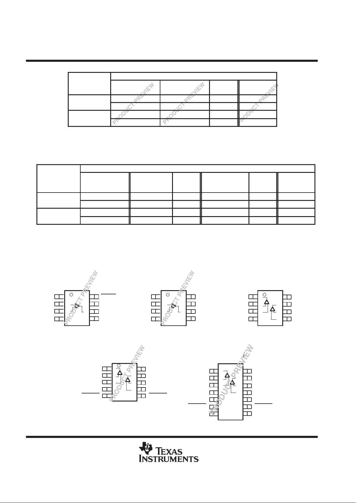
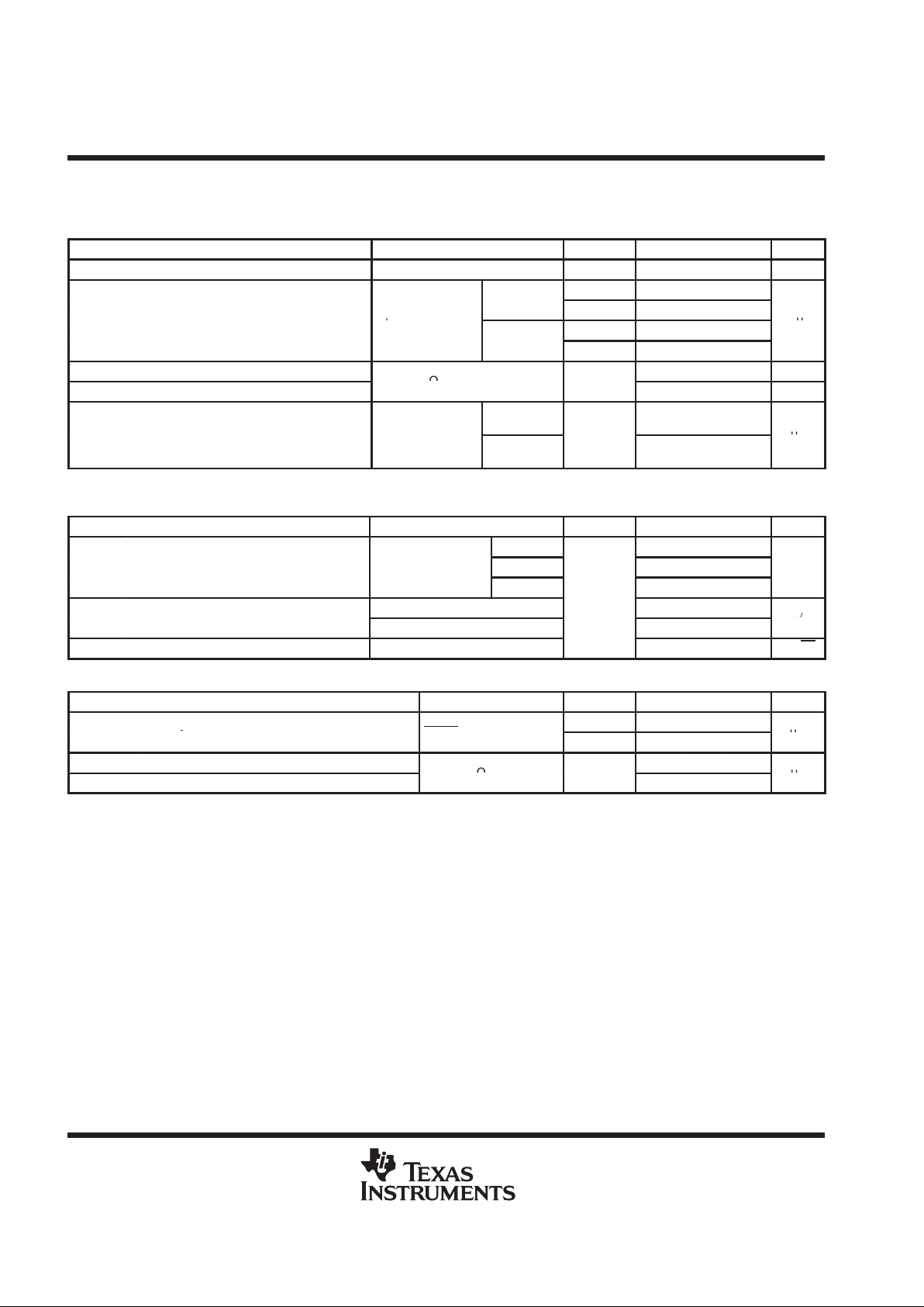
FAMILY PACKAGE TABLE
NUMBER OF
PACKAGE TYPES
UNIVERSAL
DEVICE
CHANNELS
MSOP PDIP SOIC
SHUTDOWN
EVM BOARD
TLV4110
†
1 8 8 8 Yes
TLV4111
†
1 8 8 8 —
Refer to the EVM
TLV4112 2 8 8 8 —
Selecti
on Guide
(
Lit# SL
OU060)
TLV4113
†
2 10 14 14 Yes
(Lit# SLOU060)
†
This device is in the Product Preview stage of development. Contact the local TI sales office for more
information.
HIGH-LEVEL OUTPUT VOLTAGE
vs
HIGH-LEVEL OUTPUT CURRENT
VDD = 3 V
IOH – High-Level Output Current – mA
V
OH
– High-Level Output Voltage – V
TA = 70°C
TA = 25°C
TA = 0°C
TA = –40°C
3.0
2.9
2.8
2.7
2.6
2.5
2.4
2.3
2.0
0 50 200100 150 250 300
2.2
2.1
TA = 125°C
TA = –40°C
LOW-LEVEL OUTPUT VOLTAGE
vs
LOW-LEVEL OUTPUT CURRENT
VDD = 3 V
IOL – Low-Level Output Current – mA
TA = 70°C
TA = 25°C
TA = 0°C
OL
V – Low-Level Output Voltage – V
1.0
0.9
0.8
0.7
0.6
0.5
0.4
0.3
0.0
0 50 200100 150 250 300
0.2
0.1
TA = 125°C
Copyright 2000, Texas Instruments Incorporated
PRODUCTION DATA information is current as of publication date.
Products conform to specifications per the terms of Texas Instruments
standard warranty. Production processing does not necessarily include
testing of all parameters.
Please be aware that an important notice concerning availability, standard warranty, and use in critical applications of
Texas Instruments semiconductor products and disclaimers thereto appears at the end of this data sheet.
1
2
3
4
8
7
6
5
1OUT
1IN–
1IN+
GND
V
DD
2OUT
2IN–
2IN+
TLV4112
D, DGN, OR P PACKAGE
(TOP VIEW)
PowerPAD is a trademark of Texas Instruments.
TLV4110, TLV4111, TLV4112, TLV4113
FAMILY OF HIGH OUTPUT DRIVE OPERATIONAL
AMPLIFIERS WITH SHUTDOWN
SLOS289A – DECEMBER 1999 – REVISED APRIL 2000
2
POST OFFICE BOX 655303 • DALLAS, TEXAS 75265
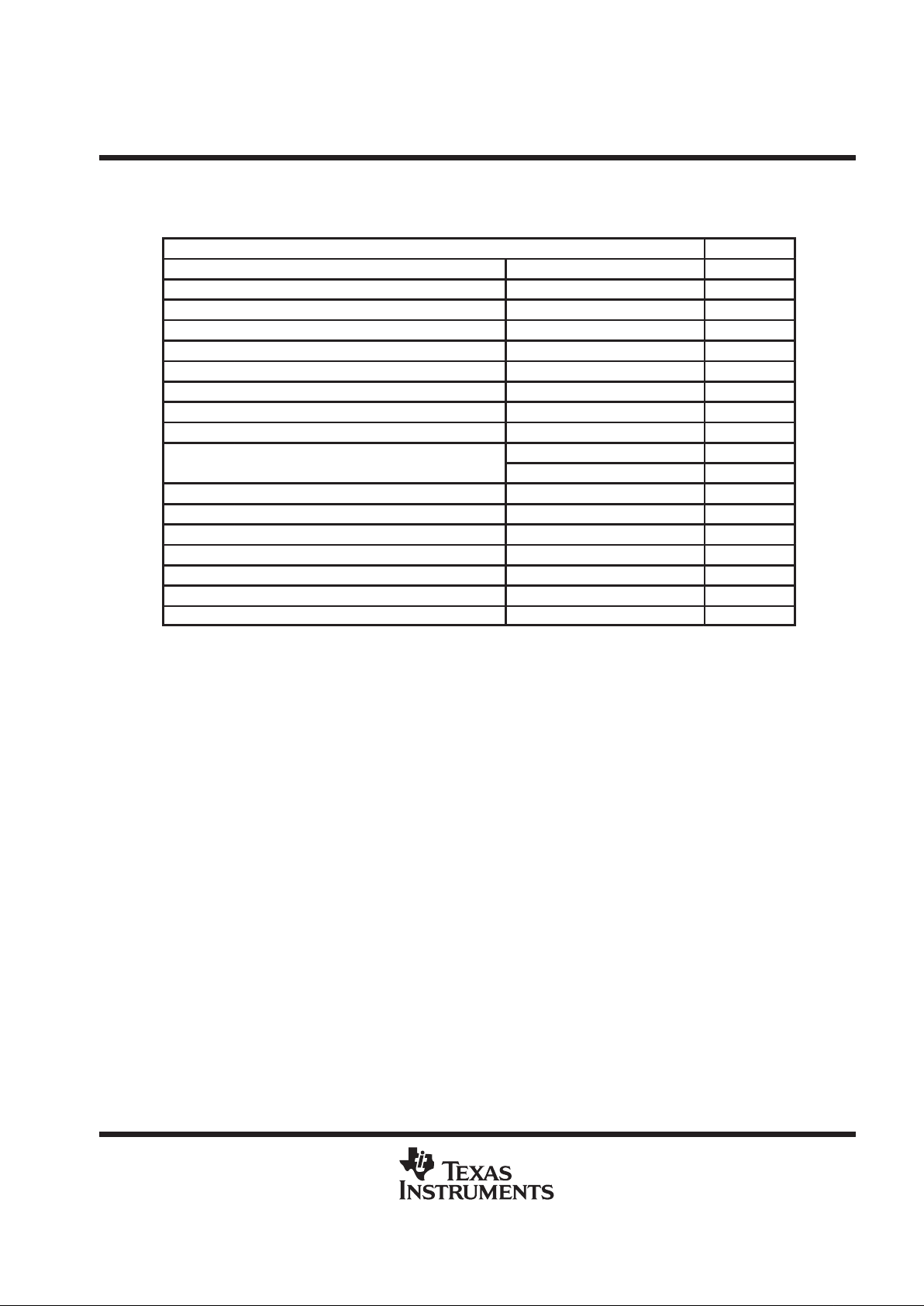
TLV4110 AND TLV4111 AVAILABLE OPTIONS
PACKAGED DEVICES
T
A
SMALL OUTLINE SMALL OUTLINE
PLASTIC DIP
(D)
†‡
(DGN)
†
SYMBOL
(P)
°
°
TLV4110CD TLV4110CDGN xxTIAHL TLV4110CP
0°C to 70°C
TLV4111CD TLV4111CDGN xxTIAHN TLV4111CP
°
°
TLV4110ID TLV4110IDGN xxTIAHM TLV4110IP
–
40°C to 125°C
TLV4111ID TLV4111IDGN xxTIAHO TLV4111IP
†
This package is available taped and reeled. T o order this packaging option, add an R suf fix to the part
number (e.g., TL V4110CDR).
‡
In the SOIC package, the maximum RMS output power is thermally limited to 350 mW; 700 mW peaks can be driven, as
long as the RMS value is less than 350 mW.
TLV4112 AND TLV4113 AVAILABLE OPTIONS
PACKAGED DEVICES
T
A
SMALL OUTLINE
SMALL OUT-
SMALL OUTLINE
PLASTIC DIP
(D)
†§
LINE
(DGN)
†
SYMBOL
(DGQ)
†
SYMBOL
(P)
°
°
TLV4112CD TLV4112DGN xxTIAHP — — TLV4112CP
0°C to 70°C
TLV4113CD
‡
— — TLV4113CDGN
‡
xxTIAHR TLV4113CN
‡
°
°
TLV4112ID TLV4112IDGN xxTIAHQ — — TLV4112IP
–
40°C to 125°C
TLV4113ID
‡
— — TLV4113IDGN
‡
xxTIAHS TLV4113IN
‡
†
This package is available taped and reeled. To order this packaging option, add an R suffix to the part number (e.g., TLV4112CDR).
‡
This device is in the Product Preview stage of development. Contact the local TI sales office for more information.
§
In the SOIC package, the maximum RMS output power is thermally limited to 350 mW; 700 mW peaks can be driven, as long as the
RMS value is less than 350 mW.
TLV411x PACKAGE PINOUTS
1
2
3
4
5
6
7
14
13
12
11
10
9
8
1OUT
1IN–
1IN+
GND
NC
1SHDN
NC
V
DD
2OUT
2IN–
2IN+
NC
2SHDN
NC
(TOP VIEW)
1
2
3
4
8
7
6
5
NC
IN–
IN+
GND
SHDN
NC
V
DD
OUT
TLV4110
D, DGN OR P PACKAGE
(TOP VIEW)
1
2
3
4
8
7
6
5
1OUT
1IN–
1IN+
GND
V
DD
2OUT
2IN–
2IN+
TLV4112
D, DGN, OR P PACKAGE
(TOP VIEW)
TLV4113
D OR N PACKAGE
NC – No internal connection
1
2
3
4
5
10
9
8
7
6
1OUT
1IN–
1IN+
GND
1SHDN
VDD+
2OUT
2IN–
2IN+
2SHDN
TLV4113
DGQ PACKAGE
(TOP VIEW)
1
2
3
4
8
7
6
5
NC
IN–
IN+
GND
NC
V
DD
OUT
NC
TLV4111
D, DGN OR P PACKAGE
(TOP VIEW)
TLV4110, TLV4111, TLV4112, TLV4113
FAMILY OF HIGH OUTPUT DRIVE OPERATIONAL
AMPLIFIERS WITH SHUTDOWN
SLOS289A – DECEMBER 1999 – REVISED APRIL 2000
3
POST OFFICE BOX 655303 • DALLAS, TEXAS 75265
absolute maximum ratings over operating free-air temperature range (unless otherwise noted)
†
Supply voltage, VDD (see Note 1) 7 V. . . . . . . . . . . . . . . . . . . . . . . . . . . . . . . . . . . . . . . . . . . . . . . . . . . . . . . . . . . . .
Differential input voltage, VID ±V
DD
. . . . . . . . . . . . . . . . . . . . . . . . . . . . . . . . . . . . . . . . . . . . . . . . . . . . . . . . . . . . . .
Input voltage range, V
I
±V
DD
. . . . . . . . . . . . . . . . . . . . . . . . . . . . . . . . . . . . . . . . . . . . . . . . . . . . . . . . . . . . . . . . . . . .
Output current,IO (see Note 2) 800 mA. . . . . . . . . . . . . . . . . . . . . . . . . . . . . . . . . . . . . . . . . . . . . . . . . . . . . . . . . . . .
Continuous /RMS output current, IO (each output of amplifier): TJ ≤ 105°C 350 mA. . . . . . . . . . . . . . . . . . . .
TJ ≤ 150°C 110 mA. . . . . . . . . . . . . . . . . . . .
Peak output current, IO (each output of amplifier: TJ ≤ 105°C 500 mA. . . . . . . . . . . . . . . . . . . . . . . . . . . . . . . .
T
J
≤ 150°C 155 mA. . . . . . . . . . . . . . . . . . . . . . . . . . . . . . . .
Continuous total power dissipation See Dissipation Rating Table. . . . . . . . . . . . . . . . . . . . . . . . . . . . . . . . . . . . .
Operating free-air temperature range, TA: C suffix 0°C to 70°C. . . . . . . . . . . . . . . . . . . . . . . . . . . . . . . . . . . . . .
I suffix –40°C to 125°C. . . . . . . . . . . . . . . . . . . . . . . . . . . . . . . . . . . .
Maximum junction temperature, T
J
150°C. . . . . . . . . . . . . . . . . . . . . . . . . . . . . . . . . . . . . . . . . . . . . . . . . . . . . . . . .
Storage temperature range, T
stg
–65°C to 150°C. . . . . . . . . . . . . . . . . . . . . . . . . . . . . . . . . . . . . . . . . . . . . . . . . . .
Lead temperature 1,6 mm (1/16 inch) from case for 10 seconds 260°C. . . . . . . . . . . . . . . . . . . . . . . . . . . . . . .
†
Stresses beyond those listed under “absolute maximum ratings” may cause permanent damage to the device. These are stress ratings only, and
functional operation of the device at these or any other conditions beyond those indicated under “recommended operating conditions” is not
implied. Exposure to absolute-maximum-rated conditions for extended periods may affect device reliability.
NOTES: 1. All voltage values, except differential voltages, are with respect to GND.
2. To prevent permanent damage the die temperature must not exceed the maximum junction temperature.
DISSIPATION RATING TABLE
PACKAGE
θ
JC
(°C/W)
θ
JA
(°C/W)
TA ≤ 25°C
POWER RATING
D (8) 38.3 176 710 mW
D (14) 26.9 122.3 1022 mW
DGN (8)
‡
4.7 52.7 2.37 W
DGQ (10)
‡
4.7 52.3 2.39 W
P (8) 41 104 1200 mW
N (14) 32 78 1600 mW
‡
See The Texas Instruments document,
PowerPAD Thermally Enhanced Package Application
Report
(literature number SLMA002), for more information on the PowerPAD package. The
thermal data was measured on a PCB layout based on the information in the section entitled
Texas Instruments Recommended Board for PowerPAD
on page 33 of the before mentioned
document.
recommended operating conditions
MIN MAX UNIT
Supply voltage, V
DD
2.5 6 V
Common-mode input voltage range, V
ICR
0 VDD–1.5 V
p
p
C-suffix 0 70
°
Operating free-air temperature, T
A
I-suffix –40 125
°C
VDD = 3 V 2.1
V(on)
VDD = 5 V 3.8
Shutdown turn on/off voltage level
§
VDD = 3 V 0.9
V
V(off)
VDD = 5 V 1.65
§
Relative to GND
TLV4110, TLV4111, TLV4112, TLV4113
FAMILY OF HIGH OUTPUT DRIVE OPERATIONAL
AMPLIFIERS WITH SHUTDOWN
SLOS289A – DECEMBER 1999 – REVISED APRIL 2000
4
POST OFFICE BOX 655303 • DALLAS, TEXAS 75265
electrical characteristics at recommend operating conditions, VDD = 3 V and 5 V (unless otherwise
noted)
dc performance
PARAMETER TEST CONDITIONS T
A
†
MIN TYP MAX UNITS
p
25°C 175 3500
VIOInput offset voltage
VIC = VDD/2,
VO = VDD/2 ,
Full range 4000
µ
V
αVIO Offset voltage draft
R
L
=
100 Ω
,
R
S
= 50
Ω
25°C 3 µV/°C
VDD = 3 V,
RS = 50 Ω
VIC = 0 to 2 V,
25°C 63
CMRR
Common-mode rejection ratio
VDD = 5 V,
RS = 50 Ω
VIC = 0 to 4 V,
25°C 68
dB
25°C 78 84
V
= 3 V,
R
L
=
100 Ω
Full range 67
DD
,
V
O(PP)
=0 to 1V
25°C 85 100
Large-signal differential voltage
R
L
=10
kΩ
Full range 75
A
VD
gg g
amplification
25°C 88 94
dB
V
= 5 V,
R
L
=
100 Ω
Full range 75
DD
,
V
O(PP)
=0 to 3V
25°C 90 110
R
L
=
10 kΩ
Full range 85
†
Full range is 0°C to 70°C for C suffix and –40°C to 125°C for I suffix. If not specified, full range is –40°C to 125°C.
input characteristics
PARAMETER TEST CONDITIONS T
A
†
MIN TYP MAX UNITS
p
Measured over
VDD = 3 V
25°C and
Full range
0
to
1.5
V
ICR
Common-mode input voltage range
CMRR
range,
RS = 50 Ω
VDD = 5 V
25°C and
Full range
0
to
3.5
V
25°C 0.3 25
I
IO
Input offset current VIC = VDD/2
TLV411xC
50
TLV411xI
Full range
250
p
25°C 0.3 50
pA
I
IB
Input bias current
VO = VDD/2,
TLV411xC
100
R
S
= 50
Ω
TLV411xI
Full range
500
r
i(d)
Differential input resistance 25°C 1000 GΩ
C
IC
Common-mode input capacitance f = 100 Hz 25°C 5 pF
†
Full range is 0°C to 70°C for C suffix and –40°C to 125°C for I suffix. If not specified, full range is –40°C to 125°C.
TLV4110, TLV4111, TLV4112, TLV4113
FAMILY OF HIGH OUTPUT DRIVE OPERATIONAL
AMPLIFIERS WITH SHUTDOWN
SLOS289A – DECEMBER 1999 – REVISED APRIL 2000
5
POST OFFICE BOX 655303 • DALLAS, TEXAS 75265
electrical characteristics at specified free-air temperature, VDD = 3 V and 5 V (unless otherwise
noted) (continued)
output characteristics
PARAMETER TEST CONDITIONS T
A
†
MIN TYP MAX UNITS
25°C 2.7 2.97
I
OH
= –10
mA
Full range 2.7
V
DD
=
3 V
,
V
IC
=
VDD/2
25°C 2.6 2.73
V
I
OH
=–
100 mA
Full range 2.6
25°C 4.7 4.96
V
OH
High-level output voltage
I
OH
= –10
mA
Full range 4.7
25°C 4.6 4.76
VDD = 5 V, VIC = VDD/2
I
OH
= –
100 mA
Full range 4.6
V
25°C 4.45 4.6
IOH = –200 mA
–40°C to
85°C
4.35
25°C 0.03 0.1
V
= 3 V and 5 V,
I
OL
= 10
mA
Full range 0.1
DD
,
VIC = VDD/2
25°C 0.33 0.4
V
OL
Low–level output voltage
I
OL
=
100 mA
Full range 0.55
V
25°C 0.38 0.6
VDD = 5 V, VIC = VDD/2 IOL = 200 mA
–40°C to
85°C
0.7
p
VDD = 3 V
°
±220
IOOutput current
‡
Measured at 0.5 V from rail
VDD = 5 V
25°C
±320
mA
p
Sourcing
°
800
IOSShort-circuit output current
‡
Sinking
25°C
800
mA
†
Full range is 0°C to 70°C for C suffix and –40°C to 125°C for I suffix. If not specified, full range is –40°C to 125°C.
‡
When driving output currents in excess of 200 mA, the MSOP PowerPAD package is required for thermal dissipation.
power supply
PARAMETER TEST CONDITIONS T
A
MIN TYP MAX UNITS
pp
p
25°C 700 1000
IDDSupply current (per channel)
V
O
=
VDD/2
Full range 1500
µ
A
V
=2.7 to 3.3 V , No load,
25°C 70 82
pp
DD
,
VIC = VDD/2 V
,
Full range 65
K
SVR
Power supply rejection ratio (∆V
DD
/
∆VIO)
VDD =4.5 to 5.5 V , No load,
25°C 70 79
dB
DD
VIC = VDD/2 V
Full range 65
†
Full range is 0°C to 70°C for C suffix and –40°C to 125°C for I suffix. If not specified, full range is –40°C to 125°C.
TLV4110, TLV4111, TLV4112, TLV4113
FAMILY OF HIGH OUTPUT DRIVE OPERATIONAL
AMPLIFIERS WITH SHUTDOWN
SLOS289A – DECEMBER 1999 – REVISED APRIL 2000
6
POST OFFICE BOX 655303 • DALLAS, TEXAS 75265
electrical characteristics at specified free-air temperature, VDD = 3 V and 5 V (unless otherwise
noted) (continued)
dynamic performance
PARAMETER TEST CONDITIONS T
A
†
MIN TYP MAX UNITS
GBWP Gain bandwidth product RL=100 Ω CL=10 pF 25°C 2.7 MHz
25°C 0.8 1.57
V
o(pp)
= 2 V,
V
DD
= 3
V
Full range 0.55
SR
Slew rate at unity gain
R
L
=
100 Ω
,
C
= 10 pF
25°C 1 1.57
V/µs
C
L
= 10
F
V
DD
= 5
V
Full range 0.7
φM Phase margin
p
°
66
Gain margin
R
L
=
100 Ω
,
C
L
=
10 pF
25°C
16 dB
V
(STEP)pp
= 1 V,
AV = –1,
0.1%
°
0.7
tsSettling time
V
CL = 10 pF,
RL = 100 Ω
0.01%
25°C
1.3
µ
s
†
Full range is 0°C to 70°C for C suffix and –40°C to 125°C for I suffix. If not specified, full range is –40°C to 125°C.
noise/distortion performance
PARAMETER TEST CONDITIONS T
A
MIN TYP MAX UNITS
pp
=
A
V
= 1 0.025
THD+N Total harmonic distortion plus noise
V
O( )
=
VDD/2 V
,
RL = 100 Ω,
AV = 10 0.035
f = 100 Hz
AV = 100
°
0.15
p
f = 100 Hz
25°C
55
VnEquivalent input noise voltage
f = 10 kHz 10
n
V/√H
z
I
n
Equivalent input noise current f = 1 kHz 0.31 fA/√Hz
shutdown characteristics
PARAMETER TEST CONDITIONS T
A
†
MIN TYP MAX UNITS
Supply current in shutdown mode (per channel)
25°C TBD
I
DD(SHDN)
y()
(TLV4110, TLV41 13)
SHDN
= 0
V
Full range TBD
µ
A
t
(ON)
Amplifier turnon time
‡
°
TBD
t
(Off)
Amplifier turnoff time
‡
R
L
=
100 Ω
25°C
TBD
µ
s
†
Full range is 0°C to 70°C for C suffix and –40°C to 125°C for I suffix. If not specified, full range is –40°C to 125°C.
‡
Disable time and enable time are defined as the interval between application of the logic signal to SHDN and the point at which the supply current
has reached half its final value.
TLV4110, TLV4111, TLV4112, TLV4113
FAMILY OF HIGH OUTPUT DRIVE OPERATIONAL
AMPLIFIERS WITH SHUTDOWN
SLOS289A – DECEMBER 1999 – REVISED APRIL 2000
7
POST OFFICE BOX 655303 • DALLAS, TEXAS 75265
TYPICAL CHARACTERISTICS
Table of Graphs
FIGURE
V
IO
Input offset voltage vs Common-mode input voltage 1, 2
CMRR Common-mode rejection ratio vs Frequency 3
V
OH
High-level output voltage vs High-level output current 4, 6
V
OL
Low-level output voltage vs Low-level output current 5, 7
Z
o
Output impedance vs Frequency 8
I
DD
Supply current vs Supply voltage 9
k
SVR
Supply voltage rejection ratio vs Frequency 10
A
VD
Differential voltage amplification and phase vs Frequency 11
Gain-bandwidth product vs Supply voltage 12
vs Supply voltage 13
SR
Slew rate
vs Temperature 14
T otal harmonic distortion+noise vs Frequency 15
V
n
Equivalent input voltage noise vs Frequency 16
Phase margin vs Capacitive load 17
Voltage-follower signal pulse response vs Time 18, 19
Inverting large-signal pulse response vs Time 20, 21
Small-signal inverting pulse response vs Time 22
Crosstalk vs Frequency 23

TLV4110, TLV4111, TLV4112, TLV4113
FAMILY OF HIGH OUTPUT DRIVE OPERATIONAL
AMPLIFIERS WITH SHUTDOWN
SLOS289A – DECEMBER 1999 – REVISED APRIL 2000
8
POST OFFICE BOX 655303 • DALLAS, TEXAS 75265
TYPICAL CHARACTERISTICS
Figure 1
INPUT OFFSET VOLTAGE
vs
COMMON-MODE INPUT VOLTAGE
V
ICR
– Common-Mode Input Voltage – V
V
IO
– Input Offset Voltage – V
µ
0 0.4 0.8 1.2 1.6 2 2.4 2.8 3.2–0.2
6000
4000
2000
0
–2000
–4000
–6000
VDD = 3 V
TA = 25°C
Figure 2
INPUT OFFSET VOLTAGE
vs
COMMON-MODE INPUT VOLTAGE
VDD = 5 V
TA = 25°C
V
ICR
– Common-Mode Input Voltage – V
V
IO
– Input Offset Voltage – V
µ
6000
4000
2000
0
–2000
–4000
–6000
–0.2 0.4 2.21.0 1.6 2.8 3.4 4.0 4.6 5.2
0
Figure 3
COMMON-MODE REJECTION RATIO
vs
FREQUENCY
VDD = 3 V
TA = 25°C
f – Frequency – Hz
100 1 k 1 M10 k 100 k 10 M
CMRR – Common-Mode Rejection Ratio – dB
120
110
100
90
80
70
60
50
40
Figure 4
HIGH-LEVEL OUTPUT VOLTAGE
vs
HIGH-LEVEL OUTPUT CURRENT
VDD = 3 V
IOH – High-Level Output Current – mA
V
OH
– High-Level Output Voltage – V
TA = 70°C
TA = 25°C
TA = 0°C
TA = –40°C
3.0
2.9
2.8
2.7
2.6
2.5
2.4
2.3
2.0
0 50 200100 150 250 300
2.2
2.1
TA = 125°C
Figure 5
TA = –40°C
LOW-LEVEL OUTPUT VOLTAGE
vs
LOW-LEVEL OUTPUT CURRENT
VDD = 3 V
IOL – Low-Level Output Current – mA
TA = 70°C
TA = 25°C
TA = 0°C
OL
V – Low-Level Output Voltage – V
1.0
0.9
0.8
0.7
0.6
0.5
0.4
0.3
0.0
0 50 200100 150 250 300
0.2
0.1
TA = 125°C
Figure 6
HIGH-LEVEL OUTPUT VOLTAGE
vs
HIGH-LEVEL OUTPUT CURRENT
VDD = 5 V
IOH – High-Level Output Current – mA
V
OH
– High-Level Output Voltage – V
5.0
4.9
4.8
4.7
4.6
4.5
4.4
4.3
4.0
0 50 200100 150 250 300
4.2
4.1
TA = –40°C
TA = 70°C
TA = 25°C
TA = 0°C
TA = 125°C
Figure 7
LOW-LEVEL OUTPUT VOLTAGE
vs
LOW-LEVEL OUTPUT CURRENT
VDD = 5 V
IOL – Low-Level Output Current – mA
TA = –40°C
TA = 125°C
TA = 70°C
TA = 25°C
TA = 0°C
OL
V – Low-Level Output Voltage – V
1.0
0.9
0.8
0.7
0.6
0.5
0.4
0.3
0.0
0 50 200100 150 250 300
0.2
0.1
Figure 8
OUTPUT IMPEDANCE
vs
FREQUENCY
VDD = 3 & 5 V
TA = 25°C
f – Frequency – Hz
100 1k 10k
0.10
1
10
100
– Output Impedance –Z
o
Ω
A = 1
A = 100
A = 10
100k 1M 10M
Figure 9
SUPPLY CURRENT
vs
SUPPLY VOLTAGE
AV = 1
VIN = VDD/2 V
VDD – Supply Voltage – V
TA = –40°C
TA = 125°C
TA = 70°C
TA = 25°C
TA = 0°C
DD
I Supply Current – –Aµ
1200
1000
800
600
400
200
0
01 423 5
6

TLV4110, TLV4111, TLV4112, TLV4113
FAMILY OF HIGH OUTPUT DRIVE OPERATIONAL
AMPLIFIERS WITH SHUTDOWN
SLOS289A – DECEMBER 1999 – REVISED APRIL 2000
9
POST OFFICE BOX 655303 • DALLAS, TEXAS 75265
TYPICAL CHARACTERISTICS
Figure 10
SUPPLY VOLTAGE REJECTION RATIO
vs
FREQUENCY
f – Frequency – Hz
100 1 k 1 M10 k 100 k 10 M
k
SVR
– Supply Voltage Rejection Ratio – V
VDD = 3 & 5 V
RF = 1 kΩ
RI = 100 Ω
VIN = 0 V
TA = 25°C
100
90
80
70
60
50
40
30
0
20
10
Figure 11
45
90
135
–45
0
AMPLIFICATION AND PHASE
vs
FREQUENCY
f – Frequency – Hz
100 1 k 1 M10 k 100 k 10 M
– Differential Voltage Amplification – dBA
VD
Phase Margin –
°
VDD = 3 & 5 V
RL = 100 kΩ
CL = 10 pF
TA = 25°C
PHASE
GAIN
120
100
80
60
40
20
0
–20
–40
Figure 12
GAIN-BANDWIDTH PRODUCT
vs
SUPPLY VOLTAGE
TA = 25°C
RL = 100 Ω
CL = 10 pF
f = 1 kHz
AV =open loop
VDD – Supply Voltage – V
Gain-Bandwidth Product – MHz
2.5 3 4.53.5 4 5
5.5
4.0
3.5
3.0
2.5
2.0
1.5
1.0
0.5
0.0
Figure 13
0.00
0.25
0.50
0.75
1.00
1.25
1.50
1.75
2.00
SLEW RATE
vs
SUPPLY VOLTAGE
AV = 1
RL = 100 Ω
CL = 10 pF
VDD – Supply Voltage – V
SR – Slew Rate – V/µ s
SR+
SR–
2.5 3 4.53.5 4 5
5.5 6
Figure 14
0.00
0.25
0.50
0.75
1.00
1.25
1.50
1.75
2.00
–40–25 –10 5 20 35 50 65 80 95 110 125
SLEW RATE
vs
TEMPERATURE
VDD = 3 & 5 V
AV = 1
RL = 100 Ω
CL = 10 pF
TA – Temperature – °C
SR – Slew Rate – V/µ s
SR+
SR–
Figure 15
TOTAL HARMONIC DISTORTION+NOIS
E
vs
FREQUENCY
f – Frequency – Hz
10 100 100
k
1 k 10 k
0.01
0.1
1
10
VDD = 5 V
RL = 100 Ω
V
O(PP)
= VDD/2
AV = 1, 10, & 100
A = 1
A = 100
A = 10
THD+N –Total Harmonic Distortion + Noise
Figure 16
EQUIVALENT INPUT VOLTAGE NOISE
vs
FREQUENCY
VDD = 3 V
f – Frequency – Hz
10 1 k 10 k 100 k
VDD = 5 V
100
nV/ Hz– Voltage Noise –V
n
0
60
100
160
20
40
80
120
140
Figure 17
PHASE MARGIN
vs
CAPACITIVE LOAD
VDD = 3 & 5 V
TA = 25°C
Capacitive Load – pF
100 1 k 10 k 100 k
RL = 100
10
Phase Margin – °
R
NULL
= 0
R
NULL
= 20
R
NULL
= 20
RL = 600
R
NULL
= 0
20
50
70
100
30
40
60
80
90
10
0

TLV4110, TLV4111, TLV4112, TLV4113
FAMILY OF HIGH OUTPUT DRIVE OPERATIONAL
AMPLIFIERS WITH SHUTDOWN
SLOS289A – DECEMBER 1999 – REVISED APRIL 2000
10
POST OFFICE BOX 655303 • DALLAS, TEXAS 75265
TYPICAL CHARACTERISTICS
Figure 18
–2 0 2 4 6 8 10 12 14
VOLTAGE-FOLLOWER
LARGE-SIGNAL PULSE RESPONSE
VDD = 5 V
AV = 1
RL = 100 Ω
CL = 10 pF
TA = 25°C
t – TIME – µs
0
1
2
3
4
0
1
2
3
4
5
– Output Voltage – V
V
O
V
I
– Input Voltage – V
V
IN
V
O
Figure 19
–0.2 0.0 0.2 0.4 0.6 0.8 1.0 1.2 1.4
VOLTAGE-FOLLOWER
SMALL-SIGNAL PULSE RESPONSE
VDD = 5 V
AV = 1
RL = 100 Ω
CL = 10 pF
TA = 25°C
VIN = 100 mV
t – TIME – µs
2.4
2.45
2.5
2.55
2.45
2.5
2.55
2.6
– Output Voltage – V
V
O
V
I
– Input Voltage – V
V
IN
V
O
Figure 20
–1012345678
INVERTING LARGE-SIGNAL
PULSE RESPONSE
t – TIME – µs
0
1
2
3
–1
0
2
3
– Output Voltage – V
V
O
V
I
– Input Voltage – V
VDD = 5 V
AV = –1
RL = 100 Ω
CL = 50 pF
TA = 25°C
VIN = 2.5 V
V
IN
V
O
1
–2
4
5
Figure 21
–1012345678
INVERTING LARGE-SIGNAL
PULSE RESPONSE
t – TIME – µs
0
1
2
3
–1
0
2
3
– Output Voltage – V
V
O
V
I
– Input Voltage – V
VDD = 5 V
AV = –1
RL = 100 Ω
CL = 50 pF
TA = 25°C
VIN = 2.5 V
V
IN
V
O
1
–2
4
5
Figure 22
SMALL-SIGNAL INVERTING
PULSE RESPONSE
t – TIME – µs
2.42
2.46
2.5
2.42
2.46
2.5
2.54
2.58
– Output Voltage – V
V
O
V
I
– Input Voltage – V
VDD = 5 V
AV = –1
RL = 100 Ω
CL = 50 pF
TA = 25°C
VIN = 2.5 V
V
IN
V
O
2.54
0 0.2 0.6 1.0 1.4 1.8 2.2 2.6 3.0
Figure 23
CROSSTALK
vs
FREQUENCY
VDD = 3 & 5 V
RL = 100 Ω
All Channels
f – Frequency – Hz
100 1 k 10 k 100 k10
VIN = 4 V
PP
VIN = 2 V
PP
Crosstalk – dB
–120
–100
–60
–40
–20
0
–80

TLV4110, TLV4111, TLV4112, TLV4113
FAMILY OF HIGH OUTPUT DRIVE OPERATIONAL
AMPLIFIERS WITH SHUTDOWN
SLOS289A – DECEMBER 1999 – REVISED APRIL 2000
11
POST OFFICE BOX 655303 • DALLAS, TEXAS 75265
APPLICATION INFORMATION
shutdown function
Two members of the TLV411x family (TLV4110/3) have a shutdown terminal for conserving battery life in
portable applications. When the shutdown terminal is tied low, the supply current is reduced to just nano amps
per channel, the amplifier is disabled, and the outputs are placed in a high impedance mode. In order to save
power in shutdown mode, an external pullup resistor is required, thererfore, to enable the amplifier the shutdown
terminal must be pulled high. When the shutdown terminal is left floating, care should be taken to ensure that
parasitic leakage current at the shutdown terminal does not inadvertently place the operational amplifier into
shutdown.
driving a capacitive load
When the amplifier is configured in this manner, capacitive loading directly on the output will decrease the
device’s phase margin leading to high frequency ringing or oscillations. Therefore, for capacitive loads of greater
than 1 nF , it is recommended that a resistor be placed in series (R
NULL
) with the output of the amplifier, as shown
in Figure 24. A maximum value of 20 Ω should work well for most applications.
C
LOAD
R
F
Input
Output
R
G
R
NULL
+
–
R
L
C
L
R
F
Input
Output
R
G
R
NULL
+
–
R
L
Snubber
C
(a) (b)
Figure 24. Driving a Capacitive Load
offset voltage
The output offset voltage, (VOO) is the sum of the input offset voltage (VIO) and both input bias currents (IIB) times
the corresponding gains. The following schematic and formula can be used to calculate the output offset
voltage:
VOO+
V
IO
ǒ
1
) ǒ
R
F
R
G
Ǔ
Ǔ
"
I
IB
)
R
S
ǒ
1
) ǒ
R
F
R
G
Ǔ
Ǔ
"
I
IB–RF
+
–
V
I
+
R
G
R
S
R
F
I
IB–
V
O
I
IB+
Figure 25. Output Offset Voltage Model

TLV4110, TLV4111, TLV4112, TLV4113
FAMILY OF HIGH OUTPUT DRIVE OPERATIONAL
AMPLIFIERS WITH SHUTDOWN
SLOS289A – DECEMBER 1999 – REVISED APRIL 2000
12
POST OFFICE BOX 655303 • DALLAS, TEXAS 75265
APPLICATION INFORMATION
_
+
R
null
R
L
C
L
Figure 26
general power design considerations
When driving heavy loads at high junction temperatures there is an increased probability of electromigration
affecting the long term reliability of ICs. Therefore for this not to be an issue either
D
the output current must be limited (at these high junction temperatures) or
D
the junction temperature must be limited.
The maximum continuous output current at a die temperature 150°C will be 1/3 of the current at 105°C.
The junction temperature will be dependent on the ambient temperature around the IC, thermal impedance from
the die to the ambient and power dissipated within the IC.
T
J
= TA + θJA × P
DIS
Where
P
DIS
is the IC power dissipation and is equal to the output current multiplied by the voltage dropped across the
output of the IC.
θJA is the thermal impedance between the junction and the ambient temperature of the IC.
TJ is the junction temperature.
TA is the ambient temperature.
Reducing one or more of these factors will result in a reduced die temperature. The 8-pin SOIC (small outline
integrated circuit) has a thermal impedance from junction to ambient of 176°C/W. For this reason we
recommend that the maximum power dissipation of the 8-pin SOIC package be limited to 350 mW, with peak
dissipation of 700 mW as long as the RMS value is less than 350 mW.
The use of the MSOP PowerP AD dramatically reduces the thermal impedance from junction to case. And with
correct mounting, the reduced thermal impedance will greatly increase the IC’s permissible power dissipation
and output current handling capability . For example, the power dissipation of the PowerPAD is increased to
above 1 W. Sinusoidal and pulse-width modulated output signals will also increase the output current capability .
The equivalent dc current is proportional to the square-root of the duty cycle:
I
DC(EQ)
+
I
Cont
(duty cycle
)
Ǹ
CURRENT DUTY CYCLE
AT PEAK RATED CURRENT
EQUIVALENT DC CURRENT
AS A PERCENTAGE OF PEAK
100 100
70 84
50 71
Note that with an operational amplifier, a duty cycle of 70% would often result in the op amp sourcing current
70% of the time and sinking current 30%, therefore, the equivalent dc current would still be 0.84 times the
continuous current rating at a particular junction temperature.

TLV4110, TLV4111, TLV4112, TLV4113
FAMILY OF HIGH OUTPUT DRIVE OPERATIONAL
AMPLIFIERS WITH SHUTDOWN
SLOS289A – DECEMBER 1999 – REVISED APRIL 2000
13
POST OFFICE BOX 655303 • DALLAS, TEXAS 75265
APPLICATION INFORMATION
general PowerPAD design considerations
The TLV411x is available in a thermally-enhanced PowerPAD family of packages. These packages are
constructed using a downset leadframe upon which the die is mounted [see Figure 27(a) and Figure 27(b)]. This
arrangement results in the lead frame being exposed as a thermal pad on the underside of the package [see
Figure 27(c)]. Because this thermal pad has direct thermal contact with the die, excellent thermal performance
can be achieved by providing a good thermal path away from the thermal pad.
The PowerP AD package allows for both assembly and thermal management in one manufacturing operation.
During the surface-mount solder operation (when the leads are being soldered), the thermal pad can also be
soldered to a copper area underneath the package. Through the use of thermal paths within this copper area,
heat can be conducted away from the package into either a ground plane or other heat dissipating device.
The PowerPAD package represents a breakthrough in combining the small area and ease of assembly of
surface mount with the, heretofore, awkward mechanical methods of heatsinking.
DIE
Side View (a)
End View (b) Bottom View (c)
DIE
Thermal
Pad
NOTE A: The thermal pad is electrically isolated from all terminals in the package.
Figure 27. Views of Thermally Enhanced DGN Package
Although there are many ways to properly heatsink the PowerPAD package, the following steps illustrate the
recommended approach.
68 mils x 70 mils) with 5 vias
(Via diameter = 13 mils
Thermal Pad Area
Single or Dual
Figure 28. PowerPAD PCB Etch and Via Pattern

TLV4110, TLV4111, TLV4112, TLV4113
FAMILY OF HIGH OUTPUT DRIVE OPERATIONAL
AMPLIFIERS WITH SHUTDOWN
SLOS289A – DECEMBER 1999 – REVISED APRIL 2000
14
POST OFFICE BOX 655303 • DALLAS, TEXAS 75265
APPLICATION INFORMATION
general PowerPAD design considerations (continued)
1. Prepare the PCB with a top side etch pattern as shown in Figure 28. There should be etch for the leads as
well as etch for the thermal pad.
2. Place five holes (dual) or nine holes (quad) in the area of the thermal pad. These holes should be 13 mils
in diameter. Keep them small so that solder wicking through the holes is not a problem during reflow.
3. Additional vias may be placed anywhere along the thermal plane outside of the thermal pad area. This helps
dissipate the heat generated by the TLV411x IC. These additional vias may be larger than the 13-mil
diameter vias directly under the thermal pad. They can be larger because they are not in the thermal pad
area to be soldered so that wicking is not a problem.
4. Connect all holes to the internal ground plane.
5. When connecting these holes to the ground plane, do not use the typical web or spoke via connection
methodology . Web connections have a high thermal resistance connection that is useful for slowing the heat
transfer during soldering operations. This makes the soldering of vias that have plane connections easier.
In this application, however , low thermal resistance is desired for the most efficient heat transfer. Therefore,
the holes under the TL V411x PowerP AD package should make their connection to the internal ground plane
with a complete connection around the entire circumference of the plated-through hole.
6. The top-side solder mask should leave the terminals of the package and the thermal pad area with its five
holes (dual) or nine holes (quad) exposed. The bottom-side solder mask should cover the five or nine holes
of the thermal pad area. This prevents solder from being pulled away from the thermal pad area during the
reflow process.
7. Apply solder paste to the exposed thermal pad area and all of the IC terminals.
8. With these preparatory steps in place, the TLV41 1x IC is simply placed in position and run through the solder
reflow operation as any standard surface-mount component. This results in a part that is properly installed.
For a given θJA, the maximum power dissipation is shown in Figure 30 and is calculated by the following formula:
PD+
ǒ
T
MAX–TA
q
JA
Ǔ
Where:
PD= Maximum power dissipation of TLV41 1x IC (watts)
T
MAX
= Absolute maximum junction temperature (150°C)
T
A
= Free-ambient air temperature (°C)
θ
JA
= θ
JC
+ θ
CA
θJC= Thermal coefficient from junction to case
θCA= Thermal coefficient from case to ambient air (°C/W)

TLV4110, TLV4111, TLV4112, TLV4113
FAMILY OF HIGH OUTPUT DRIVE OPERATIONAL
AMPLIFIERS WITH SHUTDOWN
SLOS289A – DECEMBER 1999 – REVISED APRIL 2000
15
POST OFFICE BOX 655303 • DALLAS, TEXAS 75265
APPLICATION INFORMATION
general PowerPAD design considerations (continued)
TJ = 150°C
4
3
2
0
–55 –40 –10 20 35
Maximum Power Dissipation – W
MAXIMUM POWER DISSIPATION
vs
FREE-AIR TEMPERATURE
65 95 125
1
TA – Free-Air Temperature – °C
–25 5 50 80 110
3.5
2.5
1.0
0.5
DGN Package
Low-K Test PCB
θJA = 52.7°C/W
PDIP Package
Low-K Test PCB
θJA = 104°C/W
SOIC Package
Low-K Test PCB
θJA = 176°C/W
NOTE A: Results are with no air flow and using JEDEC Standard Low-K test PCB.
Figure 29. Maximum Power Dissipation vs Free-Air Temperature
The next consideration is the package constraints. The two sources of heat within an amplifier are quiescent
power and output power. The designer should never forget about the quiescent heat generated within the
device, especially muti-amplifier devices. Because these devices have linear output stages (Class A-B), most
of the heat dissipation is at low output voltages with high output currents.
The other key factor when dealing with power dissipation is how the devices are mounted on the PCB. The
PowerPAD devices are extremely useful for heat dissipation. But, the device should always be soldered to a
copper plane to fully use the heat dissipation properties of the PowerPAD. The SOIC package, on the other
hand, is highly dependent on how it is mounted on the PCB. As more trace and copper area is placed around
the device, θ
JA
decreases and the heat dissipation capability increases. The currents and voltages shown in
these graphs are for the total package. For the dual or quad amplifier packages, the sum of the RMS output
currents and voltages should be used to choose the proper package.

TLV4110, TLV4111, TLV4112, TLV4113
FAMILY OF HIGH OUTPUT DRIVE OPERATIONAL
AMPLIFIERS WITH SHUTDOWN
SLOS289A – DECEMBER 1999 – REVISED APRIL 2000
16
POST OFFICE BOX 655303 • DALLAS, TEXAS 75265
APPLICATION INFORMATION
macromodel information
Macromodel information provided was derived using Microsim
Parts
, the model generation software used
with Microsim
PSpice
. The Boyle macromodel (see Note 3) and subcircuit in Figure 30 are generated using
the TLV411x typical electrical and operating characteristics at TA = 25°C. Using this information, output
simulations of the following key parameters can be generated to a tolerance of 20% (in most cases):
D
Maximum positive output voltage swing
D
Maximum negative output voltage swing
D
Slew rate
D
Quiescent power dissipation
D
Input bias current
D
Open-loop voltage amplification
D
Unity-gain frequency
D
Common-mode rejection ratio
D
Phase margin
D
DC output resistance
D
AC output resistance
D
Short-circuit output current limit
NOTE 3: G. R. Boyle, B. M. Cohn, D. O. Pederson, and J. E. Solomon, “Macromodeling of Integrated Circuit Operational Amplifiers,”
IEEE Journal
of Solid-State Circuits,
SC-9, 353 (1974).
* TLV4112_5V operational amplifier ”macromodel” subcircuit
* updated using Model Editor release 9.1 on 01/18/00 at 15:50
Model Editor is an OrCAD product.
*
* connections: non–inverting input
* | inverting input
* | | positive power supply
* | | | negative power supply
* | | | | output
* | | | | |
.subckt TLV4112_5V 1 2 3 4 5
*
c1 11 12 2.2439E–12
c2 6 7 10.000E–12
css 10 99 454.55E–15
dc 5 53 dy
de 54 5 dy
dlp 90 91 dx
dln 92 90 dx
dp 4 3 dx
egnd 99 0 poly(2) (3,0) (4,0) 0 .5 .5
fb 7 99 poly(5) vb vc ve vlp vln 0
+ 33.395E6 –1E3 1E3 33E6 –33E6
ga 6 0 11 12 168.39E–6
gcm 0 6 10 99 168.39E–12
iss 10 4 dc 13.800E–6
hlim 90 0 vlim 1K
ioff 0 6 dc 75E–9
j1 11 2 10 jx1
J2 12 1 10 jx2
r2 6 9 100.00E3
rd1 3 1 1 5.9386E3
rd2 3 12 5.9386E3
ro1 8 5 10
ro2 7 99 10
rp 3 4 3.3333E3
rss 10 99 14.493E6
vb 9 0 dc 0
vc 3 53 dc .86795
ve 54 4 dc .86795
vlim 7 8 dc 0
vlp 91 0 dc 300
vln 0 92 dc 300
.model dx D(Is=800.00E–18)
.model dy D(Is=800.00E–18 Rs=1m Cjo=10p)
.model jx1 NJF(Is=150.00E–12 Beta=2.0547E–3 +Vto=–1)
.model jx2 NJF(Is=150.00E–12 Beta=2.0547E–3 + Vto=–1)
.ends
*$
IN–
G
DSD
S
G
rp
IN+
rd1 rd2
rss
egnd
fb
ro2
ro1
vlim
OUT
ga
ioffgcm
vb
c1
dc
iss
dp
GND
V
DD
css
c2
ve
de
dlp dln
vlnhlimvlp
10
4
1
11 12
3
53
54
96
8
5
7
91 90 92
vc
99
+
+
+
+
+
+
+
–
–
–
–
––
–
–
+
r2
2
Figure 30. Boyle Macromodel and Subcircuit
PSpice
and
Parts
are trademarks of MicroSim Corporation.

TLV4110, TLV4111, TLV4112, TLV4113
FAMILY OF HIGH OUTPUT DRIVE OPERATIONAL
AMPLIFIERS WITH SHUTDOWN
SLOS289A – DECEMBER 1999 – REVISED APRIL 2000
17
POST OFFICE BOX 655303 • DALLAS, TEXAS 75265
MECHANICAL DATA
D (R-PDSO-G**) PLASTIC SMALL-OUTLINE PACKAGE
14 PIN SHOWN
4040047/D 10/96
0.228 (5,80)
0.244 (6,20)
0.069 (1,75) MAX
0.010 (0,25)
0.004 (0,10)
1
14
0.014 (0,35)
0.020 (0,51)
A
0.157 (4,00)
0.150 (3,81)
7
8
0.044 (1,12)
0.016 (0,40)
Seating Plane
0.010 (0,25)
PINS **
0.008 (0,20) NOM
A MIN
A MAX
DIM
Gage Plane
0.189
(4,80)
(5,00)
0.197
8
(8,55)
(8,75)
0.337
14
0.344
0.004 (0,10)
M
0.010 (0,25)
0.050 (1,27)
0°–8°
NOTES: A. All linear dimensions are in inches (millimeters).
B. This drawing is subject to change without notice.
C. Body dimensions do not include mold flash or protrusion, not to exceed 0.006 (0,15).
D. Falls within JEDEC MS-012

TLV4110, TLV4111, TLV4112, TLV4113
FAMILY OF HIGH OUTPUT DRIVE OPERATIONAL
AMPLIFIERS WITH SHUTDOWN
SLOS289A – DECEMBER 1999 – REVISED APRIL 2000
18
POST OFFICE BOX 655303 • DALLAS, TEXAS 75265
MECHANICAL INFORMATION
DGN (S-PDSO-G8) PowerPAD PLASTIC SMALL-OUTLINE PACKAGE
0,69
0,41
0,25
Thermal Pad
(See Note D)
0,15 NOM
Gage Plane
4073271/A 04/98
4,98
0,25
5
3,05
4,78
2,95
8
4
3,05
2,95
1
0,38
0,15
0,05
1,07 MAX
Seating Plane
0,10
0,65
M
0,25
0°–6°
NOTES: A. All linear dimensions are in millimeters.
B. This drawing is subject to change without notice.
C. Body dimensions include mold flash or protrusions.
D. The package thermal performance may be enhanced by attaching an external heat sink to the thermal pad.
This pad is electrically and thermally connected to the backside of the die and possibly selected leads.
E. Falls within JEDEC MO-187
PowerPAD is a trademark of Texas Instruments.

TLV4110, TLV4111, TLV4112, TLV4113
FAMILY OF HIGH OUTPUT DRIVE OPERATIONAL
AMPLIFIERS WITH SHUTDOWN
SLOS289A – DECEMBER 1999 – REVISED APRIL 2000
19
POST OFFICE BOX 655303 • DALLAS, TEXAS 75265
MECHANICAL INFORMATION
N (R-PDIP-T**) PLASTIC DUAL-IN-LINE PACKAGE
14
0.775
0.745
(19,69)
(18,92)
A MIN
DIM
A MAX
PINS **
0.310 (7,87)
0.290 (7,37)
Seating Plane
0.010 (0,25) NOM
14/18 PIN ONL Y
4040049/C 08/95
9
8
0.070 (1,78) MAX
A
0.035 (0,89) MAX
0.020 (0,51) MIN
16
1
0.015 (0,38)
0.021 (0,53)
0.200 (5,08) MAX
0.125 (3,18) MIN
0.240 (6,10)
0.260 (6,60)
M
0.010 (0,25)
0.100 (2,54)
0°–15°
16 PIN SHOWN
NOTES: A. All linear dimensions are in inches (millimeters).
B. This drawing is subject to change without notice.
C. Falls within JEDEC MS-001 (20 pin package is shorter then MS-001.)

TLV4110, TLV4111, TLV4112, TLV4113
FAMILY OF HIGH OUTPUT DRIVE OPERATIONAL
AMPLIFIERS WITH SHUTDOWN
SLOS289A – DECEMBER 1999 – REVISED APRIL 2000
20
POST OFFICE BOX 655303 • DALLAS, TEXAS 75265
MECHANICAL INFORMATION
P (R-PDIP-T8) PLASTIC DUAL-IN-LINE PACKAGE
4040082/B 03/95
0.310 (7,87)
0.290 (7,37)
0.010 (0,25) NOM
0.400 (10,60)
0.355 (9,02)
58
41
0.020 (0,51) MIN
0.070 (1,78) MAX
0.240 (6,10)
0.260 (6,60)
0.200 (5,08) MAX
0.125 (3,18) MIN
0.015 (0,38)
0.021 (0,53)
Seating Plane
M
0.010 (0,25)
0.100 (2,54)
0°–15°
NOTES: A. All linear dimensions are in inches (millimeters).
B. This drawing is subject to change without notice.
C. Falls within JEDEC MS-001

IMPORTANT NOTICE
T exas Instruments and its subsidiaries (TI) reserve the right to make changes to their products or to discontinue
any product or service without notice, and advise customers to obtain the latest version of relevant information
to verify, before placing orders, that information being relied on is current and complete. All products are sold
subject to the terms and conditions of sale supplied at the time of order acknowledgment, including those
pertaining to warranty, patent infringement, and limitation of liability.
TI warrants performance of its semiconductor products to the specifications applicable at the time of sale in
accordance with TI’s standard warranty. Testing and other quality control techniques are utilized to the extent
TI deems necessary to support this warranty. Specific testing of all parameters of each device is not necessarily
performed, except those mandated by government requirements.
Customers are responsible for their applications using TI components.
In order to minimize risks associated with the customer’s applications, adequate design and operating
safeguards must be provided by the customer to minimize inherent or procedural hazards.
TI assumes no liability for applications assistance or customer product design. TI does not warrant or represent
that any license, either express or implied, is granted under any patent right, copyright, mask work right, or other
intellectual property right of TI covering or relating to any combination, machine, or process in which such
semiconductor products or services might be or are used. TI’s publication of information regarding any third
party’s products or services does not constitute TI’s approval, warranty or endorsement thereof.
Copyright 2000, Texas Instruments Incorporated
 Loading...