Texas Instruments TLV4112IP, TLV4112IDR, TLV4112ID, TLV4112CP, TLV4112CDR Datasheet
...
TLV4110, TLV4111, TLV4112, TLV4113
FAMILY OF HIGH OUTPUT DRIVE OPERATIONAL
AMPLIFIERS WITH SHUTDOWN
SLOS289A – DECEMBER 1999 – REVISED APRIL 2000
1
POST OFFICE BOX 655303 • DALLAS, TEXAS 75265
D
High Output Drive . . . >300 mA
D
Rail-To-Rail Output
D
Unity-Gain Bandwidth ...2 MHz
D
Slew Rate . . . 1.5 V/µs
D
Supply Current . . . 700-µA/Per Channel
D
Supply Voltage Range . . . 2.5 V to 6 V
D
Specified Temperature Range:
– TA = 0°C to 70°C . . . Commercial Grade
– TA = –40°C to 125°C . . . Industrial Grade
D
Universal OpAmp EVM
description
The TLV411x single supply operational amplifiers provide output currents in excess of 300 mA at 5 V. This
enables standard pin-out amplifiers to be used as high current buffers or in coil driver applications. The TL V4110
and TLV41 13 comes with a shutdown feature.
The TLV411x is available in the ultra small MSOP PowerPAD package, which of fers the exceptional thermal
impedance required for amplifiers delivering high current levels.
All TLV41 1x devices are offered in PDIP, SOIC (single and dual) and MSOP PowerPAD (dual).
FAMILY PACKAGE TABLE
NUMBER OF
PACKAGE TYPES
UNIVERSAL
DEVICE
CHANNELS
MSOP PDIP SOIC
SHUTDOWN
EVM BOARD
TLV4110
†
1 8 8 8 Yes
TLV4111
†
1 8 8 8 —
Refer to the EVM
TLV4112 2 8 8 8 —
Selecti
on Guide
(
Lit# SL
OU060)
TLV4113
†
2 10 14 14 Yes
(Lit# SLOU060)
†
This device is in the Product Preview stage of development. Contact the local TI sales office for more
information.
HIGH-LEVEL OUTPUT VOLTAGE
vs
HIGH-LEVEL OUTPUT CURRENT
VDD = 3 V
IOH – High-Level Output Current – mA
V
OH
– High-Level Output Voltage – V
TA = 70°C
TA = 25°C
TA = 0°C
TA = –40°C
3.0
2.9
2.8
2.7
2.6
2.5
2.4
2.3
2.0
0 50 200100 150 250 300
2.2
2.1
TA = 125°C
TA = –40°C
LOW-LEVEL OUTPUT VOLTAGE
vs
LOW-LEVEL OUTPUT CURRENT
VDD = 3 V
IOL – Low-Level Output Current – mA
TA = 70°C
TA = 25°C
TA = 0°C
OL
V – Low-Level Output Voltage – V
1.0
0.9
0.8
0.7
0.6
0.5
0.4
0.3
0.0
0 50 200100 150 250 300
0.2
0.1
TA = 125°C
Copyright 2000, Texas Instruments Incorporated
PRODUCTION DATA information is current as of publication date.
Products conform to specifications per the terms of Texas Instruments
standard warranty. Production processing does not necessarily include
testing of all parameters.
Please be aware that an important notice concerning availability, standard warranty, and use in critical applications of
Texas Instruments semiconductor products and disclaimers thereto appears at the end of this data sheet.
1
2
3
4
8
7
6
5
1OUT
1IN–
1IN+
GND
V
DD
2OUT
2IN–
2IN+
TLV4112
D, DGN, OR P PACKAGE
(TOP VIEW)
PowerPAD is a trademark of Texas Instruments.
TLV4110, TLV4111, TLV4112, TLV4113
FAMILY OF HIGH OUTPUT DRIVE OPERATIONAL
AMPLIFIERS WITH SHUTDOWN
SLOS289A – DECEMBER 1999 – REVISED APRIL 2000
2
POST OFFICE BOX 655303 • DALLAS, TEXAS 75265
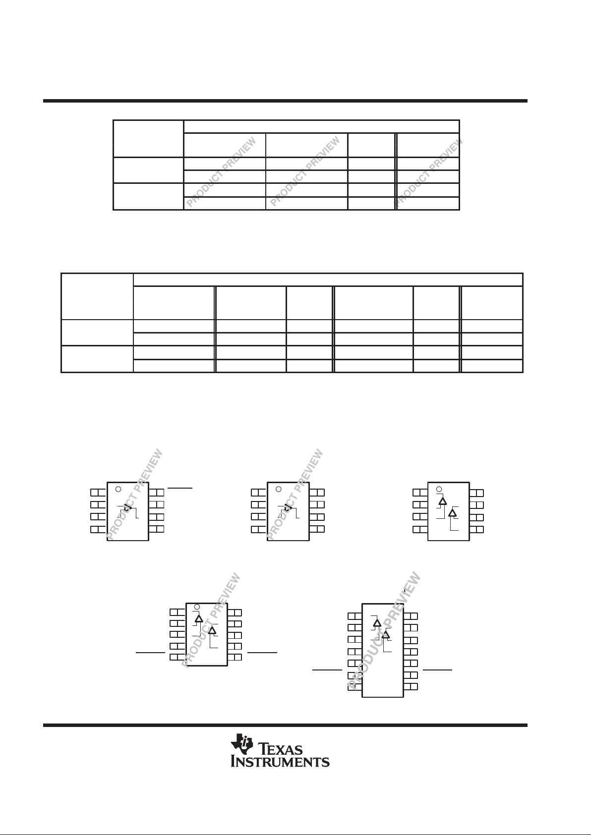
TLV4110 AND TLV4111 AVAILABLE OPTIONS
PACKAGED DEVICES
T
A
SMALL OUTLINE SMALL OUTLINE
PLASTIC DIP
(D)
†‡
(DGN)
†
SYMBOL
(P)
°
°
TLV4110CD TLV4110CDGN xxTIAHL TLV4110CP
0°C to 70°C
TLV4111CD TLV4111CDGN xxTIAHN TLV4111CP
°
°
TLV4110ID TLV4110IDGN xxTIAHM TLV4110IP
–
40°C to 125°C
TLV4111ID TLV4111IDGN xxTIAHO TLV4111IP
†
This package is available taped and reeled. T o order this packaging option, add an R suf fix to the part
number (e.g., TL V4110CDR).
‡
In the SOIC package, the maximum RMS output power is thermally limited to 350 mW; 700 mW peaks can be driven, as
long as the RMS value is less than 350 mW.
TLV4112 AND TLV4113 AVAILABLE OPTIONS
PACKAGED DEVICES
T
A
SMALL OUTLINE
SMALL OUT-
SMALL OUTLINE
PLASTIC DIP
(D)
†§
LINE
(DGN)
†
SYMBOL
(DGQ)
†
SYMBOL
(P)
°
°
TLV4112CD TLV4112DGN xxTIAHP — — TLV4112CP
0°C to 70°C
TLV4113CD
‡
— — TLV4113CDGN
‡
xxTIAHR TLV4113CN
‡
°
°
TLV4112ID TLV4112IDGN xxTIAHQ — — TLV4112IP
–
40°C to 125°C
TLV4113ID
‡
— — TLV4113IDGN
‡
xxTIAHS TLV4113IN
‡
†
This package is available taped and reeled. To order this packaging option, add an R suffix to the part number (e.g., TLV4112CDR).
‡
This device is in the Product Preview stage of development. Contact the local TI sales office for more information.
§
In the SOIC package, the maximum RMS output power is thermally limited to 350 mW; 700 mW peaks can be driven, as long as the
RMS value is less than 350 mW.
TLV411x PACKAGE PINOUTS
1
2
3
4
5
6
7
14
13
12
11
10
9
8
1OUT
1IN–
1IN+
GND
NC
1SHDN
NC
V
DD
2OUT
2IN–
2IN+
NC
2SHDN
NC
(TOP VIEW)
1
2
3
4
8
7
6
5
NC
IN–
IN+
GND
SHDN
NC
V
DD
OUT
TLV4110
D, DGN OR P PACKAGE
(TOP VIEW)
1
2
3
4
8
7
6
5
1OUT
1IN–
1IN+
GND
V
DD
2OUT
2IN–
2IN+
TLV4112
D, DGN, OR P PACKAGE
(TOP VIEW)
TLV4113
D OR N PACKAGE
NC – No internal connection
1
2
3
4
5
10
9
8
7
6
1OUT
1IN–
1IN+
GND
1SHDN
VDD+
2OUT
2IN–
2IN+
2SHDN
TLV4113
DGQ PACKAGE
(TOP VIEW)
1
2
3
4
8
7
6
5
NC
IN–
IN+
GND
NC
V
DD
OUT
NC
TLV4111
D, DGN OR P PACKAGE
(TOP VIEW)
TLV4110, TLV4111, TLV4112, TLV4113
FAMILY OF HIGH OUTPUT DRIVE OPERATIONAL
AMPLIFIERS WITH SHUTDOWN
SLOS289A – DECEMBER 1999 – REVISED APRIL 2000
3
POST OFFICE BOX 655303 • DALLAS, TEXAS 75265
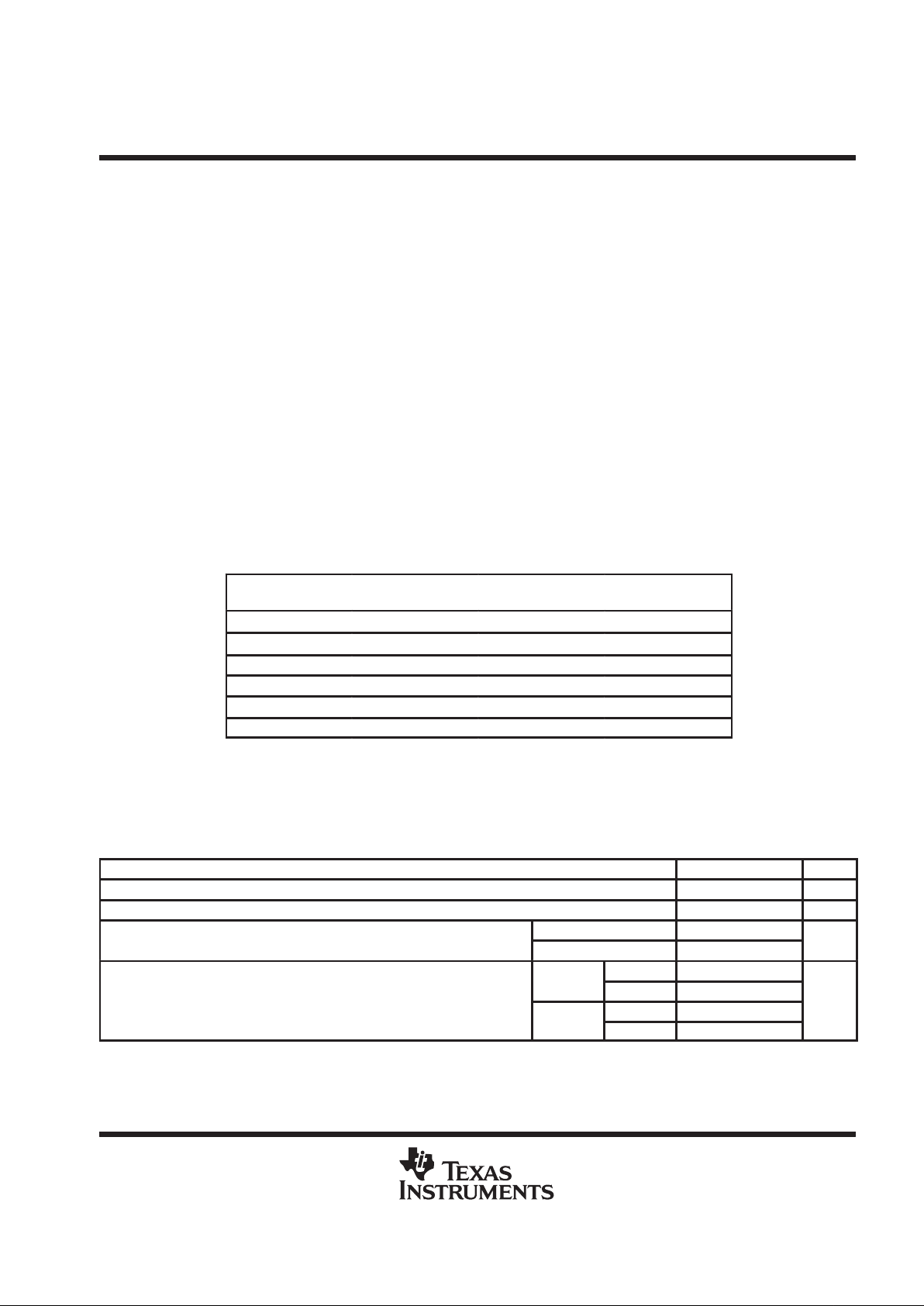
absolute maximum ratings over operating free-air temperature range (unless otherwise noted)
†
Supply voltage, VDD (see Note 1) 7 V. . . . . . . . . . . . . . . . . . . . . . . . . . . . . . . . . . . . . . . . . . . . . . . . . . . . . . . . . . . . .
Differential input voltage, VID ±V
DD
. . . . . . . . . . . . . . . . . . . . . . . . . . . . . . . . . . . . . . . . . . . . . . . . . . . . . . . . . . . . . .
Input voltage range, V
I
±V
DD
. . . . . . . . . . . . . . . . . . . . . . . . . . . . . . . . . . . . . . . . . . . . . . . . . . . . . . . . . . . . . . . . . . . .
Output current,IO (see Note 2) 800 mA. . . . . . . . . . . . . . . . . . . . . . . . . . . . . . . . . . . . . . . . . . . . . . . . . . . . . . . . . . . .
Continuous /RMS output current, IO (each output of amplifier): TJ ≤ 105°C 350 mA. . . . . . . . . . . . . . . . . . . .
TJ ≤ 150°C 110 mA. . . . . . . . . . . . . . . . . . . .
Peak output current, IO (each output of amplifier: TJ ≤ 105°C 500 mA. . . . . . . . . . . . . . . . . . . . . . . . . . . . . . . .
T
J
≤ 150°C 155 mA. . . . . . . . . . . . . . . . . . . . . . . . . . . . . . . .
Continuous total power dissipation See Dissipation Rating Table. . . . . . . . . . . . . . . . . . . . . . . . . . . . . . . . . . . . .
Operating free-air temperature range, TA: C suffix 0°C to 70°C. . . . . . . . . . . . . . . . . . . . . . . . . . . . . . . . . . . . . .
I suffix –40°C to 125°C. . . . . . . . . . . . . . . . . . . . . . . . . . . . . . . . . . . .
Maximum junction temperature, T
J
150°C. . . . . . . . . . . . . . . . . . . . . . . . . . . . . . . . . . . . . . . . . . . . . . . . . . . . . . . . .
Storage temperature range, T
stg
–65°C to 150°C. . . . . . . . . . . . . . . . . . . . . . . . . . . . . . . . . . . . . . . . . . . . . . . . . . .
Lead temperature 1,6 mm (1/16 inch) from case for 10 seconds 260°C. . . . . . . . . . . . . . . . . . . . . . . . . . . . . . .
†
Stresses beyond those listed under “absolute maximum ratings” may cause permanent damage to the device. These are stress ratings only, and
functional operation of the device at these or any other conditions beyond those indicated under “recommended operating conditions” is not
implied. Exposure to absolute-maximum-rated conditions for extended periods may affect device reliability.
NOTES: 1. All voltage values, except differential voltages, are with respect to GND.
2. To prevent permanent damage the die temperature must not exceed the maximum junction temperature.
DISSIPATION RATING TABLE
PACKAGE
θ
JC
(°C/W)
θ
JA
(°C/W)
TA ≤ 25°C
POWER RATING
D (8) 38.3 176 710 mW
D (14) 26.9 122.3 1022 mW
DGN (8)
‡
4.7 52.7 2.37 W
DGQ (10)
‡
4.7 52.3 2.39 W
P (8) 41 104 1200 mW
N (14) 32 78 1600 mW
‡
See The Texas Instruments document,
PowerPAD Thermally Enhanced Package Application
Report
(literature number SLMA002), for more information on the PowerPAD package. The
thermal data was measured on a PCB layout based on the information in the section entitled
Texas Instruments Recommended Board for PowerPAD
on page 33 of the before mentioned
document.
recommended operating conditions
MIN MAX UNIT
Supply voltage, V
DD
2.5 6 V
Common-mode input voltage range, V
ICR
0 VDD–1.5 V
p
p
C-suffix 0 70
°
Operating free-air temperature, T
A
I-suffix –40 125
°C
VDD = 3 V 2.1
V(on)
VDD = 5 V 3.8
Shutdown turn on/off voltage level
§
VDD = 3 V 0.9
V
V(off)
VDD = 5 V 1.65
§
Relative to GND
TLV4110, TLV4111, TLV4112, TLV4113
FAMILY OF HIGH OUTPUT DRIVE OPERATIONAL
AMPLIFIERS WITH SHUTDOWN
SLOS289A – DECEMBER 1999 – REVISED APRIL 2000
4
POST OFFICE BOX 655303 • DALLAS, TEXAS 75265
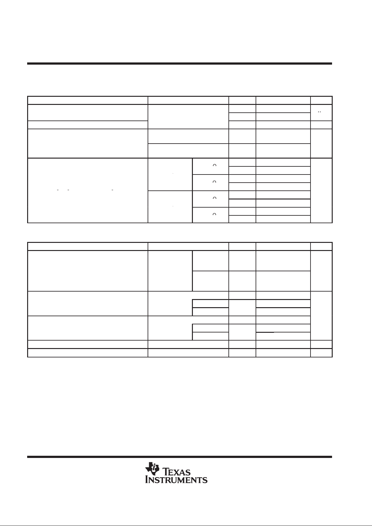
electrical characteristics at recommend operating conditions, VDD = 3 V and 5 V (unless otherwise
noted)
dc performance
PARAMETER TEST CONDITIONS T
A
†
MIN TYP MAX UNITS
p
25°C 175 3500
VIOInput offset voltage
VIC = VDD/2,
VO = VDD/2 ,
Full range 4000
µ
V
αVIO Offset voltage draft
R
L
=
100 Ω
,
R
S
= 50
Ω
25°C 3 µV/°C
VDD = 3 V,
RS = 50 Ω
VIC = 0 to 2 V,
25°C 63
CMRR
Common-mode rejection ratio
VDD = 5 V,
RS = 50 Ω
VIC = 0 to 4 V,
25°C 68
dB
25°C 78 84
V
= 3 V,
R
L
=
100 Ω
Full range 67
DD
,
V
O(PP)
=0 to 1V
25°C 85 100
Large-signal differential voltage
R
L
=10
kΩ
Full range 75
A
VD
gg g
amplification
25°C 88 94
dB
V
= 5 V,
R
L
=
100 Ω
Full range 75
DD
,
V
O(PP)
=0 to 3V
25°C 90 110
R
L
=
10 kΩ
Full range 85
†
Full range is 0°C to 70°C for C suffix and –40°C to 125°C for I suffix. If not specified, full range is –40°C to 125°C.
input characteristics
PARAMETER TEST CONDITIONS T
A
†
MIN TYP MAX UNITS
p
Measured over
VDD = 3 V
25°C and
Full range
0
to
1.5
V
ICR
Common-mode input voltage range
CMRR
range,
RS = 50 Ω
VDD = 5 V
25°C and
Full range
0
to
3.5
V
25°C 0.3 25
I
IO
Input offset current VIC = VDD/2
TLV411xC
50
TLV411xI
Full range
250
p
25°C 0.3 50
pA
I
IB
Input bias current
VO = VDD/2,
TLV411xC
100
R
S
= 50
Ω
TLV411xI
Full range
500
r
i(d)
Differential input resistance 25°C 1000 GΩ
C
IC
Common-mode input capacitance f = 100 Hz 25°C 5 pF
†
Full range is 0°C to 70°C for C suffix and –40°C to 125°C for I suffix. If not specified, full range is –40°C to 125°C.
TLV4110, TLV4111, TLV4112, TLV4113
FAMILY OF HIGH OUTPUT DRIVE OPERATIONAL
AMPLIFIERS WITH SHUTDOWN
SLOS289A – DECEMBER 1999 – REVISED APRIL 2000
5
POST OFFICE BOX 655303 • DALLAS, TEXAS 75265
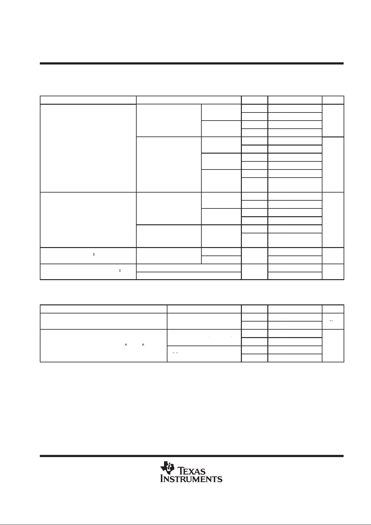
electrical characteristics at specified free-air temperature, VDD = 3 V and 5 V (unless otherwise
noted) (continued)
output characteristics
PARAMETER TEST CONDITIONS T
A
†
MIN TYP MAX UNITS
25°C 2.7 2.97
I
OH
= –10
mA
Full range 2.7
V
DD
=
3 V
,
V
IC
=
VDD/2
25°C 2.6 2.73
V
I
OH
=–
100 mA
Full range 2.6
25°C 4.7 4.96
V
OH
High-level output voltage
I
OH
= –10
mA
Full range 4.7
25°C 4.6 4.76
VDD = 5 V, VIC = VDD/2
I
OH
= –
100 mA
Full range 4.6
V
25°C 4.45 4.6
IOH = –200 mA
–40°C to
85°C
4.35
25°C 0.03 0.1
V
= 3 V and 5 V,
I
OL
= 10
mA
Full range 0.1
DD
,
VIC = VDD/2
25°C 0.33 0.4
V
OL
Low–level output voltage
I
OL
=
100 mA
Full range 0.55
V
25°C 0.38 0.6
VDD = 5 V, VIC = VDD/2 IOL = 200 mA
–40°C to
85°C
0.7
p
VDD = 3 V
°
±220
IOOutput current
‡
Measured at 0.5 V from rail
VDD = 5 V
25°C
±320
mA
p
Sourcing
°
800
IOSShort-circuit output current
‡
Sinking
25°C
800
mA
†
Full range is 0°C to 70°C for C suffix and –40°C to 125°C for I suffix. If not specified, full range is –40°C to 125°C.
‡
When driving output currents in excess of 200 mA, the MSOP PowerPAD package is required for thermal dissipation.
power supply
PARAMETER TEST CONDITIONS T
A
MIN TYP MAX UNITS
pp
p
25°C 700 1000
IDDSupply current (per channel)
V
O
=
VDD/2
Full range 1500
µ
A
V
=2.7 to 3.3 V , No load,
25°C 70 82
pp
DD
,
VIC = VDD/2 V
,
Full range 65
K
SVR
Power supply rejection ratio (∆V
DD
/
∆VIO)
VDD =4.5 to 5.5 V , No load,
25°C 70 79
dB
DD
VIC = VDD/2 V
Full range 65
†
Full range is 0°C to 70°C for C suffix and –40°C to 125°C for I suffix. If not specified, full range is –40°C to 125°C.
TLV4110, TLV4111, TLV4112, TLV4113
FAMILY OF HIGH OUTPUT DRIVE OPERATIONAL
AMPLIFIERS WITH SHUTDOWN
SLOS289A – DECEMBER 1999 – REVISED APRIL 2000
6
POST OFFICE BOX 655303 • DALLAS, TEXAS 75265
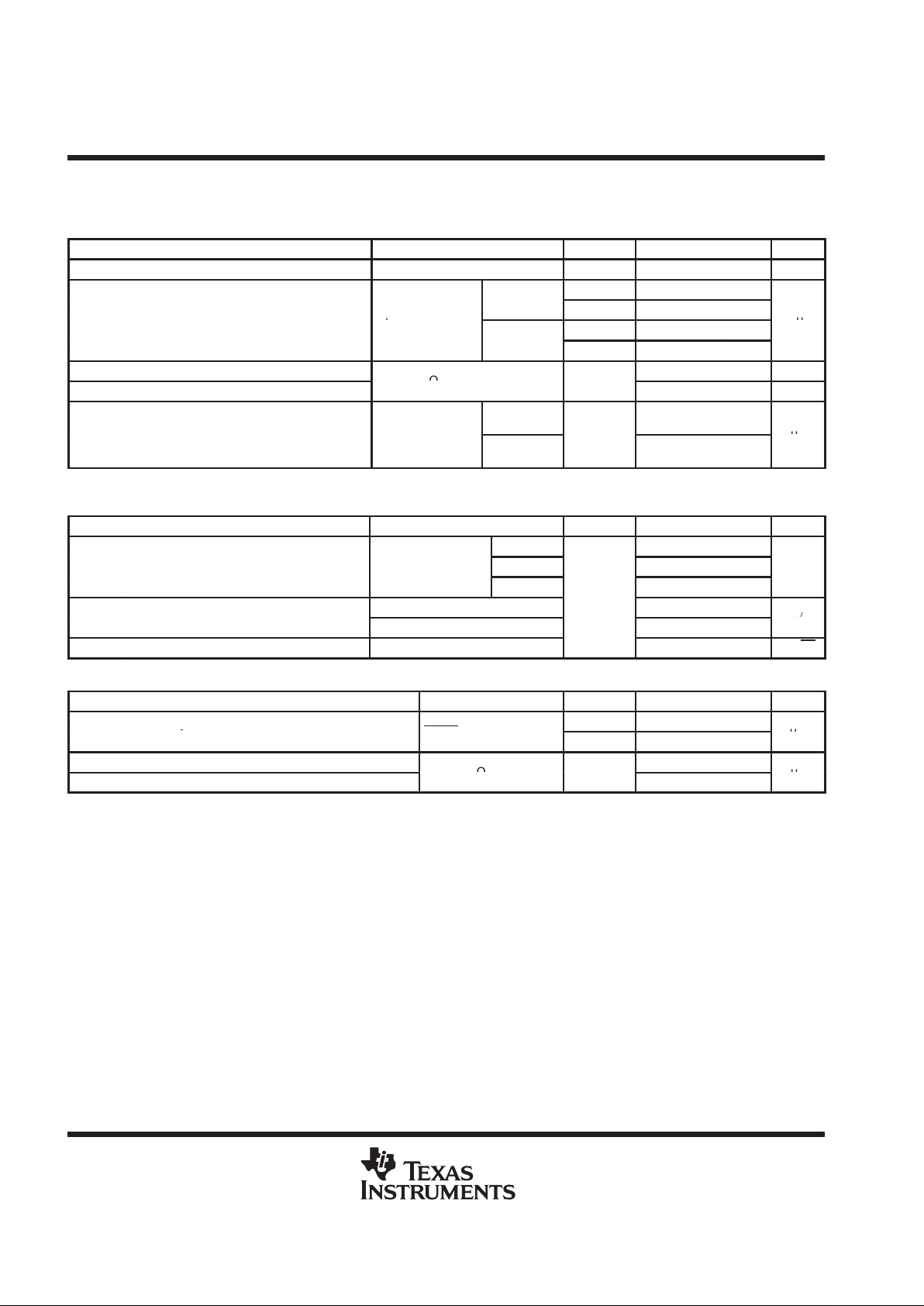
electrical characteristics at specified free-air temperature, VDD = 3 V and 5 V (unless otherwise
noted) (continued)
dynamic performance
PARAMETER TEST CONDITIONS T
A
†
MIN TYP MAX UNITS
GBWP Gain bandwidth product RL=100 Ω CL=10 pF 25°C 2.7 MHz
25°C 0.8 1.57
V
o(pp)
= 2 V,
V
DD
= 3
V
Full range 0.55
SR
Slew rate at unity gain
R
L
=
100 Ω
,
C
= 10 pF
25°C 1 1.57
V/µs
C
L
= 10
F
V
DD
= 5
V
Full range 0.7
φM Phase margin
p
°
66
Gain margin
R
L
=
100 Ω
,
C
L
=
10 pF
25°C
16 dB
V
(STEP)pp
= 1 V,
AV = –1,
0.1%
°
0.7
tsSettling time
V
CL = 10 pF,
RL = 100 Ω
0.01%
25°C
1.3
µ
s
†
Full range is 0°C to 70°C for C suffix and –40°C to 125°C for I suffix. If not specified, full range is –40°C to 125°C.
noise/distortion performance
PARAMETER TEST CONDITIONS T
A
MIN TYP MAX UNITS
pp
=
A
V
= 1 0.025
THD+N Total harmonic distortion plus noise
V
O( )
=
VDD/2 V
,
RL = 100 Ω,
AV = 10 0.035
f = 100 Hz
AV = 100
°
0.15
p
f = 100 Hz
25°C
55
VnEquivalent input noise voltage
f = 10 kHz 10
n
V/√H
z
I
n
Equivalent input noise current f = 1 kHz 0.31 fA/√Hz
shutdown characteristics
PARAMETER TEST CONDITIONS T
A
†
MIN TYP MAX UNITS
Supply current in shutdown mode (per channel)
25°C TBD
I
DD(SHDN)
y()
(TLV4110, TLV41 13)
SHDN
= 0
V
Full range TBD
µ
A
t
(ON)
Amplifier turnon time
‡
°
TBD
t
(Off)
Amplifier turnoff time
‡
R
L
=
100 Ω
25°C
TBD
µ
s
†
Full range is 0°C to 70°C for C suffix and –40°C to 125°C for I suffix. If not specified, full range is –40°C to 125°C.
‡
Disable time and enable time are defined as the interval between application of the logic signal to SHDN and the point at which the supply current
has reached half its final value.
TLV4110, TLV4111, TLV4112, TLV4113
FAMILY OF HIGH OUTPUT DRIVE OPERATIONAL
AMPLIFIERS WITH SHUTDOWN
SLOS289A – DECEMBER 1999 – REVISED APRIL 2000
7
POST OFFICE BOX 655303 • DALLAS, TEXAS 75265
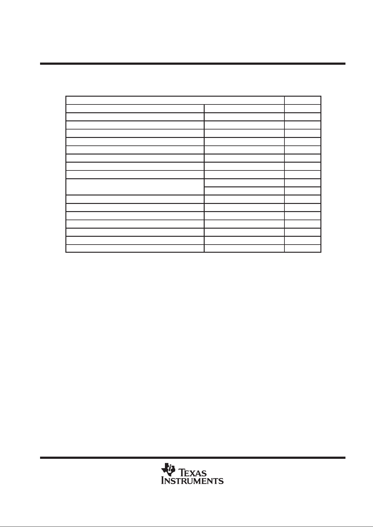
TYPICAL CHARACTERISTICS
Table of Graphs
FIGURE
V
IO
Input offset voltage vs Common-mode input voltage 1, 2
CMRR Common-mode rejection ratio vs Frequency 3
V
OH
High-level output voltage vs High-level output current 4, 6
V
OL
Low-level output voltage vs Low-level output current 5, 7
Z
o
Output impedance vs Frequency 8
I
DD
Supply current vs Supply voltage 9
k
SVR
Supply voltage rejection ratio vs Frequency 10
A
VD
Differential voltage amplification and phase vs Frequency 11
Gain-bandwidth product vs Supply voltage 12
vs Supply voltage 13
SR
Slew rate
vs Temperature 14
T otal harmonic distortion+noise vs Frequency 15
V
n
Equivalent input voltage noise vs Frequency 16
Phase margin vs Capacitive load 17
Voltage-follower signal pulse response vs Time 18, 19
Inverting large-signal pulse response vs Time 20, 21
Small-signal inverting pulse response vs Time 22
Crosstalk vs Frequency 23
 Loading...