

Page 1
TLV320DAC3120
www.ti.com
Low-Power Mono Audio DAC With Embedded miniDSP
and Mono Class-D Speaker Amplifier
Check for Samples: TLV320DAC3120
1 INTRODUCTION
1.1 Features 1.2 Applications
1
• Mono Audio DAC With 95-dB SNR
• Instruction-Programmable Embedded miniDSP
• Supports 8-kHz to 192-kHz Sample Rates
• Mono Class-D BTL Speaker Driver (2.5 W Into
4 Ω or 1.6 W Into 8 Ω)
• Mono Headphone/Lineout Driver
• Two Single-Ended Inputs With Output Mixing
and Level Control
• Microphone Bias
• Built-in Digital Audio Processing Blocks With
User-Programmable Biquad, FIR Filters, and
DRC
• Programmable Digital Audio Processor for
Bass Boost/Treble/EQ With up to Six Biquads
for Playback
• Pin Control or Register Control for Digital
Playback Volume-Control Settings
• Integrated PLL Used for Programmable Digital
Audio Processor
• I2S, Left-Justified, Right-Justified, DSP, and
TDM Audio Interfaces
• I2C Control With Register Auto-Increment
• Full Power-Down Control
• Power Supplies:
– Analog: 2.7 V–3.6 V
– Digital Core: 1.65 V–1.95 V
– Digital I/O: 1.1 V–3.6 V
– Class-D: 2.7 V–5.5 V (SPKVDD ≥ AVDD)
• 5-mm × 5-mm 32-QFN Package
• Portable Audio Devices
• eBook
• Portable Navigation Devices
1.3 Description
The TLV320DAC3120 is a low-power, highly
integrated, high-performance mono DAC with 24-bit
mono playback.
The device integrates several analog features, such
as a microphone bias, headphone drivers, and a
mono speaker driver capable of driving a 4-Ω load.
The TLV320DAC3120 has a fully programmable
miniDSP for digital audio processing. The digital
audio data format is programmable to work with
popular audio standard protocols (I2S,
left/right-justified) in master, slave, DSP, and TDM
modes. Bass boost, treble, or EQ can be supported
by the programmable digital-signal processing block.
An on-chip PLL provides the high-speed clock
needed by the digital signal-processing block. The
volume level can be controlled by either a pin control
or by register control. The audio functions are
controlled using the I2C serial bus.
The TLV320DAC3120 is available in a 32-pin QFN
package.
SLAS659–NOVEMBER 2009
1
Please be aware that an important notice concerning availability, standard warranty, and use in critical applications of Texas
Instruments semiconductor products and disclaimers thereto appears at the end of this data sheet.
PRODUCTION DATA information is current as of publication date.
Products conform to specifications per the terms of the Texas
Instruments standard warranty. Production processing does not
necessarily include testingof all parameters.
Copyright © 2009, Texas Instruments Incorporated
Page 2
Digital
Audio
Processing
and
Serial
Interface
SDIN
BCLK
WCLK
MCLK PLL
HPVDDHPVSS
SPKVDDSPKVSS
AVDDAVSS
SPKVSS
SPKVDD
VOL/MICDET
SCL
SDA
GPIOGPIO1
DAC
MIXER
P1/R35
RESET
DVDDDVSS
IOVDD
IOVSS
AIN2
AIN1
2 V/2.5 V/AVDD
MICBIAS
Note: Normally,
MCLK is PLL input;
however, BCLK or
GPIO1 can also be
PLL input.
Audio Output Stage
Power Management
De-Pop
and
Soft Start
RC CLK
P1/R33–R34
P1/R46
I C
2
Mono DAC
SPKP
SPKM
Class-D Speaker
Driver
6 dB to 24 dB
(6-dB steps)
Analog
Attenuation
0 dB to –78 dB
and Mute
(0.5-dB steps)
P1/R42
P1/R38
SPKP
SPKM
Class A/B
Headphone/Lineout
Driver
0 dB to 9 dB
(1-dB steps)
Analog
Attenuation
HPOUT
P1/R36
P1/R40
P1/R30–R31
L Data
R Data
(L+R)/2 Data
P0/R63
7-Bit ADC P0/R116
Left and Right
Volume-Control Register
P0/R117
Digital Vol
24 dB to
Mute
miniDSP
P0/R64
S
0 dB to –78 dB
and Mute
(0.5-dB steps)
B0360-01
TLV320DAC3120
SLAS659–NOVEMBER 2009
This integrated circuit can be damaged by ESD. Texas Instruments recommends that all integrated circuits be handled with
appropriate precautions. Failure to observe proper handling and installation procedures can cause damage.
ESD damage can range from subtle performance degradation to complete device failure. Precision integrated circuits may be more
susceptible to damage because very small parametric changes could cause the device not to meet its published specifications.
www.ti.com
This data manual is designed using PDF document-viewing features that allow quick
access to information. For example, performing a global search on "page 0 / register 27"
produces all references to this page and register in a list. This makes is easy to traverse
the list and find all information related to a page and register. Note that the search string
must be of the indicated format. Also, this document includes document hyperlinks to
allow the user to quickly find a document reference. To come back to the original page,
click the green left arrow near the PDF page number at the bottom of the file. The hot-key
for this function is alt-left arrow on the keyboard. Another way to find information quickly is
to use the PDF bookmarks.
Figure 1-1. Functional Block Diagram
NOTE
2 INTRODUCTION Copyright © 2009, Texas Instruments Incorporated
Submit Documentation Feedback
Product Folder Link(s): TLV320DAC3120
Page 3
P0048-12
AVSSSPKVSS
IOVSS
SPKVDD
24123222321420519618717
8
16
25
15
26
14
27
13
28
12
29
1130
1031
932
NC
SPKM
AIN2
SPKP
AIN1
SPKVDD
MICBIAS
SPKVSS
VOL/MICDET
SPKM
SCL
DVSS
SDA
AVDD
RHB Package
(Top View)
SPKP
IOVDD
HPOUT
DVDD
HPVDD
NC
HPVSS
DIN
NC
WCLK
RESET
BCLK
GPIO1
MCLK
TLV320DAC3120
TLV320DAC3120
www.ti.com
SLAS659–NOVEMBER 2009
2 PACKAGE AND SIGNAL DESCRIPTIONS
2.1 Package/Ordering Information
PRODUCT PACKAGE TEMPERATURE ORDERING NUMBER QUANTITY
PACKAGE
DESIGNATOR
TLV320DAC3120 QFN-32 RHB –40°C to 85°C
2.2 Device Information
OPERATING TRANSPORT MEDIA,
RANGE
TLV320DAC3120IRHBT Tape and reel, 250
TLV320DAC3120IRHBR Tape and reel, 3000
Table 2-1. TERMINAL FUNCTIONS
TERMINAL
NAME NO.
AIN1 13 I Analog input #1 routed to output mixer
AIN2 14 I Analog input #2 routed to output mixer
AVDD 17 – Analog power supply
AVSS 16 – Analog ground
BCLK 7 I/O Audio serial bit clock
DIN 5 I Audio serial data input
DVDD 3 – Digital power – digital core
DVSS 18 – Digital ground
GPIO1 32 I/O General-purpose input/output and multifunction pin
HPOUT 27 O Headphone/lineout driver output
HPVDD 28 – Headphone/line driver and PLL power
HPVSS 29 – Headphone/line driver and PLL ground
IOVDD 2 – Interface power
IOVSS 1 – Interface ground
MCLK 8 I Exterrnal master clock
Copyright © 2009, Texas Instruments Incorporated PACKAGE AND SIGNAL DESCRIPTIONS 3
I/O DESCRIPTION
Submit Documentation Feedback
Product Folder Link(s): TLV320DAC3120
Page 4
TLV320DAC3120
SLAS659–NOVEMBER 2009
www.ti.com
TERMINAL FUNCTIONS (continued)
TERMINAL
NAME NO.
MICBIAS 12 O Micophone bias voltage
NC 4, 15, 30 – No connection
RESET 31 I Device reset
SCL 10 I/O I2C control-bus clock input
SDA 9 I/O I2C control-bus data input
SPKM 19, 23 O Class-D speaker driver inverting output
SPKP 22, 26 O Class-D speaker driver noninverting output
SPKVDD 21, 24 – Class-D speaker driver power supply
SPKVSS 20, 25 – Class-D speaker driver power-supply ground
VOL/MICDET 11 I Volume control or microphone/headphone/headset detection
WCLK 6 I/O Audio serial word clock
I/O DESCRIPTION
3 ELECTRICAL SPECIFICATIONS
3.1 Absolute Maximum Ratings
over operating free-air temperature range (unless otherwise noted)
AVDD to AVSS –0.3 to 3.9 V
DVDD to DVSS –0.3 to 2.5 V
HPVDD to HPVSS –0.3 to 3.9 V
SPKVDD to SPKVSS –0.3 to 6 V
IOVDD to IOVSS –0.3 to 3.9 V
Digital input voltage IOVSS – 0.3 to IOVDD + 0.3 V
Analog input voltage AVSS – 0.3 to AVDD + 0.3 V
Operating temperature range –40 to 85 °C
Storage temperature range –55 to 150 °C
Junction temperature (TJMax) 105 °C
QFN package
(1) Stresses beyond those listed under Absolute Maximum Ratings may cause permanent damage to the device. These are stress ratings
only, and functional operation of the device at these or any other conditions beyond those indicated under Recommended Operating
Conditions is not implied. Exposure to absolute-maximum-rated conditions for extended periods may affect device reliability.
Power dissipation (TJMax – TA)/R
R
Thermal impedance (with thermal pad soldered to board) 35 °C/W
θJA
(1)
VALUE UNIT
θJA
W
Table 3-1. System Thermal Characteristics
Power Rating at 25°C Derating Factor Power Rating at 70°C Power Rating at 85°C
2.3 W 28.57 mW/°C 1 W 0.6 W
(1) This data was taken using 2-oz. (0.071-mm thick) trace and copper pad that is soldered to a JEDEC high-K, standard 4-layer
3-in. × 3-in. (7.62-cm × 7.62-cm) PCB.
4 ELECTRICAL SPECIFICATIONS Copyright © 2009, Texas Instruments Incorporated
Submit Documentation Feedback
Product Folder Link(s): TLV320DAC3120
(1)
Page 5
TLV320DAC3120
www.ti.com
SLAS659–NOVEMBER 2009
3.2 Recommended Operating Conditions
over operating free-air temperature range (unless otherwise noted)
MIN NOM MAX UNIT
(1)
AVDD
Referenced to AVSS
DVDD Referenced to DVSS
HPVDD Power-supply voltage range Referenced to HPVSS
SPKVDD
(1)
Referenced to SPKVSS
IOVDD Referenced to IOVSS
Speaker impedance Load applied across class-D output pins (BTL) 4 Ω
Headphone impedance AC-coupled to R
V
I
MCLK
(3)
Analog audio full-scale input
voltage
Mono line output load
impedance
AVDD = 3.3 V, single-ended 0.707 V
AC-coupled to R
Master clock frequency IOVDD = 3.3 V 50 MHz
SCL SCL clock frequency 400 kHz
T
A
Operating free-air temperature –40 85 °C
(1) To minimize battery-current leakage, the SPKVDD and SPKVDD voltage levels should not be below the AVDD voltage level.
(2) All grounds on board are tied together, so they should not differ in voltage by more than 0.2 V maximum for any combination of ground
signals. By use of a wide trace or ground plane, ensure a low-impedance connection between HPVSS and DVSS.
(3) The maximum input frequency should be 50 MHz for any digital pin used as a general-purpose clock.
(2)
(2)
(2)
(2)
(2)
L
L
2.7 3.3 3.6
1.65 1.8 1.95
2.7 3.3 3.6
2.7 5.5
1.1 3.3 3.6
16 Ω
10 kΩ
V
RMS
3.3 Electrical Characteristics
At 25°C, AVDD = HPVDD = IOVDD = 3.3 V, SPKVDD = 3.6 V, DVDD = 1.8 V, fS(audio) = 48 kHz,
CODEC_CLKIN = 256 × fS, PLL = Off, VOL/MICDET pin disabled (unless otherwise noted)
PARAMETER TEST CONDITIONS MIN TYP MAX UNIT
INTERNAL OSCILLATOR—RC_CLK
Oscillator frequency 8.2 MHz
VOLUME CONTROL PIN (ADC); VOL/MICDET pin enabled
Input voltage range 0 / register 116, bit D7 = 1 and page 0 / register 67, 0 V
Input capacitance 2 pF
Volume control steps 128 Steps
MICROPHONE BIAS
Voltage output V
Voltage regulation mV
VOL/MICDET pin configured as volume control (page
bit D7 = 0)
Page 1 / register 46, bits D1–D0 = 10 2.25 2.5 2.75
Page 1 / register 46, bits D1–D0 = 01 2
At 4-mA load current, page 1 / register 46, bits D1–D0
= 10 (MICBIAS = 2.5 V)
At 4-mA load current, page 1 / register 46, bits D1–D0
= 01 (MICBIAS = 2 V)
0.5 ×
AVDD
5
7
Copyright © 2009, Texas Instruments Incorporated ELECTRICAL SPECIFICATIONS 5
Submit Documentation Feedback
Product Folder Link(s): TLV320DAC3120
Page 6
TLV320DAC3120
SLAS659–NOVEMBER 2009
www.ti.com
Electrical Characteristics (continued)
At 25°C, AVDD = HPVDD = IOVDD = 3.3 V, SPKVDD = 3.6 V, DVDD = 1.8 V, fS(audio) = 48 kHz,
CODEC_CLKIN = 256 × fS, PLL = Off, VOL/MICDET pin disabled (unless otherwise noted)
PARAMETER TEST CONDITIONS MIN TYP MAX UNIT
DAC HEADPHONE OUTPUT, AC-COUPLED LOAD = 16 Ω (SINGLE-ENDED),
DRIVER GAIN = 0 dB, PARASITIC CAPACITANCE = 30 pF
Full-scale output voltage
(0 dB)
SNR Signal-to-noise ratio Measured as idle-channel noise, A-weighted
THD Total harmonic distortion 0-dBFS input –85 –65 dB
THD+N 0-dBFS input –82 –60 dB
Total harmonic distortion +
noise
Mute attenuation 87 dB
PSRR Power-supply rejection ratio
P
O
Maximum output power mW
DAC LINEOUT (HP Driver in Lineout Mode)
SNR Signal-to-noise ratio Measured as idle-channel noise, A-weighted 95 dB
THD Total harmonic distortion 0-dBFS input, 0-dB gain –86 dB
THD+N 0-dBFS input, 0-dB gain –83 dB
Total harmonic distortion +
noise
DAC DIGITAL INTERPOLATION FILTER CHARACTERISTICS
See Section 5.6.1.4 for DAC interpolation filter characteristics.
DAC OUTPUT TO CLASS-D SPEAKER OUTPUT; LOAD = 4 Ω (DIFFERENTIAL), 50 pF
Output voltage Vrms
Output, common-mode 1.8 V
SNR Signal-to-noise ratio 6 dB, measured as idle-channel noise, A-weighted 88 dB
THD Total harmonic distortion –65 dB
THD+N –63 dB
Total harmonic distortion + SPKVDD = 3.6 V, BTL measurement, DAC input = –6
noise dBFS, CM = 1.8 V, class-D gain = 6 dB
PSRR Power-supply rejection ratio –44 dB
Mute attenuation 110 dB
P
O
Maximum output power 1.5 W
(1) Ratio of output level with 1-kHz full-scale sine-wave input, to the output level with the inputs short-circuited, measured A-weighted over a
20-Hz to 20-kHz bandwidth using an audio analyzer.
(2) All performance measurements done with 20-kHz low-pass filter and, where noted, A-weighted filter. Failure to use such a filter may
result in higher THD+N and lower SNR and dynamic range readings than shown in the Electrical Characteristics. The low-pass filter
removes out-of-band noise, which, although not audible, may affect dynamic specification values.
(3) DAC to headphone-out PSRR measurement is calculated as PSRR = 20 X log(∆V
Output common-mode setting = 1.65 V 0.707 Vrms
(1) (2)
(3)
Ripple on HPVDD (3.3 V) = 200 mVp-p at 1 kHz –62 dB
80 95 dB
RL= 32 Ω, THD+N ≤ –60 dB 20
RL= 16 Ω, THD+N ≤ –60 dB 60
SPKVDD = 3.6 V, BTL measurement, CM = 1.8 V,
DAC input = 0 dBFS, class-D gain = 6 dB, THD ≤ 2.3
–16.5 dB
SPKVDD = 3.6 V, BTL measurement, CM = 1.8 V,
DAC input = –2 dBFS, class-D gain = 6 dB, THD ≤ 2.1
–20 dB
SPKVDD = 3.6 V, BTL measurement, DAC input =
mute, CM = 1.8 V, class-D gain = 6 dB
SPKVDD = 3.6 V, BTL measurement, class-D gain =
(with respect to full-scale output value of 2.3 Vrms)
SPKVDD = 3.6 V, BTL measurement, DAC input = –6
dBFS, CM = 1.8 V, class-D gain = 6 dB
SPKVDD = 3.6 V, BTL measurement, ripple on
SPKVDD = 200 mVp-p at 1 kHz
SPKVDD = 3.6 V, BTL measurement, CM = 1.8 V,
class-D gain = 18 dB, THD = 10%
1
SPKVDD = 4.3 V, BTL measurement, CM = 1.8 V,
class-D gain = 18 dB, THD = 10%
SPKVDD = 5.5 V, BTL measurement, CM = 1.8 V,
class-D gain = 18 dB, THD = 10%
/ ∆V
HPL
HPVDD
).
2.5
6 ELECTRICAL SPECIFICATIONS Copyright © 2009, Texas Instruments Incorporated
Submit Documentation Feedback
Product Folder Link(s): TLV320DAC3120
Page 7
TLV320DAC3120
www.ti.com
SLAS659–NOVEMBER 2009
Electrical Characteristics (continued)
At 25°C, AVDD = HPVDD = IOVDD = 3.3 V, SPKVDD = 3.6 V, DVDD = 1.8 V, fS(audio) = 48 kHz,
CODEC_CLKIN = 256 × fS, PLL = Off, VOL/MICDET pin disabled (unless otherwise noted)
PARAMETER TEST CONDITIONS MIN TYP MAX UNIT
DAC OUTPUT TO CLASS-D SPEAKER OUTPUT; LOAD = 8 Ω (DIFFERENTIAL), 50 pF
SPKVDD = 3.6 V, BTL measurement, CM = 1.8 V,
DAC input = 0 dBFS, class-D gain = 6 dB, THD ≤ 2.2
Output voltage Vrms
Output, common-mode 1.8 V
SNR Signal-to-noise ratio 6 dB, measured as idle-channel noise, A-weighted 87 dB
THD Total harmonic distortion –67 dB
THD+N –66 dB
Total harmonic distortion + SPKVDD = 3.6 V, BTL measurement, DAC input = –6
noise dBFS, CM = 1.8 V, class-D gain = 6 dB
PSRR Power-supply rejection ratio
Mute attenuation 110 dB
P
O
Maximum output power 1 W
Output-stage leakage current SPKVDD = 4.3 V, device is powered down
for direct battery connection (power-up-reset condition)
DAC POWER CONSUMPTION
DAC power consumption based per selected processing block, see Section 5.4
(1) DAC to speaker-out PSRR is a differential measurement calculated as PSRR = 20 × log(∆V
–16.5 dB
SPKVDD = 3.6 V, BTL measurement, CM = 1.8 V,
DAC input = –2 dBFS, class-D gain = 6 dB, THD ≤ 2.1
–20 dB
SPKVDD = 3.6 V, BTL measurement, DAC input =
mute, CM = 1.8 V, class-D gain = 6 dB
SPKVDD = 3.6 V, BTL measurement, class-D gain =
(with respect to full-scale output value of 2.3 Vrms)
SPKVDD = 3.6 V, BTL measurement, DAC input = –6
dBFS, CM = 1.8 V, class-D gain = 6 dB
SPKVDD = 3.6 V, BTL measurement, ripple on
(1)
SPKVDD = 200 mVp-p at 1 kHz
SPKVDD = 3.6 V, BTL measurement, CM = 1.8 V,
class-D gain = 18 dB, THD = 10%
SPKVDD = 4.3 V, BTL measurement, CM = 1.8 V,
class-D gain = 18 dB, THD = 10%
SPKVDD = 5.5 V, BTL measurement, CM = 1.8 V,
class-D gain = 18 dB, THD = 10%
SPK(P + M)
/ ∆V
–44 dB
0.7
1.6
80 nA
).
SPKVDD
Copyright © 2009, Texas Instruments Incorporated ELECTRICAL SPECIFICATIONS 7
Submit Documentation Feedback
Product Folder Link(s): TLV320DAC3120
Page 8
T0145-10
WCLK
BCLK
DIN
t (WS)
d
t (DI)
S
t (DI)
h
t
r
t
f
TLV320DAC3120
SLAS659–NOVEMBER 2009
Electrical Characteristics (continued)
At 25°C, AVDD = HPVDD = IOVDD = 3.3 V, SPKVDD = 3.6 V, DVDD = 1.8 V, fS(audio) = 48 kHz,
CODEC_CLKIN = 256 × fS, PLL = Off, VOL/MICDET pin disabled (unless otherwise noted)
PARAMETER TEST CONDITIONS MIN TYP MAX UNIT
DIGITAL INPUT/OUTPUT
Logic family CMOS
V
IH
IIH= 5 μA, IOVDD ≥ 1.6 V
IIH= 5 μA, IOVDD < 1.6 V IOVDD
V
IL
V
OH
V
OL
Logic level
IIL= 5 μA, IOVDD ≥ 1.6 V –0.3
IIL= 5 μA, IOVDD < 1.6 V 0
IOH= 2 TTL loads V
IOL= 2 TTL loads V
Capacitive load 10 pF
0.7 ×
IOVDD
0.8 ×
IOVDD
3.4 Timing Characteristics
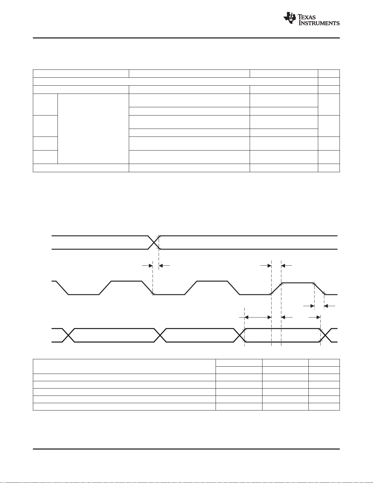
3.4.1 I2S/LJF/RJF Timing in Master Mode
0.3 ×
IOVDD
0.1 ×
IOVDD
www.ti.com
V
V
All specifications at 25°C, DVDD = 1.8 V
Note: All timing specifications are measured at characterization but not tested at final test.
PARAMETER IOVDD = 1.1 V IOVDD = 3.3 V UNIT
MIN MAX MIN MAX
td(WS) WCLK delay 45 20 ns
ts(DI) DIN setup 8 6 ns
th(DI) DIN hold 8 6 ns
t
r
t
f
Rise time 25 10 ns
Fall time 25 10 ns
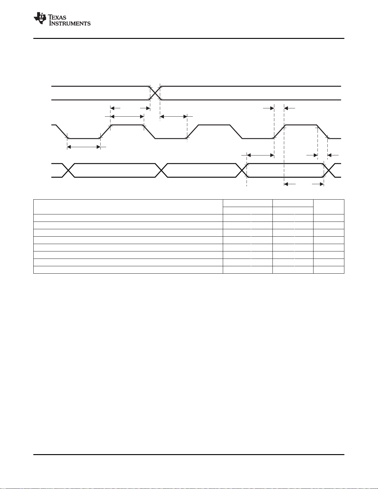
Figure 3-1. I2S/LJF/RJF Timing in Master Mode
8 ELECTRICAL SPECIFICATIONS Copyright © 2009, Texas Instruments Incorporated
Submit Documentation Feedback
Product Folder Link(s): TLV320DAC3120
Page 9
T0145-11
WCLK
BCLK
DIN
t (WS)
h
t (BCLK)
H
t (DI)
S
t (BCLK)
L
t (DI)
h
t (WS)
S
t
r
t
f
TLV320DAC3120
www.ti.com
SLAS659–NOVEMBER 2009
3.4.2 I2S/LJF/RJF Timing in Slave Mode
All specifications at 25°C, DVDD = 1.8 V
Note: All timing specifications are measured at characterization but not tested at final test.
PARAMETER UNIT
tH(BCLK) BCLK high period 35 35 ns
tL(BCLK) BCLK low period 35 35 ns
ts(WS) WCLK setup 8 6 ns
th(WS) WCLK hold 8 6 ns
ts(DI) DIN setup 8 6 ns
th(DI) DIN hold 8 6 ns
t
r
t
f
Rise time 4 4 ns
Fall time 4 4 ns
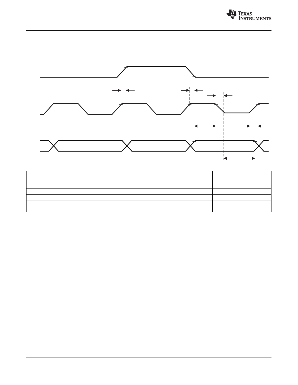
Figure 3-2. I2S/LJF/RJF Timing in Slave Mode
IOVDD = 1.1 V IOVDD = 3.3 V
MIN MAX MIN MAX
Copyright © 2009, Texas Instruments Incorporated ELECTRICAL SPECIFICATIONS 9
Submit Documentation Feedback
Product Folder Link(s): TLV320DAC3120
Page 10
T0146-09
WCLK
BCLK
DIN
t (WS)
d
t (WS)
d
t (DI)
S
t (DI)
h
t
f
t
r
TLV320DAC3120
SLAS659–NOVEMBER 2009
3.4.3 DSP Timing in Master Mode
All specifications at 25°C, DVDD = 1.8 V
Note: All timing specifications are measured at characterization but not tested at final test.
www.ti.com
PARAMETER UNIT
IOVDD = 1.1 V IOVDD = 3.3 V
MIN MAX MIN MAX
td(WS) WCLK delay 45 20 ns
ts(DI) DIN setup 8 8 ns
th(DI) DIN hold 8 8 ns
t
r
t
f
Rise time 25 10 ns
Fall time 25 10 ns
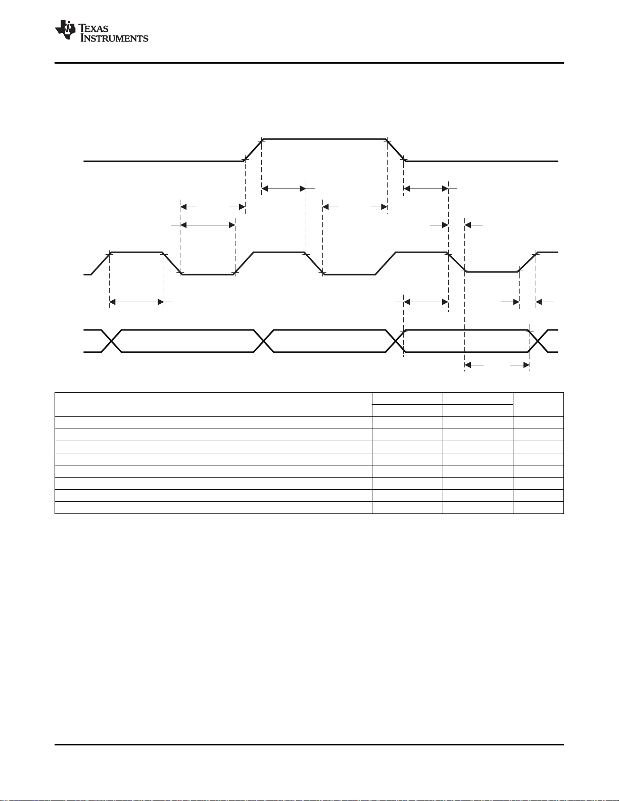
Figure 3-3. DSP Timing in Master Mode
10 ELECTRICAL SPECIFICATIONS Copyright © 2009, Texas Instruments Incorporated
Submit Documentation Feedback
Product Folder Link(s): TLV320DAC3120
Page 11
T0146-10
WCLK
BCLK
DIN
t (WS)
h
t (WS)
h
t (BCLK)
L
t
r
t
f
t (DI)
S
t (BCLK)
H
t (DI)
h
t (WS)
S
t (WS)
S
TLV320DAC3120
www.ti.com
3.4.4 DSP Timing in Slave Mode
All specifications at 25°C, DVDD = 1.8 V
Note: All timing specifications are measured at characterization but not tested at final test.
SLAS659–NOVEMBER 2009
PARAMETER UNIT
IOVDD = 1.1 V IOVDD = 3.3 V
MIN MAX MIN MAX
tH(BCLK) BCLK high period 35 35 ns
tL(BCLK) BCLK low period 35 35 ns
ts(WS) WCLK setup 8 8 ns
th(WS) WCLK hold 8 8 ns
ts(DI) DIN setup 8 8 ns
th(DI) DIN hold 8 8 ns
t
r
t
f
Rise time 4 4 ns
Fall time 4 4 ns
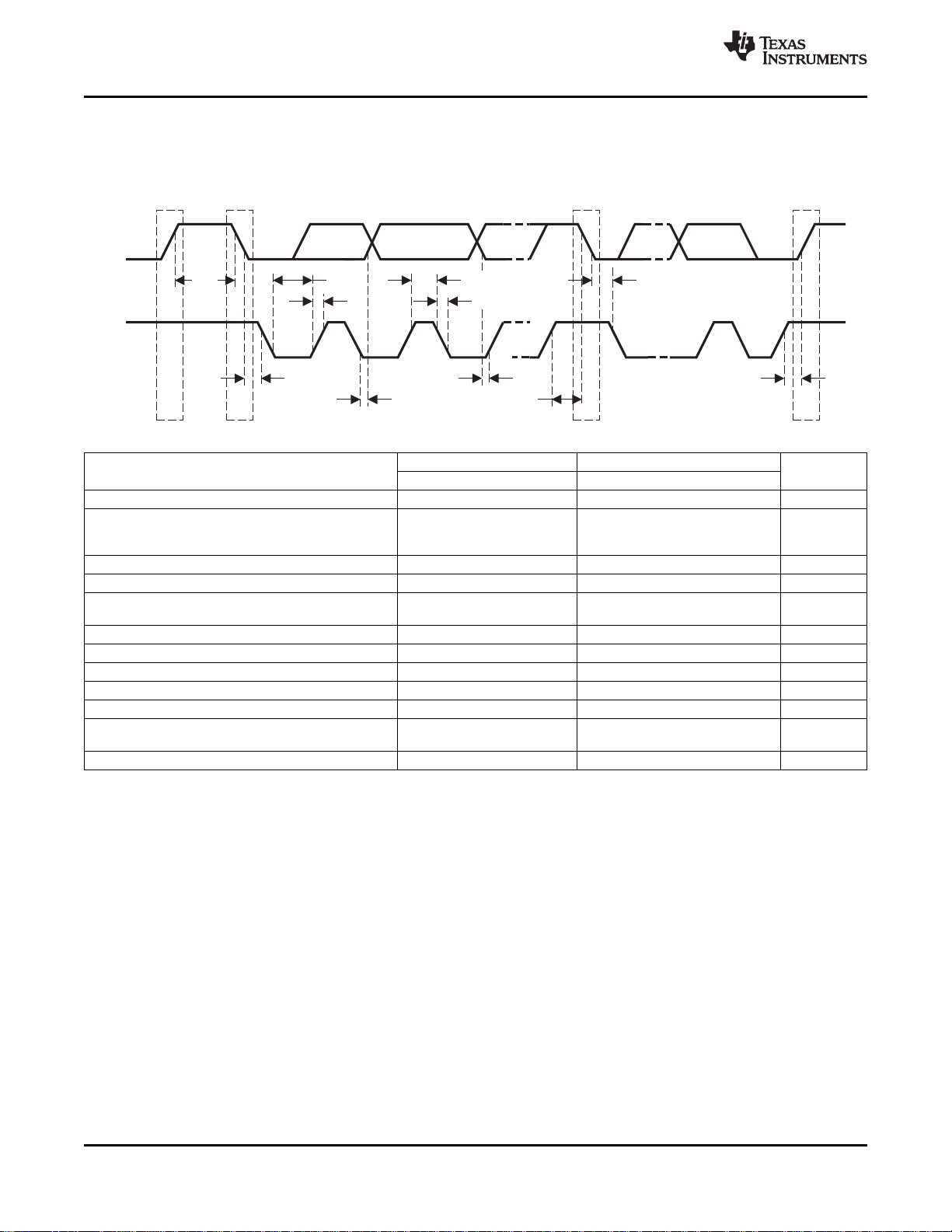
Figure 3-4. DSP Timing in Slave Mode
Copyright © 2009, Texas Instruments Incorporated ELECTRICAL SPECIFICATIONS 11
Submit Documentation Feedback
Product Folder Link(s): TLV320DAC3120
Page 12
STO
STA STA
STO
SDA
SCL
t
BUF
t
LOW
t
SU;STA
t
HIGH
t
HD;STA
t
r
t
HD;STA
t
HD;DAT
t
SU;DAT
t
SU;STO
t
f
T0295-02
TLV320DAC3120
SLAS659–NOVEMBER 2009
3.4.5 I2C Interface Timing
All specifications at 25°C, DVDD = 1.8 V
Note: All timing specifications are measured at characterization but not tested at final test.
PARAMETER Standard-Mode Fast-Mode UNITS
MIN TYP MAX MIN TYP MAX
f
SCL
t
HD;STA
t
LOW
t
HIGH
t
SU;STA
t
HD;DAT
t
SU;DAT
t
r
t
f
t
SU;STO
t
BUF
C
b
SCL clock frequency 0 100 0 400 kHz
Hold time (repeated) START condition. 4 0.8 μs
After this period, the first clock pulse is
generated.
LOW period of the SCL clock 4.7 1.3 μs
HIGH period of the SCL clock 4 0.6 μs
Setup time for a repeated START 4.7 0.8 μs
condition
Data hold time: For I2C bus devices 0 3.45 0 0.9 μs
Data setup time 250 100 ns
SDA and SCL rise time 1000 20 + 0.1 C
SDA and SCL fall time 300 20 + 0.1 C
b
b
Set-up time for STOP condition 4 0.8 μs
Bus free time between a STOP and 4.7 1.3 μs
START condition
Capacitive load for each bus line 400 400 pF
Figure 3-5. I2C Interface Timing
www.ti.com
300 ns
300 ns
12 ELECTRICAL SPECIFICATIONS Copyright © 2009, Texas Instruments Incorporated
Submit Documentation Feedback
Product Folder Link(s): TLV320DAC3120
Page 13
f − Frequency − kHz
−160
−140
−120
−100
−80
−60
−40
−20
0
0 5 10 15 20
Amplitude − dBFS
G001
AVDD = HPVDD = 3.3 V
IOVDD = SPKVDD = 3.3 V
DVDD = 1.8 V
f − Frequency − kHz
−160
−140
−120
−100
−80
−60
−40
−20
0
0 5 10 15 20
Amplitude − dBFS
G002
AVDD = HPVDD = 3.3 V
IOVDD = SPKVDD = 3.3 V
DVDD = 1.8 V
−100
−90
−80
−70
−60
−50
−40
−30
−20
−10
0
0.00 0.02 0.04 0.06 0.08 0.10 0.12 0.14
G003
THD+N − Total Harmonic Distortion + Noise − dB
PO − Output Power − W
HPVDD = 3.3 V
CM = 1.65 V
HPVDD = 3.6 V
CM = 1.8 V
HPVDD = 3 V
CM = 1.5 V
HPVDD = 2.7 V
CM = 1.35 V
IOVDD = 3.3 V
DVDD = 1.8 V
Driver Gain = 9 dB
RL = 16 Ω
TLV320DAC3120
www.ti.com
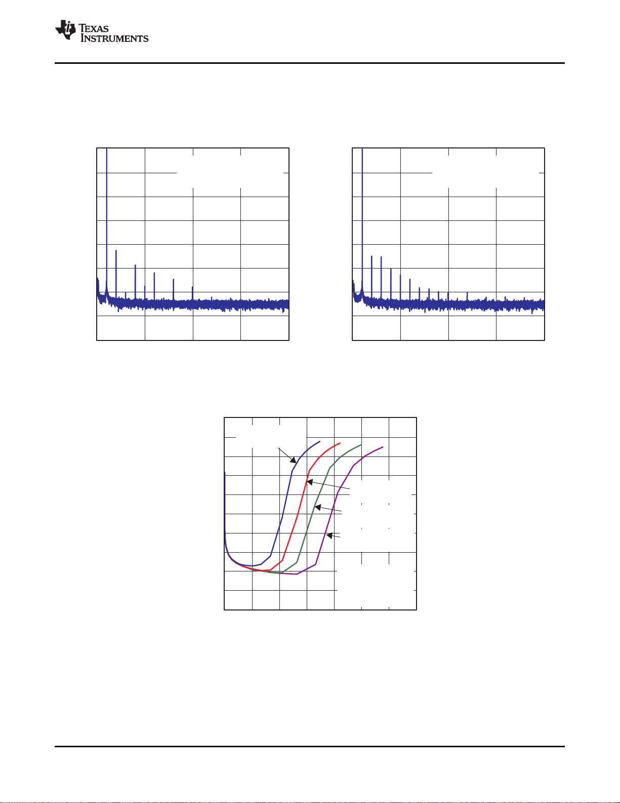
4 TYPICAL PERFORMANCE
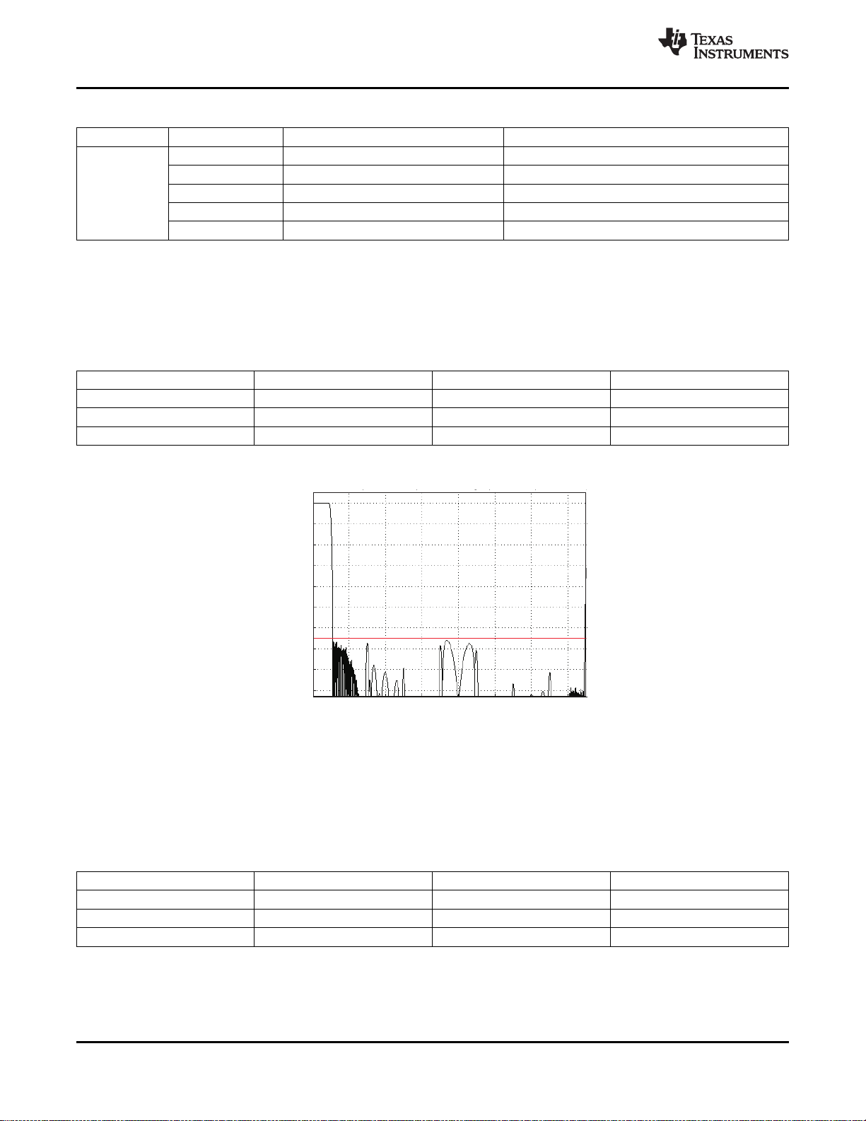
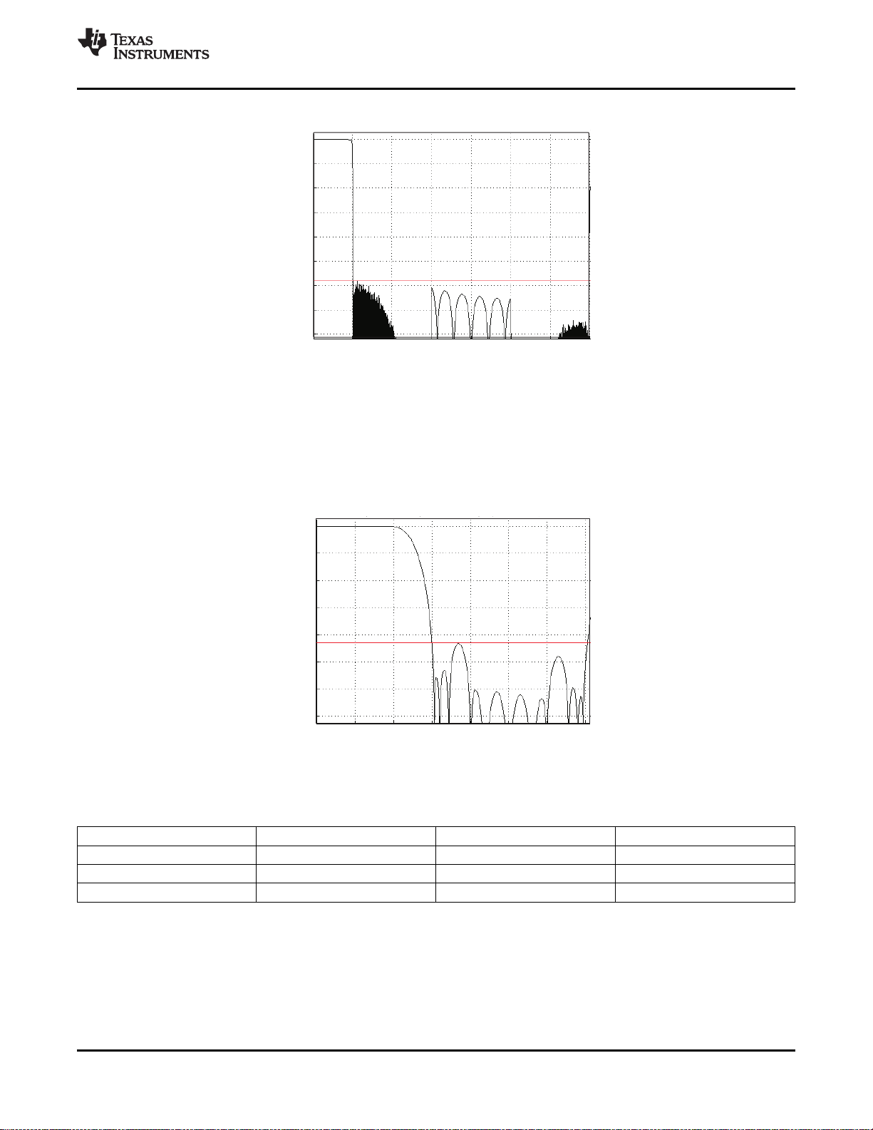
4.1 DAC Performance
AMPLITUDE AMPLITUDE
vs vs
FREQUENCY FREQUENCY
SLAS659–NOVEMBER 2009
Figure 4-1. FFT - DAC to Line Output Figure 4-2. FFT - DAC to Headphone Output
Copyright © 2009, Texas Instruments Incorporated TYPICAL PERFORMANCE 13
TOTAL HARMONIC DISTORTION + NOISE
vs
OUTPUT POWER
Figure 4-3. Headphone Output Power
Submit Documentation Feedback
Product Folder Link(s): TLV320DAC3120
Page 14
−70
−60
−50
−40
−30
−20
−10
0
0.0 0.5 1.0 1.5 2.0 2.5 3.0 3.5 4.0
G004
THD+N − Total Harmonic Distortion + Noise − dB
PO − Output Power − W
Driver Gain
= 6 dB
Driver Gain
= 12 dB
AVDD = HPVDD = 3.3 V
IOVDD = 3.3 V
SPKVDD = 5.5 V
DVDD = 1.8 V
RL = 4 Ω
Driver Gain
= 18 dB
Driver Gain
= 24 dB
−70
−60
−50
−40
−30
−20
−10
0
0.0 0.5 1.0 1.5 2.0 2.5 3.0 3.5 4.0
G005
THD+N − Total Harmonic Distortion + Noise − dB
PO − Output Power − W
AVDD = 3.3 V
HPVDD = 3.3 V
IOVDD = 3.3 V
DVDD = 1.8 V
Driver Gain = 18 dB
RL = 4 Ω
SPKVDD = 5.5 V
SPKVDD = 4.3 V
SPKVDD = 3.3 V
SPKVDD = 3.6 V
−70
−60
−50
−40
−30
−20
−10
0
0.0 0.5 1.0 1.5 2.0 2.5
G006
THD+N − Total Harmonic Distortion + Noise − dB
PO − Output Power − W
Driver Gain
= 6 dB
Driver Gain
= 12 dB
AVDD = HPVDD = 3.3 V
IOVDD = 3.3 V
SPKVDD = 5.5 V
DVDD = 1.8 V
RL = 8 Ω
Driver Gain
= 24 dB
Driver Gain
= 18 dB
−70
−60
−50
−40
−30
−20
−10
0
0.0 0.5 1.0 1.5 2.0 2.5 3.0
G007
THD+N − Total Harmonic Distortion + Noise − dB
PO − Output Power − W
AVDD = 3.3 V
HPVDD = 3.3 V
IOVDD = 3.3 V
DVDD = 1.8 V
Driver Gain = 18 dB
RL = 8 Ω
SPKVDD = 5.5 V
SPKVDD = 4.3 V
SPKVDD = 3.3 V
SPKVDD = 3.6 V
TLV320DAC3120
SLAS659–NOVEMBER 2009
4.2 Class-D Speaker Driver Performance
TOTAL HARMONIC DISTORTION + NOISE TOTAL HARMONIC DISTORTION + NOISE
vs vs
OUTPUT POWER OUTPUT POWER
Figure 4-4. Max Class-D Speaker-Driver Output Figure 4-5. Class-D Speaker-Driver Output Power
Power (RL= 4 Ω) (RL= 4 Ω)
TOTAL HARMONIC DISTORTION + NOISE TOTAL HARMONIC DISTORTION + NOISE
vs vs
OUTPUT POWER OUTPUT POWER
www.ti.com
Figure 4-6. Max Class-D Speaker-Driver Output Figure 4-7. Class-D Speaker-Driver Output Power
14 TYPICAL PERFORMANCE Copyright © 2009, Texas Instruments Incorporated
Power (RL= 8 Ω) (RL= 8 Ω)
Submit Documentation Feedback
Product Folder Link(s): TLV320DAC3120
Page 15
f − Frequency − kHz
−160
−140
−120
−100
−80
−60
−40
−20
0
0 5 10 15 20
Amplitude − dBFS
G008
AVDD = HPVDD = 3.3 V
IOVDD = SPKVDD = 3.3 V
DVDD = 1.8 V
f − Frequency − kHz
−160
−140
−120
−100
−80
−60
−40
−20
0
0 5 10 15 20
Amplitude − dBFS
G009
AVDD = HPVDD = 3.3 V
IOVDD = SPKVDD = 3.3 V
DVDD = 1.8 V
I − Current − mA
0.0
0.5
1.0
1.5
2.0
2.5
3.0
3.5
0.0 0.5 1.0 1.5 2.0 2.5 3.0 3.5 4.0
V − Voltage − V
G010
Micbias = 2 V
Micbias = 2.5 V
Micbias = AVDD (3.3 V)
TLV320DAC3120
www.ti.com
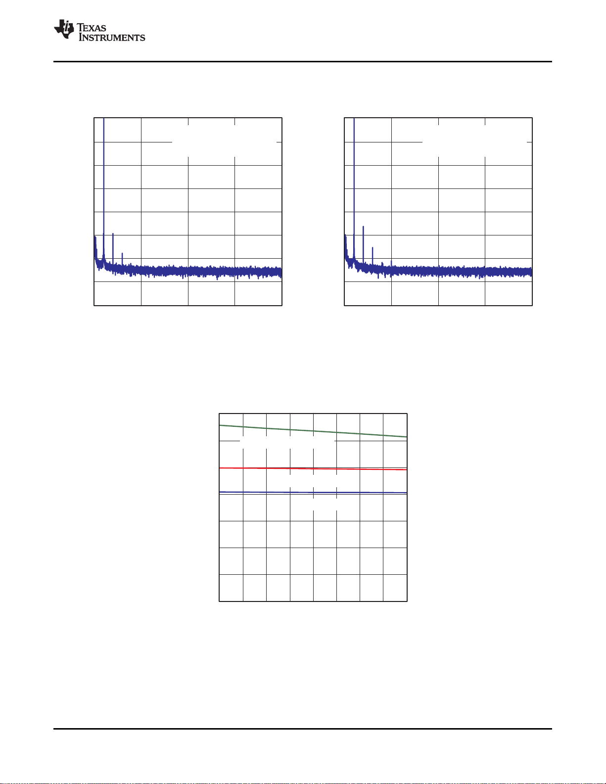
4.3 Analog Bypass Performance
AMPLITUDE AMPLITUDE
vs vs
FREQUENCY FREQUENCY
Figure 4-8. FFT - Line In Bypass to Line Output
SLAS659–NOVEMBER 2009
Figure 4-9. FFT - Line In Bypass to Headphone
Output
4.4 MICBIAS Performance
VOLTAGE
vs
CURRENT
Figure 4-10. Micbias
Copyright © 2009, Texas Instruments Incorporated TYPICAL PERFORMANCE 15
Submit Documentation Feedback
Product Folder Link(s): TLV320DAC3120
Page 16
HPVDD
HPVSSSPKVDD SPKVSS
AVDD
AVSSSPKVSS
VOL/MICDET
MICBIAS
TLV320DAC3120
SPKVDD
22 Fm0.1 Fm0.1 Fm 22 Fm
SVDD
AVDD
AVSS
0.1 Fm
10 Fm
0.1 Fm
10 Fm
+3.3VA
1 Fm
DVDD
DVSS IOVDD IOVSS
0.1 Fm 10 Fm
+1.8VD
IOVDD
0.1 Fm 10 Fm
Host Processor
SDIN
BCLK
WCLK
MCLK
SCL
SDA
RESET
GPIO1
S0400-06
AIN1
AIN2
To External
MIC Circuitry
Analog In
SPKM
SPKM
SPKP
SPKP
HPR
HPL
8- or
Speaker
W 4-W
Stereo
Headphone
Out
R1
34.8 kW
P1
25 kW
R2
9.76 kW
TLV320DAC3120
SLAS659–NOVEMBER 2009
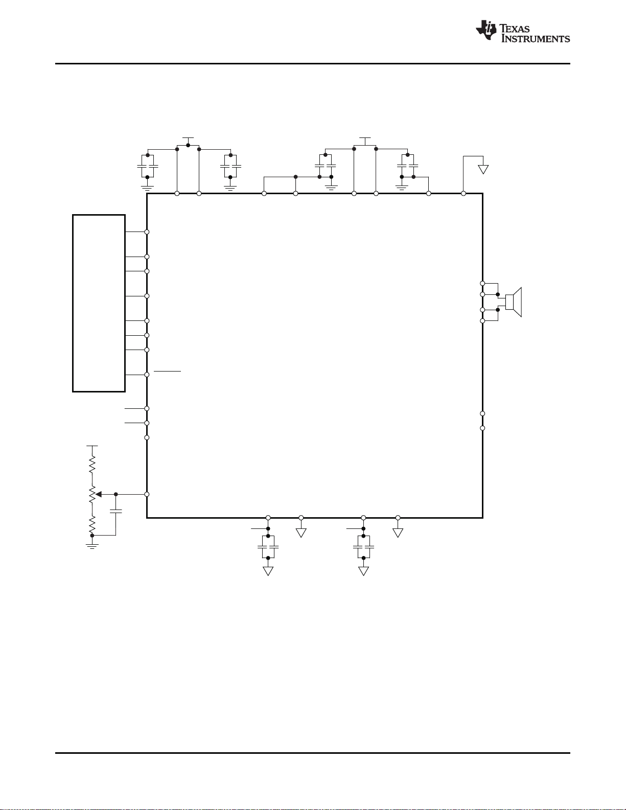
5 APPLICATION INFORMATION
5.1 Typical Circuit Configuration
www.ti.com
Figure 5-1. Typical Circuit Configuration
16 APPLICATION INFORMATION Copyright © 2009, Texas Instruments Incorporated
Submit Documentation Feedback
Product Folder Link(s): TLV320DAC3120
Page 17

TLV320DAC3120
www.ti.com
SLAS659–NOVEMBER 2009
5.2 Overview
The TLV320DAC3120 is a highly integrated mono audio DAC for portable computing, communication, and
entertainment applications. A register-based architecture eases integration with microprocessor-based
systems through standard serial-interface buses. This device contains a two-wire I2C bus interface, which
allows full register access. All peripheral functions are controlled through these registers and the onboard
state machines.
The TLV320DAC3120 consists of the following blocks:
• miniDSP digital signal-processing block
• Audio DAC
• Dynamic range compressor (DRC)
• Mono headphone/lineout amplifier
• Class-D mono amplifier capable of driving 4-Ω or 8-Ω speakers
• Pin-controlled or register-controlled volume level
• Power-down de-pop and power-up soft start
• Analog inputs
• I2C control interface
• Power-down control block
Following a toggle of the RESET pin or a software reset, the device operates in the default mode. The I2C
interface is used to write to the control registers to configure the device.
The I2C address assigned to the TLV320DAC3120 is 001 1000. This device always operates in an I2C
slave mode. All registers are 8-bit, and all writable registers have readback capability. The device
auto-increments to support sequential addressing and can be used with I2C fast mode. Once the device is
reset, all appropriate registers are updated by the host processor to configure the device as needed by the
user.
5.2.1 Device Initialization
5.2.1.1 Reset
The TLV320DAC3120 internal logic must be initialized to a known condition for proper device function. To
initialize the device to its default operating condition, the hardware reset pin (RESET) must be pulled low
for at least 10 ns. For this initialization to work, both the IOVDD and DVDD supplies must be powered up.
It is recommended that while the DVDD supply is being powered up, the RESET pin be pulled low.
The device can also be reset via software reset. Writing a 1 into page 0 / register 1, bit D0 resets the
device.
5.2.1.2 Device Start-Up Lockout Times
After the TLV320DAC3120 is initialized through hardware reset at power-up or software reset, the internal
memories are initialized to default values. This initialization takes place within 1 ms after pulling the
RESET signal high. During this initialization phase, no register-read or register-write operation should be
performed on the DAC coefficient buffers. Also, no block within the codec should be powered up during
the initialization phase.
5.2.1.3 PLL Start-Up
Whenever the PLL is powered up, a start-up delay of approximately of 10 ms occurs after the power-up
command of the PLL and before the clocks are available to the codec. This delay is to ensure stable
operation of the PLL and clock-divider logic.
Copyright © 2009, Texas Instruments Incorporated APPLICATION INFORMATION 17
Submit Documentation Feedback
Product Folder Link(s): TLV320DAC3120
Page 18

TLV320DAC3120
SLAS659–NOVEMBER 2009
5.2.1.4 Power-Stage Reset
The power-stage-only reset is used to reset the device after an overcurrent latching shutdown has
occurred. Using this reset re-enables the output stage without resetting all of the registers in the device.
Each of the two power stages has its own dedicated reset bit. The headphone power-stage reset is
performed by setting page 1 / register 31, bit D7 for HPOUT. The speaker power-stage reset is performed
by setting page 1 / register 32, bit D7 for SPKP and SPKM.
5.2.1.5 Software Power Down
By default, all circuit blocks are powered down following a reset condition. Hardware power up of each
circuit block can be controlled by writing to the appropriate control register. This approach allows the
lowest power-supply current for the functionality required. However, when a block is powered down, all of
the register settings are maintained as long as power is still being applied to the device.
5.2.2 Audio Analog I/O
The TLV320DAC3120 features a mono audio DAC. It supports a wide range of analog interfaces to
support different headsets and analog outputs. The TLV320DAC3120 interfaces to output drivers (8-Ω,
16-Ω, 32-Ω).
5.3 miniDSP
The TLV320DAC3120 features a miniDSP core which is tightly coupled to the DAC. The fully
programmable algorithms for the miniDSP must be loaded into the device after power up. The miniDSP
has direct access to the digital stereo audio stream, offering the possibility for advanced, very
low-group-delay DSP algorithms. The miniDSP has 1024 programmable instructions, 896 data memory
locations, and 512 programmable coefficients (in the adaptive mode, each bank has 256 programmable
coefficients).
www.ti.com
5.3.1 Software
Software development for the TLV320DAC3120 is supported through TI's comprehensive PurePath™
Studio software development environment, a powerful, easy-to-use tool designed specifically to simplify
software development on Texas Instruments miniDSP audio platforms. The graphical development
environment consists of a library of common audio functions that can be dragged and dropped into an
audio signal flow and graphically connected together. The DSP code can then be assembled from the
graphical signal flow with the click of a mouse. See the TLV320DAC3120 product folder on www.ti.com to
learn more about PurePath Studio and the latest status on available, ready-to-use DSP algorithms.
5.4 Digital Processing Low-Power Modes
The TLV320DAC3120 device can be tuned to minimize power dissipation, to maximize performance, or to
an operating point between the two extremes to best fit the application. The choice of processing blocks,
PRB_P4 to PRB_P22 for mono playback and PRB_R4 to PRB_R18 for mono recording, also influences
the power consumption. In fact, the numerous processing blocks have been implemented to offer a choice
among configurations having a different balance of power-optimization and signal-processing capabilities.
18 APPLICATION INFORMATION Copyright © 2009, Texas Instruments Incorporated
Submit Documentation Feedback
Product Folder Link(s): TLV320DAC3120
Page 19
TLV320DAC3120
www.ti.com
SLAS659–NOVEMBER 2009
5.4.1 DAC Playback on Headphones, Mono, 48 kHz, DVDD = 1.8 V, AVDD = 3.3 V, HPVDD = 3.3 V
DOSR = 128, Processing Block = PRB_P12 (Interpolation Filter B)
Power consumption = 15.4 mW
Table 5-1. PRB_P12 Alternative Processing Blocks, 15.4 mW
Processing Block Filter Estimated Power Change (mW)
PRB_P4 A 0.57
PRB_P5 A 1.48
PRB_P6 A 1.08
PRB_P13 B 0.56
PRB_P14 B 0.27
PRB_P15 B 0.89
PRB_P16 B 0.31
DOSR = 64, Processing Block = PRB_P12 (Interpolation Filter B)
Power consumption = 15.54 mW
Table 5-2. PRB_P12 Alternative Processing Blocks, 15.54 mW
Processing Block Filter Estimated Power Change (mW)
PRB_P4 A 0.37
PRB_P5 A 1.23
PRB_P6 A 1.15
PRB_P13 B 0.43
PRB_P14 B 0.13
PRB_P15 B 0.85
PRB_P16 B 0.21
5.4.2 DAC Playback on Headphones, Mono, 8 kHz, DVDD = 1.8 V, AVDD = 3.3 V, HPVDD = 3.3 V
DOSR = 768, Processing Block = PRB_P12 (Interpolation Filter B)
Power consumption = 14.49 mW
Table 5-3. PRB_P12 Alternative Processing Blocks, 14.49 mW
Processing Block Filter Estimated Power Change (mW)
PRB_P4 A –0.04
PRB_P5 A 0.2
PRB_P6 A –0.01
PRB_P13 B 0.1
PRB_P14 B 0.05
PRB_P15 B –0.03
PRB_P16 B 0.07
Copyright © 2009, Texas Instruments Incorporated APPLICATION INFORMATION 19
Submit Documentation Feedback
Product Folder Link(s): TLV320DAC3120
Page 20
TLV320DAC3120
SLAS659–NOVEMBER 2009
DOSR = 384, Processing Block = PRB_P12 (Interpolation Filter B)
Power consumption = 14.42 mW
Table 5-4. PRB_P12 Alternative Processing Blocks, 14.42 mW
Processing Block Filter Estimated Power Change (mW)
PRB_P4 A 0.16
PRB_P5 A 0.3
PRB_P6 A 0.2
PRB_P13 B 0.15
PRB_P14 B 0.07
PRB_P15 B 0.18
PRB_P16 B 0.09
5.5 Analog Signals
The TLV320DAC3120 analog signals consist of:
• Microphone bias (MICBIAS)
• Analog inputs AIN1 and AIN2, which can be used to pass-through or mix analog signals to output
stages
• Analog outputs class-D speaker driver and headphone/lineout driver providing output capability for the
DAC, AIN1, AIN2, or a mix of the three
www.ti.com
5.5.1 MICBIAS
The TLV320DAC3120 includes a microphone bias circuit which can source up to 4 mA of current, and is
programmable to a 2-V, 2.5-V, or AVDD level. The level can be controlled by writing to page 1 /
register 46, bits D1–D0. This functionality is shown in Table 5-5.
Table 5-5. MICBIAS Settings
D1 D0 FUNCTIONALITY
0 0 MICBIAS output is powered down.
0 1 MICBIAS output is powered to 2 V.
1 0 MICBIAS output is powered to 2.5 V.
1 1 MICBIAS output is powered to AVDD.
During normal operation, MICBIAS can be set to 2.5 V for better performance. However, depending on the
model of microphone that is selected, optimal performance might be obtained at another setting, so the
performance at a given setting should be verified.
The lowest current consumption occurs when MICBIAS is powered down. The next-lowest current
consumption occurs when MICBIAS is set at AVDD.
5.5.2 Analog Inputs AIN1 and AIN2
AIN1 (pin 13) and AIN2 (pin 14) are inputs to the output mixer along with the DAC output. Page 1 /
register 36 provides control signals for determining the signals routed through the output mixer. The output
of the output mixer then can be attenuated or amplified through the class-D and/or headphone/lineout
drivers.
20 APPLICATION INFORMATION Copyright © 2009, Texas Instruments Incorporated
Submit Documentation Feedback
Product Folder Link(s): TLV320DAC3120
Page 21

TLV320DAC3120
www.ti.com
SLAS659–NOVEMBER 2009
5.6 Audio DAC and Audio Analog Outputs
The mono audio DAC consists of a digital audio processing block, a digital interpolation filter, a digital
delta-sigma modulator, and an analog reconstruction filter. The high oversampling ratio (normally DOSR is
between 32 and 128) exhibits good dynamic range by ensuring that the quantization noise generated
within the delta-sigma modulator stays outside of the audio frequency band. Audio analog outputs include
mono headphone/lineout and mono class-D speaker outputs. Because the TLV320DAC3120 contains a
mono DAC, it inputs the mono data from the left channel, the right channel, or a mix of the left and right
channels as [(L + R) ÷ 2], selected by page 0 / register 63, bits D5–D4. See Figure 1-1 for the signal flow.
5.6.1 DAC
The TLV320DAC3120 mono audio DAC supports data rates from 8 kHz to 192 kHz. The audio channel of
the mono DAC consists of a signal-processing engine with fixed processing blocks, a programmable
miniDSP, a digital interpolation filter, multibit digital delta-sigma modulator, and an analog reconstruction
filter. The DAC is designed to provide enhanced performance at low sampling rates through increased
oversampling and image filtering, thereby keeping quantization noise generated within the delta-sigma
modulator and observed in the signal images strongly suppressed within the audio band to beyond 20
kHz. To handle multiple input rates and optimize power dissipation and performance, the
TLV320DAC3120 allows the system designer to program the oversampling rates over a wide range from 1
to 1024 by configuring page 0 / register 13 and page 0 / register 14. The system designer can choose
higher oversampling ratios for lower input data rates and lower oversampling ratios for higher input data
rates.
The TLV320DAC3120 DAC channel includes a built-in digital interpolation filter to generate oversampled
data for the delta-sigma modulator. The interpolation filter can be chosen from three different types,
depending on required frequency response, group delay, and sampling rate.
DAC power up is controlled by writing to page 0 / register 63, bit D7 for the mono channel. The
mono-channel DAC clipping flag is provided as a read-only bit on page 0 / register 39, bit D7.
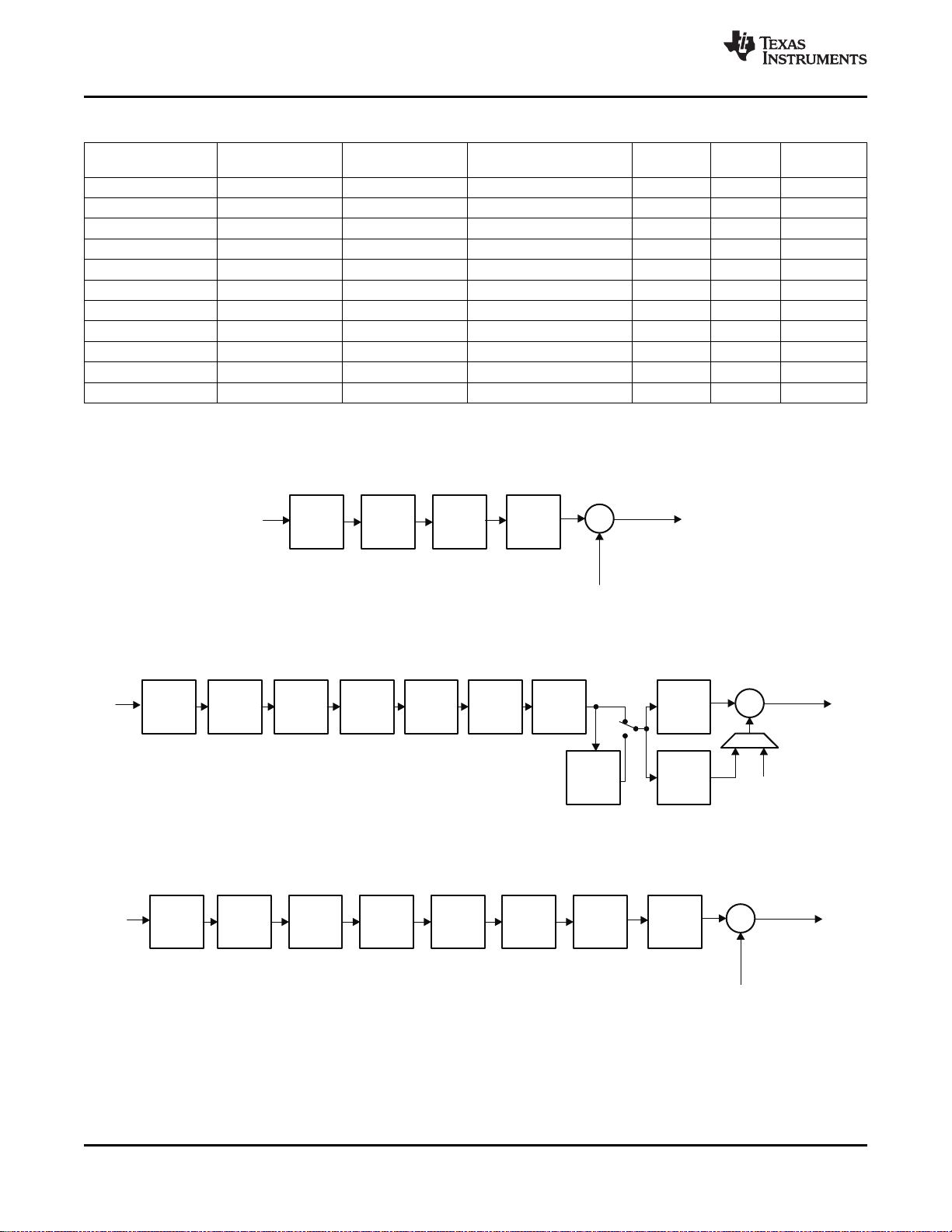
5.6.1.1 DAC Processing Blocks
The TLV320DAC3120 implements signal-processing capabilities and interpolation filtering via processing
blocks. These fixed processing blocks give users the choice of how much and what type of signal
processing they may use and which interpolation filter is applied.
The choices among these processing blocks allows the system designer to balance power conservation
and signal-processing flexibility. Table 5-6 gives an overview of all available processing blocks of the DAC
channel and their properties. The resource-class column gives an approximate indication of power
consumption for the digital (DVDD) supply; however, based on the out-of-band noise spectrum, the analog
power consumption of the drivers (HPVDD) may differ.
The signal-processing blocks available are:
• First-order IIR
• Scalable number of biquad filters
The processing blocks are tuned for common cases and can achieve high image rejection or low group
delay in combination with various signal-processing effects such as audio effects and frequency shaping.
The available first-order IIR and biquad filters have fully user-programmable coefficients.
Copyright © 2009, Texas Instruments Incorporated APPLICATION INFORMATION 21
Submit Documentation Feedback
Product Folder Link(s): TLV320DAC3120
Page 22
Interp.
Filter A
BiQuad
C
BiQuad
B
BiQuad
A
to
Modulator
Digital
Volume
Ctrl
from
Interface
´
Interp.
Filter
A,B
DRCHPF
BiQuad
F
BiQuad
E
BiQuad
D
BiQuad
C
BiQuad
B
BiQuad
A
IIR
to
Modulator
Digital
Volume
Ctrl
from
Interface
´
Interp.
Filter
A,B
BiQuad
F
BiQuad
E
BiQuad
D
BiQuad
C
BiQuad
B
BiQuad
A
IIR
to
Modulator
Digital
Volume
Ctrl
from
Interface
´
TLV320DAC3120
SLAS659–NOVEMBER 2009
Table 5-6. Overview – DAC Predefined Processing Blocks
Processing First-Order Number of Resource
Block No. IIR Available Biquads Class
PRB_P4 A Mono No 3 No 4
PRB_P5 A Mono Yes 6 Yes 6
PRB_P6 A Mono Yes 6 No 6
PRB_P12 B Mono Yes 0 No 3
PRB_P13 B Mono No 4 Yes 4
PRB_P14 B Mono No 4 No 4
PRB_P15 B Mono Yes 6 Yes 6
PRB_P16 B Mono Yes 6 No 4
PRB_P20 C Mono Yes 0 No 2
PRB_P21 C Mono Yes 4 Yes 3
PRB_P22 C Mono Yes 4 No 2
Interpolation Filter Channel DRC
5.6.1.2 DAC Processing Blocks – Signal Chain Details
5.6.1.2.1 Three Biquads, Filter A
www.ti.com
Figure 5-2. Signal Chain for PRB_P4
5.6.1.2.2 Six Biquads, First-Order IIR, DRC, Filter A or B
Figure 5-3. Signal Chain for PRB_P5 and PRB_P15
5.6.1.2.3 Six Biquads, First-Order IIR, Filter A or B
Figure 5-4. Signal Chain for PRB_P6 and PRB_P16
Submit Documentation Feedback
Product Folder Link(s): TLV320DAC3120
22 APPLICATION INFORMATION Copyright © 2009, Texas Instruments Incorporated
Page 23
Interp.
Filter
B,C
IIR
to
Modulator
Digital
Volume
Ctrl
from
Interface
´
Interp.
FilterB
DRCHPF
to
Modulator
Digital
Volume
Ctrl
BiQuad
D
BiQuad
C
BiQuad
B
BiQuad
A
from
Interface
´
Interp.
FilterB
BiQuad
D
BiQuad
C
BiQuad
B
BiQuad
A
to
Modulator
Digital
Volume
Ctrl
from
Interface
´
Interp.
FilterC
DRCHPF
IIR
to
Modulator
Digital
Volume
Ctrl
BiQuad
D
BiQuad
C
BiQuad
B
BiQuad
A
from
Interface
´
Interp.
FilterC
BiQuad
D
BiQuad
C
BiQuad
B
BiQuad
A
IIR
to
modulator
Digital
Volume
Ctrl
from
Interface
´
TLV320DAC3120
www.ti.com
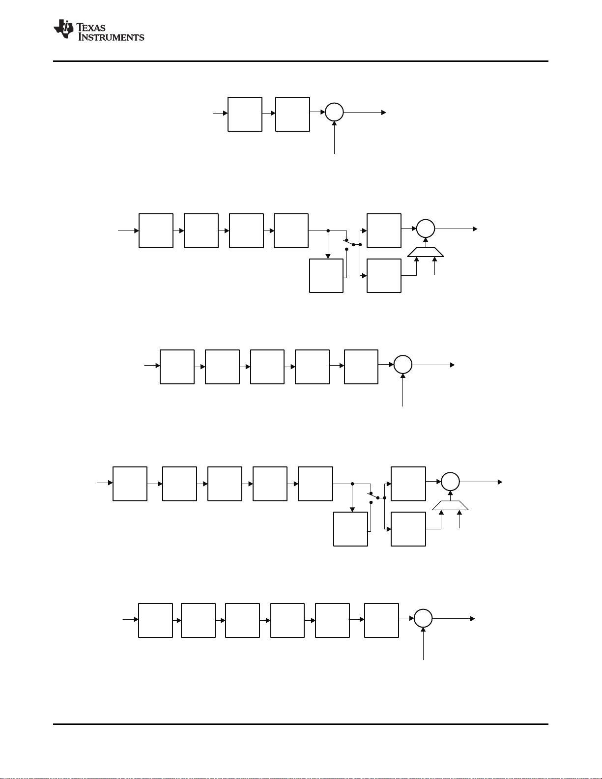
5.6.1.2.4 IIR, Filter B or C
Figure 5-5. Signal Chain for PRB_P12 and PRB_P20
5.6.1.2.5 Four Biquads, DRC, Filter B
Figure 5-6. Signal Chain for PRB_P13
5.6.1.2.6 Four Biquads, Filter B
SLAS659–NOVEMBER 2009
Figure 5-7. Signal Chain for PRB_P14
5.6.1.2.7 Four Biquads, First-Order IIR, DRC, Filter C
Figure 5-8. Signal Chain for PRB_P21
5.6.1.2.8 Four Biquads, First-Order IIR, Filter C
Figure 5-9. Signal Chain for PRB_P22
Product Folder Link(s): TLV320DAC3120
Submit Documentation Feedback
Copyright © 2009, Texas Instruments Incorporated APPLICATION INFORMATION 23
Page 24
LargestPositiveNumber:
=0.111 1111 1111 111
=0.999969482421875=1.0 – 1LSB
1
LargestNegativeNumber:
=1.0000 0000 0000 000
=0x8000= –1.0(bydefinition)
1 1 1
1 1 1
S.xxxx xxxx xxxx xxx.. x x x
SignBit
2 Bit
–1
2 Bit
–4
2 Bit
–15
Fraction
Point
TLV320DAC3120
SLAS659–NOVEMBER 2009
5.6.1.3 DAC User-Programmable Filters
Depending on the selected processing block, different types and orders of digital filtering are available. Up
to six biquad sections are available for specific processing blocks.
The coefficients of the available filters are arranged as sequentially-indexed coefficients in two banks. If
adaptive filtering is chosen, the coefficient banks can be switched in real time.
When the DAC is running, the user-programmable filter coefficients are locked and cannot be accessed
for either read or write.
However, the TLV320DAC3120 offers an adaptive filter mode as well. Setting page 8 / register 1,
bit D2 = 1 turns on double buffering of the coefficients. In this mode, filter coefficients can be updated
through the host and activated without stopping and restarting the DAC. This enables advanced adaptive
filtering applications.
In the double-buffering scheme, all coefficients are stored in two buffers (buffers A and B). When the DAC
is running and adaptive filtering mode is turned on, setting page 8 / register 1, bit D0 = 1 switches the
coefficient buffers at the next start of a sampling period. This bit is set back to 0 after the switch occurs. At
the same time, page 8 / register 1, bit D1 toggles.
The flag in page 8 / register 1, bit D1 indicates which of the two buffers is actually in use.
Page 8 / register 1, bit D1 = 0: buffer A is in use by the DAC engine; bit D1 = 1: buffer B is in use.
While the device is running, coefficient updates are always made to the buffer not in use by the DAC,
regardless of the buffer to which the coefficients have been written.
www.ti.com
Table 5-7. Adaptive-Mode Filter-Coefficient Buffer Switching
DAC Powered Up Page 8, Reg 1, Bit D1 I2C Writes to Updates
No 0 None Page 8, Reg 2–3, buffer A Page 8, Reg 2–3, buffer A
No 0 None Page 12, Reg 2–3, buffer Page 12, Reg 2–3, buffer B
Yes 0 Buffer A Page 8, Reg 2–3, buffer A Page 12, Reg 2–3, buffer B
Yes 0 Buffer A Page 12, Reg 2–3, buffer Page 12, Reg 2–3, buffer B
Yes 1 Buffer B Page 8, Reg 2–3, buffer A Page 8, Reg 2–3, buffer A
Yes 1 Buffer B Page 12, Reg 2–3, buffer Page 8, Reg 2–3, buffer A
Coefficient Buffer in
Use
B
B
B
The user-programmable coefficients for the DAC processing blocks are defined on pages 8 and 9 for
buffer A and pages 12 and 13 for buffer B.
The coefficients of these filters are each 16-bit, 2s-complement format, occupying two consecutive 8-bit
registers in the register space. Specifically, the filter coefficients are in 1.15 (one dot 15) format with a
range from –1.0 (0x8000) to 0.999969482421875 (0x7FFF) as shown in Figure 5-10.
24 APPLICATION INFORMATION Copyright © 2009, Texas Instruments Incorporated
Product Folder Link(s): TLV320DAC3120
Figure 5-10.
Submit Documentation Feedback
Page 25
1
0 1
15 1
1
N N z
H(z)
2 D z
-
-
+
=
-
1 2
0 1 2
15 1 2
1 2
N 2 N z N z
H(z)
2 2 D z D z
- -
- -
+ ´ +
=
- ´ -
TLV320DAC3120
www.ti.com
SLAS659–NOVEMBER 2009
5.6.1.3.1 First-Order IIR Section
The IIR is of first order and its transfer function is given by
The frequency response for the first-order IIR section with default coefficients is flat.
Table 5-8. DAC IIR Filter Coefficients
Filter Filter Coefficient Default (Reset) Values
First-order IIR N0 Page 9 / registers 2–3 0x7FFF (decimal 1.0 – LSB value)
N1 Page 9 / registers 4–5 0x0000
D1 Page 9 / registers 6–7 0x0000
DAC Coefficient,
Mono Channel
5.6.1.3.2 Biquad Section
The transfer function of each of the biquad filters is given by
Table 5-9. DAC Biquad Filter Coefficients
(1)
(2)
Filter Coefficient Mono DAC Channel Default (Reset) Values
Biquad A N0 Page 8 / registers 2–3 0x7FFF (decimal 1.0 – LSB value)
N1 Page 8 / registers 4–5 0x0000
N2 Page 8 / registers 6–7 0x0000
D1 Page 8 / registers 8–9 0x0000
D2 Page 8 / registers 10–11 0x0000
Biquad B N0 Page 8 / registers 12–13 0x7FFF (decimal 1.0 – LSB value)
N1 Page 8 / registers 14–15 0x0000
N2 Page 8 / registers 16–17 0x0000
D1 Page 8 / registers 18–19 0x0000
D2 Page 8 / registers 20–21 0x0000
Biquad C N0 Page 8 / registers 22–23 0x7FFF (decimal 1.0 – LSB value)
N1 Page 8 / registers 24–25 0x0000
N2 Page 8 / registers 26–27 0x0000
D1 Page 8 / registers 28–29 0x0000
D2 Page 8 / registers 30–31 0x0000
Biquad D N0 Page 8 / registers 32–33 0x7FFF (decimal 1.0 – LSB value)
N1 Page 8 / registers 34–35 0x0000
N2 Page 8 / registers 36–37 0x0000
D1 Page 8 / registers 38–39 0x0000
D2 Page 8 / registers 40–41 0x0000
Biquad E N0 Page 8 / registers 42–43 0x7FFF (decimal 1.0 – LSB value)
N1 Page 8 / registers 44–45 0x0000
N2 Page 8 / registers 46–47 0x0000
D1 Page 8 / registers 48–49 0x0000
D2 Page 8 / registers 50–51 0x0000
Copyright © 2009, Texas Instruments Incorporated APPLICATION INFORMATION 25
Submit Documentation Feedback
Product Folder Link(s): TLV320DAC3120
Page 26
0
–10
–20
–30
–40
–50
–60
–70
–80
–90
1
3 4
5 6
7
2
Magnitude – dB
FrequencyNormalizedtof
S
DACChannelResponseforInterpolationFilter A
(RedLineCorrespondsto –65dB)
TLV320DAC3120
SLAS659–NOVEMBER 2009
Table 5-9. DAC Biquad Filter Coefficients (continued)
Filter Coefficient Mono DAC Channel Default (Reset) Values
Biquad F N0 Page 8 / registers 52–53 0x7FFF (decimal 1.0 – LSB value)
N1 Page 8 / registers 54–55 0x0000
N2 Page 8 / registers 56–57 0x0000
D1 Page 8 / registers 58–59 0x0000
D2 Page 8 / registers 60–61 0x0000
5.6.1.4 DAC Interpolation Filter Characteristics
5.6.1.4.1 Interpolation Filter A
Filter A is designed for an fSup to 48 ksps with a flat pass band of 0 kHz–20 kHz.
Table 5-10. Specification for DAC Interpolation Filter A
Parameter Condition Value (Typical) Unit
Filter-gain pass band 0 … 0.45 f
Filter-gain stop band 0.55 fS… 7.455 f
Filter group delay 21/f
S
S
±0.015 dB
–65 dB
S
www.ti.com
s
5.6.1.4.2 Interpolation Filter B
Filter B is specifically designed for an fSup to 96 ksps. Thus, the flat pass-band region easily covers the
required audio band of 0 kHz–20 kHz.
Filter-gain pass band 0 … 0.45 f
Filter-gain stop band 0.55 fS… 3.45 f
Filter group delay 18/f
26 APPLICATION INFORMATION Copyright © 2009, Texas Instruments Incorporated
Parameter Condition Value (Typical) Unit
Figure 5-11. Frequency Response of DAC Interpolation Filter A
Table 5-11. Specification for DAC Interpolation Filter B
±0.015 dB
–58 dB
S
S
S
Submit Documentation Feedback
Product Folder Link(s): TLV320DAC3120
s
Page 27
DACChannelResponseforInterpolationFilterB
(RedLineCorrespondsto –58dB)
0.5 1 1.5 2 2.5 3 3.5
FrequencyNormalizedtof
S
0
–10
–20
–30
–40
–50
–60
–70
–80
Magnitude – dB
0
–10
–20
–30
–40
–50
–60
–70
Magnitude – dB
0 0.2 0.4 0.6 0.8 1 1.2 1.4
FrequencyNormalizedtof
S
DACChannelResponseforInterpolationFilterC
(RedLineCorrespondsto –43dB)
TLV320DAC3120
www.ti.com
SLAS659–NOVEMBER 2009
Figure 5-12. Frequency Response of Channel Interpolation Filter B
5.6.1.4.3 Interpolation Filter C
Filter C is specifically designed for the 192-ksps mode. The pass band extends up to 0.4 × f
(corresponds to 80 kHz), more than sufficient for audio applications.
S
Figure 5-13. Frequency Response of DAC Interpolation Filter C
Table 5-12. Specification for DAC Interpolation Filter C
Parameter Condition Value (Typical) Unit
Filter-gain pass band 0 … 0.35 f
Filter-gain stop band 0.6 fS… 1.4 f
Filter group delay 13/f
5.6.2 DAC Digital-Volume Control
The DAC has a digital volume-control block which implements programmable gain. Each channel has an
independent volume control that can be varied from 24 dB to –63.5 dB in 0.5-dB steps. The mono-channel
DAC volume can be controlled by writing to page 0 / register 65, bits D7–D0. DAC muting and setting up a
master gain control to control the mono channel is done by writing to page 0 / register 64, bits D3 and D1.
The gain is implemented with a soft-stepping algorithm, which only changes the actual volume by
Copyright © 2009, Texas Instruments Incorporated APPLICATION INFORMATION 27
S
S
Submit Documentation Feedback
Product Folder Link(s): TLV320DAC3120
±0.03 dB
–43 dB
S
s
Page 28

TLV320DAC3120
SLAS659–NOVEMBER 2009
0.125 dB per input sample, either up or down, until the desired volume is reached. The rate of
soft-stepping can be slowed to one step per two input samples by writing to page 0 / register 63, bits
D1–D0. Note that the default source for volume-control level settings is controlled by register writes to
page 0 / register 65. Use of the VOL/MICDET pin to control the DAC volume is ignored until the
volume-control source selected has been changed to pin control (page 0 / register 116, bit D7 = 1). This
functionality is shown in Figure 1-1.
During soft-stepping, the host does not receive a signal when the DAC has been completely muted. This
may be important if the host must mute the DAC before making a significant change, such as changing
sample rates. In order to help with this situation, the device provides a flag back to the host via a
read-only register, page 0 / register 38, bit D4 for the mono channel. This information alerts the host when
the part has completed the soft-stepping, and the actual volume has reached the desired volume level.
The soft-stepping feature can be disabled by writing to page 0 / register 63, bits D1–D0.
If soft-stepping is enabled, the CODEC_CLKIN signal should be kept active until the DAC power-up flag is
cleared. When this flag is cleared, the internal DAC soft-stepping process is complete, and
CODEC_CLKIN can be stopped if desired. (The analog volume control can be ramped down using an
internal oscillator.)
5.6.3 Volume-Control Pin
The range of voltages used by the 7-bit SAR ADC is shown in the Electrical Characteristics table.
The volume-control pin is not enabled by default, but it can be enabled by writing 1 to page 0 /
register 116, bit D7. The default DAC volume control uses software control of the volume, which occurs if
page 0 / register 116, bit D7 = 0. Soft-stepping the volume level is set up by writing to page 0 / register 63,
bits D1–D0.
www.ti.com
When the volume-pin function is used, a 7-bit Vol ADC reads the voltage on the VOL/MICDET pin and
updates the digital volume control. (It overwrites the current value of the volume control.) The new volume
setting which has been applied due to a change of voltage on the volume control pin can be read on
page 0 / register 117, bits D6–D0. The 7-bit Vol ADC clock source can be selected on page 0 /
register 116, bit D6. The update rate can be programmed on page 0 / register 116, bits D2–D0 for this
7-bit SAR ADC.
The VOL/MICDET pin gain mapping is shown in Table 5-13.
Table 5-13. VOL/MICDET Pin Gain Mapping
VOL/MICDET PIN SAR OUTPUT DIGITAL GAIN APPLIED
0 18 dB
1 17.5 dB
2 17 dB
: :
35 0.5 dB
36 0.0 dB
37 –0.5 dB
: :
89 –26.5 dB
90 –27 dB
91 –28 dB
: :
125 –62 dB
126 –63 dB
127 Mute
28 APPLICATION INFORMATION Copyright © 2009, Texas Instruments Incorporated
Submit Documentation Feedback
Product Folder Link(s): TLV320DAC3120
Page 29
1
0 1
HPF
15 1
1
N N z
H (z)
2 D z
-
-
+
=
-
1
0 1
LPF
15 1
1
N N z
H (z)
2 D z
-
-
+
=
-
TLV320DAC3120
www.ti.com
SLAS659–NOVEMBER 2009
The VOL/MICDET pin connection and functionality are shown in Figure 1-1.
As shown in Table 5-13, the VOL/MICDET pin has a range of volume control from 18 dB down to –63 dB,
and mute. However, if less maximum gain is required, then a smaller range of voltage should be applied
to the VOL/MICDET pin. This can be done by increasing the value of R2 relative to the value of (P1 + R1),
so that more voltage is available at the bottom of P1. The circuit should also be designed such that for the
values of R1, R2, and P1 chosen, the maximum voltage (top of the potentiometer) does not exceed
AVDD/2 (see Figure 5-1). The recommended values for R1, R2, and P1 for several maximum gains are
shown in Table 5-14. Note that In typical applications, R1 should not be 0 Ω, as the VOL/MICDET pin
should not exceed AVDD/2 for proper ADC operation.
Table 5-14. VOL/MICDET Pin Gain Scaling
R1 P1 R2 DIGITAL GAIN RANGE
(kΩ) (kΩ) (kΩ) (dB)
25 25 0 0 V to 1.65 V 18 dB to –63 dB
33 25 7.68 0.386 V to 1.642 V 3 dB to –63 dB
34.8 25 9.76 0.463 V to 1.649 V 0 dB to –63 dB
ADC VOLTAGE
for AVDD = 3.3 V
(V)
5.6.4 Dynamic Range Compression
Typical music signals are characterized by crest factors, the ratio of peak signal power to average signal
power, of 12 dB or more. To avoid audible distortions due to clipping of peak signals, the gain of the DAC
channel must be adjusted so as not to cause hard clipping of peak signals. As a result, during nominal
periods, the applied gain is low, causing the perception that the signal is not loud enough. To overcome
this problem, DRC in the TLV320DAC3120 continuously monitors the output of the DAC digital volume
control to detect its power level relative to 0 dBFS. When the power level is low, DRC increases the input
signal gain to make it sound louder. At the same time, if a peaking signal is detected, it autonomously
reduces the applied gain to avoid hard clipping. This results in sounds more pleasing to the ear as well as
sounding louder during nominal periods.
The DRC functionality in the TLV320DAC3120 is implemented by a combination of processing blocks in
the DAC channel as described in Section 5.6.1.2.
DRC can be disabled by writing to page 0 / register 68, bits D6–D5.
DRC typically works on the filtered version of the input signal. The input signals have no audio information
at dc and extremely low frequencies; however, they can significantly influence the energy estimation
function in DRC. Also, most of the information about signal energy is concentrated in the low-frequency
region of the input signal.
To estimate the energy of the input signal, the signal is first fed to the DRC high-pass filter and then to the
DRC low-pass filter. These filters are implemented as first-order IIR filters given by
(3)
(4)
The coefficients for these filters are 16 bits wide in 2s-complement format and are user-programmable
through register write as given in Table 5-15.
Copyright © 2009, Texas Instruments Incorporated APPLICATION INFORMATION 29
Submit Documentation Feedback
Product Folder Link(s): TLV320DAC3120
Page 30
TLV320DAC3120
SLAS659–NOVEMBER 2009
Table 5-15. DRC HPF and LPF Coefficients
Coefficient Location
HPF N0 C71 page 9 / registers 14 to 15
HPF N1 C72 page 9 / registers 16 to 17
HPF D1 C73 page 9 / registers 18 to 19
LPF N0 C74 page 9 / registers 20 to 21
LPF N1 C75 page 9 / registers 22 to 23
LPF D1 C76 page 9 / registers 24 to 25
The default values of these coefficients implement a high-pass filter with a cutoff at 0.00166 × DAC_fS,
and a low-pass filter with a cutoff at 0.00033 × DAC_fS.
The output of the DRC high-pass filter is fed to the processing block selected for the DAC channel. The
absolute value of the DRC-LPF filter is used for energy estimation within the DRC.
The gain in the DAC digital volume control is controlled by page 0 / registers 65 and 66. When the DRC is
enabled, the applied gain is a function of the digital volume-control register setting and the output of the
DRC.
The DRC parameters are described in sections that follow.
5.6.4.1 DRC Threshold
The DRC threshold represents the level of the DAC playback signal at which the gain compression
becomes active. The output of the digital volume control in the DAC is compared with the set threshold.
The threshold value is programmable by writing to page 0 / register 68, bits D4–D2. The threshold value
can be adjusted between –3 dBFS and –24 dBFS in steps of 3 dB. Keeping the DRC threshold value too
high may not leave enough time for the DRC block to detect peaking signals, and can cause excessive
distortion at the outputs. Keeping the DRC threshold value too low can limit the perceived loudness of the
output signal.
www.ti.com
The recommended DRC threshold value is –24 dB.
When the output signal exceeds the set DRC threshold, the interrupt flag bits at page 0 / register 44,
bits D3–D2 are updated. These flag bits are sticky in nature, and are reset only after they are read back
by the user. The non-sticky versions of the interrupt flags are also available at page 0 / register 46, bits
D3–D2.
5.6.4.2 DRC Hysteresis
DRC hysteresis is programmable by writing to page 0 / register 68, bits D1–D0. These bits can be
programmed to represent values between 0 dB and 3 dB in steps of 1 dB. It is a programmable window
around the programmed DRC threshold that must be exceeded for disabled DRC to become enabled, or
enabled DRC to become disabled. For example, if the DRC threshold is set to –12 dBFS and the DRC
hysteresis is set to 3 dB, then if the gain compression in DRC is inactive, the output of the DAC digital
volume control must exceed –9 dBFS before gain compression due to the DRC is activated. Similarly,
when the gain compression in the DRC is active, the output of the DAC digital volume control must fall
below –15 dBFS for gain compression in the DRC to be deactivated. The DRC hysteresis feature prevents
the rapid activation and de-activation of gain compression in DRC in cases when the output of the DAC
digital volume control rapidly fluctuates in a narrow region around the programmed DRC threshold. By
programming the DRC hysteresis as 0 dB, the hysteresis action is disabled.
The recommended value of DRC hysteresis is 3 dB.
30 APPLICATION INFORMATION Copyright © 2009, Texas Instruments Incorporated
Submit Documentation Feedback
Product Folder Link(s): TLV320DAC3120
Page 31

TLV320DAC3120
www.ti.com
SLAS659–NOVEMBER 2009
5.6.4.3 DRC Hold Time
DRC hold time is intended to slow the start of decay for a specified period of time in response to a
decrease in energy level. To minimize audible artifacts, it is recommended to set the DRC hold time to 0
through programming page 0 / register 69, bits D6–D3 = 0000.
5.6.4.4 DRC Attack Rate
When the output of the DAC digital volume control exceeds the programmed DRC threshold, the gain
applied in the DAC digital volume control is progressively reduced to prevent the signal from saturating the
channel. This process of reducing the applied gain is called attack. To avoid audible artifacts, the gain is
reduced slowly with a rate equaling the attack rate, programmable via page 0 / register 70, bits D7–D4.
Attack rates can be programmed from 4-dB gain change per sample period to 1.2207e–5-dB gain change
per sample period.
Attack rates should be programmed such that before the output of the DAC digital volume control can clip,
the input signal should be sufficiently attenuated. High attack rates can cause audible artifacts, and
too-slow attack rates may not be able to prevent the input signal from clipping.
The recommended DRC attack rate value is 1.9531e–4 dB per sample period.
5.6.4.5 DRC Decay Rate
When the DRC detects a reduction in output signal swing beyond the programmed DRC threshold, the
DRC enters a decay state, where the applied gain in the digital-volume control is gradually increased to
programmed values. To avoid audible artifacts, the gain is slowly increased with a rate equal to the decay
rate programmed through page 0 / register 70, bits D3–D0. The decay rates can be programmed from
1.5625e–3 dB per sample period to 4.7683e–7 dB per sample period. If the decay rates are programmed
too high, then sudden gain changes can cause audible artifacts. However, if it is programmed too slow,
then the output may be perceived as too low for a long time after the peak signal has passed.
The recommended Value of DRC attack rate is 2.4414e–5 dB per sample period.
5.6.4.6 Example Setup for DRC
• DAC vol gain = 12 dB
• Threshold = –24 dB
• Hysteresis = 3 dB
• Hold time = 0 ms
• Attack rate = 1.9531e–4 dB per sample period
• Decay rate = 2.4414e–5 dB per sample period
Script
#Go to Page 0 w 30 00 00 #DAC => 12 db gain mono w 30 41 18 #DAC => DRC Enabled, Threshold = 24 db, Hysteresis = 3 dB w 30 44 7F #DRC Hold = 0 ms, Rate of Changes of Gain = 0.5 dB/Fs' w 30
45 00 #Attack Rate = 1.9531e-4 dB/Frame , DRC Decay Rate =2.4414e-5 dB/Frame w 30 46 B6 #Go to
Page 9 w 30 00 09 #DRC HPF w 30 0E 7F AB 80 55 7F 56 #DRC LPF W 30 14 00 11 00 11 7F DE
5.6.4.7 Headset Detection
The TLV320DAC3120 includes extensive capability to monitor a headphone, microphone, or headset jack,
to determine if a plug has been inserted into the jack, and then determine what type of
headset/headphone is wired to the plug. The device also includes the capability to detect a button press,
even, for example, when starting calls on mobile phones with headsets. Figure 5-14 shows the circuit
configuration to enable this feature.
Copyright © 2009, Texas Instruments Incorporated APPLICATION INFORMATION 31
Submit Documentation Feedback
Product Folder Link(s): TLV320DAC3120
Page 32

g
s
m
Micbias
m
s
g
MICBIAS
HPOUT
VOL/MICDET
Micpga
Hpout
S0403-01
TLV320DAC3120
SLAS659–NOVEMBER 2009
Figure 5-14. Jack Connections for Headset Detection
This feature is enabled by programming page 0 / register 67, bit D1. In order to avoid false detections due
to mechanical vibrations in headset jacks or microphone buttons, a debounce function is provided for
glitch rejection. For the case of headset insertion, a debounce function with a range of 32 ms to 512 ms is
provided. This can be programmed via page 0 / register 67, bits D4–D2. For improved button-press
detection, the debounce function has a range of 8 ms to 32 ms by programming page 0 / register 67,
bits D1–D0.
www.ti.com
The TLV320DAC3120 also provides feedback to the user when a button press or a headset
insertion/removal event is detected through register-readable flags or an interrupt on the I/O pins. The
value in page 0 / register 46, bits D5–D4 provides the instantaneous state of button press and headset
insertion. Page 0 / register 44, bit D5 is a sticky (latched) flag that is set when the button-press event is
detected. Page 0 / register 44, bit D4 is a sticky flag which is set when the headset insertion or removal
event is detected. These sticky flags are set by the event occurrence, and are reset only when read. This
requires polling page 0 / register 44. To avoid polling and the associated overhead, the TLV320DAC3120
also provides an interrupt feature whereby the events can trigger the INT1 and/or INT2 interrupts. These
interrupt events can be routed to one of the digital output pins. See Section 5.6.4.8 for details.
The TLV320DAC3120 not only detects a headset-insertion event, but also is able to distinguish between
the different headsets inserted, such as stereo headphones or cellular headphones. After the
headset-detection event, the user can read page 0 / register 67, bits D6–D5 to determine the type of
headset inserted.
Table 5-16. Headset-Detection Block Registers
Register Description
Page 0 / register 67, bit D1 Headset-detection enable/disable
Page 0 / register 67, bits D4–D2 Debounce programmability for headset detection
Page 0 / register 67, bits D1–D0 Debounce programmability for button press
Page 0 / register 44, bit D5 Sticky flag for button-press event
Page 0 / register 44, bit D4 Sticky flag for headset-insertion or -removal event
Page 0/ register 46, bit D5 Status flag for button-press event
Page 0 / register 46, bit D4 Status flag for headset insertion and removal
Page 0 / register 67, bits D6–D5 Flags for type of headset detected
32 APPLICATION INFORMATION Copyright © 2009, Texas Instruments Incorporated
Submit Documentation Feedback
Product Folder Link(s): TLV320DAC3120
Page 33

TLV320DAC3120
www.ti.com
SLAS659–NOVEMBER 2009
The headset detection block requires AVDD to be powered. The headset-detection feature in the
TLV320DAC3120 is achieved with very low power overhead, requiring less than 20 μA of additional
current from the AVDD supply.
5.6.4.8 Interrupts
Some specific events in the TLV320DAC3120, which may require host-processor intervention, can be
used to trigger interrupts to the host processor. This avoids polling the status-flag registers continuously.
The TLV320DAC3120 has two defined interrupts, INT1 and INT2, that can be configured by programming
page 0 / register 48 and page 0 / register 49. A user can configure interrupts INT1 and INT2 to be
triggered by one or many events, such as:
• Headset detection
• Button press
• DAC DRC signal exceeding threshold
• Noise detected by AGC
• Overcurrent condition in headphone drivers/speaker drivers
• Data overflow in the DAC processing blocks and filters
• DC measurement data available
Each of these INT1 and INT2 interrupts can be routed to output pin GPIO1. These interrupt signals can
either be configured as a single pulse or a series of pulses by programming page 0 / register 48, bit D0
and page 0 / register 49, bit D0. If the user configures the interrupts as a series of pulses, the events
trigger the start of pulses that stop when the flag registers in page 0 / register 44, page 0 / register 45, and
page 0 / register 50 are read by the user to determine the cause of the interrupt.
5.6.5 Programming DAC Digital Filter Coefficients
The digital filter coefficients must be programmed through the I2C interface. All digital filtering for the DAC
signal path must be loaded into the RAM before the DAC is powered on. (Note that default ALLPASS filter
coefficients for programmable biquads are located in boot ROM. The boot ROM automatically loads the
default values into the RAM following a hardware reset (toggling the RESET pin) or after a software reset.
After resetting the device, loading boot ROM coefficients into the digital filters requires 100 μs of
programming time. During this time, reading or writing to page 8 through page 15 for updating DAC filter
coefficient values is not permitted. (The DAC should not be powered up until after all of the DAC
configurations have been done by the system microprocessor.)
5.6.6 Updating DAC Digital Filter Coefficients During PLAY
When it is required to update the DAC digital filter coefficients during play, care must be taken to avoid
click and pop noise or even a possible oscillation noise. These artifacts can occur if the DAC coefficients
are updated without following the proper update sequence. The correct sequence is shown in Figure 5-15.
The values for times listed in Figure 5-15 are conservative and should be used for software purposes.
There is also an adaptive mode, in which DAC coefficients can be updated while the DAC is on. For
details, see Section 5.6.1.3.
Copyright © 2009, Texas Instruments Incorporated APPLICATION INFORMATION 33
Submit Documentation Feedback
Product Folder Link(s): TLV320DAC3120
Page 34

Play- Paused
DACPowerDown
Update
DigitalFilter
Coefficients
DACPowerUP
Wait20ms
VolumeRampDown
SoftMute
Restore Previous
VolumeLevel(Ramp)
in(B)ms
Play- Continue
Wait(A)ms
Forf =32kHzS® Wait25ms(min)
Forf =48kHz Wait20ms(min)
S
®
For =32kHz ®f 25ms
Forf =48kHz 20ms
S
S
®
DACVolumeRampDownWAIT Time(A)
DACVolumeRampUp Time(B)
F0024-02
TLV320DAC3120
SLAS659–NOVEMBER 2009
www.ti.com
Figure 5-15. Example Flow For Updating DAC Digital Filter Coefficients During Play
5.6.7 Digital Mixing and Routing
The TLV320DAC3120 has four digital mixing blocks. Each mixer can provide either mixing or multiplexing
of the digital audio data. The first mixer/multiplexer can be used to select input data for the mono DAC
from left channel, right channel, or a mix of the left and right channels [(L + R) / 2]. This digital routing can
be configured by writing to page 0 / register 63, bits D5–D4 for the DAC mono channel.
5.6.8 Analog Audio Routing
The TLV320DAC3120 has the capability to route the DAC output to either the headphone or the speaker
output. If desirable, both output drivers can be operated at the same time while playing at different volume
levels. The TLV320DAC3120 provides various digital routing capabilities, allowing digital mixing or even
channel swapping in the digital domain. All analog outputs other than the selected ones can be powered
down for optimal power consumption.
34 APPLICATION INFORMATION Copyright © 2009, Texas Instruments Incorporated
Submit Documentation Feedback
Product Folder Link(s): TLV320DAC3120
Page 35

TLV320DAC3120
www.ti.com
SLAS659–NOVEMBER 2009
5.6.8.1 Analog Output Volume Control
The output volume control can be used to fine-tune the level of the mixer amplifier signal supplied to the
headphone driver or the speaker driver. This architecture supports separate and concurrent volume levels
for each of the four output drivers. This volume control can also be used as part of the output pop-noise
reduction scheme. This feature is available even if the DAC is powered down.
5.6.8.2 Headphone Analog Output Volume Control
For the headphone outputs, the analog volume control has a range from 0 dB to –78 dB in 0.5-dB steps
for most of the useful range plus mute, as shown in Table 5-17 and Table 5-18. This volume control
includes soft-stepping logic. Routing the DAC output signal to the analog volume control is done by writing
to page 1 / register 35, bits D7–D6.
Changing the analog volume for the headphone is controlled by writing to page 1 / register 36,
bits D6–D0. Routing the signal from the output of the analog volume control to the input of the headphone
power amplifier is done by writing to page 1 / register 36, bit D7.
The analog volume-control soft-stepping time is based on the setting in page 0 / register 63, bits D1–D0.
Copyright © 2009, Texas Instruments Incorporated APPLICATION INFORMATION 35
Submit Documentation Feedback
Product Folder Link(s): TLV320DAC3120
Page 36

TLV320DAC3120
SLAS659–NOVEMBER 2009
www.ti.com
Table 5-17. Analog Volume Control for Headphone and Speaker Outputs (for D7 = 0)
Register Value Attenuation Register Value Attenuation Register Value Attenuation Register Value Attenuation
0 0.0 30 –15.1 60 –30.1 90 –45.4
1 –0.5 31 –15.6 61 –30.7 91 –46.0
2 –1.0 32 –16.0 62 –31.1 92 –46.4
3 –1.5 33 –16.5 63 –31.7 93 –46.9
4 –2.0 34 –17.1 64 –32.2 94 –47.6
5 –2.5 35 –17.6 65 –32.7 95 –48.2
6 –3.0 36 –18.1 66 –33.2 96 –48.4
7 –3.5 37 –18.6 67 –33.7 97 –49.0
8 –4.0 38 –19.1 68 –34.2 98 –49.6
9 –4.5 39 –19.6 69 –34.7 99 –50.3
10 –5.0 40 –20.1 70 –35.2 100 –50.7
11 –5.5 41 –20.6 71 –35.7 101 –51.4
12 –6.0 42 –21.1 72 –36.2 102 –51.8
13 –6.5 43 –21.6 73 –36.8 103 –52.2
14 –7.0 44 –22.1 74 –37.2 104 –52.7
15 –7.5 45 –22.6 75 –37.8 105 –53.2
16 –8.0 46 –23.1 76 –38.3 106 –54.2
17 –8.5 47 –23.6 77 –38.8 107 –54.7
18 –9.0 48 –24.1 78 –39.3 108 –56.0
19 –9.5 49 –24.6 79 –39.8 109 –57.4
20 –10.0 50 –25.1 80 –40.3 110 –59.2
21 –10.5 51 –25.6 81 –40.8 111 –61.4
22 –11.0 52 –26.1 82 –41.4 112 –64.3
23 –11.5 53 –26.6 83 –41.9 113 –66.2
24 –12.0 54 –27.1 84 –42.3 114 –68.7
25 –12.5 55 –27.6 85 –42.9 115 –72.2
26 –13.0 56 –28.1 86 –43.3 116 –78.3
27 –13.5 57 –28.6 87 –43.9 117–127 PGA is muted.
28 –14.1 58 –29.1 88 –44.5
29 –14.6 59 –29.6 89 –45.0
Analog Analog Analog Analog
(dB) (dB) (dB) (dB)
36 APPLICATION INFORMATION Copyright © 2009, Texas Instruments Incorporated
Submit Documentation Feedback
Product Folder Link(s): TLV320DAC3120
Page 37

TLV320DAC3120
www.ti.com
SLAS659–NOVEMBER 2009
Table 5-18. Analog Volume Control for Headphone and Speaker Outputs (for D7 = 1)
Register Value Attenuation Register Value Attenuation Register Value Attenuation Register Value Attenuation
0 0.0 30 –15.0 60 –30.1 90 –45.2
1 –0.5 31 –15.5 61 –30.6 91 –45.8
2 –1.0 32 –16.0 62 –31.1 92 –46.2
3 –1.5 33 –16.5 63 –31.6 93 –46.7
4 –2.0 34 –17.0 64 –32.1 94 –47.4
5 –2.5 35 –17.5 65 –32.6 95 –47.9
6 –3.0 36 –18.1 66 –33.1 96 –48.2
7 –3.5 37 –18.6 67 –33.6 97 –48.7
8 –4.0 38 –19.1 68 –34.1 98 –49.3
9 –4.5 39 –19.6 69 –34.6 99 –50.0
10 –5.0 40 –20.1 70 –35.2 100 –50.3
11 –5.5 41 –20.6 71 –35.7 101 –51.0
12 –6.0 42 –21.1 72 –36.2 102 –51.4
13 –6.5 43 –21.6 73 –36.7 103 –51.8
14 –7.0 44 –22.1 74 –37.2 104 –52.2
15 –7.5 45 –22.6 75 –37.7 105 –52.7
16 –8.0 46 –23.1 76 –38.2 106 –53.7
17 –8.5 47 –23.6 77 –38.7 107 –54.2
18 –9.0 48 –24.1 78 –39.2 108 –55.3
19 –9.5 49 –24.6 79 –39.7 109 –56.7
20 –10.0 50 –25.1 80 –40.2 110 –58.3
21 –10.5 51 –25.6 81 –40.7 111 –60.2
22 –11.0 52 –26.1 82 –41.2 112 –62.7
23 –11.5 53 –26.6 83 –41.7 113 –64.3
24 –12.0 54 –27.1 84 –42.1 114 –66.2
25 –12.5 55 –27.6 85 –42.7 115 –68.7
26 –13.0 56 –28.1 86 –43.2 116 –72.2
27 –13.5 57 –28.6 87 –43.8 117–127 –78.3
28 –14.0 58 –29.1 88 –44.3
29 –14.5 59 –29.6 89 –44.8
Analog Analog Analog Analog
(dB) (dB) (dB) (dB)
5.6.8.3 Class-D Speaker Analog Output Volume Control
For the speaker outputs, the analog volume control has a range from 0 dB to –78 dB in 0.5-dB steps for
most of the useful range plus mute, as seen in Table 5-17 and Table 5-18. The implementation includes
soft-stepping logic.
Routing the DAC output signal to the analog volume control is done by writing to page 1 / register 35,
bits D7–D6. Changing the analog volume for the speaker is controlled by writing to page 1 / register 38,
bits D6–D0.
Routing the signal from the output of the analog volume control to the input of the speaker amplifier is
done by writing to page 1 / register 38, bit D7.
The analog volume-control soft-stepping time is based on the setting in page 0 / register 63, bits D1–D0.
5.6.9 Analog Outputs
Various analog routings are supported for playback. All the options can be conveniently viewed on the
functional block diagram, Figure 1-1.
Copyright © 2009, Texas Instruments Incorporated APPLICATION INFORMATION 37
Submit Documentation Feedback
Product Folder Link(s): TLV320DAC3120
Page 38

TLV320DAC3120
SLAS659–NOVEMBER 2009
5.6.9.1 Headphone Drivers
The TLV320DAC3120 features a mono headphone driver (HPOUT) that can deliver up to 30 mW per
channel, at 3.3-V supply voltage, into a 16-Ω load. The headphones are used in a single-ended
configuration where an ac-coupling (dc-blocking) capacitor is connected between the device output pins
and the headphones. The headphone driver also supports 32-Ω and 10-kΩ loads without changing any
control register settings.
The headphone drivers can be configured to optimize the power consumption in the lineout-drive mode by
writing 11 to page 0 / register 44, bits D2–D1.
The output common mode of the headphone/lineout drivers can be programmed to 1.35 V, 1.5 V, 1.65 V,
or 1.8 V by setting page 1 / register 31, bits D4–D3. The common-mode voltage should be set ≤ AVDD/2.
The headphone driver can be powered on by writing to page 1 / register 31, bit D7. The HPOUT output
driver gain can be controlled by writing to page 1 / register 40, bits D6–D3, and it can be muted by writing
to page 1 / register 40, bit D2.
The TLV320DAC3120 has a short-circuit protection feature for the headphone drivers, which is always
enabled to provide protection. The output condition of the headphone driver during short circuit can be
programmed by writing to page 1 / register 31, bit D1. If D1 = 0 when a short circuit is detected, the device
limits the maximum current to the load. If D1 = 1 when a short circuit is detected, the device powers down
the output driver. The default condition for headphones is the current-limiting mode. In case of a short
circuit on either channel, the output is disabled and a status flag is provided as read-only bits on page 1 /
register 31, bit D0. If shutdown mode is enabled, then as soon as the short circuit is detected, page 1 /
register 31, bit D7 (for HPLOUT) clears automatically. Next, the device requires a reset to re-enable the
output stage. Resetting can be done in two ways. First, the device master reset can be used, which
requires either toggling the RESET pin or using the software reset. If master reset is used, it resets all of
the registers. Second, a dedicated headphone power-stage reset can also be used to re-enable the output
stage, and that keeps all of the other device settings. The headphone power stage reset is done by setting
page 1 / register 31, bit D7 for HPLOUT. If the fault condition has been removed, then the device returns
to normal operation. If the fault is still present, then another shutdown occurs. Repeated resetting (more
than three times) is not recommended, as this could lead to overheating.
www.ti.com
5.6.9.2 Speaker Drivers
The TLV320DAC3120 has an integrated class-D mono speaker driver (SPKP/SPKM) capable of driving an
8-Ω or 4-Ω differential load. The speaker driver can be powered directly from the battery supply (2.7 V to
5.5 V) on the SPKVDD pins; however, the voltage (including spike voltage) must be limited below the
absolute-maximum voltage of 6 V.
The speaker driver is capable of supplying 400 mW per channel with a 3.6-V power supply. Through the
use of digital mixing, the device can connect one or both digital audio playback data channels to either
speaker driver; this also allows digital channel swapping if needed.
The class-D speaker driver can be powered on by writing to page 1 / register 32, bit D7. The class-D
output-driver gain can be controlled by writing to page 1 / register 42, bits D4–D3, and it can be muted by
writing to page 1 / register 42, bit D2.
The TLV320DAC3120 has a short-circuit protection feature for the speaker drivers that is always enabled
to provide protection. If the output is shorted, the output stage shuts down on the overcurrent condition.
(Current limiting is not an available option for the higher-current speaker driver output stage.) In case of a
short circuit, the output is disabled and a status flag is provided as a read-only bit on page 1 / register 32,
bit D0.
38 APPLICATION INFORMATION Copyright © 2009, Texas Instruments Incorporated
Submit Documentation Feedback
Product Folder Link(s): TLV320DAC3120
Page 39

TLV320DAC3120
www.ti.com
SLAS659–NOVEMBER 2009
If shutdown occurs due to an overcurrent condition, then the device requires a reset to re-enable the
output stage. Resetting can be done in two ways. First, the device master reset can be used, which
requires either toggling the RESET pin or using the software reset. If master reset is used, it resets all of
the registers. Second, a dedicated speaker power-stage reset can be used that keeps all of the other
device settings. The speaker power-stage reset is done by setting page 1 / register 32, bit D7 for SPKP
and SPKM. If the fault condition has been removed, then the device returns to normal operation. If the
fault is still present, then another shutdown occurs. Repeated resetting (more than three times) is not
recommended, as this could lead to overheating.
To minimize battery current leakage, the SPKVDD voltage level should not be less than the AVDD
voltage level.
The TLV320DAC3120 has a thermal protection (OTP) feature for the speaker drivers which is always
enabled to provide protection. If the device is overheated, then the output stops switching. When the
device cools down, the output resumes switching. An overtemperature status flag is provided as a
read-only bit on page 0 / register 3, bit D1. The OTP feature is for self-protection of the device. If die
temperature can be controlled at the system/board level, then overtemperature does not occur.
5.6.10 Audio Output-Stage Power Configurations
After the device has been configured (following a RESET) and the circuitry has been powered up, the
audio output stage can be powered up and powered down by register control.
These functions soft-start automatically. By using these register controls, it is possible to turn all four
stages on at the same time without turning two of them off.
See Table 5-19 for register control of audio output stage power configurations.
Table 5-19. Audio Output Stage Power Configurations
Audio Output Pins Desired Function Page 1 / Register, Bit Value
HPOUT Power-down HPOUT driver Page 1 / register 31, bit D7 = 0
HPOUT Power-up HPOUT driver Page 1 / register 31, bit D7 = 1
SPKP / SPKM Power-down class-D driver Page 1 / register 32, bit D7 = 0
SPKP / SPKM Power-up class-D driver Page 1 / register 32, bit D7 = 1
5.7 CLOCK Generation and PLL
The TLV320DAC3120 supports a wide range of options for generating clocks for the DAC sections as well
as interface and other control blocks as shown in Figure 5-16. The clocks for the DAC require a source
reference clock. This clock can be provided on a variety of device pins, such as the MCLK, BCLK, or
GPIO1 pins. The source reference clock for the codec can be chosen by programming the
CODEC_CLKIN value on page 0 / register 4, bits D1–D0. The CODEC_CLKIN can then be routed through
highly-flexible clock dividers shown in Figure 5-16 to generate the various clocks required for the DAC and
the miniDSP section. In the event that the desired audio clocks cannot be generated from the reference
clocks on MCLK, BCLK, or GPIO1, the TLV320DAC3120 also provides the option of using the on-chip
PLL which supports a wide range of fractional multiplication values to generate the required clocks.
Starting from CODEC_CLKIN, the TLV320DAC3120 provides several programmable clock dividers to help
achieve a variety of sampling rates for the DAC and clocks for the miniDSP sections.
Copyright © 2009, Texas Instruments Incorporated APPLICATION INFORMATION 39
Submit Documentation Feedback
Product Folder Link(s): TLV320DAC3120
Page 40

PLL
´ ´(R J.D)/P
PLL_CLKIN
CODEC_CLKIN
DAC_MOD_CLK
DAC_CLK
NDAC = 1, 2, ..., 127, 128
MDAC = 1, 2, ..., 127, 128
DOSR = 1, 2, ..., 1023, 1024
MCLK
BCLK
GPIO1
DIN
MCLK
BCLK
GPIO1
PLL_CLK
¸ MDAC
¸ DOSR
¸ NDAC
To DAC miniDSP
Clock Generation
DAC_f
S
B0357-06
S
CODEC _CLKIN
DAC _ f
NDAC MDAC DOSR
=
´ ´
CODEC _CLKIN
DAC _MOD _ CLK
NDAC MDAC
=
´
TLV320DAC3120
SLAS659–NOVEMBER 2009
www.ti.com
Figure 5-16. Clock Distribution Tree
Table 5-20. CODEC CLKIN Clock Dividers
Divider Bits
NDAC Page 0 / register 11, bits D6–D0
MDAC Page 0 / register 12, bits D6–D0
DOSR Page 0 / register 13, bits D1–D0 and page 0 / register 14, bits D7–D0
(5)
40 APPLICATION INFORMATION Copyright © 2009, Texas Instruments Incorporated
Submit Documentation Feedback
Product Folder Link(s): TLV320DAC3120
Page 41

÷N
BCLK
DAC_CLK DAC_MOD_CLK
BDIV_CLKIN
N = 1, 2, ..., 127, 128
B0362-01
TLV320DAC3120
www.ti.com
SLAS659–NOVEMBER 2009
The DAC modulator is clocked by DAC_MOD_CLK. For proper power-up operation of the DAC channel,
these clocks must be enabled by configuring the NDAC and MDAC clock dividers (page 0 / register 11,
bit D7 = 1 and page 0 / register 12, bit D7 = 1). When the DAC channel is powered down, the device
internally initiates a power-down sequence for proper shut-down. During this shutdown sequence, the
NDAC and MDAC dividers must not be powered down, or else a proper low-power shutdown may not take
place. The user can read back the power-status flag at page 0 / register 37, bit D7 and page 0 / register
37, bit D3. When both the flags indicate power-down, the MDAC divider may be powered down, followed
by the NDAC divider.
In general, all the root clock dividers should be powered down only after the child clock dividers have been
powered down for proper operation.
The TLV320DAC3120 also has options for routing some of the internal clocks to the GPIO1 output pin to
be used as general-purpose clocks in the system. The feature is shown in Figure 5-18.
In the mode when TLV320DAC3120 is configured to drive the BCLK pin (page 0 / register 27, bit D3 = 1),
it can be driven as a divided value of BDIV_CLKIN. The division value can be programmed in page 0 /
register 30, bits D6–D0 from 1 to 128 (see Figure 5-17). The BDIV_CLKIN can itself be configured to be
one of DAC_CLK (DAC DSP clock) or DAC_MOD_CLK by configuring the BDIV_CLKIN multiplexer in
page 0 / register 29, bits D1-D0. Additionally, a general-purpose clock can be driven out on GPIO1.
This clock can be a divided-down version of CDIV_CLKIN. The value of this clock divider can be
programmed from 1 to 128 by writing to page 0 / register 26, bits D6–D0. The CDIV_CLKIN can itself be
programmed as one of the clocks among the list shown in Figure 5-18. This can be controlled by
programming the multiplexer in page 0 / register 25, bits D2–D0.
Copyright © 2009, Texas Instruments Incorporated APPLICATION INFORMATION 41
Figure 5-17. BCLK Output Options
Submit Documentation Feedback
Product Folder Link(s): TLV320DAC3120
Page 42

÷ M
GPIO1 (CLKOUT)
CDIV_CLKIN
MCLK BCLK DIN
PLL_CLK
DAC_CLK
DAC_MOD_CLK
M = 1, 2, ..., 127, 128
B0363-01
PLL_CLKIN R J.D
PLL_CLK
P
´ ´
=
TLV320DAC3120
SLAS659–NOVEMBER 2009
Clock DVDD ≥ 1.65 V
CODEC_CLKIN ≤ 110 MHz
DAC_CLK (DAC DSP clock) ≤ 49.152 MHz
DAC_miniDSP_CLK ≤ 49.152MHz with DRC disabled
DAC_MOD_CLK 6.758 MHz
DAC_f
BDIV_CLKIN 55 MHz
CDIV_CLKIN 100 MHz when M is odd
Figure 5-18. General-Purpose Clock Output Options
Table 5-21. Maximum TLV320DAC3120 Clock Frequencies
≤ 48 MHz with DRC enabled
S
0.192 MHz
110 MHz when M is even
www.ti.com
5.7.1 PLL
For lower power consumption, it is best to derive the internal audio processing clocks using the simple
dividers. When the input MCLK or other source clock is not an integer multiple of the audio processing
clocks, then it is necessary to use the on-board PLL. The TLV320DAC3120 fractional PLL can be used to
generate an internal master clock used to produce the processing clocks needed by the DAC and
miniDSP. The programmability of this PLL allows operation from a wide variety of clocks that may be
available in the system.
The PLL input supports clocks varying from 512 kHz to 20 MHz and is register programmable to enable
generation of required sampling rates with fine resolution. The PLL can be turned on by writing to page 0 /
register 5, bit D7. When the PLL is enabled, the PLL output clock PLL_CLK is given by the following
equation:
where
R = 1, 2, 3, ..., 16 (page 0 / register 5, default value = 1)
J = 1, 2, 3, …, 63, (page 0 / register 6, default value = 4)
D = 0, 1, 2, …, 9999 (page 0 / register 7 and 8, default value = 0)
P = 1, 2, 3, …, 8 (page 0 / register 5, default value = 1)
(6)
42 APPLICATION INFORMATION Copyright © 2009, Texas Instruments Incorporated
Submit Documentation Feedback
Product Folder Link(s): TLV320DAC3120
Page 43

PLL _ CLKIN
512 kHz 20 MHz
P
£ £
PLL _ CLKIN
10 MHz 20 MHz
P
£ £
TLV320DAC3120
www.ti.com
SLAS659–NOVEMBER 2009
The PLL can be turned on via page 0 / register 5, bit D7. The variable P can be programmed via page 0 /
register 5, bits D6–D4. The variable R can be programmed via page 0 / register 5, bits D3–D0. The
variable J can be programmed via page 0 / register 6, bits D5–D0. The variable D is 14 bits and is
programmed into two registers. The MSB portion can be programmed via page 0 / register 7, bits D5–D0,
and the LSB portion is programmed via page 0 / register 8, bits D7–D0. For proper update of the D-divider
value, page 0 / register 7 must be programmed first, followed immediately by page 0 / register 8. Unless
the write to page 0 / register 8 is completed, the new value of D does not take effect.
When the PLL is enabled, the following conditions must be satisfied.
• When the PLL is enabled and D = 0, the following conditions must be satisfied for PLL_CLKIN:
80 MHz ≤ (PLL_CLKIN × J.D × R/P) ≤ 110 MHz
4 ≤ R × J ≤ 259
• When the PLL is enabled and D ≠ 0, the following conditions must be satisfied for PLL_CLKIN:
80 MHz ≤ (PLL_CLKIN × J.D × R/P) ≤ 110 MHz
R = 1
The PLL can be powered up independently from the DAC blocks, and can also be used as a
general-purpose PLL by routing its output to the GPIO output. After powering up the PLL, PLL_CLK is
available typically after 10 ms.
(7)
(10)
The clocks for codec and various signal processing blocks, CODEC_CLKIN can be generated from MCLK
input, BCLK input, GPIO input or PLL_CLK (page 0 / register 4, bit D1-D0).
If the CODEC_CLKIN is derived from the PLL, then the PLL must be powered up first and powered down
last.
Table 5-22 lists several example cases of typical PLL_CLKIN rates and how to program the PLL to
achieve a sample rate fSof either 44.1 kHz or 48 kHz.
Copyright © 2009, Texas Instruments Incorporated APPLICATION INFORMATION 43
Submit Documentation Feedback
Product Folder Link(s): TLV320DAC3120
Page 44

TLV320DAC3120
SLAS659–NOVEMBER 2009
Table 5-22. PLL Example Configurations
PLL_CLKIN (MHz) PLLP PLLR PLLJ PLLD MDAC NDAC DOSR
fS= 44.1 kHz
2.8224 1 3 10 0 3 5 128
5.6448 1 3 5 0 3 5 128
12 1 1 7 560 3 5 128
13 1 1 6 3504 6 3 104
16 1 1 5 2920 3 5 128
19.2 1 1 4 4100 3 5 128
48 4 1 7 560 3 5 128
fS= 48 kHz
2.048 1 3 14 0 7 2 128
3.072 1 4 7 0 7 2 128
4.096 1 3 7 0 7 2 128
6.144 1 2 7 0 7 2 128
8.192 1 4 3 0 4 4 128
12 1 1 7 1680 7 2 128
16 1 1 5 3760 7 2 128
19.2 1 1 4 4800 7 2 128
48 4 1 7 1680 7 2 128
www.ti.com
5.8 Digital Audio and Control Interface
5.8.1 Digital Audio Interface
Audio data is transferred between the host processor and the TLV320DAC3120 via the digital audio data
serial interface, or audio bus. The audio bus on this device is very flexible, including left- or right-justified
data options, support for I2S or PCM protocols, programmable data-length options, a TDM mode for
multichannel operation, very flexible master/slave configurability for each bus clock line, and the ability to
communicate with multiple devices within a system directly.
NOTE
The TLV320AIC3102 has a mono DAC, which inputs the mono data from the digital audio
data serial interface as the left channel, the right channel, or a mix of the left and right
channels as (L + R) ÷ 2 (page 0 / register 63, bits D5–D4). See Figure 1-1 for the signal
flow of the DAC blocks.
The audio bus of the TLV320DAC3120 can be configured for left- or right-justified, I2S, DSP, or TDM
modes of operation, where communication with standard telephony PCM interfaces is supported within the
TDM mode. These modes are all MSB-first, with data width programmable as 16, 20, 24, or 32 bits by
configuring page 0 / register 27, bits D5–D4. In addition, the word clock and bit clock can be
independently configured in either master or slave mode for flexible connectivity to a wide variety of
processors. The word clock is used to define the beginning of a frame, and may be programmed as either
a pulse or a square-wave signal. The frequency of this clock corresponds to the maximum of the selected
DAC sampling frequencies.
The bit clock is used to clock in and clock out the digital audio data across the serial bus. When in master
mode, this signal can be programmed to generate variable clock pulses by controlling the bit-clock divider
in page 0 / register 30 (see Figure 5-16). The number of bit-clock pulses in a frame may need adjustment
to accommodate various word lengths as well as to support the case when multiple TLV320DAC3120s
may share the same audio bus.
44 APPLICATION INFORMATION Copyright © 2009, Texas Instruments Incorporated
Submit Documentation Feedback
Product Folder Link(s): TLV320DAC3120
Page 45

BCLK
WCLK
1
00
1
0
T0149-05
1/f
S
LSBMSB
Left Channel
Right Channel
2 2
DIN
n–1 n–1n–2 n–2n–3
n–3
TLV320DAC3120
www.ti.com
SLAS659–NOVEMBER 2009
The TLV320DAC3120 also includes a feature to offset the position of start of data transfer with respect to
the word clock. This offset can be controlled in terms of number of bit clocks and can be programmed in
page 0 / register 28.
The TLV320DAC3120 also has the feature of inverting the polarity of the bit clock used for transferring the
audio data as compared to the default clock polarity used. This feature can be used independently of the
mode of audio interface chosen. This can be configured via page 0 / register 29, bit D3.
By default, when the word clocks and bit clocks are generated by the TLV320DAC3120, these clocks are
active only when the DAC is powered up within the device. This is done to save power. However, it also
supports a feature when both the word clocks and bit clocks can be active even when the codec in the
device is powered down. This is useful when using the TDM mode with multiple codecs on the same bus,
or when word clocks or bit clocks are used in the system as general-purpose clocks.
5.8.1.1 Right-Justified Mode
The audio interface of the TLV320DAC3120 can be put into right-justified mode by programming page 0 /
register 27, bits D7–D6 = 10. In right-justified mode, the LSB of the left channel is valid on the rising edge
of the bit clock preceding the falling edge of the word clock. Similarly, the LSB of the right channel is valid
on the rising edge of the bit clock preceding the rising edge of the word clock.
Figure 5-19. Timing Diagram for Right-Justified Mode
For right-justified mode, the number of bit clocks per frame should be greater than or equal to twice the
programmed word length of the data.
Copyright © 2009, Texas Instruments Incorporated APPLICATION INFORMATION 45
Submit Documentation Feedback
Product Folder Link(s): TLV320DAC3120
Page 46

LD(n) LD(n +1)
WORD
CLOCK
BIT
CLOCK
DATA
-1-23
2 1 03 -1-2-
3
2 1 03 -1-
2
N N N N N N N N N
-
3
RD(n )
LEFT CHANNEL RIGHT CHANNEL
LD(n)=n'thsampleofleftchanneldata RD(n)=n'thsampleofrightchanneldata
LD(n) LD(n+1)
WORD
CLOCK
BIT
CLOCK
DATA
-1-23
2 1 03 -1-2-
3
2 1 03 -1-
2
N N N N N N N N N
-
3
RD(n)
LEFT CHANNEL RIGHT CHANNEL
LD(n)=n'thsampleofleftchanneldata RD(n)=n'thsampleofrightchanneldata
LD(n) LD(n+1)
WORD
CLOCK
BIT
CLOCK
DATA
3
N
1
N
-
2
N
-
3
2 1 0
3
N
-
1
N
-
2
N
-
3
2 1 0
3
N
1
N
-
2
N
-
3
RD(n)
LEFT CHANNEL RIGHT CHANNEL
LD(n)=n'thsampleofleftchanneldata RD(n)=n'thsampleofrightchanneldata
TLV320DAC3120
SLAS659–NOVEMBER 2009
5.8.1.2 Left-Justified Mode
The audio interface of the TLV320DAC3120 can be put into left-justified mode by programming page 0 /
register 27, bits D7–D6 = 11. In left-justified mode, the MSB of the right channel is valid on the rising edge
of the bit clock following the falling edge of the word clock. Similarly, the MSB of the left channel is valid
on the rising edge of the bit clock following the rising edge of the word clock.
Figure 5-20. Timing Diagram for Left-Justified Mode
www.ti.com
Figure 5-21. Timing Diagram for Left-Justified Mode With Offset = 1
Figure 5-22. Timing Diagram for Left-Justified Mode With Offset = 0 and Inverted Bit Clock
For left-justified mode, the number of bit clocks per frame should be greater than or equal to twice the
programmed word length of the data. Also, the programmed offset value should be less than the number
of bit clocks per frame by at least the programmed word length of the data.
46 APPLICATION INFORMATION Copyright © 2009, Texas Instruments Incorporated
Submit Documentation Feedback
Product Folder Link(s): TLV320DAC3120
Page 47

LD(n) LD(n+1)
WORD
CLOCK
BIT
CLOCK
DATA
-1-23
2 1 03 -1-2-
3
2 1 03 -1-
2
N N N N N N N N N
3
3
RD(n)
LEFT CHANNEL RIGHT CHANNEL
LD(n)=n'thsampleofleftchanneldata RD(n)=n'thsampleofrightchanneldata
LD(n) LD (n+1)
WORD
CLOCK
BIT
CLOCK
DATA
-
1
4 3 25 1 0 -
1
4 3 25 1 0
N N N
-15
RD(n)
LEFT CHANNEL RIGHT CHANNEL
LD(n)=n'thsampleofleftchanneldata RD(n)=n'thsampleofrightchanneldata
LD(n) LD(n+1)
WORD
CLOCK
BIT
CLOCK
DATA
-1-23
2 1 03 -1-2-
3
2 1 03 -1-
2
N N N N N N N N N
-33
RD(n)
LEFT CHANNEL RIGHT CHANNEL
LD(n)=n'thsampleofleftchanneldata RD(n)=n'thsampleofrightchanneldata
TLV320DAC3120
www.ti.com
SLAS659–NOVEMBER 2009
5.8.1.3 I2S Mode
The audio interface of the TLV320DAC3120 can be put into I2S mode by programming page 0 /
register 27, bits D7–D6 = to 00. In I2S mode, the MSB of the left channel is valid on the second rising
edge of the bit clock after the falling edge of the word clock. Similarly, the MSB of the right channel is valid
on the second rising edge of the bit clock after the rising edge of the word clock.
Figure 5-23. Timing Diagram for I2S Mode
Figure 5-24. Timing Diagram for I2S Mode With Offset = 2
Figure 5-25. Timing Diagram for I2S Mode With Offset = 0 and Bit Clock Inverted
For I2S mode, the number of bit clocks per channel should be greater than or equal to the programmed
word length of the data. Also the programmed offset value should be less than the number of bit clocks
per frame by at least the programmed word length of the data.
Copyright © 2009, Texas Instruments Incorporated APPLICATION INFORMATION 47
Product Folder Link(s): TLV320DAC3120
Submit Documentation Feedback
Page 48

LD(n) LD (n+1)
BIT
CLOCK
DATA
-1-2-
3
2 1 03 -1-2-
3
03 2 1 -1-
2
N N N N N N N N N
-33
RD(n)
WORD
CLOCK
LEFT CHANNEL RIGHT CHANNEL
LD(n)=n'thsampleofleftchanneldata RD(n)=n'thsampleofrightchanneldata
LD(n) LD(n+1)
BIT
CLOCK
DATA
-1-23
2 1 03 -1-2-
3
03 2 1 -1-
2
N N N N N N N N N
-
3
RD(n)
WORD
CLOCK
LEFT CHANNEL RIGHT CHANNEL
LD(n)=n'thsampleofleftchanneldata RD(n)=n'thsampleofrightchanneldata
LD(n) LD(n+1)
BIT
CLOCK
DATA
N
1
N
-
2
N
-
3
2 1 0
3
N
-
1
N
-
2
N
3
03 2 1
N
-
1
N
-
2
N
-33
RD(n)
WORD
CLOCK
LEFT CHANNEL RIGHT CHANNEL
TLV320DAC3120
SLAS659–NOVEMBER 2009
5.8.1.4 DSP Mode
The audio interface of the TLV320DAC3120 can be put into DSP mode by programming page 0 /
register 27, bits D7–D6 = 01. In DSP mode, the falling edge of the word clock starts the data transfer with
the left-channel data first and immediately followed by the right-channel data. Each data bit is valid on the
falling edge of the bit clock.
Figure 5-26. Timing Diagram for DSP Mode
www.ti.com
Figure 5-27. Timing Diagram for DSP Mode With Offset = 1
Figure 5-28. Timing Diagram for DSP Mode With Offset = 0 and Bit Clock Inverted
For DSP mode, the number of bit clocks per frame should be greater than or equal to twice the
programmed word length of the data. Also, the programmed offset value should be less than the number
of bit clocks per frame by at least the programmed word length of the data.
48 APPLICATION INFORMATION Copyright © 2009, Texas Instruments Incorporated
Product Folder Link(s): TLV320DAC3120
Submit Documentation Feedback
Page 49

TLV320DAC3120
www.ti.com
SLAS659–NOVEMBER 2009
5.8.1.5 Primary and Secondary Digital Audio Interface Selection
The audio serial interface on the TLV320DAC3120 has I/O control to allow communication with two
independent processors for audio data. The processors can communicate with the device one at a time.
This feature is enabled by register programming of the various pin selections. Table 5-23 shows the
primary and secondary audio interface selection and registers. Figure 5-29 is a high-level diagram
showing the general signal flow and multiplexing for the primary and secondary audio interfaces. For
detailed information, see the tables of register definitions (Section 6).
Table 5-23. Primary and Secondary Audio Interface Selection
Desired Pin Possible
Function Pins
Primary WCLK
(OUT)
Primary WCLK (IN) WCLK R27/D2 = 0 Primary WCLK is input to codec
Primary BCLK
(OUT)
Primary BCLK (IN) BCLK R27/D3 = 0 Primary BCLK is input to codec
Primary DIN (IN) DIN R32/D0 Select DIN to internal interface (0 = primary DIN; 1 = secondary DIN)
Secondary WCLK
(OUT)
Secondary WCLK
(IN)
Secondary BCLK
(OUT)
Secondary BCLK
(IN)
Secondary DIN (IN) GPIO1
WCLK
BCLK
GPIO1 R51/D5–D2 = 1001 GPIO1 is secondary WCLK output.
GPIO1
GPIO1 R51/D5–D2 = 1000 GPIO1 is secondary BCLK output.
GPIO1
Page 0 Registers Comment
R27/D2 = 1 Primary WCLK is output from codec
R33/D5–D4 Select source of primary WCLK (DAC_fs or secondary WCLK)
R27/D3 = 1 Primary BCLK is output from codec
R33/D7 Select source of primary WCLK (internal BCLK or secondary BCLK)
R31/D4–D2 = 000 Secondary WCLK obtained from GPIO1 pin
R33/D3–D2 Select source of Secondary WCLK (DAC_fSor primary WCLK)
R31/D4–D2 = 000 Secondary WCLK obtained from GPIO1 pin
R51/D5–D2 = 0001 GPIO1 enabled as secondary input
R31/D7–D5 = 000 Secondary BCLK obtained from GPIO1 pin
R33/D6 Select source of secondary BCLK (primary BCLK or internal BCLK)
R31/D7–D5 = 000 Secondary BCLK obtained from GPIO1 pin
R51/D5–D2 = 0001 GPIO1 enabled as secondary input
R31/D1–D0 = 00 Secondary DIN obtained from GPIO1 pin
R51/D5–D2 = 0001 GPIO1 enabled as secondary input
Copyright © 2009, Texas Instruments Incorporated APPLICATION INFORMATION 49
Submit Documentation Feedback
Product Folder Link(s): TLV320DAC3120
Page 50

BCLK_OUT
DAC_f
S
Clock
Generation
BCLK
S_BCLK
WCLK
S_WCLK
DIN
S_DIN
Audio
Digital
Serial
Interface
BCLK_INT
DAC_WCLK_INT
DIN_INT
BCLK
WCLK
BCLK
DIN
WCLK
DIN
DOUT
Primary
Audio
Processor
S_WCLK
S_BCLK
BCLK_OUT
GPIO1
GPIO1
S_BCLK
BCLK
BCLK_OUT
S_WCLK
WCLK
DAC_f
S
DAC_f
S
GPIO1
S_DIN
WCLK
DIN
DOUT
Secondary
Audio
Processor
BCLK
BCLK2
WCLK2
B0375-01
TLV320DAC3120
SLAS659–NOVEMBER 2009
www.ti.com
5.8.2 Control Interface
The TLV320DAC3120 control interface supports the I2C communication protocol.
5.8.2.1 I2C Control Mode
The TLV320DAC3120 supports the I2C control protocol, and will respond to the I2C address of 0011 000.
I2C is a two-wire, open-drain interface supporting multiple devices and masters on a single bus. Devices
on the I2C bus only drive the bus lines LOW by connecting them to ground; they never drive the bus lines
HIGH. Instead, the bus wires are pulled HIGH by pullup resistors, so the bus wires are HIGH when no
device is driving them LOW. This way, two devices cannot conflict; if two devices drive the bus
simultaneously, there is no driver contention.
Figure 5-29. Audio Serial Interface Multiplexing
50 APPLICATION INFORMATION Copyright © 2009, Texas Instruments Incorporated
Submit Documentation Feedback
Product Folder Link(s): TLV320DAC3120
Page 51

DA(6) DA(0) RA(7) RA(0) D(7) D(0)
Start
(M)
7-bitDevice Address
(M)
Write
(M)
Slave
Ack
(S)
8-bitRegister Address
(M)
Slave
Ack
(S)
8-bitRegisterData
(M)
Stop
(M)
Slave
Ack
(S)
SDA
SCL
(M)=>SDA ControlledbyMaster
(S)=>SDA ControlledbySlave
TLV320DAC3120
www.ti.com
SLAS659–NOVEMBER 2009
Communication on the I2C bus always takes place between two devices, one acting as the master and the
other acting as the slave. Both masters and slaves can read and write, but slaves can only do so under
the direction of the master. Some I2C devices can act as masters or slaves, but the TLV320DAC3120 can
only act as a slave device.
An I2C bus consists of two lines, SDA and SCL. SDA carries data, and the SCL signal provides the clock.
All data is transmitted across the I2C bus in groups of eight bits. To send a bit on the I2C bus, the SDA line
is driven to the appropriate level while SCL is LOW (a LOW on SDA indicates the bit is 0, while a HIGH
indicates the bit is 1).
Once the SDA line has settled, the SCL line is brought HIGH, then LOW. This pulse on the SCL line
clocks the SDA bit into the receiver shift register.
The I2C bus is bidirectional: the SDA line is used both for transmitting and receiving data. When a master
reads from a slave, the slave drives the data line; when a master sends to a slave, the master drives the
data line.
Most of the time the bus is idle, no communication is taking place, and both lines are HIGH. When
communication is taking place, the bus is active. Only master devices can start communication on the bus.
Normally, the data line is only allowed to change state while the clock line is LOW. If the data line changes
state while the clock line is HIGH, it is either a START condition or its counterpart, a STOP condition. A
START condition is when the clock line is HIGH and the data line goes from HIGH to LOW. A STOP
condition is when the clock line is HIGH and the data line goes from LOW to HIGH.
After the master issues a START condition, it sends a byte that selects the slave device for
communication. This byte is called the address byte. Each device on an I2C bus has a unique 7-bit
address to which it responds. (Slaves can also have 10-bit addresses; see the I2C specification for
details.) The master sends an address in the address byte, together with a bit that indicates whether it
wishes to read from or write to the slave device.
Every byte transmitted on the I2C bus, whether it is address or data, is acknowledged with an
acknowledge bit. When a master has finished sending a byte (8 data bits) to a slave, it stops driving SDA
and waits for the slave to acknowledge the byte. The slave acknowledges the byte by pulling SDA LOW.
The master then sends a clock pulse to clock the acknowledge bit. Similarly, when a master has finished
reading a byte, it pulls SDA LOW to acknowledge this to the slave. It then sends a clock pulse to clock the
bit. (Remember that the master always drives the clock line.)
A not-acknowledge is performed by simply leaving SDA HIGH during an acknowledge cycle. If a device is
not present on the bus, and the master attempts to address it, it will receive a not-acknowledge because
no device is present at that address to pull the line LOW.
When a master has finished communicating with a slave, it may issue a STOP condition. When a STOP
condition is issued, the bus becomes idle again. A master may also issue another START condition. When
a START condition is issued while the bus is active, it is called a repeated START condition.
The TLV320DAC3120 can also respond to and acknowledge a general call, which consists of the master
issuing a command with a slave address byte of 00h. This feature is disabled by default, but can be
enabled via page 0 / register 34, bit D5.
Copyright © 2009, Texas Instruments Incorporated APPLICATION INFORMATION 51
Figure 5-30. I2C Write
Submit Documentation Feedback
Product Folder Link(s): TLV320DAC3120
Page 52

Start
(M)
7-bitDevice Address
(M)
Write
(M)
Slave
Ack
(S)
8-bitRegister Address
(M)
Slave
Ack
(S)
SDA
SCL
7-bitDevice Address
(M)
Read
(M)
Slave
Ack
(S)
DA(6) DA(0) RA(7) RA(0)
DA(6) DA(0) D(7) D(0)
8-bitRegisterData
(S)
Stop
(M)
Master
No Ack
(M)
Repeat
Start
(M)
(M)=>SDA ControlledbyMaster
(S)=>SDA ControlledbySlave
TLV320DAC3120
SLAS659–NOVEMBER 2009
Figure 5-31. I2C Read
In the case of an I2C register write, if the master does not issue a STOP condition, then the device enters
auto-increment mode. So in the next eight clocks, the data on SDA is treated as data for the next
incremental register.
Similarly, in the case of an I2C register read, after the device has sent out the 8-bit data from the
addressed register, if the master issues a ACKNOWLEDGE, the slave takes over control of SDA bus and
transmit for the next 8 clocks the data of the next incremental register.
www.ti.com
52 APPLICATION INFORMATION Copyright © 2009, Texas Instruments Incorporated
Submit Documentation Feedback
Product Folder Link(s): TLV320DAC3120
Page 53

TLV320DAC3120
www.ti.com
SLAS659–NOVEMBER 2009
6 REGISTER MAP
6.1 TLV320DAC3120 Register Map
All features on this device are addressed using the I2C bus. All of the writable registers can be read back.
However, some registers contain status information or data, and are available for reading only.
The TLV320DAC3120 contains several pages of 8-bit registers, and each page can contain up to 128
registers. The register pages are divided up based on functional blocks for this device. Page 0 is the
default home page after RESET. Page control is done by writing a new page value into register 0 of the
current page.
The control registers for the TLV320DAC3120 are described in detail as follows. All registers are 8 bits in
width, with D7 referring to the most-significant bit of each register, and D0 referring to the least-significant
bit.
Pages 0, 1, 3, 8–11, 12–15, and 64–95 are available for use; however, all other pages and registers are
reserved. Do not read from or write to reserved pages and registers. Also, do not write other than the
reset values for the reserved bits and read-only bits of non-reserved registers; otherwise, device
functionality failure can occur.
Table 6-1. Summary of Register Map
Page Number Description
0 Page 0 is the default page on power up. Configuration for serial interface, digital I/O, clocking, DAC settings, etc.
1 Configuration for analog DAC, output drivers, volume controls, etc.
3
8–11 DAC buffer-A filter and DRC coefficients, miniDSP general-purpose buffer-A coefficients
12–15 DAC buffer-B filter and DRC coefficients, miniDSP general-purpose buffer B-coefficients
64–95 DAC instuction RAM locations
Register 16 controls the MCLK divider that controls the interrupt pulse duration, debounce timing, and detection block
clock.
6.2 Control Registers, Page 0 (Default Page): Clock Multipliers, Dividers, Serial Interfaces, Flags, Interrupts, and GPIOs
Page 0 / Register 0: Page Control Register
READ/ RESET
BIT DESCRIPTION
WRITE VALUE
D7–D0 R/W 0000 0000 0000 0000: Page 0 selected
READ/ RESET
BIT DESCRIPTION
WRITE VALUE
D7–D1 R/W 0000 000 Reserved. Write only zeros to these bits.
D0 R/W 0 0: Don't care
READ/ RESET
BIT DESCRIPTION
WRITE VALUE
D7–D0 R XXXX XXXX Reserved. Do not write to this register.
0000 0001: Page 1 selected
...
1111 1110: Page 254 selected
1111 1111: Page 255 selected
Page 0 / Register 1: Software Reset
1: Self-clearing software reset for control register
Page 0 / Register 2: Reserved
Copyright © 2009, Texas Instruments Incorporated REGISTER MAP 53
Submit Documentation Feedback
Product Folder Link(s): TLV320DAC3120
Page 54

TLV320DAC3120
SLAS659–NOVEMBER 2009
Page 0 / Register 3: OT FLAG
READ/ RESET
BIT DESCRIPTION
WRITE VALUE
D7-D2 R XXXX XX Reserved. Do not write to these bits.
D1 R 1 0: Overtemperature protection flag (active-low). Valid only if speaker amplifier is powered up
D0 R/W X Reserved. Do not write to these bits.
READ/ RESET
BIT DESCRIPTION
WRITE VALUE
D7–D4 R/W 0000 Reserved. Write only zeros to these bits.
D3–D2 R/W 00 00: PLL_CLKIN = MCLK (device pin)
D1–D0 R/W 00 00: CODEC_CLKIN = MCLK (device pin)
(1) See Section 5.7 for more details on clock generation mutiplexing and dividers.
1: Normal operation
Page 0 / Register 4: Clock-Gen Muxing
01: PLL_CLKIN = BCLK (device pin)
10: PLL_CLKIN = GPIO1 (device pin)
11: PLL_CLKIN = DIN (can be used for the system where DAC is not used)
01: CODEC_CLKIN = BCLK (device pin)
10: CODEC_CLKIN = GPIO1 (device pin)
11: CODEC_CLKIN = PLL_CLK (generated on-chip)
(1)
Page 0 / Register 5: PLL P and R-VAL
READ/ RESET
BIT DESCRIPTION
WRITE VALUE
D7 R/W 0 0: PLL is powered down.
D6–D4 R/W 001 000: PLL divider P = 8
D3–D0 R/W 0001 0000: PLL multiplier R = 16
1: PLL is powered up.
001: PLL divider P = 1
010: PLL divider P = 2
...
110: PLL divider P = 6
111: PLL divider P = 7
0001: PLL multiplier R = 1
0010: PLL multiplier R = 2
...
1110: PLL multiplier R = 14
1111: PLL multiplier R = 15
www.ti.com
Page 0 / Register 6: PLL J-VAL
READ/ RESET
BIT DESCRIPTION
WRITE VALUE
D7–D6 R/W 00 Reserved. Write only zeros to these bits.
D5–D0 R/W 00 0100 00 0000: Do not use (reserved)
READ/ RESET
BIT DESCRIPTION
WRITE VALUE
D7–D6 R/W 00 Reserved. Write only zeros to these bits.
D5–D0 R/W 00 0000 PLL fractional multiplier D-Val MSB bits D[13:8]
(1) Note that this register will be updated only when page 0 / Register 8 is written immediately after page 0 / Register 7.
54 REGISTER MAP Copyright © 2009, Texas Instruments Incorporated
00 0001: PLL multiplier J = 1
00 0010: PLL multiplier J = 2
...
11 1110: PLL multiplier J = 62
11 1111: PLL multiplier J = 63
Table 6-2. Page 0 / Register 7: PLL D-VAL MSB
Submit Documentation Feedback
Product Folder Link(s): TLV320DAC3120
(1)
Page 55

TLV320DAC3120
www.ti.com
Page 0 / Register 8: PLL D-VAL LSB
READ/ RESET
BIT DESCRIPTION
WRITE VALUE
D7–D0 R/W 0000 0000 PLL fractional multiplier D-Val LSB bits D[7:0]
(1) Note that page 0 / Register 8 must be written immediately after page 0 / Register 7.
Page 0 / Registers 9–10: Reserved
READ/ RESET
BIT DESCRIPTION
WRITE VALUE
D7–D0 R/W XXXX XXXX Reserved. Write only zeros to these bits.
Page 0 / Register 11: DAC NDAC_VAL
READ/ RESET
BIT DESCRIPTION
WRITE VALUE
D7 R/W 0 0: DAC NDAC divider is powered down.
D6–D0 R/W 000 0001 000 0000: DAC NDAC divider = 128
1: DAC NDAC divider is powered up.
000 0001: DAC NDAC divider = 1
000 0010: DAC NDAC divider = 2
...
111 1110: DAC NDAC divider = 126
111 1111: DAC NDAC divider = 127
Page 0 / Register 12: DAC MDAC_VAL
READ/ RESET
BIT DESCRIPTION
WRITE VALUE
D7 R/W 0 0: DAC MDAC divider is powered down.
D6–D0 R/W 000 0001 000 0000: DAC MDAC divider = 128
1: DAC MDAC divider is powered up.
000 0001: DAC MDAC divider = 1
000 0010: DAC MDAC divider = 2
...
111 1110: DAC MDAC divider = 126
111 1111: DAC MDAC divider = 127
SLAS659–NOVEMBER 2009
(1)
Page 0 / Register 13: DAC DOSR_VAL MSB
READ/ RESET
BIT DESCRIPTION
WRITE VALUE
D7–D2 R/W 0000 00 Reserved
D1–D0 R/W 00 DAC OSR value DOSR(9:8)
Page 0 / Register 14: DAC DOSR_VAL LSB
READ/ RESET
BIT DESCRIPTION
WRITE VALUE
D7–D0 R/W 1000 0000 DAC OSR Value DOSR(7:0)
(1) DAC OSR should be an integral multiple of the interpolation in the DAC miniDSP engine (specified in register 16).
(2) Note that page 0 / register 14 must be written to immediately after writing to page 0 / register 13.
Copyright © 2009, Texas Instruments Incorporated REGISTER MAP 55
0000 0000: DAC OSR(7:0) = 1024 (MSB page 0 / register 13, bits D1–D0 = 00)
0000 0001: DAC OSR(7:0) = 1(MSB page 0 / register 13, bits D1–D0 = 00)
0000 0010: DAC OSR(7:0) = 2 (MSB page 0 / register 13, bits D1–D0 = 00)
...
1111 1110: DAC OSR(7:0) = 1022 (MSB page 0 / register 13, bits D1–D0 = 11)
1111 1111: DAC OSR(7:0) = 1023 (MSB page 0 / register 13, bits D1–D0 = 11)
Submit Documentation Feedback
Product Folder Link(s): TLV320DAC3120
(1) (2)
Page 56

TLV320DAC3120
SLAS659–NOVEMBER 2009
Page 0 / Register 15: DAC IDAC_VAL
READ/ RESET
BIT DESCRIPTION
WRITE VALUE
D7–D0 R/W 1000 0000 0000 0000: Number of instruction for DAC miniDSP engine, IDAC = 1024
(1) IDAC should be an integral multiple of the interpolation in the DAC miniDSP engine (specified in register 16).
0000 0001: Number of instruction for DAC miniDSP engine, IDAC = 4
0000 0010: Number of instruction for DAC miniDSP engine, IDAC = 8
...
1111 1101: Number of instruction for DAC miniDSP engine, IDAC = 1012
1111 1110: Number of instruction for DAC miniDSP engine, IDAC = 1016
1111 1111: Number of instruction for DAC miniDSP engine, IDAC = 1020
(1)
Page 0 / Register 16: DAC miniDSP Engine Interpolation
READ/ RESET
BIT DESCRIPTION
WRITE VALUE
D7–D4 R/W 0000 Reserved. Do not write to these registers.
D3–D0 R/W 1000 0000: Interpolation ratio in DAC miniDSP engine = 16
0001: Interpolation ratio in DAC miniDSP engine = 1
0010: Interpolation ratio in DAC miniDSP engine = 2
...
1101: Interpolation ratio in DAC miniDSP engine = 13
1110: Interpolation ratio in DAC miniDSP engine = 14
1111: Interpolation ratio in DAC miniDSP engine = 15
Page 0 / Registers 17–24: Reserved
READ/ RESET
BIT DESCRIPTION
WRITE VALUE
D7–D0 R/W XXXX XXXX Reserved. Do not write to these registers.
www.ti.com
Page 0 / Registers 25: CLKOUT MUX
READ/ RESET
BIT DESCRIPTION
WRITE VALUE
D7–D3 R/W 0000 0 Reserved
D2–D0 R/W 000 000: CDIV_CLKIN = MCLK (device pin)
001: CDIV_CLKIN = BCLK (device pin)
010: CDIV_CLKIN = DIN (can be used for the systems where DAC is not required)
011: CDIV_CLKIN = PLL_CLK (generated on-chip)
100: CDIV_CLKIN = DAC_CLK (DAC DSP clock - generated on-chip)
101: CDIV_CLKIN = DAC_MOD_CLK (generated on-chip)
110: Reserved
111: Reserved
Page 0 / Registers 26: CLKOUT M_VAL
READ/ RESET
BIT DESCRIPTION
WRITE VALUE
D7 R/W 0 0: CLKOUT M divider is powered down.
D6–D0 R/W 000 0001 000 0000: CLKOUT divider M = 128
1: CLKOUT M divider is powered up.
000 0001: CLKOUT divider M = 1
000 0010: CLKOUT divider M = 2
...
111 1110: CLKOUT divider M = 126
111 1111: CLKOUT divider M = 127
56 REGISTER MAP Copyright © 2009, Texas Instruments Incorporated
Submit Documentation Feedback
Product Folder Link(s): TLV320DAC3120
Page 57

TLV320DAC3120
www.ti.com
Page 0 / Register 27: Codec Interface Control
READ/ RESET
BIT DESCRIPTION
WRITE VALUE
D7–D6 R/W 00 00: Codec interface = I2S
D5–D4 R/W 00 00: Codec interface word length = 16 bits
D3 R/W 0 0: BCLK is input.
D2 R/W 0 0: WCLK is input.
D1 R/W 0 Reserved
D0 R/W 0 Reserved
01: Codec Interface = DSP
10: Codec interface = RJF
11: Codec interface = LJF
01: Codec interface word length = 20 bits
10: Codec interface word length = 24 bits
11: Codec interface word length = 32 bits
1: BCLK is output.
1: WCLK is output.
Page 0 / Register 28: Data-Slot Offset Programmability
READ/ RESET
BIT DESCRIPTION
WRITE VALUE
D7–D0 R/W 0000 0000 Offset (Measured With Respect to WCLK Rising Edge in DSP Mode)
0000 0000: Offset = 0 BCLKs
0000 0001: Offset = 1 BCLK
0000 0010: Offset = 2 BCLKs
...
1111 1110: Offset = 254 BCLKs
1111 1111: Offset = 255 BCLKs
SLAS659–NOVEMBER 2009
Page 0 / Register 29: Codec Interface Control 2
READ/ RESET
BIT DESCRIPTION
WRITE VALUE
D7–D6 R/W 00 Reserved
D5 R/W 0 Reserved
D4 R/W 0 Reserved
D3 R/W 0 0: BCLK is not inverted (valid for both primary and secondary BCLK).
D2 R/W 0 BCLK and WCLK Active Even With Codec Powered Down (Valid for Both Primary and Secondary
D1–D0 R/W 00 00: BDIV_CLKIN = DAC_CLK (DAC DSP clock - generated on-chip)
1: BCLK is inverted (valid for both primary and secondary BCLK).
BCLK)
0: Disabled
1: Enabled
01: BDIV_CLKIN = DAC_MOD_CLK (generated on-chip)
10: Reserved
11: Reserved
Page 0 / Register 30: BCLK N_VAL
READ/ RESET
BIT DESCRIPTION
WRITE VALUE
D7 R/W 0 0: BCLK N-divider is powered down.
D6–D0 R/W 000 0001 000 0000: BCLK divider N = 128
1: BCLK N-divider is powered up.
000 0001: BCLK divider N = 1
000 0010: BCLK divider N = 2
...
111 1110: BCLK divider N = 126
111 1111: BCLK divider N = 127
Copyright © 2009, Texas Instruments Incorporated REGISTER MAP 57
Submit Documentation Feedback
Product Folder Link(s): TLV320DAC3120
Page 58

TLV320DAC3120
SLAS659–NOVEMBER 2009
Page 0 / Register 31: Codec Secondary Interface Control 1
READ/ RESET
BIT DESCRIPTION
WRITE VALUE
D7–D5 R/W 000 000: Secondary BCLK is obtained from GPIO1 pin.
D4–D2 R/W 000 000: Secondary WCLK is obtained from GPIO1 pin.
D1–D0 R/W 00 00: Secondary DIN is obtained from the GPIO1 pin.
001–111: Reserved.
001–111: Reserved.
01–11: Reserved.10: Reserved.
Page 0 / Register 32: Codec Secondary Interface Control 2
READ/ RESET
BIT DESCRIPTION
WRITE VALUE
D7–D4 R/W 0000 Reserved
D3 R/W 0 0: Primary BCLK is fed to codec serial-interface and ClockGen blocks.
D2 R/W 0 0: Primary WCLK is fed to codec serial-interface block.
D1 R/W 0 Reserved
D0 R/W 0 0: Primary DIN is fed to codec serial-interface block.
1: Secondary BCLK is fed to codec serial-interface and ClockGen blocks.
1: Secondary WCLK is fed to codec serial-interface block.
1: Secondary DIN is fed to codec serial-interface block.
Page 0 / Register 33: Codec Secondary Interface Control 3
READ/ RESET
BIT DESCRIPTION
WRITE VALUE
D7 R/W 0 0: Primary BCLK output = internally generated BCLK clock
D6 R/W 0 0: Secondary BCLK output = primary BCLK
D5–D4 R/W 00 00: Primary WCLK output = internally generated DAC_f
D3–D2 R/W 00 00: Secondary WCLK output = primary WCLK
D1 R/W 0 Reserved
D0 R/W 0 Reserved
1: Primary BCLK output = secondary BCLK
1: Secondary BCLK output = internally generated BCLK clock
01: Reserved
10: Primary WCLK output = secondary WCLK
11: Reserved
01: Secondary WCLK output = internally generated DAC_fSclock
10: Reserved
11: Reserved
S
www.ti.com
Page 0 / Register 34: I2C Bus Condition
READ/ RESET
BIT DESCRIPTION
WRITE VALUE
D7–D6 R/W 00 Reserved. Write only the reset value to these bits.
D5 R/W 0 0: I2C general-call address is ignored.
D4–D0 R/W 0 0000 Reserved. Write only zeros to these bits.
1: Device accepts I2C general-call address.
Page 0 / Register 35 Through Page 0 / Register 36: Reserved
READ/ RESET
BIT DESCRIPTION
WRITE VALUE
D7– R XXXX XXXX Reserved. Write only zeros to these bits.
58 REGISTER MAP Copyright © 2009, Texas Instruments Incorporated
Submit Documentation Feedback
Product Folder Link(s): TLV320DAC3120
Page 59

TLV320DAC3120
www.ti.com
Page 0 / Register 37: DAC Flag Register
READ/ RESET
BIT DESCRIPTION
WRITE VALUE
D7 R 0 0: DAC powered down
D6 R/W X Reserved. Write only zero to this bit.
D5 R 0 0: HPOUT driver powered down
D4 R 0 0: Class-D driver powered down
D3 R 0 Reserved.
D2 R/W X Reserved. Write only zero to this bit.
D1 R 0 Reserved.
D0 R 0 Reserved.
1: DAC powered up
1: HPOUT driver powered up
1: Class-D driver powered up
Page 0 / Register 38: DAC Flag Register
READ/ RESET
BIT DESCRIPTION
WRITE VALUE
D7–D5 R/W XXX Reserved. Do not write to these bits.
D4 R 0 0: DAC PGA applied gain ≠ programmed gain
D3–D1 R/W XXX Reserved. Write only zeros to these bits.
D0 R 0 Reserved.
1: DAC PGA applied gain = programmed gain
SLAS659–NOVEMBER 2009
Page 0 / Register 39: Overflow Flags
READ/ RESET
BIT DESCRIPTION
WRITE VALUE
(1)
D7
(1)
D6
(1)
D5
D4 R/W 0 Reserved. Write only zeros to these bits.
D3 R 0 Reserved. Write only zeros to these bits.
D2 R/W 0 Reserved. Write only zero to this bit.
D1 R 0 Reserved. Write only zeros to these bits.
D0 R/W 0 Reserved. Write only zero to this bit.
(1) Sticky flag bIts. These are read-only bits. They are automatically cleared once they are read and are set only if the source trigger occurs
again.
R 0 DAC Overflow Flag
0: Overflow has not occurred.
1: Overflow has occurred.
R 0 Reserved.
R 0 DAC Barrel Shifter Output Overflow Flag
0: Overflow has not occurred.
1: Overflow has occurred.
Page 0 / Registers 40–43: Reserved
READ/ RESET
BIT DESCRIPTION
WRITE VALUE
D7–D0 R/W XXXX XXXX Reserved. Write only the reset value to these bits.
Copyright © 2009, Texas Instruments Incorporated REGISTER MAP 59
Submit Documentation Feedback
Product Folder Link(s): TLV320DAC3120
Page 60

TLV320DAC3120
SLAS659–NOVEMBER 2009
www.ti.com
Page 0 / Register 44: Interrupt Flags—DAC
READ/ RESET
BIT DESCRIPTION
WRITE VALUE
(1)
D7
R 0 0: No short circuit is detected at HPOUT / class-D driver.
1: Short circuit is detected at HPOUT / class-D driver.
(1)
D6
D5
(1)
R 0 Reserved
R X 0: No headset button pressed
1: Headset button pressed
(1)
D4
R X 0: No headset insertion/removal is detected.
1: Headset insertion/removal is detected.
(1)
D3
R 0 0: DAC signal power is les than or equal to the signal threshold of DRC.
1: DAC signal power is above the signal threshold of DRC.
(1)
D2
D1
(1)
R 0 Reserved.
R 0 DAC miniDSP Engine Standard Interrupt-Port Output
0: Read a 0 from Standard Interrupt-Port
1: Read a 1 from Standard Interrupt-Port
(1)
D0
R 0 DAC miniDSP Engine Auxilliary Interrupt-Port Output
0: Read a 0 from Auxilliary Interrupt-Port
1: Read a 1 from Auxilliary Interrupt-Port
(1) Sticky flag bIts. These are read-only bits. They are automatically cleared once they are read and are set only if the source trigger occurs
again.
Page 0 / Register 45: Reserved
READ/ RESET
BIT DESCRIPTION
WRITE VALUE
D7–D0 R/W XXXX XXXX Reserved. Write only the reset value to these bits.
Page 0 / Register 46: Interrupt Flags – DAC
READ/ RESET
BIT DESCRIPTION
WRITE VALUE
D7 R 0 0: No short circuit detected at HPOUT / class-D driver
1: Short circuit detected at HPOUT / class-D driver
D6 R 0 Reserved
D5 R X 0: No headset button pressed
1: Headset button pressed
D4 R X 0: Headset removal detected
1: Headset insertion detected
D3 R 0 0: DAC signal power is below signal threshold of DRC.
1: DAC signal power is above signal threshold of DRC.
D2 R 0 Reserved.
D1 R 0 DAC miniDSP Engine Standard Interrupt Port Output
0: Read a 0 from Standard Interrupt-Port
1: Raed a 1 from Standard Interrupt-Port
D0 R 0 DAC miniDSP Engine Auxiliary Interrupt Port Output
0: Read a 0 from Auxilliary Interrupt-Port
1: Read a 1 from Auxilliary Interrupt-Port
Page 0 / Register 47: Reserved
READ/ RESET
BIT DESCRIPTION
WRITE VALUE
D7–D0 R/W XXXX XXXX Reserved. Write only the reset value to these bits.
60 REGISTER MAP Copyright © 2009, Texas Instruments Incorporated
Submit Documentation Feedback
Product Folder Link(s): TLV320DAC3120
Page 61

TLV320DAC3120
www.ti.com
Page 0 / Register 48: INT1 Control Register
READ/ RESET
BIT DESCRIPTION
WRITE VALUE
D7 R/W 0 0: Headset-insertion detect interrupt is not used in the generation of INT1 interrupt.
D6 R/W 0 0: Button-press detect interrupt is not used in the generation of INT1 interrupt.
D5 R/W 0 0: DAC DRC signal-power interrupt is not used in the generation of INT1 interrupt.
D4 R/W 0 Reserved
D3 R/W 0 0: Short-circuit interrupt is not used in the generation of INT1 interrupt.
D2 R/W 0 0: Engine-generated interrupt is not used in the generation of INT1 interrupt.
D1 R/W 0 Reserved
D0 R/W 0 0: INT1 is only one pulse (active-high) of typical 2-ms duration.
1: Headset-insertion detect interrupt is used in the generation of INT1 interrupt.
1: Button-press detect interrupt is used in the generation of INT1 interrupt.
1: DAC DRC signal-power interrupt is used in the generation of INT1 interrupt.
1: Short-circuit interrupt is used in the generation of INT1 interrupt.
1: Engine-generated interrupt is used in the generation of INT1 interrupt.
1: INT1 is multiple pulses (active-high) of typical 2-ms duration and 4-ms period, until flag registers 44
and 45 are read by the user.
Page 0 / Register 49: INT2 Control Register
READ/ RESET
BIT DESCRIPTION
WRITE VALUE
D7 R/W 0 0: Headset-insertion detect interrupt is not used in the generation of INT2 interrupt.
D6 R/W 0 0: Button-press detect interrupt is not used in the generation of INT2 interrupt.
D5 R/W 0 0: DAC DRC signal-power interrupt is not used in the generation of INT2 interrupt.
D4 R/W 0 Reserved
D3 R/W 0 0: Short-circuit interrupt is not used in the generation of INT2 interrupt.
D2 R/W 0 0: Engine-generated interrupt is not used in the generation of INT2 interrupt.
D1 R/W 0 Reserved
D0 R/W 0 0: INT2 is only one pulse (active-high) of typical 2-ms duration.
1: Headset-insertion detect interrupt is used in the generation of INT2 interrupt.
1: Button-press detect interrupt is used in the generation of INT2 interrupt.
1: DAC DRC signal-power interrupt is used in the generation of INT2 interrupt.
1: Short-circuit interrupt is used in the generation of INT2 interrupt.
1: Engine-generated interrupt is used in the generation of INT2 interrupt.
1: INT2 is multiple pulses (active-high) of typical 2-ms duration and 4-ms period, until flag registers 44
and 45 are read by the user.
SLAS659–NOVEMBER 2009
Page 0 / Register 50: Reserved
READ/ RESET
BIT DESCRIPTION
WRITE VALUE
D7-D0 R/W 0000 0000 Reserved. Write only reset values.
Copyright © 2009, Texas Instruments Incorporated REGISTER MAP 61
Submit Documentation Feedback
Product Folder Link(s): TLV320DAC3120
Page 62

TLV320DAC3120
SLAS659–NOVEMBER 2009
Page 0 / Register 51: GPIO1 In/Out Pin Control
READ/ RESET
BIT DESCRIPTION
WRITE VALUE
D7–D6 R/W XX Reserved. Do not write any value other than reset value.
D5–D2 R/W 0000 0000: GPIO1 disabled (input and output buffers powered down)
D1 R X GPIO1 input buffer value
D0 R/W 0 0: GPIO1 general-purpose output value = 0
0001: GPIO1 is in input mode (can be used as secondary BCLK input, secondary WCLK input,
secondary DIN input, input or in ClockGen block).
0010: GPIO1 is used as general-purpose input (GPI).
0011: GPIO1 output = general-purpose output
0100: GPIO1 output = CLKOUT output
0101: GPIO1 output = INT1 output
0110: GPIO1 output = INT2 output
0111: Reserved
1000: GPIO1 output = secondary BCLK output for codec interface
1001: GPIO1 output = secondary WCLK output for codec interface
1010: Reserved
1011: Reserved
1100: Reserved
1101: Reserved
1110: Reserved
1111: Reserved
1: GPIO1 general-purpose output value = 1
Page 0 / Register 52: Reserved
READ/ RESET
BIT DESCRIPTION
WRITE VALUE
D7–D0 R/W XX Reserved. Do not write any value other than reset value.
www.ti.com
Page 0 / Register 53: Reserved
READ/ RESET
BIT DESCRIPTION
WRITE VALUE
D7–D0 R/W 0000 1001 Reserved
Page 0 / Register 54: DIN (IN Pin) Control
READ/ RESET
BIT DESCRIPTION
WRITE VALUE
D7–D3 R/W 0000 0 Reserved
D2–D1 R/W 01 00: DIN disabled (input buffer powered down)
D0 R X DIN input-buffer value
01: DIN enabled (can be used as DIN for codec interface or in ClockGen block)
10: DIN is used as general-purpose input (GPI)
11: Reserved
Page 0 / Register 55 Through Page 0 / Register 58: Reserved
READ/ RESET
BIT DESCRIPTION
WRITE VALUE
D7–D0 R/W 0000 0000 Reserved
Page 0 / Register 59: Reserved
READ/ RESET
BIT DESCRIPTION
WRITE VALUE
D7–D0 R/W XXXX XXXX Reserved. Write only zeros to these bits.
62 REGISTER MAP Copyright © 2009, Texas Instruments Incorporated
Submit Documentation Feedback
Product Folder Link(s): TLV320DAC3120
Page 63

TLV320DAC3120
www.ti.com
SLAS659–NOVEMBER 2009
Page 0 / Register 60: DAC Instruction Set
READ/ RESET
BIT DESCRIPTION
WRITE VALUE
D7–D5 R/W 000 Reserved. Write only default value.
D4–D0 R/W 0 0001 0 0000: DAC miniDSP is used for signal processing.
0 0001–0 0011: Reserved. Do not use
0 0100: DAC signal-processing block PRB_P4
0 0101: DAC signal-processing block PRB_P5
0 0110: DAC signal-processing block PRB_P6
0 0111–0 1011: Reserved. Do not use
0 1100: DAC signal-processing block PRB_P12
0 1101: DAC signal-processing block PRB_P13
0 1110: DAC signal-processing block PRB_P14
0 1111: DAC signal-processing block PRB_P15
1 0000: DAC signal-processing block PRB_P16
1 0001–1 0011: Reserved. Do not use.
1 0100: DAC signal-processing block PRB_P20
1 0101: DAC signal-processing block PRB_P21
1 0110: DAC signal-processing block PRB_P22
1 0111–1 1111: Reserved. Do not use.
Page 0 / Register 61:Reserved
READ/ RESET
BIT DESCRIPTION
WRITE VALUE
D7–D0 R/W 0000 1000 Reserved. Write only default values.
Page 0 / Register 62: Programmable Instruction Mode-Control Bits
READ/ RESET
BIT DESCRIPTION
WRITE VALUE
D7 R/W 0 Reserved
D6 R/W 0 Reserved
D5 R/W 0 Reserved
D4 R/W 0 Reserved
D3 R/W 0 Reserved
D2 R/W 0 DAC miniDSP engine auxiliary control bit A, which can be used for conditional instructions like JMP
D1 R/W 0 DAC miniDSP engine auxiliary control bit B, which can be used for conditional instructions like JMP
D0 R/W 0 0: Reset DAC miniDSP instruction counter at the start of the new frame.
1: Do not reset DAC miniDSP instruction counter at the start of the new frame.
Page 0 / Register 63: DAC Data-Path Setup
READ/ RESET
BIT DESCRIPTION
WRITE VALUE
D7 R/W 0 0: DAC is powered down.
D6 R/W 0 Reserved.
D5–D4 R/W 01 00: DAC data path = off
D3–D2 R/W 01 Reserved.
D1–D0 R/W 00 00: DAC channel volume control soft-stepping is enabled for one step per sample period.
Copyright © 2009, Texas Instruments Incorporated REGISTER MAP 63
1: DAC is powered up.
01: DAC data path = left data
10: DAC data path = right data
11: DAC data path = left and right data ((L + R)/2)
01: DAC channel volume control soft-stepping is enabled for one step per two sample periods.
10: DAC channel volume control soft-stepping is disabled.
11: Reserved. Do not write this sequence to these bits.
Submit Documentation Feedback
Product Folder Link(s): TLV320DAC3120
Page 64

TLV320DAC3120
SLAS659–NOVEMBER 2009
Page 0 / Register 64: DAC VOLUME CONTROL
READ/ RESET
BIT DESCRIPTION
WRITE VALUE
D7–D4 R/W 0000 Reserved. Write only zeros to these bits.
D3 R/W 1 0: DAC not muted
D2 R/W 1 Reserved.
D1–D0 R/W 00 Reserved. Always write reset value.
1: DAC muted
Page 0 / Register 65: DAC Volume Control
READ/ RESET
BIT DESCRIPTION
WRITE VALUE
D7–D0 R/W 0000 0000 127 to 49: Reserved. Do not write these sequences to these bits.
48: DAC Digital gain = 24 dB
47: DAC Digital gain = 23.5 dB
46: DAC Digital gain = 23 dB
...
36: DAC Digital gain = 18 dB
35: DAC Digital gain = 17.5 dB
34: DAC Digital gain = 17 dB
...
1: DAC Digital gain = 0.5 dB
0: DAC Digital gain = 0 dB
–1: DAC Digital gain = –0.5 dB
...
–126: DAC Digital gain = –63 dB
–127: DAC Digital gain = –63.5 dB
–128: Reserved
www.ti.com
Page 0 / Register 66: Reserved
READ/ RESET
BIT DESCRIPTION
WRITE VALUE
D7–D0 R/W 0000 0000 Reserved. write only reset values.
Page 0 / Register 67: Headset Detection
READ/ RESET
BIT DESCRIPTION
WRITE VALUE
D7 R/W 0 0: Headset detection disabled
D6–D5 R XX 00: No headset detected
D4–D2 R/W 000 Debounce Programming for Glitch Rejection During Headset Detection
D1–D0 R/W 00 Debounce Programming for Glitch Rejection During Headset Button-Press Detection
(1) Note that these times are generated using the 1 MHz reference clock which is defined in page 3 / register 16.
1: Headset detection enabled
01: Headset without microphone is detected
10: Reserved
11: Headset with microphone is detected
(1)
000: 16 ms (sampled with 2-ms clock)
001: 32 ms (sampled with 4-ms clock)
010: 64 ms (sampled with 8-ms clock)
011: 128 ms (sampled with 16-ms clock)
100: 256 ms (sampled with 32-ms clock)
101: 512 ms (sampled with 64-ms clock)
110: Reserved
111: Reserved
00: 0 ms
01: 8 ms (sampled with 1-ms clock)
10: 16 ms (sampled with 2-ms clock)
11: 32 ms (sampled with 4-ms clock)
64 REGISTER MAP Copyright © 2009, Texas Instruments Incorporated
Submit Documentation Feedback
Product Folder Link(s): TLV320DAC3120
Page 65

TLV320DAC3120
www.ti.com
Page 0 / Register 68: DRC Control 1
READ/ RESET
BIT DESCRIPTION
WRITE VALUE
D7 R/W 0 Reserved. Write only the reset value to these bits.
D6 R/W 0 0: DRC disabled
D5 R/W 0 Reserved. Write only reset value.
D4–D2 R/W 011 000: DRC threshold = –3 dB
D1–D0 R/W 11 00: DRC hysteresis = 0 dB
1: DRC enabled
001: DRC threshold = –6 dB
010: DRC threshold = –9 dB
011: DRC threshold = –12 dB
100: DRC threshold = –15 dB
101: DRC threshold = –18 dB
110: DRC threshold = –21 dB
111: DRC threshold = –24 dB
01: DRC hysteresis = 1 dB
10: DRC hysteresis = 2 dB
11: DRC hysteresis = 3 dB
Page 0 / Register 69: DRC Control 2
READ/ RESET
BIT DESCRIPTION
WRITE VALUE
D R 0 Reserved. Write only the reset value to these bits.
D6–D3 R/W 0111 DRC Hold Programmability
D2-D0 000 Reserved. Write only the reset value to these bits.
0000: DRC Hold Disabled
0001:DRC Hold Time = 32 DAC Word Clocks
0010: DRC Hold Time = 64 DAC Word Clocks
0011: DRC Hold Time = 128 DAC Word Clocks
0100: DRC Hold Time = 256 DAC Word Clocks
0101: DRC Hold Time = 512 DAC Word Clocks
...
1110: DRC Hold Time = 4*32768 DAC Word Clocks
1111: DRC Hold Time = 5*32768 DAC Word Clocks
SLAS659–NOVEMBER 2009
Page 0 / Register 70: DRC Control 3
READ/ RESET
BIT DESCRIPTION
WRITE VALUE
D7–D4 R/W 0000 0000: DRC attack rate = 4 dB per DAC Word Clock
D3–D0 R/W 0000 0000: DRC decay rate = 1.5625e–2 dB per DAC Word Clock
0001: DRC attack rate = 2 dB per DAC Word Clock
0010: DRC attack rate = 1 dB per DAC Word Clock
...
1110: DRC attack rate = 2.4414e–5 dB per DAC Word Clock
1111: DRC attack rate = 1.2207e–5 dB per DAC Word Clock
0001: DRC decay rate = 7.8125e–3 dB per DAC Word Clock
0010: DRC decay rate = 3.9062e–3 dB per DAC Word Clock
...
1110: DRC decay rate = 9.5367e–7 dB per DAC Word Clock
1111: DRC decay rate = 4.7683e–7 dB per DAC Word Clock
Page 0 / Registers 71–115: Reserved
READ/ RESET
BIT DESCRIPTION
WRITE VALUE
D7–D0 R/W XXXX XXXX Reserved. Do not write to these registers.
Copyright © 2009, Texas Instruments Incorporated REGISTER MAP 65
Submit Documentation Feedback
Product Folder Link(s): TLV320DAC3120
Page 66

TLV320DAC3120
SLAS659–NOVEMBER 2009
www.ti.com
Page 0 / Register 116: VOL/MICDET-Pin SAR ADC – Volume Control
READ/ RESET
BIT DESCRIPTION
WRITE VALUE
D7 R/W 0 0: DAC volume control is controlled by control register. (7-bit Vol ADC is powered down)
D6 R/W 0 0: Internal on-chip RC oscillator is used for the 7-bit Vol ADC for pin volume control.
D5–D4 R/W 00 00: No hysteresis for volume control ADC output
D3 R/W 0 Reserved. Write only reset value.
D2–D0 R/W 000 Throughput of the 7-bit Vol ADC for pin volume control, frequency based on MCLK or internal oscillator.
1: DAC volume control is controlled by pin.
1: MCLK is used for the 7-bit Vol ADC for pin volume control.
01: Hysteresis of ±1 bit
10: Hysteresis of ±2 bits
11: Reserved. Do not write this sequence to these bits.
MCLK = 12 MHz Internal Oscillator Source
000: Throughput = 15.625 Hz 10.68 Hz
001: Throughput = 31.25 Hz 21.35 Hz
010: Throughput = 62.5 Hz 42.71 Hz
011: Throughput = 125 Hz 8.2 Hz
100: Throughput = 250 Hz 170 Hz
101: Throughput = 500 Hz 340 Hz
110: Throughput = 1 kHz 680 Hz
111: Throughput = 2 kHz 1.37 kHz
Note: These values are based on a nominal oscillator
frequency of 8.2 MHz. Values will scale to the actual
oscillator frequency.
Page 0 / Register 117: VOL/MICDET-Pin Gain
READ/ RESET
BIT DESCRIPTION
WRITE VALUE
D7 R/W 0 Reserved. Write only zero to this bit.
D6–D0 R XXX XXXX 000 0000: Gain applied by pin volume control = 18 dB
000 0001: Gain applied by pin volume control = 17.5 dB
000 0010: Gain applied by pin volume control = 17 dB
...
010 0011: Gain applied by pin volume control = 0.5 dB
010 0100: Gain applied by pin volume control = 0 dB
010 0101: Gain applied by pin volume control = –0.5 dB
...
101 1001: Gain applied by pin volume control = –26.5 dB
101 1010: Gain applied by pin volume control = –27 dB
101 1011: Gain applied by pin volume control = –28 dB
...
111 1101: Gain applied by pin volume control = –62 dB
111 1110: Gain applied by pin volume control = –63 dB
111 1111: Reserved.
Page 0 / Registers 118 to 127: Reserved
READ/ RESET
BIT DESCRIPTION
WRITE VALUE
D7–D0 R/W XXXX XXXX Reserved. Do not write to these registers.
6.3 Control Registers, Page 1: DAC Routing, Power-Controls and MISC Logic Related Programmabilities
Page 1 / Register 0: Page Control Register
READ/ RESET
BIT DESCRIPTION
WRITE VALUE
D7–D0 R/W 0000 0000 0000 0000: Page 0 selected
66 REGISTER MAP Copyright © 2009, Texas Instruments Incorporated
0000 0001: Page 1 selected
...
1111 1110: Page 254 selected
1111 1111: Page 255 selected
Submit Documentation Feedback
Product Folder Link(s): TLV320DAC3120
Page 67

TLV320DAC3120
www.ti.com
SLAS659–NOVEMBER 2009
Page 1 / Registers 1–29: Reserved
READ/ RESET
BIT DESCRIPTION
WRITE VALUE
D7–D0 R/W XXXX XXXX Reserved. Do not write to these registers.
Page 1 / Register 30: Headphone and Speaker Amplifier Error Control
READ/ RESET
BIT DESCRIPTION
WRITE VALUE
D7–D2 R/W 0000 00 Reserved
D1 R/W 0 0: Reset HPOUT power-up control bit on short-circuit detection if page-1, register 31, D1 = 1.
D0 R/W 0 0: Reset SPL and SPR power-up control bits on short-circuit detection.
1: HPOUT power-up control bits remain unchanged on short-circuit detection.
1: SPL and SPR power-up control bits remain unchanged on short-circuit detection.
Page 1 / Register 31: Headphone Drivers
READ/ RESET
BIT DESCRIPTION
WRITE VALUE
D7 R/W 0 0: HPOUT output driver is powered down.
D6 R/W 0 Reserved
D5 R/W 0 Reserved. Write only zero to this bit.
D4–D3 R/W 0 00: Output common-mode voltage = 1.35 V
D2 R/W 1 Reserved. Write only 1 to this bit.
D1 R/W 0 0: If short-circuit protection is enabled for headphone driver and short circuit detected, device limits the
D0 R 0 0: Short circuit is not detected on the headphone driver.
1: HPOUT output driver is powered up.
01: Output common-mode voltage = 1.5 V
10: Output common-mode voltage = 1.65 V
11: Output common-mode voltage = 1.8 V
maximum current to the load.
1: If short-circuit protection is enabled for headphone driver and short circuit detected, device powers
down the output driver.
1: Short circuit is detected on the headphone driver.
Page 1 / Register 32: Class-D Speaker Amplifier
READ/ RESET
BIT DESCRIPTION
WRITE VALUE
D7 R/W 0 0: Class-D output driver is powered down.
D6 R/W 0 Reserved. Write only reset values.
D5–D1 R/W 00 011 Reserved. Write only reset values.
D0 R 0 0: Short circuit is not detected on the class-D driver. Valid only if class-D amplifier is powered up. For
1: Class-D output driver is powered up.
short-circuit flag sticky bit, see page 0 / register 44.
1: Short circuit is detected on the class-D driver. Valid only if class-D amp is powered-up. For short-
circuit flag sticky bit, see page 0 / register 44.
Copyright © 2009, Texas Instruments Incorporated REGISTER MAP 67
Submit Documentation Feedback
Product Folder Link(s): TLV320DAC3120
Page 68

TLV320DAC3120
SLAS659–NOVEMBER 2009
Page 1 / Register 33: HP Output Drivers POP Removal Settings
READ/ RESET
BIT DESCRIPTION
WRITE VALUE
D7 R/W 0 0: If power down sequence is activated by device software power down using page 1 / register 46, bit
D6–D3 R/W 0111 0000: Driver power-on time = 0 μs
D2–D1 R/W 11 00: Driver ramp-up step time = 0 ms
D0 R/W 0 0: Weakly driven output common-mode voltage is generated from resistor divider of the AVDD supply.
D7, then power down the DAC simultaneously with the HP and SP amplifiers.
1: If power down sequence is activated by device software power down using page 1 / register 46, bit
D7, then power down DAC only after HP and SP amplifiers are completely powered down. This is to
optimize power-down POP.
0001: Driver power-on time = 15.3 μs
0010: Driver power-on time = 153 μs
0011: Driver power-on time = 1.53 ms
0100: Driver power-on time = 15.3 ms
0101: Driver power-on time = 76.2 ms
0110: Driver power-on time = 153 ms
0111: Driver power-on time = 304 ms
1000: Driver power-on time = 610ms
1001: Driver power-on time = 1.22 s
1010: Driver power-on time = 3.04 s
1011: Driver power-on time = 6.1 s
1100–1111: Reserved. Do not write these sequences to these bits.
NOTE: These values are based on typical oscillator frequency of 8.2 MHz. Scale according to the actual
oscillator frequency.
01: Driver ramp-up step time = 0.98 ms
10: Driver ramp-up step time = 1.95 ms
11: Driver ramp-up step time = 3.9 ms
NOTE: These values are based on typical oscillator frequency of 8.2 MHz. Scale according to the actual
oscillator frequency.
1: Weakly driven output common-mode voltage is generated from band-gap reference.
www.ti.com
Page 1 / Register 34: Output Driver PGA Ramp-Down Period Control
READ/ RESET
BIT DESCRIPTION
WRITE VALUE
D7 R/W 0 Reserved. Write only the reset value to this bit.
D6–D4 R/W 000 Speaker Power-Up Wait Time (Duration Based on Using Internal Oscillator)
D3–D0 R/W 0000 Reserved. Write only the reset value to these bits.
000: Wait time = 0 ms
001: Wait time = 3.04 ms
010: Wait time = 7.62 ms
011: Wait time = 12.2 ms
100: Wait time = 15.3 ms
101: Wait time = 19.8 ms
110: Wait time = 24.4 ms
111: Wait time = 30.5 ms
NOTE: These values are based on typical oscillator frequency of 8.2 MHz. Scale according to the actual
oscillator frequency.
Page 1 / Register 35: DAC Output Mixer Routing
READ/ RESET
BIT DESCRIPTION
WRITE VALUE
D7–D6 R/W 00 00: DAC is not routed anywhere.
D5 R/W 0 0: AIN1 input is not routed to the mixer amplifier.
D4 0 0: AIN2 input is not routed to the mixer amplifier.
D3–D0 R/W 0000 Reserved
01: DAC is routed to the mixer amplifier.
10: DAC is routed directly to the HPOUT driver.
11: Reserved
1: AIN1 input is routed to the mixer amplifier.
1: AIN2 input is routed to the mixer amplifier.
68 REGISTER MAP Copyright © 2009, Texas Instruments Incorporated
Submit Documentation Feedback
Product Folder Link(s): TLV320DAC3120
Page 69

TLV320DAC3120
www.ti.com
SLAS659–NOVEMBER 2009
Page 1 / Register 36: Analog Vol to HPOUT
READ/ RESET
BIT DESCRIPTION
WRITE VALUE
D7 R/W 0 0: Analog volume control is not routed to HPOUT output driver.
D6–D0 R/W 111 1111 Analog volume control gain (non-linear) for the HPOUT output driver, 0 dB to –78 dB. See Table 5-17
1: Analog volume control is routed to HPOUT output driver.
and Table 5-18.
Page 1 / Register 37: Reserved
READ/ RESET
BIT DESCRIPTION
WRITE VALUE
D7-D0 R/W 0111 1111 Reserved
Page 1 / Register 38: Analog Vol to Class-D Output Driver
READ/ RESET
BIT DESCRIPTION
WRITE VALUE
D7 R/W 0 0: Analog volume control output is not routed to class-D output driver.
D6–D0 R/W 111 1111 Analog volume control output gain (non-linear) for the class-D output driver, 0 dB to –78 dB. See
1: Analog volume control output is routed to class-D output driver.
Table 5-17 and Table 5-18.
Page 1 / Register 39: Reserved
READ/ RESET
BIT DESCRIPTION
WRITE VALUE
D7–D0 R/W 0111 1111 Reserved
Page 1 / Register 40: HPOUT Driver
READ/ RESET
BIT DESCRIPTION
WRITE VALUE
D7 R/W 0 Reserved. Write only zero to this bit.
D6–D3 R/W 0000 0000: HPOUT driver PGA = 0 dB
D2 R/W 0 0: HPOUT driver is muted.
D1 R/W 1 0: HPOUT driver is weakly driven to a common mode during power down.
D0 R 0 0: Not all programmed gains to HPOUT have been applied yet.
0001: HPOUT driver PGA = 1 dB
0010: HPOUT driver PGA = 2 dB
...
1000: HPOUT driver PGA = 8 dB
1001: HPOUT driver PGA = 9 dB
1010–1111: Reserved. Do not write these sequences to these bits.
1: HPOUT driver is not muted.
1: HPOUT driver is high-impedance during power down.
1: All programmed gains to HPOUT have been applied.
Page 1 / Register 41: Reserved
READ/ RESET
BIT DESCRIPTION
WRITE VALUE
D7–D0 R/W XXXX XXXX Reserved. Do not write to this register.
Copyright © 2009, Texas Instruments Incorporated REGISTER MAP 69
Submit Documentation Feedback
Product Folder Link(s): TLV320DAC3120
Page 70

TLV320DAC3120
SLAS659–NOVEMBER 2009
Page 1 / Register 42: Class-D Output Driver
READ/ RESET
BIT DESCRIPTION
WRITE VALUE
D7–D5 R/W 000 Reserved. Write only zeros to these bits.
D4–D3 R/W 00 00: Class-D driver output stage gain = 6 dB
D2 R/W 0 0: Class-D driver is muted.
D1 R/W 0 Reserved. Write only zero to this bit.
D0 R 0 0: Not all programmed gains to class-D driver have been applied yet.
01: Class-D driver output stage gain = 12 dB
10: Class-D driver output stage gain = 18 dB
11: Class-D driver output stage gain = 24 dB
1: Class-D driver is not muted.
1: All programmed gains to class-D driver have been applied.
Page 1 / Register 43: Reserved
READ/ RESET
BIT DESCRIPTION
WRITE VALUE
D7–D0 R/W XXXX XXXX Reserved. Do not wite to this register.
Page 1 / Register 44: HP Driver Control
READ/ RESET
BIT DESCRIPTION
WRITE VALUE
D7–D5 R/W 000 Debounce time for the headset short-circuit detection
(1)
000: Debounce time = 0 μs 0 μs
001: Debounce time = 8 μs 7.8 μs
010: Debounce time = 16 μs 15.6 μs
011: Debounce time = 32 μs 31.2 μs
100: Debounce time = 64 μs 62.4 μs
101: Debounce time = 128 μs 124.9 μs
110: Debounce time = 256 μs 250 μs
111: Debounce time = 512 μs 500 μs
D4–D3 R/W 00 00: Default mode for the DAC
01: DAC performance increased by increasing the current
10: Reserved
11: DAC performance increased further by increasing the current again
D2 R/W 0 0: HPOUT output driver is programmed as headphone driver.
1: HPOUT output driver is programmed as lineout driver.
D1–D0 R/W 0 Reserved. Write only zeros to these bits.
(1) The clock used for the debounce has a clock period = debounce duration/8.
MCLK/DIV (Page 3 /
register 16) = 1-MHz Internal Oscillator Source
Source
Note: These values are based on a nominal oscillator
frequency of 8.2 MHz. Values will scale to the actual
oscillator frequency.
www.ti.com
Page 1 / Register 45: Reserved
READ/ RESET
BIT DESCRIPTION
WRITE VALUE
D7–D0 R/W XXXX XXXX Reserved. Do not write to these registers.
70 REGISTER MAP Copyright © 2009, Texas Instruments Incorporated
Submit Documentation Feedback
Product Folder Link(s): TLV320DAC3120
Page 71

TLV320DAC3120
www.ti.com
SLAS659–NOVEMBER 2009
Page 1 / Register 46: MICBIAS
READ/ RESET
BIT DESCRIPTION
WRITE VALUE
D7 R/W 0 0: Device software power down is not enabled.
D6–D4 R/W 000 Reserved. Write only zeros to these bits.
D3 R/W 0 0: Programmed MICBIAS is not powered up if headset detection is enabled but headset is not inserted.
D2 R/W 0 Reserved. Write only zero to this bit.
D1–D0 R/W 00 00: MICBIAS output is powered down.
1: Device software power down is enabled.
1: Programmed MICBIAS is powered up even if headset is not inserted.
01: MICBIAS output is powered to 2 V.
10: MICBIAS output is powered to 2.5 V.
11: MICBIAS output is powered to AVDD.
Page 1 / Registers 47–49: Reserved
READ/ RESET
BIT DESCRIPTION
WRITE VALUE
D7–D0 R/W XXXX XXXX Reserved. Write only the reset value to these bits.
Table 6-3. Page 1 / Register 50: Input CM Settings
READ/ RESET
BIT DESCRIPTION
WRITE VALUE
D7 R/W 0 0: AIN1 input is floating if it is not used for analog bypass.
D6 R/W 0 0: AIN2 input is floating if it is not used for analog bypass.
D5–D0 R/W 00 0000 Reserved. Write only zeros to these bits.
1: AIN1 input is connected to CM internally if it is not used for analog bypass.
1: AIN2 input is connected to CM internally if it is not used for analog bypass.
Table 6-4. Page 1 / Registers 51–127: Reserved
READ/ RESET
BIT DESCRIPTION
WRITE VALUE
D7–D0 R/W XXXX XXXX Reserved. Write only the reset value to these bits.
6.4 Control Registers, Page 3: MCLK Divider for Programmable Delay Timer
Default values shown for this page only become valid 100 μs following a hardware or software reset.
Page 3 / Register 0: Page Control Register
READ/ RESET
BIT DESCRIPTION
WRITE VALUE
D7–D0 R/W 0000 0000 0000 0000: Page 0 selected
The only register used in page 3 is register 16. The remaining page 3 registers are reserved and should
not be written to.
0000 0001: Page 1 selected
...
1111 1110: Page 254 selected
1111 1111: Page 255 selected
Copyright © 2009, Texas Instruments Incorporated REGISTER MAP 71
Submit Documentation Feedback
Product Folder Link(s): TLV320DAC3120
Page 72

TLV320DAC3120
SLAS659–NOVEMBER 2009
www.ti.com
Table 6-5. Page 3 / Register 16: MCLK Divider for Programmable Delay Timer
READ/ RESET
BIT DESCRIPTION
WRITE VALUE
D7 R/W 1 0: Internal oscillator is used for programmable delay timer.
1: External MCLK
D6–D0 R/W 000 0000 MCLK Divider to Generate 1-MHz Clock for the Programmable Delay Timer
000 0000: MCLK divider = 128
000 0001: MCLK divider = 1
000 0010: MCLK divider = 2
...
111 1110: MCLK divider = 126
111 1111: MCLK divider = 127
(1) External clock is used only to control the delay programmed between the conversions and not used for doing the actual conversion. This
feature is provided in case a more accurate delay is desired since the internal oscillator frequency varies from device to device.
(1)
is used for programmable delay timer.
6.5 Control Registers, Page 8: DAC Programmable Coefficients RAM Buffer A (1:63)
Default values shown for this page only become valid 100 μs following a hardware or software reset.
Page 8 / Register 0: Page Control Register
READ/ RESET
BIT DESCRIPTION
WRITE VALUE
D7–D0 R/W 0000 0000 0000 0000: Page 0 selected
0000 0001: Page 1 selected
...
1111 1110: Page 254 selected
1111 1111: Page 255 selected
The remaining page-8 registers are either reserved registers or are used for setting coefficients for the
various filters in the TLV320DAC3120. Reserved registers should not be written to.
The filter coefficient registers are arranged in pairs, with two adjacent 8-bit registers containing the 16-bit
coefficient for a single filter. The 16-bit integer contained in the MSB and LSB registers for a coefficient
are interpreted as a 2s-complement integer, with possible values ranging from –32,768 to 32,767. When
programming any coefficient value for a filter, the MSB register should always be written first, immediately
followed by the LSB register. Even if only the MSB or LSB portion of the coefficient changes, both
registers should be written in this sequence. Table 6-6 is a list of the page-8 registers, excepting the
previously described register 0.
Page 8 / Register 1: DAC Coefficient RAM Control
READ/ RESET
BIT DESCRIPTION
WRITE VALUE
D7–D4 R/W 0000 Reserved. Write only the reset value.
D3 R 0 DAC miniDSP generated flag for toggling MSB of coefficient RAM address (only used in non-adaptive
D2 R/W 0 DAC Adaptive Filtering Control
D1 R 0 DAC Adaptive Filter Buffer Control Flag
D0 R/W 0 DAC Adaptive Filter Buffer Switch Control
mode)
0: Adaptive filtering disabled in DAC miniDSP
1: Adaptive filtering enabled in DAC miniDSP
0: In adaptive filter mode, DAC miniDSP accesses DAC coefficient Buffer A and the external control
interface accesses DAC coefficient Buffer B
1: In adaptive filter mode, DAC miniDSP accesses DAC coefficient Buffer B and the external control
interface accesses DAC coefficient Buffer A
0: DAC coefficient buffers are not switched at the next frame boundary.
1: DAC coefficient buffers are switched at the next frame boundary, if adaptive filtering mode is enabled.
This bit self-clears on switching.
72 REGISTER MAP Copyright © 2009, Texas Instruments Incorporated
Submit Documentation Feedback
Product Folder Link(s): TLV320DAC3120
Page 73

TLV320DAC3120
www.ti.com
REGISTER
NUMBER
10 0000 0000
11 0000 0000
12 0111 1111
13 1111 1111
14 0000 0000
15 0000 0000
16 0000 0000
17 0000 0000
18 0000 0000
19 0000 0000
20 0000 0000
21 0000 0000
22 0111 1111
23 1111 1111
24 0000 0000
25 0000 0000
26 0000 0000
27 0000 0000
28 0000 0000
RESET VALUE REGISTER NAME
2 0111 1111
3 1111 1111
4 0000 0000
5 0000 0000
6 0000 0000
7 0000 0000
8 0000 0000
9 0000 0000
SLAS659–NOVEMBER 2009
Table 6-6. Page-8 Registers
Coefficient N0(15:8) for left DAC-programmable biquad A or Coefficient C1(15:8) of DAC
miniDSP (DAC Buffer A)
Coefficient N0(7:0) for left DAC-programmable biquad A or Coefficient C1(7:0) of DAC
miniDSP (DAC Buffer A)
Coefficient N1(15:8) for left DAC-programmable biquad A or Coefficient C2(15:8) of DAC
miniDSP (DAC Buffer A)
Coefficient N1(7:0) for left DAC-programmable biquad A or Coefficient C2(7:0) of DAC
miniDSP (DAC Buffer A)
Coefficient N2(15:8) for left DAC-programmable biquad A or Coefficient C3(15:8) of DAC
miniDSP (DAC Buffer A)
Coefficient N2(7:0) for left DAC-programmable biquad A or Coefficient C3(7:0) of DAC
miniDSP (DAC Buffer A)
Coefficient D1(15:8) for left DAC-programmable biquad A or Coefficient C4(15:8) of DAC
miniDSP (DAC Buffer A)
Coefficient D1(7:0) for left DAC-programmable biquad A or Coefficient C4(7:0) of DAC
miniDSP (DAC Buffer A)
Coefficient D2(15:8) for left DAC-programmable biquad A or Coefficient C5(15:8) of DAC
miniDSP (DAC Buffer A)
Coefficient D2(7:0) for left DAC-programmable biquad A or Coefficient C5(7:0) of DAC
miniDSP (DAC Buffer A)
Coefficient N0(15:8) for left DAC-programmable biquad B or Coefficient C6(15:8) of DAC
miniDSP (DAC Buffer A)
Coefficient N0(7:0) for left DAC-programmable biquad B or Coefficient C6(7:0) of DAC
miniDSP (DAC Buffer A)
Coefficient N1(15:8) for left DAC-programmable biquad B or Coefficient C7(15:8) of DAC
miniDSP (DAC Buffer A)
Coefficient N1(7:0) for left DAC-programmable biquad B or Coefficient C7(7:0) of DAC
miniDSP (DAC Buffer A)
Coefficient N2(15:8) for left DAC-programmable biquad B or Coefficient C8(15:8) of DAC
miniDSP (DAC Buffer A)
Coefficient N2(7:0) for left DAC-programmable biquad B or Coefficient C8(7:0) of DAC
miniDSP (DAC Buffer A)
Coefficient D1(15:8) for left DAC-programmable biquad B or Coefficient C9(15:8) of DAC
miniDSP (DAC Buffer A)
Coefficient D1(7:0) for left DAC-programmable biquad B or Coefficient C9(7:0) of DAC
miniDSP (DAC Buffer A)
Coefficient D2(15:8) for left DAC-programmable biquad B or Coefficient C10(15:8) of DAC
miniDSP (DAC Buffer A)
Coefficient D2(7:0) for left DAC-programmable biquad B or Coefficient C10(7:0) of DAC
miniDSP (DAC Buffer A)
Coefficient N0(15:8) for left DAC-programmable biquad C or Coefficient C11(15:8) of DAC
miniDSP (DAC Buffer A)
Coefficient N0(7:0) for left DAC-programmable biquad C or Coefficient C11(7:0) of DAC
miniDSP (DAC Buffer A)
Coefficient N1(15:8) for left DAC-programmable biquad C or Coefficient C12(15:8) of DAC
miniDSP (DAC Buffer A)
Coefficient N1(7:0) for left DAC-programmable biquad C or Coefficient C12(7:0) of DAC
miniDSP (DAC Buffer A)
Coefficient N2(15:8) for left DAC-programmable biquad C or Coefficient C13(15:8) of DAC
miniDSP (DAC Buffer A)
Coefficient N2(7:0) for left DAC-programmable biquad C or Coefficient C13(7:0) of DAC
miniDSP (DAC Buffer A)
Coefficient D1(15:8) for left DAC-programmable biquad C or Coefficient C14(15:8) of DAC
miniDSP (DAC Buffer A)
Copyright © 2009, Texas Instruments Incorporated REGISTER MAP 73
Submit Documentation Feedback
Product Folder Link(s): TLV320DAC3120
Page 74

TLV320DAC3120
SLAS659–NOVEMBER 2009
REGISTER
NUMBER
29 0000 0000
30 0000 0000
31 0000 0000
32 0111 1111
33 1111 1111
34 0000 0000
35 0000 0000
36 0000 0000
37 0000 0000
38 0000 0000
39 0000 0000
40 0000 0000
41 0000 0000
42 0111 1111
43 1111 1111
44 0000 0000
45 0000 0000
46 0000 0000
47 0000 0000
48 0000 0000
49 0000 0000
50 0000 0000
51 0000 0000
52 0111 1111
53 1111 1111
54 0000 0000
55 0000 0000
www.ti.com
Table 6-6. Page-8 Registers (continued)
RESET VALUE REGISTER NAME
Coefficient D1(7:0) for left DAC-programmable biquad C or Coefficient C14(7:0) of DAC
miniDSP (DAC Buffer A)
Coefficient D2(15:8) for left DAC-programmable biquad C or Coefficient C15(15:8) of DAC
miniDSP (DAC Buffer A)
Coefficient D2(7:0) for left DAC-programmable biquad C or Coefficient C15(7:0) of DAC
miniDSP (DAC Buffer A)
Coefficient N0(15:8) for left DAC-programmable biquad D or Coefficient C16(15:8) of DAC
miniDSP (DAC Buffer A)
Coefficient N0(7:0) for left DAC-programmable biquad D or Coefficient C16(7:0) of DAC
miniDSP (DAC Buffer A)
Coefficient N1(15:8) for left DAC-programmable biquad D or Coefficient C17(15:8) of DAC
miniDSP (DAC Buffer A)
Coefficient N1(7:0) for left DAC-programmable biquad D or Coefficient C17(7:0) of DAC
miniDSP (DAC Buffer A)
Coefficient N2(15:8) for left DAC-programmable biquad D or Coefficient C18(15:8) of DAC
miniDSP (DAC Buffer A)
Coefficient N2(7:0) for left DAC-programmable biquad D or Coefficient C18(7:0) of DAC
miniDSP (DAC Buffer A)
Coefficient D1(15:8) for left DAC-programmable biquad D or Coefficient C19(15:8) of DAC
miniDSP (DAC Buffer A)
Coefficient D1(7:0) for left DAC-programmable biquad D or Coefficient C19(7:0) of DAC
miniDSP (DAC Buffer A)
Coefficient D2(15:8) for left DAC-programmable biquad D or Coefficient C20(15:8) of DAC
miniDSP (DAC Buffer A)
Coefficient D2(7:0) for left DAC-programmable biquad D or Coefficient C20(7:0) of DAC
miniDSP (DAC Buffer A)
Coefficient N0(15:8) for left DAC-programmable biquad E or Coefficient C21(15:8) of DAC
miniDSP (DAC Buffer A)
Coefficient N0(7:0) for left DAC-programmable biquad E or Coefficient C21(7:0) of DAC
miniDSP (DAC Buffer A)
Coefficient N1(15:8) for left DAC-programmable biquad E or Coefficient C22(15:8) of DAC
miniDSP (DAC Buffer A)
Coefficient N1(7:0) for left DAC-programmable biquad E or Coefficient C22(7:0) of DAC
miniDSP (DAC Buffer A)
Coefficient N2(15:8) for left DAC-programmable biquad E or Coefficient C23(15:8) of DAC
miniDSP (DAC Buffer A)
Coefficient N2(7:0) for left DAC-programmable biquad E or Coefficient C23(7:0) of DAC
miniDSP (DAC Buffer A)
Coefficient D1(15:8) for left DAC-programmable biquad E or Coefficient C24(15:8) of DAC
miniDSP (DAC Buffer A)
Coefficient D1(7:0) for left DAC-programmable biquad E or Coefficient C24(7:0) of DAC
miniDSP (DAC Buffer A)
Coefficient D2(15:8) for left DAC-programmable biquad E or Coefficient C25(15:8) of DAC
miniDSP (DAC Buffer A)
Coefficient D2(7:0) for left DAC-programmable biquad E or Coefficient C25(7:0) of DAC
miniDSP (DAC Buffer A)
Coefficient N0(15:8) for left DAC-programmable biquad F or Coefficient C26(15:8) of DAC
miniDSP (DAC Buffer A)
Coefficient N0(7:0) for left DAC-programmable biquad F or Coefficient C26(7:0) of DAC
miniDSP (DAC Buffer A)
Coefficient N1(15:8) for left DAC-programmable biquad F or Coefficient C27(15:8) of DAC
miniDSP (DAC Buffer A)
Coefficient N1(7:0) for left DAC-programmable biquad F or Coefficient C27(7:0) of DAC
miniDSP (DAC Buffer A)
74 REGISTER MAP Copyright © 2009, Texas Instruments Incorporated
Submit Documentation Feedback
Product Folder Link(s): TLV320DAC3120
Page 75

TLV320DAC3120
www.ti.com
REGISTER
NUMBER
56 0000 0000
57 0000 0000
58 0000 0000
59 0000 0000
60 0000 0000
61 0000 0000
62 0000 0000 Coefficient C31(15:8) of DAC miniDSP (DAC Buffer A)
63 0000 0000 Coefficient C31(7:0) of DAC miniDSP (DAC Buffer A)
64 0000 0000
65 0000 0000
66 0111 1111
67 1111 1111
68 0000 0000
69 0000 0000
70 0000 0000
71 0000 0000
72 0000 0000
73 0000 0000
74 0000 0000
75 0000 0000
76 0111 1111
77 1111 1111
78 0000 0000
79 0000 0000
80 0000 0000
81 0000 0000
82 0000 0000
83 0000 0000
SLAS659–NOVEMBER 2009
Table 6-6. Page-8 Registers (continued)
RESET VALUE REGISTER NAME
Coefficient N2(15:8) for left DAC-programmable biquad F or Coefficient C28(15:8) of DAC
miniDSP (DAC Buffer A)
Coefficient N2(7:0) for left DAC-programmable biquad F or Coefficient C28(7:0) of DAC
miniDSP (DAC Buffer A)
Coefficient D1(15:8) for left DAC-programmable biquad F or Coefficient C29(15:8) of DAC
miniDSP (DAC Buffer A)
Coefficient D1(7:0) for left DAC-programmable biquad F or Coefficient C29(7:0) of DAC
miniDSP (DAC Buffer A)
Coefficient D2(15:8) for left DAC-programmable biquad F or Coefficient C30(15:8) of DAC
miniDSP (DAC Buffer A)
Coefficient D2(7:0) for left DAC-programmable biquad F or Coefficient C30(7:0) of DAC
miniDSP (DAC Buffer A)
Coefficient C32(15:8) of DAC miniDSP (DAC Buffer A)—also used for the 3D PGA for
PRB_P23, PRB_P24 and PRB_P25
Coefficient C32(7:0) of DAC miniDSP (DAC Buffer A)—also used for the 3D PGA for
PRB_P23, PRB_P24 and PRB_P25
Coefficient N0(15:8) for right DAC-programmable biquad A or Coefficient C33(15:8) of DAC
miniDSP (DAC Buffer A)
Coefficient N0(7:0) for right DAC-programmable biquad A or Coefficient C33(7:0) of DAC
miniDSP (DAC Buffer A)
Coefficient N1(15:8) for right DAC-programmable biquad A or Coefficient C34(15:8) of DAC
miniDSP (DAC Buffer A)
Coefficient N1(7:0) for right DAC-programmable biquad A or Coefficient C34(7:0) of DAC
miniDSP (DAC Buffer A)
Coefficient N2(15:8) for right DAC-programmable biquad A or Coefficient C35(15:8) of DAC
miniDSP (DAC Buffer A)
Coefficient N2(7:0) for right DAC-programmable biquad A or Coefficient C35(7:0) of DAC
miniDSP (DAC Buffer A)
Coefficient D1(15:8) for right DAC-programmable biquad A or Coefficient C36(15:8) of DAC
miniDSP (DAC Buffer A)
Coefficient D1(7:0) for right DAC-programmable biquad A or Coefficient C36(7:0) of DAC
miniDSP (DAC Buffer A)
Coefficient D2(15:8) for right DAC-programmable biquad A or Coefficient C37(15:8) of DAC
miniDSP (DAC Buffer A)
Coefficient D2(7:0) for right DAC-programmable biquad A or Coefficient C37(7:0) of DAC
miniDSP (DAC Buffer A)
Coefficient N0(15:8) for right DAC-programmable biquad B or Coefficient C38(15:8) of DAC
miniDSP (DAC Buffer A)
Coefficient N0(7:0) for right DAC-programmable biquad B or Coefficient C38(7:0) of DAC
miniDSP (DAC Buffer A)
Coefficient N1(15:8) for right DAC-programmable biquad B or Coefficient C39(15:8) of DAC
miniDSP (DAC Buffer A)
Coefficient N1(7:0) for right DAC-programmable biquad B or Coefficient C39(7:0) of DAC
miniDSP (DAC Buffer A)
Coefficient N2(15:8) for right DAC-programmable biquad B or Coefficient C40(15:8) of DAC
miniDSP (DAC Buffer A)
Coefficient N2(7:0) for right DAC-programmable biquad B or Coefficient C40(7:0) of DAC
miniDSP (DAC Buffer A)
Coefficient D1(15:8) for right DAC-programmable biquad B or Coefficient C41(15:8) of DAC
miniDSP (DAC Buffer A)
Coefficient D1(7:0) for right DAC-programmable biquad B or Coefficient C41(7:0) of DAC
miniDSP (DAC Buffer A)
Copyright © 2009, Texas Instruments Incorporated REGISTER MAP 75
Submit Documentation Feedback
Product Folder Link(s): TLV320DAC3120
Page 76

TLV320DAC3120
SLAS659–NOVEMBER 2009
REGISTER
NUMBER
84 0000 0000
85 0000 0000
86 0111 1111
87 1111 1111
88 0000 0000
89 0000 0000
90 0000 0000
91 0000 0000
92 0000 0000
93 0000 0000
94 0000 0000
95 0000 0000
96 0111 1111
97 1111 1111
98 0000 0000
99 0000 0000
100 0000 0000
101 0000 0000
102 0000 0000
103 0000 0000
104 0000 0000
105 0000 0000
106 0111 1111
107 1111 1111
108 0000 0000
109 0000 0000
110 0000 0000
www.ti.com
Table 6-6. Page-8 Registers (continued)
RESET VALUE REGISTER NAME
Coefficient D2(15:8) for right DAC-programmable biquad B or Coefficient C42(15:8) of DAC
miniDSP (DAC Buffer A)
Coefficient D2(7:0) for right DAC-programmable biquad B or Coefficient C42(7:0) of DAC
miniDSP (DAC Buffer A)
Coefficient N0(15:8) for right DAC-programmable biquad C or Coefficient C43(15:8) of DAC
miniDSP (DAC Buffer A)
Coefficient N0(7:0) for right DAC-programmable biquad C or Coefficient C43(7:0) of DAC
miniDSP (DAC Buffer A)
Coefficient N1(15:8) for right DAC-programmable biquad C or Coefficient C44(15:8) of DAC
miniDSP (DAC Buffer A)
Coefficient N1(7:0) for right DAC-programmable biquad C or Coefficient C44(7:0) of DAC
miniDSP (DAC Buffer A)
Coefficient N2(15:8) for right DAC-programmable biquad C or Coefficient C45(15:8) of DAC
miniDSP (DAC Buffer A)
Coefficient N2(7:0) for right DAC-programmable biquad C or Coefficient C45(7:0) of DAC
miniDSP (DAC Buffer A)
Coefficient D1(15:8) for right DAC-programmable biquad C or Coefficient C461(15:8) of DAC
miniDSP (DAC Buffer A)
Coefficient D1(7:0) for right DAC-programmable biquad C or Coefficient C46(7:0) of DAC
miniDSP (DAC Buffer A)
Coefficient D2(15:8) for right DAC-programmable biquad C or Coefficient C47(15:8) of DAC
miniDSP (DAC Buffer A)
Coefficient D2(7:0) for right DAC-programmable biquad C or Coefficient C47(7:0) of DAC
miniDSP (DAC Buffer A)
Coefficient N0(15:8) for right DAC-programmable biquad D or Coefficient C48(15:8) of DAC
miniDSP (DAC Buffer A)
Coefficient N0(7:0) for right DAC-programmable biquad D or Coefficient C48(7:0) of DAC
miniDSP (DAC Buffer A)
Coefficient N1(15:8) for right DAC-programmable biquad D or Coefficient C49(15:8) of DAC
miniDSP (DAC Buffer A)
Coefficient N1(7:0) for right DAC-programmable biquad D or Coefficient C49(7:0) of DAC
miniDSP (DAC Buffer A)
Coefficient N2(15:8) for right DAC-programmable biquad D or Coefficient C50(15:8) of DAC
miniDSP (DAC Buffer A)
Coefficient N2(7:0) for right DAC-programmable biquad D or Coefficient C50(7:0) of DAC
miniDSP (DAC Buffer A)
Coefficient D1(15:8) for right DAC-programmable biquad D or Coefficient C51(15:8) of DAC
miniDSP (DAC Buffer A)
Coefficient D1(7:0) for right DAC-programmable biquad D or Coefficient C51(7:0) of DAC
miniDSP (DAC Buffer A)
Coefficient D2(15:8) for right DAC-programmable biquad D or Coefficient C52(15:8) of DAC
miniDSP (DAC Buffer A)
Coefficient D2(7:0) for right DAC-programmable biquad D or Coefficient C52(7:0) of DAC
miniDSP (DAC Buffer A)
Coefficient N0(15:8) for right DAC-programmable biquad E or Coefficient C53(15:8) of DAC
miniDSP (DAC Buffer A)
Coefficient N0(7:0) for right DAC-programmable biquad E or Coefficient C53(7:0) of DAC
miniDSP (DAC Buffer A)
Coefficient N1(15:8) for right DAC-programmable biquad E or Coefficient C54(15:8) of DAC
miniDSP (DAC Buffer A)
Coefficient N1(7:0) for right DAC-programmable biquad E or Coefficient C54(7:0) of DAC
miniDSP (DAC Buffer A)
Coefficient N2(15:8) for right DAC-programmable biquad E or Coefficient C55(15:8) of DAC
miniDSP (DAC Buffer A)
76 REGISTER MAP Copyright © 2009, Texas Instruments Incorporated
Submit Documentation Feedback
Product Folder Link(s): TLV320DAC3120
Page 77

TLV320DAC3120
www.ti.com
Table 6-6. Page-8 Registers (continued)
REGISTER
NUMBER
111 0000 0000
112 0000 0000
113 0000 0000
114 0000 0000
115 0000 0000
116 0111 1111
117 1111 1111
118 0000 0000
119 0000 0000
120 0000 0000
121 0000 0000
122 0000 0000
123 0000 0000
124 0000 0000
125 0000 0000
126 0000 0000 Coefficient C63(15:8) of DAC miniDSP (DAC Buffer A)
127 0000 0000 Coefficient C63(7:0) of DAC miniDSP (DAC Buffer A)
RESET VALUE REGISTER NAME
Coefficient N2(7:0) for right DAC-programmable biquad E or Coefficient C55(7:0) of DAC
miniDSP (DAC Buffer A)
Coefficient D1(15:8) for right DAC-programmable biquad E or Coefficient C56(15:8) of DAC
miniDSP (DAC Buffer A)
Coefficient D1(7:0) for right DAC-programmable biquad E or Coefficient C56(7:0) of DAC
miniDSP (DAC Buffer A)
Coefficient D2(15:8) for right DAC-programmable biquad E or Coefficient C57(15:8) of DAC
miniDSP (DAC Buffer A)
Coefficient D2(7:0) for right DAC-programmable biquad E or Coefficient C57(7:0) of DAC
miniDSP (DAC Buffer A)
Coefficient N0(15:8) for right DAC-programmable biquad F or Coefficient C58(15:8) of DAC
miniDSP (DAC Buffer A)
Coefficient N0(7:0) for right DAC-programmable biquad F or Coefficient C58(7:0) of DAC
miniDSP (DAC Buffer A)
Coefficient N1(15:8) for right DAC-programmable biquad F or Coefficient C59(15:8) of DAC
miniDSP (DAC Buffer A)
Coefficient N1(7:0) for right DAC-programmable biquad F or Coefficient C59(7:0) of DAC
miniDSP (DAC Buffer A)
Coefficient N2(15:8) for right DAC-programmable biquad F or Coefficient C60(15:8) of DAC
miniDSP (DAC Buffer A)
Coefficient N2(7:0) for right DAC-programmable biquad F or Coefficient C60(7:0) of DAC
miniDSP (DAC Buffer A)
Coefficient D1(15:8) for right DAC-programmable biquad F or Coefficient C61(15:8) of DAC
miniDSP (DAC Buffer A)
Coefficient D1(7:0) for right DAC-programmable biquad F or Coefficient C61(7:0) of DAC
miniDSP (DAC Buffer A)
Coefficient D2(15:8) for right DAC-programmable biquad F or Coefficient C62(15:8) of DAC
miniDSP (DAC Buffer A)
Coefficient D2(7:0) for right DAC-programmable biquad F or Coefficient C62(7:0) of DAC
miniDSP (DAC Buffer A)
SLAS659–NOVEMBER 2009
Copyright © 2009, Texas Instruments Incorporated REGISTER MAP 77
Submit Documentation Feedback
Product Folder Link(s): TLV320DAC3120
Page 78

TLV320DAC3120
SLAS659–NOVEMBER 2009
6.6 Control Registers, Page 9: DAC Programmable Coefficients RAM Buffer A (65:127)
Default values shown for this page only become valid 100 μs following a hardware or software reset.
Page 9 / Register 0: Page Control Register
READ/ RESET
BIT DESCRIPTION
WRITE VALUE
D7–D0 R/W 0000 0000 0000 0000: Page 0 selected
The remaining page-9 registers are either reserved registers or are used for setting coefficients for the
various filters in the TLV320DAC3120. Reserved registers should not be written to.
The filter-coefficient registers are arranged in pairs, with two adjacent 8-bit registers containing the 16-bit
coefficient for a single filter. The 16-bit integer contained in the MSB and LSB registers for a coefficient
are interpreted as a 2s-complement integer, with possible values ranging from –32,768 to 32,767. When
programming any coefficient value for a filter, the MSB register should always be written first, immediately
followed by the LSB register. Even if only the MSB or LSB portion of the coefficient changes, both
registers should be written in this sequence. Table 6-7 is a list of the page-9 registers, excepting the
previously described register 0.
0000 0001: Page 1 selected
...
1111 1110: Page 254 selected
1111 1111: Page 255 selected
www.ti.com
Table 6-7. Page-9 Registers
REGISTER
NUMBER
1 XXXX XXXX Reserved. Do not write to this register.
2 0111 1111
3 1111 1111
4 0000 0000
5 0000 0000
6 0000 0000
7 0000 0000
8 0111 1111
9 1111 1111
10 0000 0000
11 0000 0000
12 0000 0000
13 0000 0000
14 0111 1111
15 1111 0111
16 1000 0000
RESET VALUE REGISTER NAME
Coefficient N0(15:8) for left DAC-programmable first-order IIR or Coefficient C65(15:8) of DAC
miniDSP (DAC Buffer A)
Coefficient N0(7:0) for left DAC-programmable first-order IIR or Coefficient C65(7:0) of DAC
miniDSP (DAC Buffer A)
Coefficient N1(15:8) for left DAC-programmable first-order IIR or Coefficient C66(15:8) of DAC
miniDSP (DAC Buffer A)
Coefficient N1(7:0) for left DAC-programmable first-order IIR or Coefficient C66(7:0) of DAC
miniDSP (DAC Buffer A)
Coefficient D1(15:8) for left DAC-programmable first-order IIR or Coefficient C67(15:8) of DAC
miniDSP (DAC Buffer A)
Coefficient D1(7:0) for left DAC-programmable first-order IIR or Coefficient C67(7:0) of DAC
miniDSP (DAC Buffer A)
Coefficient N0(15:8) for right DAC-programmable first-order IIR or Coefficient C68(15:8) of
DAC miniDSP (DAC Buffer A)
Coefficient N0(7:0) for right DAC-programmable first-order IIR or Coefficient C68(7:0) of DAC
miniDSP (DAC Buffer A)
Coefficient N1(15:8) for right DAC-programmable first-order IIR or Coefficient C69(15:8) of
DAC miniDSP (DAC Buffer A)
Coefficient N1(7:0) for right DAC-programmable first-order IIR or Coefficient C69(7:0) of DAC
miniDSP (DAC Buffer A)
Coefficient D1(15:8) for right DAC-programmable first-order IIR or Coefficient C70(15:8) of
DAC miniDSP (DAC Buffer A)
Coefficient D1(7:0) for right DAC-programmable first-order IIR or Coefficient C70(7:0) of DAC
miniDSP (DAC Buffer A)
Coefficient N0(15:8) for DRC first-order high-pass filter or Coefficient C71(15:8) of DAC
miniDSP (DAC Buffer A)
Coefficient N0(7:0) for DRC first-order high-pass filter or Coefficient C71(7:0) of DAC miniDSP
(DAC Buffer A)
Coefficient N1(15:8) for DRC first-order high-pass filter or Coefficient C72(15:8) of DAC
miniDSP (DAC Buffer A)
78 REGISTER MAP Copyright © 2009, Texas Instruments Incorporated
Submit Documentation Feedback
Product Folder Link(s): TLV320DAC3120
Page 79

TLV320DAC3120
www.ti.com
REGISTER
NUMBER
17 0000 1001
18 0111 1111
19 1110 1111
20 0000 0000
21 0001 0001
22 0000 0000
23 0001 0001
24 0111 1111
25 1101 1110
26 0000 0000 Coefficient C77(15:8) of DAC miniDSP (DAC Buffer A)
27 0000 0000 Coefficient C77(7:0) of DAC miniDSP (DAC Buffer A)
28 0000 0000 Coefficient C78(15:8) of DAC miniDSP (DAC Buffer A)
29 0000 0000 Coefficient C78(7:0) of DAC miniDSP (DAC Buffer A)
30 0000 0000 Coefficient C79(15:8) of DAC miniDSP (DAC Buffer A)
31 0000 0000 Coefficient C79(7:0) of DAC miniDSP (DAC Buffer A)
32 0000 0000 Coefficient C80(15:8) of DAC miniDSP (DAC Buffer A)
33 0000 0000 Coefficient C80(7:0) of DAC miniDSP (DAC Buffer A)
34 0000 0000 Coefficient C81(15:8) of DAC miniDSP (DAC Buffer A)
35 0000 0000 Coefficient C81(7:0) of DAC miniDSP (DAC Buffer A)
36 0000 0000 Coefficient C82(15:8) of DAC miniDSP (DAC Buffer A)
37 0000 0000 Coefficient C82(7:0) of DAC miniDSP (DAC Buffer A)
38 0000 0000 Coefficient C83(15:8) of DAC miniDSP (DAC Buffer A)
39 0000 0000 Coefficient C83(7:0) of DAC miniDSP (DAC Buffer A)
40 0000 0000 Coefficient C84(15:8) of DAC miniDSP (DAC Buffer A)
41 0000 0000 Coefficient C84(7:0) of DAC miniDSP (DAC Buffer A)
42 0000 0000 Coefficient C85(15:8) of DAC miniDSP (DAC Buffer A)
43 0000 0000 Coefficient C85(7:0) of DAC miniDSP (DAC Buffer A)
44 0000 0000 Coefficient C86(15:8) of DAC miniDSP (DAC Buffer A)
45 0000 0000 Coefficient C86(7:0) of DAC miniDSP (DAC Buffer A)
46 0000 0000 Coefficient C87(15:8) of DAC miniDSP (DAC Buffer A)
47 0000 0000 Coefficient C87(7:0) of DAC miniDSP (DAC Buffer A)
48 0000 0000 Coefficient C88(15:8) of DAC miniDSP (DAC Buffer A)
49 0000 0000 Coefficient C88(7:0) of DAC miniDSP (DAC Buffer A)
50 0000 0000 Coefficient C89(15:8) of DAC miniDSP (DAC Buffer A)
51 0000 0000 Coefficient C89(7:0) of DAC miniDSP (DAC Buffer A)
52 0000 0000 Coefficient C90(15:8) of DAC miniDSP (DAC Buffer A)
53 0000 0000 Coefficient C90(7:0) of DAC miniDSP (DAC Buffer A)
54 0000 0000 Coefficient C91(15:8) of DAC miniDSP (DAC Buffer A)
55 0000 0000 Coefficient C91(7:0) of DAC miniDSP (DAC Buffer A)
56 0000 0000 Coefficient C92(15:8) of DAC miniDSP (DAC Buffer A)
SLAS659–NOVEMBER 2009
Table 6-7. Page-9 Registers (continued)
RESET VALUE REGISTER NAME
Coefficient N1(7:0) for DRC first-order high-pass filter or Coefficient C72(7:0) of DAC miniDSP
(DAC Buffer A)
Coefficient D1(15:8) for DRC first-order high-pass filter or Coefficient C73(15:8) of DAC
miniDSP (DAC Buffer A)
Coefficient D1(7:0) for DRC first-order high-pass filter or Coefficient C73(7:0) of DAC miniDSP
(DAC Buffer A)
Coefficient N0(15:8) for DRC first-order low-pass filter or Coefficient C74(15:8) of DAC
miniDSP (DAC Buffer A)
Coefficient N0(7:0) for DRC first-order low-pass filter or Coefficient C74(7:0) of DAC miniDSP
(DAC Buffer A)
Coefficient N1(15:8) for DRC first-order low-pass filter or Coefficient C75(15:8) of DAC
miniDSP (DAC Buffer A)
Coefficient N1(7:0) for DRC first-order low-pass filter or Coefficient C75(7:0) of DAC miniDSP
(DAC Buffer A)
Coefficient D1(15:8) for DRC first-order low-pass filter or Coefficient C76(15:8) of DAC
miniDSP (DAC Buffer A)
Coefficient D1(7:0) for DRC first-order low-pass filter or Coefficient C76(7:0) of DAC miniDSP
(DAC Buffer A)
Copyright © 2009, Texas Instruments Incorporated REGISTER MAP 79
Submit Documentation Feedback
Product Folder Link(s): TLV320DAC3120
Page 80

TLV320DAC3120
SLAS659–NOVEMBER 2009
Table 6-7. Page-9 Registers (continued)
REGISTER
NUMBER
57 0000 0000 Coefficient C92(7:0) of DAC miniDSP (DAC Buffer A)
58 0000 0000 Coefficient C93(15:8) of DAC miniDSP (DAC Buffer A)
59 0000 0000 Coefficient C93(7:0) of DAC miniDSP (DAC Buffer A)
60 0000 0000 Coefficient C94(15:8) of DAC miniDSP (DAC Buffer A)
61 0000 0000 Coefficient C94(7:0) of DAC miniDSP (DAC Buffer A)
62 0000 0000 Coefficient C95(15:8) of DAC miniDSP (DAC Buffer A)
63 0000 0000 Coefficient C95(7:0) of DAC miniDSP (DAC Buffer A)
64 0000 0000 Coefficient C96(15:8) of DAC miniDSP (DAC Buffer A)
65 0000 0000 Coefficient C96(7:0) of DAC miniDSP (DAC Buffer A)
66 0000 0000 Coefficient C97(15:8) of DAC miniDSP (DAC Buffer A)
67 0000 0000 Coefficient C97(7:0) of DAC miniDSP (DAC Buffer A)
68 0000 0000 Coefficient C98(15:8) of DAC miniDSP (DAC Buffer A)
69 0000 0000 Coefficient C98(7:0) of DAC miniDSP (DAC Buffer A)
70 0000 0000 Coefficient C99(15:8) of DAC miniDSP (DAC Buffer A)
71 0000 0000 Coefficient C99(7:0) of DAC miniDSP (DAC Buffer A)
72 0000 0000 Coefficient C100(15:8) of DAC miniDSP (DAC Buffer A)
73 0000 0000 Coefficient C100(7:0) of DAC miniDSP (DAC Buffer A)
74 0000 0000 Coefficient C101(15:8) of DAC miniDSP (DAC Buffer A)
75 0000 0000 Coefficient C101(7:0) of DAC miniDSP (DAC Buffer A)
76 0000 0000 Coefficient C102(15:8) of DAC miniDSP (DAC Buffer A)
77 0000 0000 Coefficient C102(7:0) of DAC miniDSP (DAC Buffer A)
78 0000 0000 Coefficient C103(15:8) of DAC miniDSP (DAC Buffer A)
79 0000 0000 Coefficient C103(7:0) of DAC miniDSP (DAC Buffer A)
80 0000 0000 Coefficient C104(15:8) of DAC miniDSP (DAC Buffer A)
81 0000 0000 Coefficient C104(7:0) of DAC miniDSP (DAC Buffer A)
82 0000 0000 Coefficient C105(15:8) of DAC miniDSP (DAC Buffer A)
83 0000 0000 Coefficient C105(7:0) of DAC miniDSP (DAC Buffer A)
84 0000 0000 Coefficient C106(15:8) of DAC miniDSP (DAC Buffer A)
85 0000 0000 Coefficient C106(7:0) of DAC miniDSP (DAC Buffer A)
86 0000 0000 Coefficient C107(15:8) of DAC miniDSP (DAC Buffer A)
87 0000 0000 Coefficient C107(15:8) of DAC miniDSP (DAC Buffer A)
88 0000 0000 Coefficient C108(7:0) of DAC miniDSP (DAC Buffer A)
89 0000 0000 Coefficient C108(7:0) of DAC miniDSP (DAC Buffer A)
90 0000 0000 Coefficient C109(15:8) of DAC miniDSP (DAC Buffer A)
91 0000 0000 Coefficient C109(7:0) of DAC miniDSP (DAC Buffer A)
92 0000 0000 Coefficient C110(15:8) of DAC miniDSP (DAC Buffer A)
93 0000 0000 Coefficient C110(7:0) of DAC miniDSP (DAC Buffer A)
94 0000 0000 Coefficient C111(15:8) of DAC miniDSP (DAC Buffer A)
95 0000 0000 Coefficient C111(7:0) of DAC miniDSP (DAC Buffer A)
96 0000 0000 Coefficient C112(15:8) of DAC miniDSP (DAC Buffer A)
97 0000 0000 Coefficient C112(7:0) of DAC miniDSP (DAC Buffer A)
98 0000 0000 Coefficient C113(15:8) of DAC miniDSP (DAC Buffer A)
99 0000 0000 Coefficient C113(7:0) of DAC miniDSP (DAC Buffer A)
100 0000 0000 Coefficient C114(15:8) of DAC miniDSP (DAC Buffer A)
101 0000 0000 Coefficient C114(7:0) of DAC miniDSP (DAC Buffer A)
102 0000 0000 Coefficient C11515:8) of DAC miniDSP (DAC Buffer A)
RESET VALUE REGISTER NAME
www.ti.com
80 REGISTER MAP Copyright © 2009, Texas Instruments Incorporated
Submit Documentation Feedback
Product Folder Link(s): TLV320DAC3120
Page 81

TLV320DAC3120
www.ti.com
Table 6-7. Page-9 Registers (continued)
REGISTER
NUMBER
103 0000 0000 Coefficient C115(7:0) of DAC miniDSP (DAC Buffer A)
104 0000 0000 Coefficient C116(15:8) of DAC miniDSP (DAC Buffer A)
105 0000 0000 Coefficient C116(7:0) of DAC miniDSP (DAC Buffer A)
106 0000 0000 Coefficient C117(15:8) of DAC miniDSP (DAC Buffer A)
107 0000 0000 Coefficient C117(7:0) of DAC miniDSP (DAC Buffer A)
108 0000 0000 Coefficient C118(15:8) of DAC miniDSP (DAC Buffer A)
109 0000 0000 Coefficient C118(7:0) of DAC miniDSP (DAC Buffer A)
110 0000 0000 Coefficient C119(15:8) of DAC miniDSP (DAC Buffer A)
111 0000 0000 Coefficient C119(7:0) of DAC miniDSP (DAC Buffer A)
112 0000 0000 Coefficient C120(15:8) of DAC miniDSP (DAC Buffer A)
113 0000 0000 Coefficient C120(7:0) of DAC miniDSP (DAC Buffer A)
114 0000 0000 Coefficient C121(15:8) of DAC miniDSP (DAC Buffer A)
115 0000 0000 Coefficient C121(7:0) of DAC miniDSP (DAC Buffer A)
116 0000 0000 Coefficient C122(15:8) of DAC miniDSP (DAC Buffer A)
117 0000 0000 Coefficient C122(7:0) of DAC miniDSP (DAC Buffer A)
118 0000 0000 Coefficient C123(15:8) of DAC miniDSP (DAC Buffer A)
119 0000 0000 Coefficient C123(7:0) of DAC miniDSP (DAC Buffer A)
120 0000 0000 Coefficient C124(15:8) of DAC miniDSP (DAC Buffer A)
121 0000 0000 Coefficient C124(7:0) of DAC miniDSP (DAC Buffer A)
122 0000 0000 Coefficient C125(15:8) of DAC miniDSP (DAC Buffer A)
123 0000 0000 Coefficient C125(7:0) of DAC miniDSP (DAC Buffer A)
124 0000 0000 Coefficient C126(15:8) of DAC miniDSP (DAC Buffer A)
125 0000 0000 Coefficient C126(7:0) of DAC miniDSP (DAC Buffer A)
126 0000 0000 Coefficient C127(15:8) of DAC miniDSP (DAC Buffer A)
127 0000 0000 Coefficient C127(7:0) of DAC miniDSP (DAC Buffer A)
RESET VALUE REGISTER NAME
SLAS659–NOVEMBER 2009
6.7 Control Registers, Page 10: DAC Programmable Coefficients RAM Buffer A (129:191)
Table 6-8. Page-10 Registers
REGISTER
NUMBER
1 XXXX XXXX Reserved. Do not write to this register.
2 0000 0000 Coefficient C129(15:8) of DAC miniDSP (DAC Buffer A)
3 0000 0000 Coefficient C129(7:0) of DAC miniDSP (DAC Buffer A)
4 0000 0000 Coefficient C130(15:8) of DAC miniDSP (DAC Buffer A)
5 0000 0000 Coefficient C130(7:0) of DAC miniDSP (DAC Buffer A)
6 0000 0000 Coefficient C131(15:8) of DAC miniDSP (DAC Buffer A)
7 0000 0000 Coefficient C131(7:0) of DAC miniDSP (DAC Buffer A)
8 0000 0000 Coefficient C132(15:8) of DAC miniDSP (DAC Buffer A)
9 0000 0000 Coefficient C132(7:0) of DAC miniDSP (DAC Buffer A)
10 0000 0000 Coefficient C133(15:8) of DAC miniDSP (DAC Buffer A)
11 0000 0000 Coefficient C133(7:0) of DAC miniDSP (DAC Buffer A)
12 0000 0000 Coefficient C134(15:8) of DAC miniDSP (DAC Buffer A)
13 0000 0000 Coefficient C134(7:0) of DAC miniDSP (DAC Buffer A)
14 0000 0000 Coefficient C135(15:8) of DAC miniDSP (DAC Buffer A)
Copyright © 2009, Texas Instruments Incorporated REGISTER MAP 81
RESET VALUE REGISTER NAME
Submit Documentation Feedback
Product Folder Link(s): TLV320DAC3120
Page 82

TLV320DAC3120
SLAS659–NOVEMBER 2009
REGISTER
NUMBER
15 0000 0000 Coefficient C135(7:0) of DAC miniDSP (DAC Buffer A)
16 0000 0000 Coefficient C136(15:8) of DAC miniDSP (DAC Buffer A)
17 0000 0000 Coefficient C136(7:0) of DAC miniDSP (DAC Buffer A)
18 0000 0000 Coefficient C137(15:8) of DAC miniDSP (DAC Buffer A)
19 0000 0000 Coefficient C137(7:0) of DAC miniDSP (DAC Buffer A)
20 0000 0000 Coefficient C138(15:8) of DAC miniDSP (DAC Buffer A)
21 0000 0000 Coefficient C138(7:0) of DAC miniDSP (DAC Buffer A)
22 0000 0000 Coefficient C139(15:8) of DAC miniDSP (DAC Buffer A)
23 0000 0000 Coefficient C139(7:0) of DAC miniDSP (DAC Buffer A)
24 0000 0000 Coefficient C140(15:8) of DAC miniDSP (DAC Buffer A)
25 0000 0000 Coefficient C140(7:0) of DAC miniDSP (DAC Buffer A)
26 0000 0000 Coefficient C141(15:8) of DAC miniDSP (DAC Buffer A)
27 0000 0000 Coefficient C141(7:0) of DAC miniDSP (DAC Buffer A)
28 0000 0000 Coefficient C142(15:8) of DAC miniDSP (DAC Buffer A)
29 0000 0000 Coefficient C142(7:0) of DAC miniDSP (DAC Buffer A)
30 0000 0000 Coefficient C143(15:8) of DAC miniDSP (DAC Buffer A)
31 0000 0000 Coefficient C143(7:0) of DAC miniDSP (DAC Buffer A)
32 0000 0000 Coefficient C144(15:8) of DAC miniDSP (DAC Buffer A)
33 0000 0000 Coefficient C144(7:0) of DAC miniDSP (DAC Buffer A)
34 0000 0000 Coefficient C145(15:8) of DAC miniDSP (DAC Buffer A)
35 0000 0000 Coefficient C145(7:0) of DAC miniDSP (DAC Buffer A)
36 0000 0000 Coefficient C146(15:8) of DAC miniDSP (DAC Buffer A)
37 0000 0000 Coefficient C146(7:0) of DAC miniDSP (DAC Buffer A)
38 0000 0000 Coefficient C147(15:8) of DAC miniDSP (DAC Buffer A)
39 0000 0000 Coefficient C147(7:0) of DAC miniDSP (DAC Buffer A)
40 0000 0000 Coefficient C148(15:8) of DAC miniDSP (DAC Buffer A)
41 0000 0000 Coefficient C148(7:0) of DAC miniDSP (DAC Buffer A)
42 0000 0000 Coefficient C149(15:8) of DAC miniDSP (DAC Buffer A)
43 0000 0000 Coefficient C149(7:0) of DAC miniDSP (DAC Buffer A)
44 0000 0000 Coefficient C150(15:8) of DAC miniDSP (DAC Buffer A)
45 0000 0000 Coefficient C150(7:0) of DAC miniDSP (DAC Buffer A)
46 0000 0000 Coefficient C151(15:8) of DAC miniDSP (DAC Buffer A)
47 0000 0000 Coefficient C151(7:0) of DAC miniDSP (DAC Buffer A)
48 0000 0000 Coefficient C152(15:8) of DAC miniDSP (DAC Buffer A)
49 0000 0000 Coefficient C152(7:0) of DAC miniDSP (DAC Buffer A)
50 0000 0000 Coefficient C153(15:8) of DAC miniDSP (DAC Buffer A)
51 0000 0000 Coefficient C153(7:0) of DAC miniDSP (DAC Buffer A)
52 0000 0000 Coefficient C154(15:8) of DAC miniDSP (DAC Buffer A)
53 0000 0000 Coefficient C154(7:0) of DAC miniDSP (DAC Buffer A)
54 0000 0000 Coefficient C155(15:8) of DAC miniDSP (DAC Buffer A)
55 0000 0000 Coefficient C155(7:0) of DAC miniDSP (DAC Buffer A)
56 0000 0000 Coefficient C156(15:8) of DAC miniDSP (DAC Buffer A)
57 0000 0000 Coefficient C156(7:0) of DAC miniDSP (DAC Buffer A)
58 0000 0000 Coefficient C157(15:8) of DAC miniDSP (DAC Buffer A)
59 0000 0000 Coefficient C157(7:0) of DAC miniDSP (DAC Buffer A)
60 0000 0000 Coefficient C158(15:8) of DAC miniDSP (DAC Buffer A)
www.ti.com
Table 6-8. Page-10 Registers (continued)
RESET VALUE REGISTER NAME
82 REGISTER MAP Copyright © 2009, Texas Instruments Incorporated
Submit Documentation Feedback
Product Folder Link(s): TLV320DAC3120
Page 83

TLV320DAC3120
www.ti.com
Table 6-8. Page-10 Registers (continued)
REGISTER
NUMBER
61 0000 0000 Coefficient C158(7:0) of DAC miniDSP (DAC Buffer A)
62 0000 0000 Coefficient C159(15:8) of DAC miniDSP (DAC Buffer A)
63 0000 0000 Coefficient C159(7:0) of DAC miniDSP (DAC Buffer A)
64 0000 0000 Coefficient C160(15:8) of DAC miniDSP (DAC Buffer A)
65 0000 0000 Coefficient C160(7:0) of DAC miniDSP (DAC Buffer A)
66 0000 0000 Coefficient C161(15:8) of DAC miniDSP (DAC Buffer A)
67 0000 0000 Coefficient C161(7:0) of DAC miniDSP (DAC Buffer A)
68 0000 0000 Coefficient C162(15:8) of DAC miniDSP (DAC Buffer A)
69 0000 0000 Coefficient C162(7:0) of DAC miniDSP (DAC Buffer A)
70 0000 0000 Coefficient C163(15:8) of DAC miniDSP (DAC Buffer A)
71 0000 0000 Coefficient C163(7:0) of DAC miniDSP (DAC Buffer A)
72 0000 0000 Coefficient C164(15:8) of DAC miniDSP (DAC Buffer A)
73 0000 0000 Coefficient C164(7:0) of DAC miniDSP (DAC Buffer A)
74 0000 0000 Coefficient C165(15:8) of DAC miniDSP (DAC Buffer A)
75 0000 0000 Coefficient C165(7:0) of DAC miniDSP (DAC Buffer A)
76 0000 0000 Coefficient C166(15:8) of DAC miniDSP (DAC Buffer A)
77 0000 0000 Coefficient C166(7:0) of DAC miniDSP (DAC Buffer A)
78 0000 0000 Coefficient C167(15:8) of DAC miniDSP (DAC Buffer A)
79 0000 0000 Coefficient C167(7:0) of DAC miniDSP (DAC Buffer A)
80 0000 0000 Coefficient C168(15:8) of DAC miniDSP (DAC Buffer A)
81 0000 0000 Coefficient C168(7:0) of DAC miniDSP (DAC Buffer A)
82 0000 0000 Coefficient C169(15:8) of DAC miniDSP (DAC Buffer A)
83 0000 0000 Coefficient C169(7:0) of DAC miniDSP (DAC Buffer A)
84 0000 0000 Coefficient C170(15:8) of DAC miniDSP (DAC Buffer A)
85 0000 0000 Coefficient C170(7:0) of DAC miniDSP (DAC Buffer A)
86 0000 0000 Coefficient C171(15:8) of DAC miniDSP (DAC Buffer A)
87 0000 0000 Coefficient C171(7:0) of DAC miniDSP (DAC Buffer A)
88 0000 0000 Coefficient C172(15:8) of DAC miniDSP (DAC Buffer A)
89 0000 0000 Coefficient C172(7:0) of DAC miniDSP (DAC Buffer A)
90 0000 0000 Coefficient C173(15:8) of DAC miniDSP (DAC Buffer A)
91 0000 0000 Coefficient C173(7:0) of DAC miniDSP (DAC Buffer A)
92 0000 0000 Coefficient C174(15:8) of DAC miniDSP (DAC Buffer A)
93 0000 0000 Coefficient C174(7:0) of DAC miniDSP (DAC Buffer A)
94 0000 0000 Coefficient C175(15:8) of DAC miniDSP (DAC Buffer A)
95 0000 0000 Coefficient C175(7:0) of DAC miniDSP (DAC Buffer A)
96 0000 0000 Coefficient C176(15:8) of DAC miniDSP (DAC Buffer A)
97 0000 0000 Coefficient C176(7:0) of DAC miniDSP (DAC Buffer A)
98 0000 0000 Coefficient C177(15:8) of DAC miniDSP (DAC Buffer A)
99 0000 0000 Coefficient C177(7:0) of DAC miniDSP (DAC Buffer A)
100 0000 0000 Coefficient C178(15:8) of DAC miniDSP (DAC Buffer A)
101 0000 0000 Coefficient C178(7:0) of DAC miniDSP (DAC Buffer A)
102 0000 0000 Coefficient C179(15:8) of DAC miniDSP (DAC Buffer A)
103 0000 0000 Coefficient C179(7:0) of DAC miniDSP (DAC Buffer A)
104 0000 0000 Coefficient C180(15:8) of DAC miniDSP (DAC Buffer A)
105 0000 0000 Coefficient C180(7:0) of DAC miniDSP (DAC Buffer A)
106 0000 0000 Coefficient C181(15:8) of DAC miniDSP (DAC Buffer A)
RESET VALUE REGISTER NAME
SLAS659–NOVEMBER 2009
Copyright © 2009, Texas Instruments Incorporated REGISTER MAP 83
Submit Documentation Feedback
Product Folder Link(s): TLV320DAC3120
Page 84

TLV320DAC3120
SLAS659–NOVEMBER 2009
Table 6-8. Page-10 Registers (continued)
REGISTER
NUMBER
107 0000 0000 Coefficient C181(7:0) of DAC miniDSP (DAC Buffer A)
108 0000 0000 Coefficient C182(15:8) of DAC miniDSP (DAC Buffer A)
109 0000 0000 Coefficient C182(7:0) of DAC miniDSP (DAC Buffer A)
110 0000 0000 Coefficient C183(15:8) of DAC miniDSP (DAC Buffer A)
111 0000 0000 Coefficient C183(7:0) of DAC miniDSP (DAC Buffer A)
112 0000 0000 Coefficient C184(15:8) of DAC miniDSP (DAC Buffer A)
113 0000 0000 Coefficient C184(7:0) of DAC miniDSP (DAC Buffer A)
114 0000 0000 Coefficient C185(15:8) of DAC miniDSP (DAC Buffer A)
115 0000 0000 Coefficient C185(7:0) of DAC miniDSP (DAC Buffer A)
116 0000 0000 Coefficient C186(15:8) of DAC miniDSP (DAC Buffer A)
117 0000 0000 Coefficient C186(7:0) of DAC miniDSP (DAC Buffer A)
118 0000 0000 Coefficient C187(15:8) of DAC miniDSP (DAC Buffer A)
119 0000 0000 Coefficient C187(7:0) of DAC miniDSP (DAC Buffer A)
120 0000 0000 Coefficient C188(15:8) of DAC miniDSP (DAC Buffer A)
121 0000 0000 Coefficient C188(7:0) of DAC miniDSP (DAC Buffer A)
122 0000 0000 Coefficient C189(15:8) of DAC miniDSP (DAC Buffer A)
123 0000 0000 Coefficient C189(7:0) of DAC miniDSP (DAC Buffer A)
124 0000 0000 Coefficient C190(15:8) of DAC miniDSP (DAC Buffer A)
125 0000 0000 Coefficient C190(7:0) of DAC miniDSP (DAC Buffer A)
126 0000 0000 Coefficient C191(15:8) of DAC miniDSP (DAC Buffer A)
127 0000 0000 Coefficient C191(7:0) of DAC miniDSP (DAC Buffer A)
RESET VALUE REGISTER NAME
www.ti.com
6.8 Control Registers, Page 11: DAC Programmable Coefficients RAM Buffer A (193:255)
Table 6-9. Page-11 Registers
REGISTER
NUMBER
1 XXXX XXXX Reserved. Do not write to this register.
2 0000 0000 Coefficient C193(15:8) of DAC miniDSP (DAC Buffer A)
3 0000 0000 Coefficient C193(7:0) of DAC miniDSP (DAC Buffer A)
4 0000 0000 Coefficient C194(15:8) of DAC miniDSP (DAC Buffer A)
5 0000 0000 Coefficient C194(7:0) of DAC miniDSP (DAC Buffer A)
6 0000 0000 Coefficient C195(15:8) of DAC miniDSP (DAC Buffer A)
7 0000 0000 Coefficient C195(7:0) of DAC miniDSP (DAC Buffer A)
8 0000 0000 Coefficient C196(15:8) of DAC miniDSP (DAC Buffer A)
9 0000 0000 Coefficient C196(7:0) of DAC miniDSP (DAC Buffer A)
10 0000 0000 Coefficient C197(15:8) of DAC miniDSP (DAC Buffer A)
11 0000 0000 Coefficient C197(7:0) of DAC miniDSP (DAC Buffer A)
12 0000 0000 Coefficient C198(15:8) of DAC miniDSP (DAC Buffer A)
13 0000 0000 Coefficient C198(7:0) of DAC miniDSP (DAC Buffer A)
14 0000 0000 Coefficient C199(15:8) of DAC miniDSP (DAC Buffer A)
15 0000 0000 Coefficient C199(7:0) of DAC miniDSP (DAC Buffer A)
16 0000 0000 Coefficient C200(15:8) of DAC miniDSP (DAC Buffer A)
17 0000 0000 Coefficient C200(7:0) of DAC miniDSP (DAC Buffer A)
18 0000 0000 Coefficient C201(15:8) of DAC miniDSP (DAC Buffer A)
RESET VALUE REGISTER NAME
84 REGISTER MAP Copyright © 2009, Texas Instruments Incorporated
Submit Documentation Feedback
Product Folder Link(s): TLV320DAC3120
Page 85

TLV320DAC3120
www.ti.com
REGISTER
NUMBER
19 0000 0000 Coefficient C201(7:0) of DAC miniDSP (DAC Buffer A)
20 0000 0000 Coefficient C202(15:8) of DAC miniDSP (DAC Buffer A)
21 0000 0000 Coefficient C202(7:0) of DAC miniDSP (DAC Buffer A)
22 0000 0000 Coefficient C203(15:8) of DAC miniDSP (DAC Buffer A)
23 0000 0000 Coefficient C203(7:0) of DAC miniDSP (DAC Buffer A)
24 0000 0000 Coefficient C204(15:8) of DAC miniDSP (DAC Buffer A)
25 0000 0000 Coefficient C204(7:0) of DAC miniDSP (DAC Buffer A)
26 0000 0000 Coefficient C205(15:8) of DAC miniDSP (DAC Buffer A)
27 0000 0000 Coefficient C205(7:0) of DAC miniDSP (DAC Buffer A)
28 0000 0000 Coefficient C206(15:8) of DAC miniDSP (DAC Buffer A)
29 0000 0000 Coefficient C206(7:0) of DAC miniDSP (DAC Buffer A)
30 0000 0000 Coefficient C207(15:8) of DAC miniDSP (DAC Buffer A)
31 0000 0000 Coefficient C207(7:0) of DAC miniDSP (DAC Buffer A)
32 0000 0000 Coefficient C208(15:8) of DAC miniDSP (DAC Buffer A)
33 0000 0000 Coefficient C208(7:0) of DAC miniDSP (DAC Buffer A)
34 0000 0000 Coefficient C209(15:8) of DAC miniDSP (DAC Buffer A)
35 0000 0000 Coefficient C209(7:0) of DAC miniDSP (DAC Buffer A)
36 0000 0000 Coefficient C210(15:8) of DAC miniDSP (DAC Buffer A)
37 0000 0000 Coefficient C210(7:0) of DAC miniDSP (DAC Buffer A)
38 0000 0000 Coefficient C211(15:8) of DAC miniDSP (DAC Buffer A)
39 0000 0000 Coefficient C211(7:0) of DAC miniDSP (DAC Buffer A)
40 0000 0000 Coefficient C212(15:8) of DAC miniDSP (DAC Buffer A)
41 0000 0000 Coefficient C212(7:0) of DAC miniDSP (DAC Buffer A)
42 0000 0000 Coefficient C213(15:8) of DAC miniDSP (DAC Buffer A)
43 0000 0000 Coefficient C213(7:0) of DAC miniDSP (DAC Buffer A)
44 0000 0000 Coefficient C214(15:8) of DAC miniDSP (DAC Buffer A)
45 0000 0000 Coefficient C214(7:0) of DAC miniDSP (DAC Buffer A)
46 0000 0000 Coefficient C215(15:8) of DAC miniDSP (DAC Buffer A)
47 0000 0000 Coefficient C215(7:0) of DAC miniDSP (DAC Buffer A)
48 0000 0000 Coefficient C216(15:8) of DAC miniDSP (DAC Buffer A)
49 0000 0000 Coefficient C216(7:0) of DAC miniDSP (DAC Buffer A)
50 0000 0000 Coefficient C217(15:8) of DAC miniDSP (DAC Buffer A)
51 0000 0000 Coefficient C217(7:0) of DAC miniDSP (DAC Buffer A)
52 0000 0000 Coefficient C218(15:8) of DAC miniDSP (DAC Buffer A)
53 0000 0000 Coefficient C218(7:0) of DAC miniDSP (DAC Buffer A)
54 0000 0000 Coefficient C219(15:8) of DAC miniDSP (DAC Buffer A)
55 0000 0000 Coefficient C219(7:0) of DAC miniDSP (DAC Buffer A)
56 0000 0000 Coefficient C220(15:8) of DAC miniDSP (DAC Buffer A)
57 0000 0000 Coefficient C220(7:0) of DAC miniDSP (DAC Buffer A)
58 0000 0000 Coefficient C221(15:8) of DAC miniDSP (DAC Buffer A)
59 0000 0000 Coefficient C221(7:0) of DAC miniDSP (DAC Buffer A)
60 0000 0000 Coefficient C222(15:8) of DAC miniDSP (DAC Buffer A)
61 0000 0000 Coefficient C222(7:0) of DAC miniDSP (DAC Buffer A)
62 0000 0000 Coefficient C223(15:8) of DAC miniDSP (DAC Buffer A)
63 0000 0000 Coefficient C223(7:0) of DAC miniDSP (DAC Buffer A)
64 0000 0000 Coefficient C224(15:8) of DAC miniDSP (DAC Buffer A)
SLAS659–NOVEMBER 2009
Table 6-9. Page-11 Registers (continued)
RESET VALUE REGISTER NAME
Copyright © 2009, Texas Instruments Incorporated REGISTER MAP 85
Submit Documentation Feedback
Product Folder Link(s): TLV320DAC3120
Page 86

TLV320DAC3120
SLAS659–NOVEMBER 2009
Table 6-9. Page-11 Registers (continued)
REGISTER
NUMBER
65 0000 0000 Coefficient C224(7:0) of DAC miniDSP (DAC Buffer A)
66 0000 0000 Coefficient C225(15:8) of DAC miniDSP (DAC Buffer A)
67 0000 0000 Coefficient C225(7:0) of DAC miniDSP (DAC Buffer A)
68 0000 0000 Coefficient C226(15:8) of DAC miniDSP (DAC Buffer A)
69 0000 0000 Coefficient C226(7:0) of DAC miniDSP (DAC Buffer A)
70 0000 0000 Coefficient C227(15:8) of DAC miniDSP (DAC Buffer A)
71 0000 0000 Coefficient C227(7:0) of DAC miniDSP (DAC Buffer A)
72 0000 0000 Coefficient C228(15:8) of DAC miniDSP (DAC Buffer A)
73 0000 0000 Coefficient C228(7:0) of DAC miniDSP (DAC Buffer A)
74 0000 0000 Coefficient C229(15:8) of DAC miniDSP (DAC Buffer A)
75 0000 0000 Coefficient C229(7:0) of DAC miniDSP (DAC Buffer A)
76 0000 0000 Coefficient C230(15:8) of DAC miniDSP (DAC Buffer A)
77 0000 0000 Coefficient C230(7:0) of DAC miniDSP (DAC Buffer A)
78 0000 0000 Coefficient C231(15:8) of DAC miniDSP (DAC Buffer A)
79 0000 0000 Coefficient C231(7:0) of DAC miniDSP (DAC Buffer A)
80 0000 0000 Coefficient C232(15:8) of DAC miniDSP (DAC Buffer A)
81 0000 0000 Coefficient C232(7:0) of DAC miniDSP (DAC Buffer A)
82 0000 0000 Coefficient C233(15:8) of DAC miniDSP (DAC Buffer A)
83 0000 0000 Coefficient C233(7:0) of DAC miniDSP (DAC Buffer A)
84 0000 0000 Coefficient C234(15:8) of DAC miniDSP (DAC Buffer A)
85 0000 0000 Coefficient C234(7:0) of DAC miniDSP (DAC Buffer A)
86 0000 0000 Coefficient C235(15:8) of DAC miniDSP (DAC Buffer A)
87 0000 0000 Coefficient C235(7:0) of DAC miniDSP (DAC Buffer A)
88 0000 0000 Coefficient C236(15:8) of DAC miniDSP (DAC Buffer A)
89 0000 0000 Coefficient C236(7:0) of DAC miniDSP (DAC Buffer A)
90 0000 0000 Coefficient C237(15:8) of DAC miniDSP (DAC Buffer A)
91 0000 0000 Coefficient C237(7:0) of DAC miniDSP (DAC Buffer A)
92 0000 0000 Coefficient C238(15:8) of DAC miniDSP (DAC Buffer A)
93 0000 0000 Coefficient C238(7:0) of DAC miniDSP (DAC Buffer A)
94 0000 0000 Coefficient C239(15:8) of DAC miniDSP (DAC Buffer A)
95 0000 0000 Coefficient C239(7:0) of DAC miniDSP (DAC Buffer A)
96 0000 0000 Coefficient C240(15:8) of DAC miniDSP (DAC Buffer A)
97 0000 0000 Coefficient C240(7:0) of DAC miniDSP (DAC Buffer A)
98 0000 0000 Coefficient C241(15:8) of DAC miniDSP (DAC Buffer A)
99 0000 0000 Coefficient C241(7:0) of DAC miniDSP (DAC Buffer A)
100 0000 0000 Coefficient C242(15:8) of DAC miniDSP (DAC Buffer A)
101 0000 0000 Coefficient C242(7:0) of DAC miniDSP (DAC Buffer A)
102 0000 0000 Coefficient C243(15:8) of DAC miniDSP (DAC Buffer A)
103 0000 0000 Coefficient C243(7:0) of DAC miniDSP (DAC Buffer A)
104 0000 0000 Coefficient C244(15:8) of DAC miniDSP (DAC Buffer A)
105 0000 0000 Coefficient C244(7:0) of DAC miniDSP (DAC Buffer A)
106 0000 0000 Coefficient C245(15:8) of DAC miniDSP (DAC Buffer A)
107 0000 0000 Coefficient C245(7:0) of DAC miniDSP (DAC Buffer A)
108 0000 0000 Coefficient C246(15:8) of DAC miniDSP (DAC Buffer A)
109 0000 0000 Coefficient C246(7:0) of DAC miniDSP (DAC Buffer A)
110 0000 0000 Coefficient C247(15:8) of DAC miniDSP (DAC Buffer A)
RESET VALUE REGISTER NAME
www.ti.com
86 REGISTER MAP Copyright © 2009, Texas Instruments Incorporated
Submit Documentation Feedback
Product Folder Link(s): TLV320DAC3120
Page 87

TLV320DAC3120
www.ti.com
Table 6-9. Page-11 Registers (continued)
REGISTER
NUMBER
111 0000 0000 Coefficient C247(7:0) of DAC miniDSP (DAC Buffer A)
112 0000 0000 Coefficient C248(15:8) of DAC miniDSP (DAC Buffer A)
113 0000 0000 Coefficient C248(7:0) of DAC miniDSP (DAC Buffer A)
114 0000 0000 Coefficient C249(15:8) of DAC miniDSP (DAC Buffer A)
115 0000 0000 Coefficient C249(7:0) of DAC miniDSP (DAC Buffer A)
116 0000 0000 Coefficient C250(15:8) of DAC miniDSP (DAC Buffer A)
117 0000 0000 Coefficient C250(7:0) of DAC miniDSP (DAC Buffer A)
118 0000 0000 Coefficient C251(15:8) of DAC miniDSP (DAC Buffer A)
119 0000 0000 Coefficient C251(7:0) of DAC miniDSP (DAC Buffer A)
120 0000 0000 Coefficient C252(15:8) of DAC miniDSP (DAC Buffer A)
121 0000 0000 Coefficient C252(7:0) of DAC miniDSP (DAC Buffer A)
122 0000 0000 Coefficient C253(15:8) of DAC miniDSP (DAC Buffer A)
123 0000 0000 Coefficient C253(7:0) of DAC miniDSP (DAC Buffer A)
124 0000 0000 Coefficient C254(15:8) of DAC miniDSP (DAC Buffer A)
125 0000 0000 Coefficient C254(7:0) of DAC miniDSP (DAC Buffer A)
126 0000 0000 Coefficient C255(15:8) of DAC miniDSP (DAC Buffer A)
127 0000 0000 Coefficient C255(7:0) of DAC miniDSP (DAC Buffer A)
RESET VALUE REGISTER NAME
SLAS659–NOVEMBER 2009
6.9 Control Registers, Page 12: DAC Programmable Coefficients RAM Buffer B (1:63)
Table 6-10. Page-12 Registers
REGISTER
NUMBER
1 0000 0000 Reserved. Do not write to this register.
2 0111 1111
3 1111 1111
4 0000 0000
5 0000 0000
6 0000 0000
7 0000 0000
8 0000 0000
9 0000 0000
10 0000 0000
11 0000 0000
12 0111 1111
13 1111 1111
RESET VALUE REGISTER NAME
Coefficient NO(15:8) for left DAC-programmable biquad A or Coefficient C1(15:8) of DAC
miniDSP (DAC Buffer B)
Coefficient NO(7:0) for left DAC-programmable biquad A or Coefficient C1(7:0) of DAC
miniDSP (DAC Buffer B)
Coefficient N1(15:8) for left DAC-programmable biquad A or Coefficient C2(15:8) of DAC
miniDSP (DAC Buffer B)
Coefficient N1(7:0) for left DAC-programmable biquad A or Coefficient C2(7:0) of DAC
miniDSP (DAC Buffer B)
Coefficient N2(15:8) for left DAC-programmable biquad A or Coefficient C3(15:8) of DAC
miniDSP (DAC Buffer B)
Coefficient N2(7:0) for left DAC-programmable biquad A or Coefficient C3(7:0) of DAC
miniDSP (DAC Buffer B)
Coefficient D1(15:8) for left DAC-programmable biquad A or Coefficient C4(15:8) of DAC
miniDSP (DAC Buffer B)
Coefficient D1(7:0) for left DAC-programmable biquad A or Coefficient C4(7:0) of DAC
miniDSP (DAC Buffer B)
Coefficient D2(15:8) for left DAC-programmable biquad A or Coefficient C5(15:8) of DAC
miniDSP (DAC Buffer B)
Coefficient D2(7:0) for left DAC-programmable biquad A or Coefficient C5(7:0) of DAC
miniDSP (DAC Buffer B)
Coefficient NO(15:8) for left DAC-programmable biquad B or Coefficient C6(15:8) of DAC
miniDSP (DAC Buffer B)
Coefficient NO(7:0) for left DAC-programmable biquad B or Coefficient C6(7:0) of DAC
miniDSP (DAC Buffer B)
Copyright © 2009, Texas Instruments Incorporated REGISTER MAP 87
Submit Documentation Feedback
Product Folder Link(s): TLV320DAC3120
Page 88

TLV320DAC3120
SLAS659–NOVEMBER 2009
REGISTER
NUMBER
14 0000 0000
15 0000 0000
16 0000 0000
17 0000 0000
18 0000 0000
19 0000 0000
20 0000 0000
21 0000 0000
22 0111 1111
23 1111 1111
24 0000 0000
25 0000 0000
26 0000 0000
27 0000 0000
28 0000 0000
29 0000 0000
30 0000 0000
31 0000 0000
32 0111 1111
33 1111 1111
34 0000 0000
35 0000 0000
36 0000 0000
37 0000 0000
38 0000 0000
39 0000 0000
40 0000 0000
www.ti.com
Table 6-10. Page-12 Registers (continued)
RESET VALUE REGISTER NAME
Coefficient N1(15:8) for left DAC-programmable biquad B or Coefficient C7(15:8) of DAC
miniDSP (DAC Buffer B)
Coefficient N1(7:0) for left DAC-programmable biquad B or Coefficient C7(7:0) of DAC
miniDSP (DAC Buffer B)
Coefficient N2(15:8) for left DAC-programmable biquad B or Coefficient C8(15:8) of DAC
miniDSP (DAC Buffer B)
Coefficient N2(7:0) for left DAC-programmable biquad B or Coefficient C8(7:0) of DAC
miniDSP (DAC Buffer B)
Coefficient D1(15:8) for left DAC-programmable biquad B or Coefficient C9(15:8) of DAC
miniDSP (DAC Buffer B)
Coefficient D1(7:0) for left DAC-programmable biquad B or Coefficient C9(7:0) of DAC
miniDSP (DAC Buffer B)
Coefficient D2(15:8) for left DAC-programmable biquad B or Coefficient C10(15:8) of DAC
miniDSP (DAC Buffer B)
Coefficient D2(7:0) for left DAC-programmable biquad B or Coefficient C10(7:0) of DAC
miniDSP (DAC Buffer B)
Coefficient NO(15:8) for left DAC-programmable biquad C or Coefficient C11(15:8) of DAC
miniDSP (DAC Buffer B)
Coefficient NO(7:0) for left DAC-programmable biquad C or Coefficient C11(7:0) of DAC
miniDSP (DAC Buffer B)
Coefficient N1(15:8) for left DAC-programmable biquad C or Coefficient C12(15:8) of DAC
miniDSP (DAC Buffer B)
Coefficient N1(7:0) for left DAC-programmable biquad C or Coefficient C12(7:0) of DAC
miniDSP (DAC Buffer B)
Coefficient N2(15:8) for left DAC-programmable biquad C or Coefficient C13(15:8) of DAC
miniDSP (DAC Buffer B)
Coefficient N2(7:0) for left DAC-programmable biquad C or Coefficient C13(7:0) of DAC
miniDSP (DAC Buffer B)
Coefficient D1(15:8) for left DAC-programmable biquad C or Coefficient C14(15:8) of DAC
miniDSP (DAC Buffer B)
Coefficient D1(7:0) for left DAC-programmable biquad C or Coefficient C14(7:0) of DAC
miniDSP (DAC Buffer B)
Coefficient D2(15:8) for left DAC-programmable biquad C or Coefficient C15(15:8) of DAC
miniDSP (DAC Buffer B)
Coefficient D2(7:0) for left DAC-programmable biquad C or Coefficient C15(7:0) of DAC
miniDSP (DAC Buffer B)
Coefficient NO(15:8) for left DAC-programmable biquad D or Coefficient C16(15:8) of DAC
miniDSP (DAC Buffer B)
Coefficient NO(7:0) for left DAC-programmable biquad D or Coefficient C16(7:0) of DAC
miniDSP (DAC Buffer B)
Coefficient N1(15:8) for left DAC-programmable biquad D or Coefficient C17(15:8) of DAC
miniDSP (DAC Buffer B)
Coefficient N1(7:0) for left DAC-programmable biquad D or Coefficient C17(7:0) of DAC
miniDSP (DAC Buffer B)
Coefficient N2(15:8) for left DAC-programmable biquad D or Coefficient C18(15:8) of DAC
miniDSP (DAC Buffer B)
Coefficient N2(7:0) for left DAC-programmable biquad D or Coefficient C18(7:0) of DAC
miniDSP (DAC Buffer B)
Coefficient D1(15:8) for left DAC-programmable biquad D or Coefficient C19(15:8) of DAC
miniDSP (DAC Buffer B)
Coefficient D1(7:0) for left DAC-programmable biquad D or Coefficient C19(7:0) of DAC
miniDSP (DAC Buffer B)
Coefficient D2(15:8) for left DAC-programmable biquad D or Coefficient C20(15:8) of DAC
miniDSP (DAC Buffer B)
88 REGISTER MAP Copyright © 2009, Texas Instruments Incorporated
Submit Documentation Feedback
Product Folder Link(s): TLV320DAC3120
Page 89

TLV320DAC3120
www.ti.com
REGISTER
NUMBER
41 0000 0000
42 0111 1111
43 1111 1111
44 0000 0000
45 0000 0000
46 0000 0000
47 0000 0000
48 0000 0000
49 0000 0000
50 0000 0000
51 0000 0000
52 0111 1111
53 1111 1111
54 0000 0000
55 0000 0000
56 0000 0000
57 0000 0000
58 0000 0000
59 0000 0000
60 0000 0000
61 0000 0000
62 0000 0000 Coefficient C31(15:8) of DAC miniDSP (DAC Buffer B)
63 0000 0000 Coefficient C31(7:0) of DAC miniDSP (DAC Buffer B)
64 0000 0000
65 0000 0000
66 0111 1111
67 1111 1111
68 0000 0000
SLAS659–NOVEMBER 2009
Table 6-10. Page-12 Registers (continued)
RESET VALUE REGISTER NAME
Coefficient D2(17:0) for left DAC-programmable biquad D or Coefficient C20(7:0) of DAC
miniDSP (DAC Buffer B)
Coefficient NO(15:8) for left DAC-programmable biquad E or Coefficient C21(15:8) of DAC
miniDSP (DAC Buffer B)
Coefficient NO(7:0) for left DAC-programmable biquad E or Coefficient C21(7:0) of DAC
miniDSP (DAC Buffer B)
Coefficient N1(15:8) for left DAC-programmable biquad E or Coefficient C22(15:8) of DAC
miniDSP (DAC Buffer B)
Coefficient N1(7:0) for left DAC-programmable biquad E or Coefficient C22(7:0) of DAC
miniDSP (DAC Buffer B)
Coefficient N2(15:8) for left DAC-programmable biquad E or Coefficient C23(15:8) of DAC
miniDSP (DAC Buffer B)
Coefficient N2(7:0) for left DAC-programmable biquad E or Coefficient C23(7:0) of DAC
miniDSP (DAC Buffer B)
Coefficient D1(15:8) for left DAC-programmable biquad E or Coefficient C24(15:8) of DAC
miniDSP (DAC Buffer B)
Coefficient D1(7:0) for left DAC-programmable biquad E or Coefficient C24(7:0) of DAC
miniDSP (DAC Buffer B)
Coefficient D2(15:8) for left DAC-programmable biquad E or Coefficient C25(15:8) of DAC
miniDSP (DAC Buffer B)
Coefficient D2(7:0) for left DAC-programmable biquad E or Coefficient C25(7:0) of DAC
miniDSP (DAC Buffer B)
Coefficient NO(15:8) for left DAC-programmable biquad F or Coefficient C26(15:8) of DAC
miniDSP (DAC Buffer B)
Coefficient NO(7:0) for left DAC-programmable biquad F or Coefficient C26(7:0) of DAC
miniDSP (DAC Buffer B)
Coefficient N1(15:8) for left DAC-programmable biquad F or Coefficient C27(15:8) of DAC
miniDSP (DAC Buffer B)
Coefficient N1(7:0) for left DAC-programmable biquad F or Coefficient C27(7:0) of DAC
miniDSP (DAC Buffer B)
Coefficient N2(15:8) for left DAC-programmable biquad F or Coefficient C28(15:8) of DAC
miniDSP (DAC Buffer B)
Coefficient N2(7:0) for left DAC-programmable biquad F or Coefficient C28(7:0) of DAC
miniDSP (DAC Buffer B)
Coefficient D1(15:8) for left DAC-programmable biquad F or Coefficient C29(15:8) of DAC
miniDSP (DAC Buffer B)
Coefficient D1(7:0) for left DAC-programmable biquad F or Coefficient C29(7:0) of DAC
miniDSP (DAC Buffer B)
Coefficient D2(15:8) for left DAC-programmable biquad F or Coefficient C30(15:8) of DAC
miniDSP (DAC Buffer B)
Coefficient D2(7:0) for left DAC-programmable biquad F or Coefficient C30(7:0) of DAC
miniDSP (DAC Buffer B)
Coefficient C32(15:8) of DAC miniDSP (DAC Buffer B)– also used for the 3D PGA for
PRB_P23, PRB_P24 and PRB_P25
Coefficient C32(7:0) of DAC miniDSP (DAC Buffer B) – also used for the 3D PGA for
PRB_P23, PRB_P24 and PRB_P25
Coefficient NO(15:8) for right DAC-programmable biquad A or Coefficient C33(15:8) of DAC
miniDSP (DAC Buffer B)
Coefficient NO(7:0) for right DAC-programmable biquad A or Coefficient C33(7:0) of DAC
miniDSP (DAC Buffer B)
Coefficient N1(15:8) for right DAC-programmable biquad A or Coefficient C34(15:8) of DAC
miniDSP (DAC Buffer B)
Copyright © 2009, Texas Instruments Incorporated REGISTER MAP 89
Submit Documentation Feedback
Product Folder Link(s): TLV320DAC3120
Page 90

TLV320DAC3120
SLAS659–NOVEMBER 2009
REGISTER
NUMBER
69 0000 0000
70 0000 0000
71 0000 0000
72 0000 0000
73 0000 0000
74 0000 0000
75 0000 0000
76 0111 1111
77 1111 1111
78 0000 0000
79 0000 0000
80 0000 0000
81 0000 0000
82 0000 0000
83 0000 0000
84 0000 0000
85 0000 0000
86 0111 1111
87 1111 1111
88 0000 0000
89 0000 0000
90 0000 0000
91 0000 0000
92 0000 0000
93 0000 0000
94 0000 0000
95 0000 0000
www.ti.com
Table 6-10. Page-12 Registers (continued)
RESET VALUE REGISTER NAME
Coefficient N1(7:0) for right DAC-programmable biquad A or Coefficient C34(7:0) of DAC
miniDSP (DAC Buffer B)
Coefficient N2(15:8) for right DAC-programmable biquad A or Coefficient C35(15:8) of DAC
miniDSP (DAC Buffer B)
Coefficient N2(7:0) for right DAC-programmable biquad A or Coefficient C35(7:0) of DAC
miniDSP (DAC Buffer B)
Coefficient D1(15:8) for right DAC-programmable biquad A or Coefficient C36(15:8) of DAC
miniDSP (DAC Buffer B)
Coefficient D1(7:0) for right DAC-programmable biquad A or Coefficient C36(7:0) of DAC
miniDSP (DAC Buffer B)
Coefficient D2(15:8) for right DAC-programmable biquad A or Coefficient C37(15:8) of DAC
miniDSP (DAC Buffer B)
Coefficient D2(7:0) for right DAC-programmable biquad A or Coefficient C37(7:0) of DAC
miniDSP (DAC Buffer B)
Coefficient NO(15:8) for right DAC-programmable biquad B or Coefficient C38(15:8) of DAC
miniDSP (DAC Buffer B)
Coefficient NO(7:0) for right DAC-programmable biquad B or Coefficient C38(7:0) of DAC
miniDSP (DAC Buffer B)
Coefficient N1(15:8) for right DAC-programmable biquad B or Coefficient C39(15:8) of DAC
miniDSP (DAC Buffer B)
Coefficient N1(7:0) for right DAC-programmable biquad B or Coefficient C39(7:0) of DAC
miniDSP (DAC Buffer B)
Coefficient N2(15:8) for right DAC-programmable biquad B or Coefficient C40(15:8) of DAC
miniDSP (DAC Buffer B)
Coefficient N2(7:0) for right DAC-programmable biquad B or Coefficient C40(7:0) of DAC
miniDSP (DAC Buffer B)
Coefficient D1(15:8) for right DAC-programmable biquad B or Coefficient C41(15:8) of DAC
miniDSP (DAC Buffer B)
Coefficient D1(7:0) for right DAC-programmable biquad B or Coefficient C41(7:0) of DAC
miniDSP (DAC Buffer B)
Coefficient D2(15:8) for right DAC-programmable biquad B or Coefficient C42(15:8) of DAC
miniDSP (DAC Buffer B)
Coefficient D2(7:0) for right DAC-programmable biquad B or Coefficient C42(7:0) of DAC
miniDSP (DAC Buffer B)
Coefficient NO(15:8) for right DAC-programmable biquad C or Coefficient C43(15:8) of DAC
miniDSP (DAC Buffer B)
Coefficient NO(7:0) for right DAC-programmable biquad C or Coefficient C43(7:0) of DAC
miniDSP (DAC Buffer B)
Coefficient N1(15:8) for right DAC-programmable biquad C or Coefficient C44(15:8) of DAC
miniDSP (DAC Buffer B)
Coefficient N1(7:0) for right DAC-programmable biquad C or Coefficient C44(7:0) of DAC
miniDSP (DAC Buffer B)
Coefficient N2(15:8) for right DAC-programmable biquad C or Coefficient C45(15:8) of DAC
miniDSP (DAC Buffer B)
Coefficient N2(7:0) for right DAC-programmable biquad C or Coefficient C45(7:0) of DAC
miniDSP (DAC Buffer B)
Coefficient D1(15:8) for right DAC-programmable biquad C or Coefficient C46(15:8) of DAC
miniDSP (DAC Buffer B)
Coefficient D1(7:0) for right DAC-programmable biquad C or Coefficient C46(7:0) of DAC
miniDSP (DAC Buffer B)
Coefficient D2(15:8) for right DAC-programmable biquad C or Coefficient C47(15:8) of DAC
miniDSP (DAC Buffer B)
Coefficient D2(7:0) for right DAC-programmable biquad C or Coefficient C47(7:0) of DAC
miniDSP (DAC Buffer B)
90 REGISTER MAP Copyright © 2009, Texas Instruments Incorporated
Submit Documentation Feedback
Product Folder Link(s): TLV320DAC3120
Page 91

TLV320DAC3120
www.ti.com
REGISTER
NUMBER
96 0111 1111
97 1111 1111
98 0000 0000
99 0000 0000
100 0000 0000
101 0000 0000
102 0000 0000
103 0000 0000
104 0000 0000
105 0000 0000
106 0111 1111
107 1111 1111
108 0000 0000
109 0000 0000
110 0000 0000
111 0000 0000
112 0000 0000
113 0000 0000
114 0000 0000
115 0000 0000
116 0111 1111
117 1111 1111
118 0000 0000
119 0000 0000
120 0000 0000
121 0000 0000
122 0000 0000
SLAS659–NOVEMBER 2009
Table 6-10. Page-12 Registers (continued)
RESET VALUE REGISTER NAME
Coefficient NO(15:8) for right DAC-programmable biquad D or Coefficient C48(15:8) of DAC
miniDSP (DAC Buffer B)
Coefficient NO(7:0) for right DAC-programmable biquad D or Coefficient C48(7:0) of DAC
miniDSP (DAC Buffer B)
Coefficient N1(15:8) for right DAC-programmable biquad D or Coefficient C49(15:8) of DAC
miniDSP (DAC Buffer B)
Coefficient N1(7:0) for right DAC-programmable biquad D or Coefficient C49(7:0) of DAC
miniDSP (DAC Buffer B)
Coefficient N2(15:8) for right DAC-programmable biquad D or Coefficient C50(15:8) of DAC
miniDSP (DAC Buffer B)
Coefficient N2(7:0) for right DAC-programmable biquad D or Coefficient C50(7:0) of DAC
miniDSP (DAC Buffer B)
Coefficient D1(15:8) for right DAC-programmable biquad D or Coefficient C51(15:8) of DAC
miniDSP (DAC Buffer B)
Coefficient D1(7:0) for right DAC-programmable biquad D or Coefficient C51(7:0) of DAC
miniDSP (DAC Buffer B)
Coefficient D2(15:8) for right DAC-programmable biquad D or Coefficient C52(15:8) of DAC
miniDSP (DAC Buffer B)
Coefficient D2(7:0) for right DAC-programmable biquad D or Coefficient C52(7:0) of DAC
miniDSP (DAC Buffer B)
Coefficient NO(15:8) for right DAC-programmable biquad E or Coefficient C53(15:8) of DAC
miniDSP (DAC Buffer B)
Coefficient NO(7:0) for right DAC-programmable biquad E or Coefficient C53(7:0) of DAC
miniDSP (DAC Buffer B)
Coefficient N1(15:8) for right DAC-programmable biquad E or Coefficient C54(15:8) of DAC
miniDSP (DAC Buffer B)
Coefficient N1(7:0) for right DAC-programmable biquad E or Coefficient C54(7:0) of DAC
miniDSP (DAC Buffer B)
Coefficient N2(15:8) for right DAC-programmable biquad E or Coefficient C55(15:8) of DAC
miniDSP (DAC Buffer B)
Coefficient N2(7:0) for right DAC-programmable biquad E or Coefficient C55(7:0) of DAC
miniDSP (DAC Buffer B)
Coefficient D1(15:8) for right DAC-programmable biquad E or Coefficient C56(15:8) of DAC
miniDSP (DAC Buffer B)
Coefficient D1(7:0) for right DAC-programmable biquad E or Coefficient C56(7:0) of DAC
miniDSP (DAC Buffer B)
Coefficient ND2(15:8) for right DAC-programmable biquad E or Coefficient C57(15:8) of DAC
miniDSP (DAC Buffer B)
Coefficient ND2(7:0) for right DAC-programmable biquad E or Coefficient C57(7:0) of DAC
miniDSP (DAC Buffer B)
Coefficient NO(15:8) for right DAC-programmable biquad F or Coefficient C58(15:8) of DAC
miniDSP (DAC Buffer B)
Coefficient NO(7:0) for right DAC-programmable biquad F or Coefficient C58(7:0) of DAC
miniDSP (DAC Buffer B)
Coefficient N1(15:8) for right DAC-programmable biquad F or Coefficient C59(15:8) of DAC
miniDSP (DAC Buffer B)
Coefficient N1(7:0) for right DAC-programmable biquad F or Coefficient C59(7:0) of DAC
miniDSP (DAC Buffer B)
Coefficient N2(15:8) for right DAC-programmable biquad F or Coefficient C60(15:8) of DAC
miniDSP (DAC Buffer B)
Coefficient N2(7:0) for right DAC-programmable biquad F or Coefficient C60(7:0) of DAC
miniDSP (DAC Buffer B)
Coefficient D1(15:8) for right DAC-programmable biquad F or Coefficient C61(15:8) of DAC
miniDSP (DAC Buffer B)
Copyright © 2009, Texas Instruments Incorporated REGISTER MAP 91
Submit Documentation Feedback
Product Folder Link(s): TLV320DAC3120
Page 92

TLV320DAC3120
SLAS659–NOVEMBER 2009
Table 6-10. Page-12 Registers (continued)
REGISTER
NUMBER
123 0000 0000
124 0000 0000
125 0000 0000
126 0000 0000 Coefficient C63(15:8) of DAC miniDSP (DAC Buffer B)
127 0000 0000 Coefficient C63(7:0) of DAC miniDSP (DAC Buffer B)
RESET VALUE REGISTER NAME
Coefficient D1(7:0) for right DAC-programmable biquad F or Coefficient C61(7:0) of DAC
miniDSP (DAC Buffer B)
Coefficient D2(15:8) for right DAC-programmable biquad F or Coefficient C62(15:8) of DAC
miniDSP (DAC Buffer B)
Coefficient D2(7:0) for right DAC-programmable biquad F or Coefficient C62(7:0) of DAC
miniDSP (DAC Buffer B)
6.10 Control Registers, Page 13: DAC Programmable Coefficients RAM Buffer B (65:127)
Table 6-11. Page-13 Registers
REGISTER
NUMBER
1 0000 0000 Reserved. Do not write to this register.
2 0111 1111
3 1111 1111
4 0000 0000
5 0000 0000
6 0000 0000
7 0000 0000
8 0111 1111
9 1111 1111
10 0000 0000
11 0000 0000
12 0000 0000
13 0000 0000
14 0111 1111
15 1111 0111
16 1000 0000
17 0000 1001
18 0111 1111
19 1110 1111
RESET VALUE REGISTER NAME
Coefficient N0(15:8) for left DAC-programmable first-order IIR or Coefficient C65(15:8) of DAC
miniDSP (DAC Buffer B)
Coefficient N0(7:0) for left DAC-programmable first-order IIR or Coefficient C65(7:0) of DAC
miniDSP (DAC Buffer B)
Coefficient N1(15:8) for left DAC-programmable first-order IIR or Coefficient C66(15:8) of DAC
miniDSP (DAC Buffer B)
Coefficient N1(7:0) for left DAC-programmable first-order IIR or Coefficient C66(7:0) of DAC
miniDSP (DAC Buffer B)
Coefficient D1(15:8) for left DAC-programmable first-order IIR or Coefficient C67(15:8) of DAC
miniDSP (DAC Buffer B)
Coefficient D1(7:0) for left DAC-programmable first-order IIR or Coefficient C67(7:0) of DAC
miniDSP (DAC Buffer B)
Coefficient N0(15:8) for right DAC-programmable first-order IIR or Coefficient C68(15:8) of
DAC miniDSP (DAC Buffer B)
Coefficient N0(7:0) for right DAC-programmable first-order IIR or Coefficient C68(7:0) of DAC
miniDSP (DAC Buffer B)
Coefficient N1(15:8) for right DAC-programmable first-order IIR or Coefficient C69(15:8) of
DAC miniDSP (DAC Buffer B)
Coefficient N1(7:0) for right DAC-programmable first-order IIR or Coefficient C69(7:0) of DAC
miniDSP (DAC Buffer B)
Coefficient D1(15:8) for right DAC-programmable first-order IIR or Coefficient C70(15:8) of
DAC miniDSP (DAC Buffer B)
Coefficient D1(7:0) for right DAC-programmable first-order IIR or Coefficient C70(7:0) of DAC
miniDSP (DAC Buffer B)
Coefficient N0(15:8) for DRC first-order high-pass filter or Coefficient C71(15:8) of DAC
miniDSP (DAC Buffer B)
Coefficient N0(7:0) for DRC first-order high-pass filter or Coefficient C71(7:0) of DAC miniDSP
(DAC Buffer B)
Coefficient N1(15:8) for DRC first-order high-pass filter or Coefficient C72(15:8) of DAC
miniDSP (DAC Buffer B)
Coefficient N1(7:0) for DRC first-order high-pass filter or Coefficient C72(7:0) of DAC miniDSP
(DAC Buffer B)
Coefficient D1(15:8) for DRC first-order high-pass filter or Coefficient C73(15:8) of DAC
miniDSP (DAC Buffer B)
Coefficient D1(7:0) for DRC first-order high-pass filter or Coefficient C73(7:0) of DAC miniDSP
(DAC Buffer B)
www.ti.com
92 REGISTER MAP Copyright © 2009, Texas Instruments Incorporated
Submit Documentation Feedback
Product Folder Link(s): TLV320DAC3120
Page 93

TLV320DAC3120
www.ti.com
REGISTER
NUMBER
20 0000 0000
21 0001 0001
22 0000 0000
23 0001 0001
24 0111 1111
25 1101 1110
26 0000 0000 Coefficient C77(15:8) of DAC miniDSP (DAC Buffer B)
27 0000 0000 Coefficient C77(7:0) of DAC miniDSP (DAC Buffer B)
28 0000 0000 Coefficient C78(15:8) of DAC miniDSP (DAC Buffer B)
29 0000 0000 Coefficient C78(7:0) of DAC miniDSP (DAC Buffer B)
30 0000 0000 Coefficient C79(15:8) of DAC miniDSP (DAC Buffer B)
31 0000 0000 Coefficient C79(7:0) of DAC miniDSP (DAC Buffer B)
32 0000 0000 Coefficient C80(15:8) of DAC miniDSP (DAC Buffer B)
33 0000 0000 Coefficient C80(7:0) of DAC miniDSP (DAC Buffer B)
34 0000 0000 Coefficient C81(15:8) of DAC miniDSP (DAC Buffer B)
35 0000 0000 Coefficient C81(7:0) of DAC miniDSP (DAC Buffer B)
36 0000 0000 Coefficient C82(15:8) of DAC miniDSP (DAC Buffer B)
37 0000 0000 Coefficient C82(7:0) of DAC miniDSP (DAC Buffer B)
38 0000 0000 Coefficient C83(15:8) of DAC miniDSP (DAC Buffer B)
39 0000 0000 Coefficient C83(7:0) of DAC miniDSP (DAC Buffer B)
40 0000 0000 Coefficient C84(15:8) of DAC miniDSP (DAC Buffer B)
41 0000 0000 Coefficient C84(7:0) of DAC miniDSP (DAC Buffer B)
42 0000 0000 Coefficient C85(15:8) of DAC miniDSP (DAC Buffer B)
43 0000 0000 Coefficient C85(7:0) of DAC miniDSP (DAC Buffer B)
44 0000 0000 Coefficient C86(15:8) of DAC miniDSP (DAC Buffer B)
45 0000 0000 Coefficient C86(7:0) of DAC miniDSP (DAC Buffer B)
46 0000 0000 Coefficient C87(15:8) of DAC miniDSP (DAC Buffer B)
47 0000 0000 Coefficient C87(7:0) of DAC miniDSP (DAC Buffer B)
48 0000 0000 Coefficient C88(15:8) of DAC miniDSP (DAC Buffer B)
49 0000 0000 Coefficient C88(7:0) of DAC miniDSP (DAC Buffer B)
50 0000 0000 Coefficient C89(15:8) of DAC miniDSP (DAC Buffer B)
51 0000 0000 Coefficient C89(7:0) of DAC miniDSP (DAC Buffer B)
52 0000 0000 Coefficient C90(15:8) of DAC miniDSP (DAC Buffer B)
53 0000 0000 Coefficient C90(7:0) of DAC miniDSP (DAC Buffer B)
54 0000 0000 Coefficient C91(15:8) of DAC miniDSP (DAC Buffer B)
55 0000 0000 Coefficient C91(7:0) of DAC miniDSP (DAC Buffer B)
56 0000 0000 Coefficient C92(15:8) of DAC miniDSP (DAC Buffer B)
57 0000 0000 Coefficient C92(7:0) of DAC miniDSP (DAC Buffer B)
58 0000 0000 Coefficient C93(15:8) of DAC miniDSP (DAC Buffer B)
59 0000 0000 Coefficient C93(7:0) of DAC miniDSP (DAC Buffer B)
60 0000 0000 Coefficient C94(15:8) of DAC miniDSP (DAC Buffer B)
61 0000 0000 Coefficient C94(7:0) of DAC miniDSP (DAC Buffer B)
SLAS659–NOVEMBER 2009
Table 6-11. Page-13 Registers (continued)
RESET VALUE REGISTER NAME
Coefficient N0(15:8) for DRC first-order low-pass filter or Coefficient C74(15:8) of DAC
miniDSP (DAC Buffer B)
Coefficient N0(7:0) for DRC first-order low-pass filter or Coefficient C74(7:0) of DAC miniDSP
(DAC Buffer B)
Coefficient N1(15:8) for DRC first-order low-pass filter or Coefficient C75(15:8) of DAC
miniDSP (DAC Buffer B)
Coefficient N1(7:0) for DRC first-order low-pass filter or Coefficient C75(7:0) of DAC miniDSP
(DAC Buffer B)
Coefficient D1(15:8) for DRC first-order low-pass filter or Coefficient C76(15:8) of DAC
miniDSP (DAC Buffer B)
Coefficient D1(7:0) for DRC first-order low-pass filter or Coefficient C76(7:0) of DAC miniDSP
(DAC Buffer B)
Copyright © 2009, Texas Instruments Incorporated REGISTER MAP 93
Submit Documentation Feedback
Product Folder Link(s): TLV320DAC3120
Page 94

TLV320DAC3120
SLAS659–NOVEMBER 2009
Table 6-11. Page-13 Registers (continued)
REGISTER
NUMBER
62 0000 0000 Coefficient C95(15:8) of DAC miniDSP (DAC Buffer B)
63 0000 0000 Coefficient C95(7:0) of DAC miniDSP (DAC Buffer B)
64 0000 0000 Coefficient C96(15:8) of DAC miniDSP (DAC Buffer B)
65 0000 0000 Coefficient C96(7:0) of DAC miniDSP (DAC Buffer B)
66 0000 0000 Coefficient C97(15:8) of DAC miniDSP (DAC Buffer B)
67 0000 0000 Coefficient C97(7:0) of DAC miniDSP (DAC Buffer B)
68 0000 0000 Coefficient C98(15:8) of DAC miniDSP (DAC Buffer B)
69 0000 0000 Coefficient C98(7:0) of DAC miniDSP (DAC Buffer B)
70 0000 0000 Coefficient C99(15:8) of DAC miniDSP (DAC Buffer B)
71 0000 0000 Coefficient C99(7:0) of DAC miniDSP (DAC Buffer B)
72 0000 0000 Coefficient C100(15:8) of DAC miniDSP (DAC Buffer B)
73 0000 0000 Coefficient C100(7:0) of DAC miniDSP (DAC Buffer B)
74 0000 0000 Coefficient C101(15:8) of DAC miniDSP (DAC Buffer B)
75 0000 0000 Coefficient C101(7:0) of DAC miniDSP (DAC Buffer B)
76 0000 0000 Coefficient C102(15:8) of DAC miniDSP (DAC Buffer B)
77 0000 0000 Coefficient C102(7:0) of DAC miniDSP (DAC Buffer B)
78 0000 0000 Coefficient C103(15:8) of DAC miniDSP (DAC Buffer B)
79 0000 0000 Coefficient C103(7:0) of DAC miniDSP (DAC Buffer B)
80 0000 0000 Coefficient C104(15:8) of DAC miniDSP (DAC Buffer B)
81 0000 0000 Coefficient C104(7:0) of DAC miniDSP (DAC Buffer B)
82 0000 0000 Coefficient C105(15:8) of DAC miniDSP (DAC Buffer B)
83 0000 0000 Coefficient C105(7:0) of DAC miniDSP (DAC Buffer B)
84 0000 0000 Coefficient C106(15:8) of DAC miniDSP (DAC Buffer B)
85 0000 0000 Coefficient C106(7:0) of DAC miniDSP (DAC Buffer B)
86 0000 0000 Coefficient C107(15:8) of DAC miniDSP (DAC Buffer B)
87 0000 0000 Coefficient C107(7:0) of DAC miniDSP (DAC Buffer B)
88 0000 0000 Coefficient C108(15:8) of DAC miniDSP (DAC Buffer B)
89 0000 0000 Coefficient C108(7:0) of DAC miniDSP (DAC Buffer B)
90 0000 0000 Coefficient C109(15:8) of DAC miniDSP (DAC Buffer B)
91 0000 0000 Coefficient C109(7:0) of DAC miniDSP (DAC Buffer B)
92 0000 0000 Coefficient C110(15:8) of DAC miniDSP (DAC Buffer B)
93 0000 0000 Coefficient C110(7:0) of DAC miniDSP (DAC Buffer B)
94 0000 0000 Coefficient C111(15:8) of DAC miniDSP (DAC Buffer B)
95 0000 0000 Coefficient C111(7:0) of DAC miniDSP (DAC Buffer B)
96 0000 0000 Coefficient C112(15:8) of DAC miniDSP (DAC Buffer B)
97 0000 0000 Coefficient C112(7:0) of DAC miniDSP (DAC Buffer B)
98 0000 0000 Coefficient C113(15:8) of DAC miniDSP (DAC Buffer B)
99 0000 0000 Coefficient C113(7:0) of DAC miniDSP (DAC Buffer B)
100 0000 0000 Coefficient C114(15:8) of DAC miniDSP (DAC Buffer B)
101 0000 0000 Coefficient C114(7:0) of DAC miniDSP (DAC Buffer B)
102 0000 0000 Coefficient C115(15:8) of DAC miniDSP (DAC Buffer B)
103 0000 0000 Coefficient C116(7:0) of DAC miniDSP (DAC Buffer B)
104 0000 0000 Coefficient C117(15:8) of DAC miniDSP (DAC Buffer B)
105 0000 0000 Coefficient C117(7:0) of DAC miniDSP (DAC Buffer B)
106 0000 0000 Coefficient C118(15:8) of DAC miniDSP (DAC Buffer B)
107 0000 0000 Coefficient C118(7:0) of DAC miniDSP (DAC Buffer B)
RESET VALUE REGISTER NAME
www.ti.com
94 REGISTER MAP Copyright © 2009, Texas Instruments Incorporated
Submit Documentation Feedback
Product Folder Link(s): TLV320DAC3120
Page 95

TLV320DAC3120
www.ti.com
Table 6-11. Page-13 Registers (continued)
REGISTER
NUMBER
108 0000 0000 Coefficient C119(15:8) of DAC miniDSP (DAC Buffer B)
109 0000 0000 Coefficient C119(7:0) of DAC miniDSP (DAC Buffer B)
110 0000 0000 Coefficient C120(15:8) of DAC miniDSP (DAC Buffer B)
111 0000 0000 Coefficient C120(7:0) of DAC miniDSP (DAC Buffer B)
112 0000 0000 Coefficient C121(15:8) of DAC miniDSP (DAC Buffer B)
113 0000 0000 Coefficient C121(7:0) of DAC miniDSP (DAC Buffer B)
114 0000 0000 Coefficient C122(15:8) of DAC miniDSP (DAC Buffer B)
115 0000 0000 Coefficient C122(7:0) of DAC miniDSP (DAC Buffer B)
116 0000 0000 Coefficient C123(15:8) of DAC miniDSP (DAC Buffer B)
117 0000 0000 Coefficient C123(7:0) of DAC miniDSP (DAC Buffer B)
118 0000 0000 Coefficient C123(15:8) of DAC miniDSP (DAC Buffer B)
119 0000 0000 Coefficient C123(7:0) of DAC miniDSP (DAC Buffer B)
120 0000 0000 Coefficient C124(15:8) of DAC miniDSP (DAC Buffer B)
121 0000 0000 Coefficient C124(7:0) of DAC miniDSP (DAC Buffer B)
122 0000 0000 Coefficient C125(15:8) of DAC miniDSP (DAC Buffer B)
123 0000 0000 Coefficient C125(7:0) of DAC miniDSP (DAC Buffer B)
124 0000 0000 Coefficient C126(15:8) of DAC miniDSP (DAC Buffer B)
125 0000 0000 Coefficient C126(7:0) of DAC miniDSP (DAC Buffer B)
126 0000 0000 Coefficient C127(15:8) of DAC miniDSP (DAC Buffer B)
127 0000 0000 Coefficient C127(7:0) of DAC miniDSP (DAC Buffer B)
RESET VALUE REGISTER NAME
SLAS659–NOVEMBER 2009
6.11 Control Registers, Page 14: DAC Programmable Coefficients RAM Buffer B (129:191)
Table 6-12. Page-14 Registers
REGISTER
NUMBER
1 XXXX XXXX Reserved. Do not write to this register.
2 0000 0000 Coefficient C129(15:8) of DAC miniDSP (DAC Buffer B)
3 0000 0000 Coefficient C129(7:0) of DAC miniDSP (DAC Buffer B)
4 0000 0000 Coefficient C130(15:8) of DAC miniDSP (DAC Buffer B)
5 0000 0000 Coefficient C130(7:0) of DAC miniDSP (DAC Buffer B)
6 0000 0000 Coefficient C131(15:8) of DAC miniDSP (DAC Buffer B)
7 0000 0000 Coefficient C131(7:0) of DAC miniDSP (DAC Buffer B)
8 0000 0000 Coefficient C132(15:8) of DAC miniDSP (DAC Buffer B)
9 0000 0000 Coefficient C132(7:0) of DAC miniDSP (DAC Buffer B)
10 0000 0000 Coefficient C133(15:8) of DAC miniDSP (DAC Buffer B)
11 0000 0000 Coefficient C133(7:0) of DAC miniDSP (DAC Buffer B)
12 0000 0000 Coefficient C134(15:8) of DAC miniDSP (DAC Buffer B)
13 0000 0000 Coefficient C134(7:0) of DAC miniDSP (DAC Buffer B)
14 0000 0000 Coefficient C135(15:8) of DAC miniDSP (DAC Buffer B)
15 0000 0000 Coefficient C135(7:0) of DAC miniDSP (DAC Buffer B)
16 0000 0000 Coefficient C136(15:8) of DAC miniDSP (DAC Buffer B)
17 0000 0000 Coefficient C136(7:0) of DAC miniDSP (DAC Buffer B)
18 0000 0000 Coefficient C137(15:8) of DAC miniDSP (DAC Buffer B)
19 0000 0000 Coefficient C137(7:0) of DAC miniDSP (DAC Buffer B)
RESET VALUE REGISTER NAME
Copyright © 2009, Texas Instruments Incorporated REGISTER MAP 95
Submit Documentation Feedback
Product Folder Link(s): TLV320DAC3120
Page 96

TLV320DAC3120
SLAS659–NOVEMBER 2009
REGISTER
NUMBER
20 0000 0000 Coefficient C138(15:8) of DAC miniDSP (DAC Buffer B)
21 0000 0000 Coefficient C138(7:0) of DAC miniDSP (DAC Buffer B)
22 0000 0000 Coefficient C139(15:8) of DAC miniDSP (DAC Buffer B)
23 0000 0000 Coefficient C139(7:0) of DAC miniDSP (DAC Buffer B)
24 0000 0000 Coefficient C140(15:8) of DAC miniDSP (DAC Buffer B)
25 0000 0000 Coefficient C140(7:0) of DAC miniDSP (DAC Buffer B)
26 0000 0000 Coefficient C141(15:8) of DAC miniDSP (DAC Buffer B)
27 0000 0000 Coefficient C141(7:0) of DAC miniDSP (DAC Buffer B)
28 0000 0000 Coefficient C142(15:8) of DAC miniDSP (DAC Buffer B)
29 0000 0000 Coefficient C142(7:0) of DAC miniDSP (DAC Buffer B)
30 0000 0000 Coefficient C143(15:8) of DAC miniDSP (DAC Buffer B)
31 0000 0000 Coefficient C143(7:0) of DAC miniDSP (DAC Buffer B)
32 0000 0000 Coefficient C144(15:8) of DAC miniDSP (DAC Buffer B)
33 0000 0000 Coefficient C144(7:0) of DAC miniDSP (DAC Buffer B)
34 0000 0000 Coefficient C145(15:8) of DAC miniDSP (DAC Buffer B)
35 0000 0000 Coefficient C145(7:0) of DAC miniDSP (DAC Buffer B)
36 0000 0000 Coefficient C146(15:8) of DAC miniDSP (DAC Buffer B)
37 0000 0000 Coefficient C146(7:0) of DAC miniDSP (DAC Buffer B)
38 0000 0000 Coefficient C147(15:8) of DAC miniDSP (DAC Buffer B)
39 0000 0000 Coefficient C147(7:0) of DAC miniDSP (DAC Buffer B)
40 0000 0000 Coefficient C148(15:8) of DAC miniDSP (DAC Buffer B)
41 0000 0000 Coefficient C148(7:0) of DAC miniDSP (DAC Buffer B)
42 0000 0000 Coefficient C149(15:8) of DAC miniDSP (DAC Buffer B)
43 0000 0000 Coefficient C149(7:0) of DAC miniDSP (DAC Buffer B)
44 0000 0000 Coefficient C150(15:8) of DAC miniDSP (DAC Buffer B)
45 0000 0000 Coefficient C150(7:0) of DAC miniDSP (DAC Buffer B)
46 0000 0000 Coefficient C151(15:8) of DAC miniDSP (DAC Buffer B)
47 0000 0000 Coefficient C151(7:0) of DAC miniDSP (DAC Buffer B)
48 0000 0000 Coefficient C152(15:8) of DAC miniDSP (DAC Buffer B)
49 0000 0000 Coefficient C152(7:0) of DAC miniDSP (DAC Buffer B)
50 0000 0000 Coefficient C153(15:8) of DAC miniDSP (DAC Buffer B)
51 0000 0000 Coefficient C153(7:0) of DAC miniDSP (DAC Buffer B)
52 0000 0000 Coefficient C154(15:8) of DAC miniDSP (DAC Buffer B)
53 0000 0000 Coefficient C154(7:0) of DAC miniDSP (DAC Buffer B)
54 0000 0000 Coefficient C155(15:8) of DAC miniDSP (DAC Buffer B)
55 0000 0000 Coefficient C155(7:0) of DAC miniDSP (DAC Buffer B)
56 0000 0000 Coefficient C156(15:8) of DAC miniDSP (DAC Buffer B)
57 0000 0000 Coefficient C156(7:0) of DAC miniDSP (DAC Buffer B)
58 0000 0000 Coefficient C157(15:8) of DAC miniDSP (DAC Buffer B)
59 0000 0000 Coefficient C157(7:0) of DAC miniDSP (DAC Buffer B)
60 0000 0000 Coefficient C158(15:8) of DAC miniDSP (DAC Buffer B)
61 0000 0000 Coefficient C158(7:0) of DAC miniDSP (DAC Buffer B)
62 0000 0000 Coefficient C159(15:8) of DAC miniDSP (DAC Buffer B)
63 0000 0000 Coefficient C159(7:0) of DAC miniDSP (DAC Buffer B)
64 0000 0000 Coefficient C160(15:8) of DAC miniDSP (DAC Buffer B)
65 0000 0000 Coefficient C160(7:0) of DAC miniDSP (DAC Buffer B)
www.ti.com
Table 6-12. Page-14 Registers (continued)
RESET VALUE REGISTER NAME
96 REGISTER MAP Copyright © 2009, Texas Instruments Incorporated
Submit Documentation Feedback
Product Folder Link(s): TLV320DAC3120
Page 97

TLV320DAC3120
www.ti.com
Table 6-12. Page-14 Registers (continued)
REGISTER
NUMBER
66 0000 0000 Coefficient C161(15:8) of DAC miniDSP (DAC Buffer B)
67 0000 0000 Coefficient C161(7:0) of DAC miniDSP (DAC Buffer B)
68 0000 0000 Coefficient C162(15:8) of DAC miniDSP (DAC Buffer B)
69 0000 0000 Coefficient C162(7:0) of DAC miniDSP (DAC Buffer B)
70 0000 0000 Coefficient C163(15:8) of DAC miniDSP (DAC Buffer B)
71 0000 0000 Coefficient C163(7:0) of DAC miniDSP (DAC Buffer B)
72 0000 0000 Coefficient C164(15:8) of DAC miniDSP (DAC Buffer B)
73 0000 0000 Coefficient C164(7:0) of DAC miniDSP (DAC Buffer B)
74 0000 0000 Coefficient C165(15:8) of DAC miniDSP (DAC Buffer B)
75 0000 0000 Coefficient C165(7:0) of DAC miniDSP (DAC Buffer B)
76 0000 0000 Coefficient C166(15:8) of DAC miniDSP (DAC Buffer B)
77 0000 0000 Coefficient C166(7:0) of DAC miniDSP (DAC Buffer B)
78 0000 0000 Coefficient C167(15:8) of DAC miniDSP (DAC Buffer B)
79 0000 0000 Coefficient C167(7:0) of DAC miniDSP (DAC Buffer B)
80 0000 0000 Coefficient C168(15:8) of DAC miniDSP (DAC Buffer B)
81 0000 0000 Coefficient C168(7:0) of DAC miniDSP (DAC Buffer B)
82 0000 0000 Coefficient C169(15:8) of DAC miniDSP (DAC Buffer B)
83 0000 0000 Coefficient C169(7:0) of DAC miniDSP (DAC Buffer B)
84 0000 0000 Coefficient C170(15:8) of DAC miniDSP (DAC Buffer B)
85 0000 0000 Coefficient C170(7:0) of DAC miniDSP (DAC Buffer B)
86 0000 0000 Coefficient C171(15:8) of DAC miniDSP (DAC Buffer B)
87 0000 0000 Coefficient C171(7:0) of DAC miniDSP (DAC Buffer B)
88 0000 0000 Coefficient C172(15:8) of DAC miniDSP (DAC Buffer B)
89 0000 0000 Coefficient C172(7:0) of DAC miniDSP (DAC Buffer B)
90 0000 0000 Coefficient C173(15:8) of DAC miniDSP (DAC Buffer B)
91 0000 0000 Coefficient C173(7:0) of DAC miniDSP (DAC Buffer B)
92 0000 0000 Coefficient C174(15:8) of DAC miniDSP (DAC Buffer B)
93 0000 0000 Coefficient C174(7:0) of DAC miniDSP (DAC Buffer B)
94 0000 0000 Coefficient C175(15:8) of DAC miniDSP (DAC Buffer B)
95 0000 0000 Coefficient C175(7:0) of DAC miniDSP (DAC Buffer B)
96 0000 0000 Coefficient C176(15:8) of DAC miniDSP (DAC Buffer B)
97 0000 0000 Coefficient C176(7:0) of DAC miniDSP (DAC Buffer B)
98 0000 0000 Coefficient C177(15:8) of DAC miniDSP (DAC Buffer B)
99 0000 0000 Coefficient C177(7:0) of DAC miniDSP (DAC Buffer B)
100 0000 0000 Coefficient C178(15:8) of DAC miniDSP (DAC Buffer B)
101 0000 0000 Coefficient C178(7:0) of DAC miniDSP (DAC Buffer B)
102 0000 0000 Coefficient C179(15:8) of DAC miniDSP (DAC Buffer B)
103 0000 0000 Coefficient C179(7:0) of DAC miniDSP (DAC Buffer B)
104 0000 0000 Coefficient C180(15:8) of DAC miniDSP (DAC Buffer B)
105 0000 0000 Coefficient C180(7:0) of DAC miniDSP (DAC Buffer B)
106 0000 0000 Coefficient C181(15:8) of DAC miniDSP (DAC Buffer B)
107 0000 0000 Coefficient C181(7:0) of DAC miniDSP (DAC Buffer B)
108 0000 0000 Coefficient C182(15:8) of DAC miniDSP (DAC Buffer B)
109 0000 0000 Coefficient C182(7:0) of DAC miniDSP (DAC Buffer B)
110 0000 0000 Coefficient C183(15:8) of DAC miniDSP (DAC Buffer B)
111 0000 0000 Coefficient C183(7:0) of DAC miniDSP (DAC Buffer B)
RESET VALUE REGISTER NAME
SLAS659–NOVEMBER 2009
Copyright © 2009, Texas Instruments Incorporated REGISTER MAP 97
Submit Documentation Feedback
Product Folder Link(s): TLV320DAC3120
Page 98

TLV320DAC3120
SLAS659–NOVEMBER 2009
www.ti.com
Table 6-12. Page-14 Registers (continued)
REGISTER
NUMBER
112 0000 0000 Coefficient C184(15:8) of DAC miniDSP (DAC Buffer B)
113 0000 0000 Coefficient C184(7:0) of DAC miniDSP (DAC Buffer B)
114 0000 0000 Coefficient C185(15:8) of DAC miniDSP (DAC Buffer B)
115 0000 0000 Coefficient C185(7:0) of DAC miniDSP (DAC Buffer B)
116 0000 0000 Coefficient C186(15:8) of DAC miniDSP (DAC Buffer B)
117 0000 0000 Coefficient C186(7:0) of DAC miniDSP (DAC Buffer B)
118 0000 0000 Coefficient C187(15:8) of DAC miniDSP (DAC Buffer B)
119 0000 0000 Coefficient C187(7:0) of DAC miniDSP (DAC Buffer B)
120 0000 0000 Coefficient C188(15:8) of DAC miniDSP (DAC Buffer B)
121 0000 0000 Coefficient C188(7:0) of DAC miniDSP (DAC Buffer B)
122 0000 0000 Coefficient C189(15:8) of DAC miniDSP (DAC Buffer B)
123 0000 0000 Coefficient C189(7:0) of DAC miniDSP (DAC Buffer B)
124 0000 0000 Coefficient C190(15:8) of DAC miniDSP (DAC Buffer B)
125 0000 0000 Coefficient C190(7:0) of DAC miniDSP (DAC Buffer B)
126 0000 0000 Coefficient C191(15:8) of DAC miniDSP (DAC Buffer B)
127 0000 0000 Coefficient C191(7:0) of DAC miniDSP (DAC Buffer B)
RESET VALUE REGISTER NAME
6.12 Control Registers, Page 15: DAC Programmable Coefficients RAM Buffer B (193:255)
Table 6-13. Page-15 Registers
REGISTER
NUMBER
1 XXXX XXXX Reserved. Do not write to this register.
2 0000 0000 Coefficient C193(15:8) of DAC miniDSP (DAC Buffer B)
3 0000 0000 Coefficient C193(7:0) of DAC miniDSP (DAC Buffer B)
4 0000 0000 Coefficient C194(15:8) of DAC miniDSP (DAC Buffer B)
5 0000 0000 Coefficient C194(7:0) of DAC miniDSP (DAC Buffer B)
6 0000 0000 Coefficient C195(15:8) of DAC miniDSP (DAC Buffer B)
7 0000 0000 Coefficient C195(7:0) of DAC miniDSP (DAC Buffer B)
8 0000 0000 Coefficient C196(15:8) of DAC miniDSP (DAC Buffer B)
9 0000 0000 Coefficient C196(7:0) of DAC miniDSP (DAC Buffer B)
10 0000 0000 Coefficient C197(15:8) of DAC miniDSP (DAC Buffer B)
11 0000 0000 Coefficient C197(7:0) of DAC miniDSP (DAC Buffer B)
12 0000 0000 Coefficient C198(15:8) of DAC miniDSP (DAC Buffer B)
13 0000 0000 Coefficient C198(7:0) of DAC miniDSP (DAC Buffer B)
14 0000 0000 Coefficient C199(15:8) of DAC miniDSP (DAC Buffer B)
15 0000 0000 Coefficient C199(7:0) of DAC miniDSP (DAC Buffer B)
16 0000 0000 Coefficient C200(15:8) of DAC miniDSP (DAC Buffer B)
17 0000 0000 Coefficient C200(7:0) of DAC miniDSP (DAC Buffer B)
18 0000 0000 Coefficient C201(15:8) of DAC miniDSP (DAC Buffer B)
19 0000 0000 Coefficient C201(7:0) of DAC miniDSP (DAC Buffer B)
20 0000 0000 Coefficient C202(15:8) of DAC miniDSP (DAC Buffer B)
21 0000 0000 Coefficient C202(7:0) of DAC miniDSP (DAC Buffer B)
22 0000 0000 Coefficient C203(15:8) of DAC miniDSP (DAC Buffer B)
23 0000 0000 Coefficient C203(7:0) of DAC miniDSP (DAC Buffer B)
RESET VALUE REGISTER NAME
98 REGISTER MAP Copyright © 2009, Texas Instruments Incorporated
Submit Documentation Feedback
Product Folder Link(s): TLV320DAC3120
Page 99

TLV320DAC3120
www.ti.com
REGISTER
NUMBER
24 0000 0000 Coefficient C204(15:8) of DAC miniDSP (DAC Buffer B)
25 0000 0000 Coefficient C204(7:0) of DAC miniDSP (DAC Buffer B)
26 0000 0000 Coefficient C205(15:8) of DAC miniDSP (DAC Buffer B)
27 0000 0000 Coefficient C205(7:0) of DAC miniDSP (DAC Buffer B)
28 0000 0000 Coefficient C206(15:8) of DAC miniDSP (DAC Buffer B)
29 0000 0000 Coefficient C206(7:0) of DAC miniDSP (DAC Buffer B)
30 0000 0000 Coefficient C207(15:8) of DAC miniDSP (DAC Buffer B)
31 0000 0000 Coefficient C207(7:0) of DAC miniDSP (DAC Buffer B)
32 0000 0000 Coefficient C208(15:8) of DAC miniDSP (DAC Buffer B)
33 0000 0000 Coefficient C208(7:0) of DAC miniDSP (DAC Buffer B)
34 0000 0000 Coefficient C209(15:8) of DAC miniDSP (DAC Buffer B)
35 0000 0000 Coefficient C209(7:0) of DAC miniDSP (DAC Buffer B)
36 0000 0000 Coefficient C210(15:8) of DAC miniDSP (DAC Buffer B)
37 0000 0000 Coefficient C210(7:0) of DAC miniDSP (DAC Buffer B)
38 0000 0000 Coefficient C211(15:8) of DAC miniDSP (DAC Buffer B)
39 0000 0000 Coefficient C211(7:0) of DAC miniDSP (DAC Buffer B)
40 0000 0000 Coefficient C212(15:8) of DAC miniDSP (DAC Buffer B)
41 0000 0000 Coefficient C212(7:0) of DAC miniDSP (DAC Buffer B)
42 0000 0000 Coefficient C213(15:8) of DAC miniDSP (DAC Buffer B)
43 0000 0000 Coefficient C213(7:0) of DAC miniDSP (DAC Buffer B)
44 0000 0000 Coefficient C214(15:8) of DAC miniDSP (DAC Buffer B)
45 0000 0000 Coefficient C214(7:0) of DAC miniDSP (DAC Buffer B)
46 0000 0000 Coefficient C215(15:8) of DAC miniDSP (DAC Buffer B)
47 0000 0000 Coefficient C215(7:0) of DAC miniDSP (DAC Buffer B)
48 0000 0000 Coefficient C216(15:8) of DAC miniDSP (DAC Buffer B)
49 0000 0000 Coefficient C216(7:0) of DAC miniDSP (DAC Buffer B)
50 0000 0000 Coefficient C217(15:8) of DAC miniDSP (DAC Buffer B)
51 0000 0000 Coefficient C217(7:0) of DAC miniDSP (DAC Buffer B)
52 0000 0000 Coefficient C218(15:8) of DAC miniDSP (DAC Buffer B)
53 0000 0000 Coefficient C218(7:0) of DAC miniDSP (DAC Buffer B)
54 0000 0000 Coefficient C219(15:8) of DAC miniDSP (DAC Buffer B)
55 0000 0000 Coefficient C219(7:0) of DAC miniDSP (DAC Buffer B)
56 0000 0000 Coefficient C220(15:8) of DAC miniDSP (DAC Buffer B)
57 0000 0000 Coefficient C220(7:0) of DAC miniDSP (DAC Buffer B)
58 0000 0000 Coefficient C221(15:8) of DAC miniDSP (DAC Buffer B)
59 0000 0000 Coefficient C221(7:0) of DAC miniDSP (DAC Buffer B)
60 0000 0000 Coefficient C222(15:8) of DAC miniDSP (DAC Buffer B)
61 0000 0000 Coefficient C222(7:0) of DAC miniDSP (DAC Buffer B)
62 0000 0000 Coefficient C223(15:8) of DAC miniDSP (DAC Buffer B)
63 0000 0000 Coefficient C223(7:0) of DAC miniDSP (DAC Buffer B)
64 0000 0000 Coefficient C224(15:8) of DAC miniDSP (DAC Buffer B)
65 0000 0000 Coefficient C224(7:0) of DAC miniDSP (DAC Buffer B)
66 0000 0000 Coefficient C225(15:8) of DAC miniDSP (DAC Buffer B)
67 0000 0000 Coefficient C225(7:0) of DAC miniDSP (DAC Buffer B)
68 0000 0000 Coefficient C226(15:8) of DAC miniDSP (DAC Buffer B)
69 0000 0000 Coefficient C226(7:0) of DAC miniDSP (DAC Buffer B)
SLAS659–NOVEMBER 2009
Table 6-13. Page-15 Registers (continued)
RESET VALUE REGISTER NAME
Copyright © 2009, Texas Instruments Incorporated REGISTER MAP 99
Submit Documentation Feedback
Product Folder Link(s): TLV320DAC3120
Page 100

TLV320DAC3120
SLAS659–NOVEMBER 2009
Table 6-13. Page-15 Registers (continued)
REGISTER
NUMBER
70 0000 0000 Coefficient C227(15:8) of DAC miniDSP (DAC Buffer B)
71 0000 0000 Coefficient C227(7:0) of DAC miniDSP (DAC Buffer B)
72 0000 0000 Coefficient C228(15:8) of DAC miniDSP (DAC Buffer B)
73 0000 0000 Coefficient C228(7:0) of DAC miniDSP (DAC Buffer B)
74 0000 0000 Coefficient C229(15:8) of DAC miniDSP (DAC Buffer B)
75 0000 0000 Coefficient C229(7:0) of DAC miniDSP (DAC Buffer B)
76 0000 0000 Coefficient C230(15:8) of DAC miniDSP (DAC Buffer B)
77 0000 0000 Coefficient C230(7:0) of DAC miniDSP (DAC Buffer B)
78 0000 0000 Coefficient C231(15:8) of DAC miniDSP (DAC Buffer B)
79 0000 0000 Coefficient C231(7:0) of DAC miniDSP (DAC Buffer B)
80 0000 0000 Coefficient C232(15:8) of DAC miniDSP (DAC Buffer B)
81 0000 0000 Coefficient C232(7:0) of DAC miniDSP (DAC Buffer B)
82 0000 0000 Coefficient C233(15:8) of DAC miniDSP (DAC Buffer B)
83 0000 0000 Coefficient C233(7:0) of DAC miniDSP (DAC Buffer B)
84 0000 0000 Coefficient C234(15:8) of DAC miniDSP (DAC Buffer B)
85 0000 0000 Coefficient C234(7:0) of DAC miniDSP (DAC Buffer B)
86 0000 0000 Coefficient C235(15:8) of DAC miniDSP (DAC Buffer B)
87 0000 0000 Coefficient C235(7:0) of DAC miniDSP (DAC Buffer B)
88 0000 0000 Coefficient C236(15:8) of DAC miniDSP (DAC Buffer B)
89 0000 0000 Coefficient C236(7:0) of DAC miniDSP (DAC Buffer B)
90 0000 0000 Coefficient C237(15:8) of DAC miniDSP (DAC Buffer B)
91 0000 0000 Coefficient C237(7:0) of DAC miniDSP (DAC Buffer B)
92 0000 0000 Coefficient C238(15:8) of DAC miniDSP (DAC Buffer B)
93 0000 0000 Coefficient C238(7:0) of DAC miniDSP (DAC Buffer B)
94 0000 0000 Coefficient C239(15:8) of DAC miniDSP (DAC Buffer B)
95 0000 0000 Coefficient C239(7:0) of DAC miniDSP (DAC Buffer B)
96 0000 0000 Coefficient C240(15:8) of DAC miniDSP (DAC Buffer B)
97 0000 0000 Coefficient C240(7:0) of DAC miniDSP (DAC Buffer B)
98 0000 0000 Coefficient C241(15:8) of DAC miniDSP (DAC Buffer B)
99 0000 0000 Coefficient C241(7:0) of DAC miniDSP (DAC Buffer B)
100 0000 0000 Coefficient C242(15:8) of DAC miniDSP (DAC Buffer B)
101 0000 0000 Coefficient C242(7:0) of DAC miniDSP (DAC Buffer B)
102 0000 0000 Coefficient C243(15:8) of DAC miniDSP (DAC Buffer B)
103 0000 0000 Coefficient C243(7:0) of DAC miniDSP (DAC Buffer B)
104 0000 0000 Coefficient C244(15:8) of DAC miniDSP (DAC Buffer B)
105 0000 0000 Coefficient C244(7:0) of DAC miniDSP (DAC Buffer B)
106 0000 0000 Coefficient C245(15:8) of DAC miniDSP (DAC Buffer B)
107 0000 0000 Coefficient C245(7:0) of DAC miniDSP (DAC Buffer B)
108 0000 0000 Coefficient C246(15:8) of DAC miniDSP (DAC Buffer B)
109 0000 0000 Coefficient C246(7:0) of DAC miniDSP (DAC Buffer B)
110 0000 0000 Coefficient C247(15:8) of DAC miniDSP (DAC Buffer B)
111 0000 0000 Coefficient C247(7:0) of DAC miniDSP (DAC Buffer B)
112 0000 0000 Coefficient C248(15:8) of DAC miniDSP (DAC Buffer B)
113 0000 0000 Coefficient C248(7:0) of DAC miniDSP (DAC Buffer B)
114 0000 0000 Coefficient C249(15:8) of DAC miniDSP (DAC Buffer B)
115 0000 0000 Coefficient C249(7:0) of DAC miniDSP (DAC Buffer B)
RESET VALUE REGISTER NAME
www.ti.com
100 REGISTER MAP Copyright © 2009, Texas Instruments Incorporated
Submit Documentation Feedback
Product Folder Link(s): TLV320DAC3120
 Loading...