Texas Instruments TLV320AIC33IZQER, TLV320AIC33 Datasheet

LOW POWER STEREO AUDIO CODEC FOR PORTABLE AUDIO/TELEPHONY
TLV320AIC33
SLAS480A – JANUARY 2006 – REVISED JULY 2006
FEATURES
– Digital I/O: 1.1 V–3.6 V
• Stereo Audio DAC • Packages: 5 × 5 mm 80-VFBGA;
– 100-dBA Signal-to-Noise Ratio
– 16/20/24/32-Bit Data
– Supports Rates From 8 kHz to 96 kHz
– 3D/Bass/Treble/EQ/De-emphasis Effects
• Stereo Audio ADC
– 92-dBA Signal-to-Noise Ratio
– Supports Rates From 8 kHz to 96 kHz
• Ten Audio Input Pins
– Programmable in Single-Ended or Fully
Differential Configurations
– 3-State Capability for Floating Input
Configurations
• Seven Audio Output Drivers
– Stereo 8- Ω , 500-mW/Channel Speaker Drive
Capability
– Stereo Fully Differential or Single-Ended
Headphone Drivers
– Fully Differential Stereo Line Outputs
– Fully Differential Mono Output
• Low Power: 14-mW Stereo 48-kHz Playback
With 3.3-V Analog Supply
• Programmable Input/Output Analog Gains
• Automatic Gain Control (AGC) for Record
• Programmable Microphone Bias Level
• Programmable PLL for Flexible Clock
7 × 7 mm 48-QFN
DESCRIPTION
The TLV320AIC33 is a low power stereo audio
codec with stereo headphone amplifier, as well as
multiple inputs and outputs programmable in
single-ended or fully differential configurations.
Extensive register- based power control is included,
enabling stereo 48-kHz DAC playback as low as 14
mW from a 3.3-V analog supply, making it ideal for
portable battery-powered audio and telephony
applications.
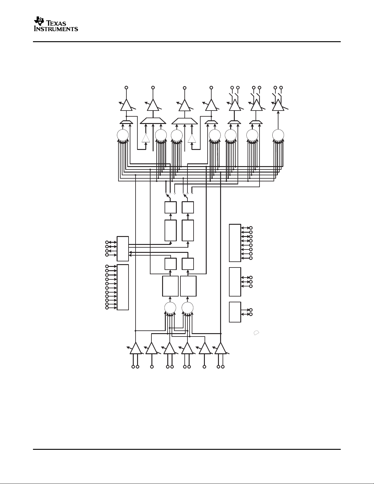
The record path of the TLV320AIC33 contains
integrated microphone bias, digitally controlled stereo
microphone preamplifier, and automatic gain control
(AGC), with mix/mux capability among the multiple
analog inputs. The playback path includes mix/mux
capability from the stereo DAC and selected inputs,
through programmable volume controls, to the
various outputs.
The TLV320AIC33 contains four high-power output
drivers as well as three fully differential output
drivers. The high-power output drivers are capable of
driving a variety of load configurations, including up
to four channels of single-ended 16- Ω headphones
using ac-coupling capacitors, or stereo 16- Ω
headphones in a capacitorless output configuration.
In addition, pairs of drivers can be used to drive 8- Ω
speakers in a BTL configuration at 500 mW per
channel.
Generation
• Control Bus Selectable SPI or I2C
• Audio Serial Data Bus Supports I2S,
Left/Right-Justified, DSP, and TDM Modes
• Alternate Serial PCM/I
2
S Data Bus for Easy
Connection to Bluetooth™ Module
• Digital Microphone Input Support
The stereo audio DAC supports sampling rates from
8 kHz to 96 kHz and includes programmable digital
filtering in the DAC path for 3D, bass, treble,
midrange effects, speaker equalization, and
de-emphasis for 32-kHz, 44.1-kHz, and 48-kHz
rates. The stereo audio ADC supports sampling rates
from 8 kHz to 96 kHz and is preceded by
programmable gain amplifiers providing up to
• Extensive Modular Power Control +59.5-dB analog gain for low-level microphone
• Power Supplies:
inputs.
– Analog: 2.7 V–3.6 V.
– Digital Core: 1.525 V–1.95 V
Please be aware that an important notice concerning availability, standard warranty, and use in critical applications of Texas
Instruments semiconductor products and disclaimers thereto appears at the end of this data sheet.
MIcroStar Junior is a trademark of Texas Instruments.
Bluetooth is a trademark of Bluetooth SIG, Inc..
PRODUCTION DATA information is current as of publication date.
Products conform to specifications per the terms of the Texas
Instruments standard warranty. Production processing does not
necessarily include testing of all parameters.
Copyright © 2006, Texas Instruments Incorporated

www.ti.com
TLV320AIC33
SLAS480A – JANUARY 2006 – REVISED JULY 2006
DESCRIPTION (CONTINUED)
The serial control bus supports SPI or I2C protocols, while the serial audio data bus is programmable for I2S,
left/right-justified, DSP, or TDM modes. A highly programmable PLL is included for flexible clock generation and
support for all standard audio rates from a wide range of available MCLKs, varying from 512 kHz to 50 MHz,
with special attention paid to the most popular cases of 12-MHz, 13-MHz, 16-MHz, 19.2-MHz, and 19.68-MHz
system clocks.
The TLV320AIC33 operates from an analog supply of 2.7 V–3.6 V, a digital core supply of 1.525 V–1.95 V, and
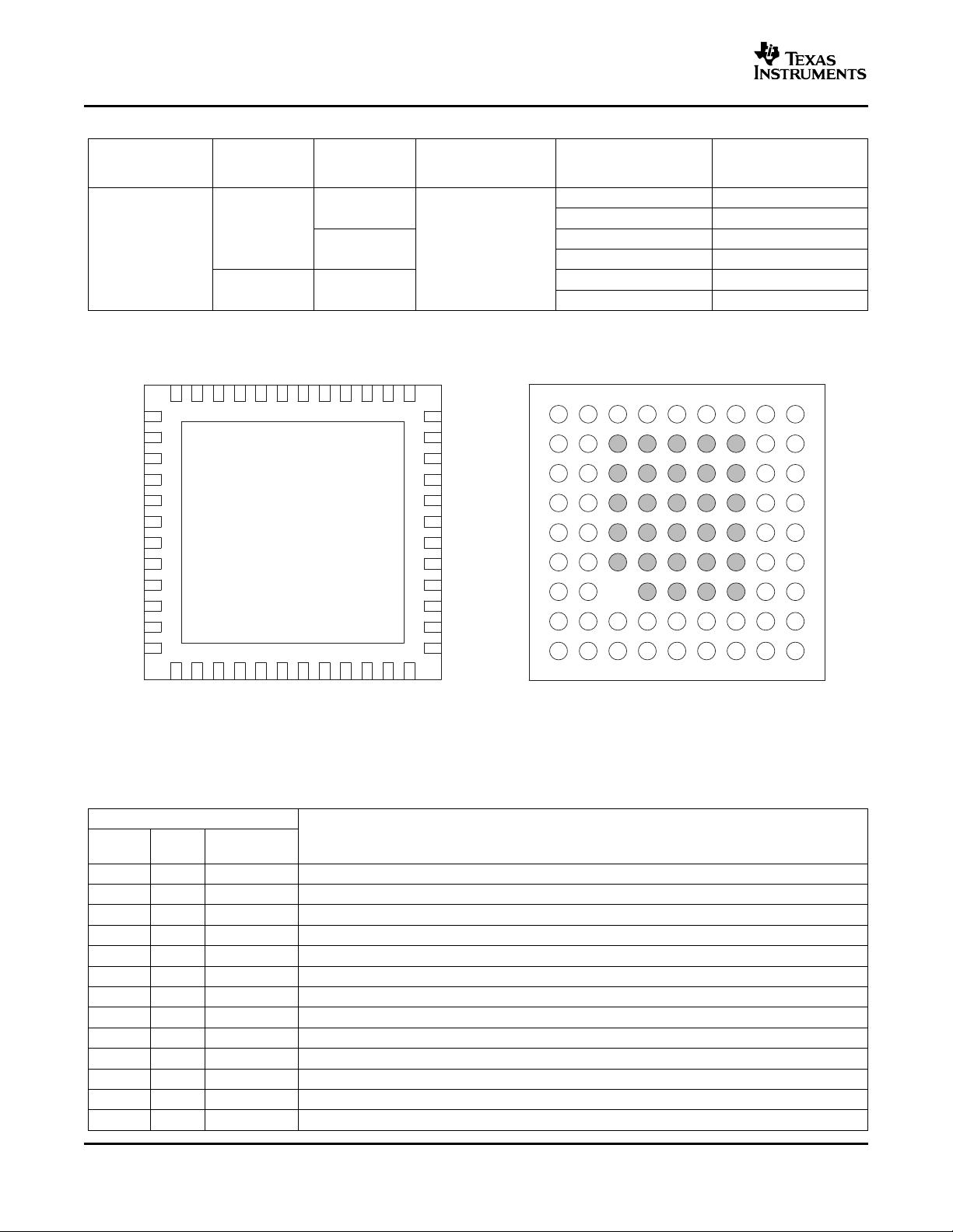
a digital I/O supply of 1.1 V–3.6 V. The device is available in 5 × 5-mm, 80-ball MIcroStar Junior™ BGA and 7 ×
7-mm, 48-lead QFN.
2
Submit Documentation Feedback
www.ti.com
LINE_OUT_L+
LINE_OUT_L−
LINE_OUT_R+
LINE_OUT_R−
MONO_OUT+
MONO_OUT
−
HPR+
HPL−/HPL COM
HPL+
MIC2/LINE2L+
MIC2/LINE2L−
MIC1/LINE1L+
MIC1/LINE1L−
MIC1/LINE1R+
MIC1/LINE1R−
MIC3/LINE3R
MIC3/LINE3L
PGA
0/+59.5dB
0.5dB
steps
ADC
ADC
AudioSerial
Bus
DAC
L
DAC
R
DIN
DOUT
BCLK
WCLK
SPI/I2CSerialControl
Bus
SELECT
CSEL/I2C _ADR0
SCLK/I2C_ADR1
MOSI/GPIO
MISO/GPIO
AudioClock
Generation
MCLK
GPIO_1
GPIO_2
Bias/
Reference
MICBIAS
VoltageSupplies
AVDD_DAC
AVSS_DAC
DRVDD
DRVSS
DVDD
DVSS
IOVDD
VolumeCtl
&Effects
VolumeCtl
&Effects
DRVDD
DRVSS
SCL/GPIO
SDA/GPIO
AVDD_ADC
AVSS_ADC
RESETB
MICDET
MIC2/LINE2R−
MIC2/LINE2R+
+
+
VCM
+
+
+
HPR−/HPRCOM/
SPKFC
+
VCM
+
PGA
0/+59.5dB
0.5dB
steps
+
+
TLV320AIC33
SLAS480A – JANUARY 2006 – REVISED JULY 2006
SIMPLIFIED BLOCK DIAGRAM
Submit Documentation Feedback
3
www.ti.com
A
1 2 3 4
5
6
7
8 9
B
C
D
E
F
G
H
J
48−leadQFNPackage(Bottomview) 5x5mm80−BallBGAPackage(BottomView)
48
1
12
13
24
25
36
37
(Nottoscale)
TLV320AIC33
SLAS480A – JANUARY 2006 – REVISED JULY 2006
PACKAGING/ORDERING INFORMATION
PRODUCT PACKAGE DESIGNATOR TEMPERATURE NUMBER MEDIA, QUANTITY
BGA-80
TLV320AIC33 GQE –40 ° C to 85 ° C
QFN-48 RGZ
PACKAGE OPERATING ORDERING TRANSPORT
RANGE
ZQE
TLV320AIC33IZQE Trays, 360
TLV320AIC33IZQER Tape and Reel, 3000
TLV320AIC33IGQE Trays, 360
TLV320AIC33IGQER Tape and Reel, 3000
TLV320AIC33IRGZT Tape and Reel, 250
TLV320AIC33IRGZR Tape and Reel, 2000
PIN ASSIGNMENTS
TERMINAL FUNCTIONS
TERMINAL
BGA
BALL
A2 13 MICBIAS Microphone Bias Voltage Output
A1 14 MIC3R MIC3 Input (Right or Multifunction)
C2,D2 15 AVSS_ADC Analog ADC Ground Supply, 0 V
B1,C1 16,17 DRVDD ADC Analog and Output Driver Voltage Supply, 2.7 V–3.6 V
D1 18 HPLOUT High-Power Output Driver (Left Plus)
E1 19 HPLCOM High-Power Output Driver (Left Minus or Multifunctional)
E2,F2 20,21 DRVSS Analog Output Driver Ground Supply, 0 V
F1 22 HPRCOM High-Power Output Driver (Right Minus or Multifunctional)
G1 23 HPROUT High-Power Output Driver (Right Plus)
H1 24 DRVDD ADC Analog and Output Driver Voltage Supply, 2.7 V– 3.6 V
J1 25 AVDD Analog DAC Voltage Supply, 2.7 V–3.6 V
G2,H2 26 AVSS_DAC Analog DAC Ground Supply, 0 V
J2 27 MONO_LOP Mono Line Output (Plus)
4
QFN NAME
Submit Documentation Feedback
DESCRIPTION
www.ti.com
SLAS480A – JANUARY 2006 – REVISED JULY 2006
PIN ASSIGNMENTS (continued)
TERMINAL FUNCTIONS (continued)
TERMINAL
BGA
BALL
J3 28 MONO_LOM Mono Line Output (Minus)
J4 29 LEFT_LOP Left Line Output (Plus)
J5 30 LEFT_LOM Left Line Output (Minus)
J6 31 RIGHT_LOP Right Line Output (Plus)
J7 32 RIGHT_LOM Right Line Output (Minus)t
H8 33 RESET Reset
J8 34 GPIO2
J9 35 GPIO1
H9 36 DVDD Digital Core Voltage Supply, 1.525V – 1.95V
G8 37 MCLK Master Clock Inputt
G9 38 BCLK Audio Serial Data Bus Bit Clock (Input/Output)
F9 39 WCLK Audio Serial Data Bus Word Clock (Input/Output)
E9 40 DIN Audio Serial Data Bus Data Input (Input)
F8 41 DOUT Audio Serial Data Bus Data Output (Output)t
D9 42 DVSS Digital Core / I/O Ground Supply, 0V
E8 43 SELECT Control Mode Select Pin (1=SPI, 0=I
C9 44 IOVDD I/O Voltage Supply, 1.1V – 3.6V
B8 45 MFP0 Multifunction pin #0 - SPI Chip Select / GPI / I2C Address Pin #0
B9 46 MFP1 Multifunction pin #1 - SPI Serial Clock / GPI / I2C Address Pin #1S
A8 47 MFP2 Multifunction pin #2 - SPI MISO Slave Serial Data Output / GPOI
A9 48 MFP3 Multifunction pin #3 - SPI MOSI Slave Serial Data Input / GPI / Audio Serial Data Bus Data Input
C8 1 SCL I2C Serial Clock / GPIO
D8 2 SDA I2C Serial Data Input/Output / GPIO
A7 NC No Connect
A6 3 LINE1LP MIC1 or Line1 Analog Input (Left Plus or Multifunction)
A5 4 LINE1LM MIC1 or Line1 Analog Input (Left Minus or Multifunction)I
B7 5 LINE1RP MIC1 or Line1 Analog Input (Right Plus or Multifunction)I
B6 6 LINE1RM MIC1 or Line1 Analog Input (Right Minus or Multifunction)
A4 7 LINE2LP MIC2 or Line2 Analog Input (Left Plus or Multifunction)
B5 8 LINE2LM MIC2 or Line2 Analog Input (Left Minus or Multifunction)I
B4 9 LINE2RP MIC2 or Line2 Analog Input (Right Plus or Multifunction)I
A3 10 LINE2RM MIC2 or Line2 Analog Input (Right Minus or Multifunction)I
B3 11 MIC3L MIC3 Input (Left or Multifunction)
B2 12 MICDET Microphone Detect
QFN NAME
General-Purpose Input/Output #2 (Input/Output) / Digital Microphone Data Input / PLL Clock Input /
Audio Serial Data Bus Bit Clock Input/Output
General-Purpose Input/Output #1 (Input/Output) / PLL/Clock Mux Output / Short Circuit Interrupt /
AGC Noise Flag / Digital Microphone Clock Audio Serial Data Bus Word Clock Input/Output
DESCRIPTION
2
C)
TLV320AIC33
Submit Documentation Feedback
5
www.ti.com
TLV320AIC33
SLAS480A – JANUARY 2006 – REVISED JULY 2006
ABSOLUTE MAXIMUM RATINGS
over operating free-air temperature range (unless otherwise noted)
AVDD to AVSS, DRVDD to DRVSS –0.3 to 3.9 V
AVDD to DRVSS –0.3 to 3.9 V
IOVDD to DVSS –0.3 to 3.9 V
DVDD to DVSS –0.3 to 2.5 V
AVDD to DRVDD –0.1 to 0.1 V
Digital input voltage to DVSS –0.3 V to IOVDD+0.3 V
Analog input voltage to AVSS –0.3 V to AVDD+0.3 V
Operating temperature range -40 to +85 ° C
Storage temperature range -65 to +105 ° C
TJMax Junction temperature 105 ° C
Power dissipation (T
θ
JA
(1) Stresses beyond those listed under absolute maximum ratings may cause permanent damage to the device. These are stress ratings
(2) ESD complicance tested to EIA / JESD22-A114-B and passed.
Thermal impedance , BGA package 63 ° C/W
Thermal impedance, QFN package 38.5 ° C/W
only, and functional operation of the device at these or any other conditions beyond those indicated under recommended operating
conditions is not implied. Exposure to absolute-maximum-rated conditions for extended periods may affect device reliability.
(1) (2)
VALUE UNIT
Max – TA) / θ
J
JA
DISSIPATION RATINGS
(1)
Package Type TA= 25 ° C DERATING TA= 75 ° C TA= 85 ° C
POWER RATING FACTOR POWER RATING POWER RATING
BGA 1.27 W 15.9 mW/ ° C 476 mW 317 mW
QFN 2.08 W 26.0 mW/ ° C 779 mW 519 mW
(1) This data was taken using 2 oz. trace and copper pad that is soldered directly to a JEDEC standard 4-layer 3 in × 3 in PCB.
RECOMMENDED OPERATING CONDITIONS
over operating free-air temperature range (unless otherwise noted)
MIN NOM MAX UNIT
AVDD, Analog supply voltage 2.7 3.3 3.6 V
DRVDD1
(1)
/2
(1)
DVDD
IOVDD
V
I
T
A
(1) Analog voltage values are with respect to AVSS1, AVSS2, DRVSS; digital voltage values are with respect to DVSS.
Digital core supply voltage 1.525 1.8 1.95 V
(1)
Digital I/O supply voltage 1.1 1.8 3.6 V
Analog full-scale 0 dB input voltage (DRVDD1 = 3.3 V) 0.707 V
Stereo line-output load resistance 10 k Ω
Stereo headphone-output load resistance 16 Ω
Digital output load capacitance 10 pF
Operating free-air temperature –40 85 ° C
RMS
6
Submit Documentation Feedback
www.ti.com
SLAS480A – JANUARY 2006 – REVISED JULY 2006
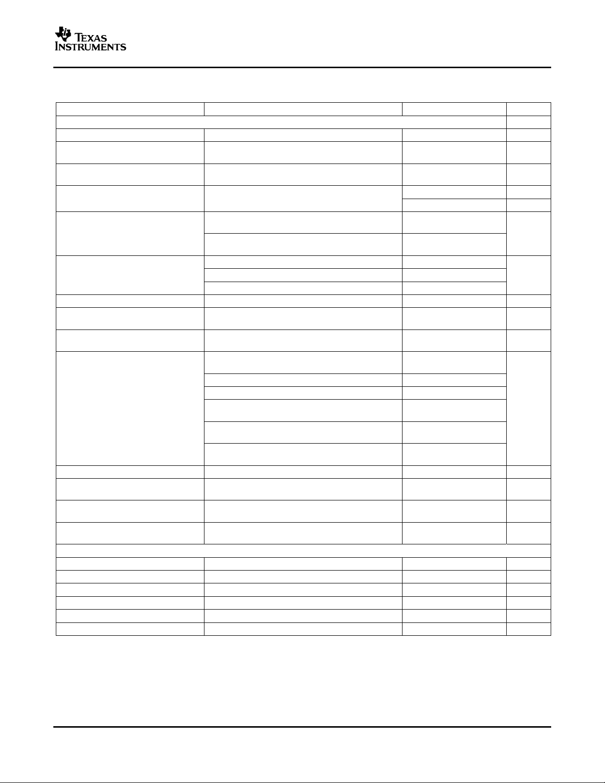
ELECTRICAL CHARACTERISTICS
At 25 ° C, AVDD, DRVDD, IOVDD = 3.3 V, DVDD = 1.8 V, Fs = 48-kHz, 16-bit audio data (unless otherwise noted)
PARAMETER TEST CONDITIONS MIN TYP MAX UNIT
AUDIO ADC
Input signal level (0-dB) Single-ended input 0.707 V
Signal-to-noise ratio, Fs = 48 kHz, 0 dB PGA gain, MIC1/LINE1 inputs
A-weighted
Dynamic range, A-weighted
THD Total harmonic distortion
Power supply rejection ratio dB
ADC channel separation 1 kHz, –2 dB MIC2L to MIC2R –99 dB
ADC gain error 1 kHz input, 0 dB PGA gain 0.7 dB
ADC programmable gain
amplifier maximum gain
ADC programmable gain
amplifier step size
Input resistance k Ω
Input capacitance MIC1/LINE1 inputs 10 pF
Input level control minimum
attenuation setting
Input level control maximum
attenuation setting
Input level control attenuation
step size
ADC DIGITAL DECIMATION FILTER, Fs = 48 kHz
Filter gain from 0 to 0.39 Fs ± 0.1 dB
Filter gain at 0.4125 Fs –0.25 dB
Filter gain at 0.45 Fs –3 dB
Filter gain at 0.5 Fs –17.5 dB
Filter gain from 0.55 Fs to 64 Fs –75 dB
Filter group delay 17/Fs Sec
(1) (2)
selected and AC-shorted to ground
Fs = 48 kHz, 1-kHz –60 dB full-scale input applied at
(1) (2)
MIC1/LINE1 inputs, 0-dB PGA gain
Fs = 48 kHz, 1-kHz –2dB full-scale input applied at
MIC1/LINE1 inputs, 0-dB PGA gain
234 Hz, 100 mVpp on AVDD, DRVDD, single-ended
input
234 Hz, 100mVpp on AVDD, DRVDD, differential
input
1 kHz, –2 dB MIC3L to MIC3R –80
1 kHz, –2 dB MIC1L to MIC1R –-73
1-kHz input tone, R
MIC1/LINE1 inputs, routed to single ADC
Input mix attenuation = 0 dB
MIC2/LINE2 inputs, input mix attenuation = 0 dB 20
MIC3/LINE3 inputs, input mix attenuation = 0 dB 20
MIC1/LINE1 inputs,
input mix attenuation = –12 dB
MIC2/LINE2 inputs,
input mix attenuation = –12 dB
MIC3/LINE3 inputs,
input mix attenuation = –12 dB
< 50 Ω 59.5 dB
SOURCE
80 92 dB
–90 –75 dB
0.003% 0.017%
0.5 dB
1.5 dB
TLV320AIC33
RMS
92 dB
46
68
20
80
80
80
0 dB
12 dB
(1) Ratio of output level with 1-kHz full-scale sine wave input, to the output level with the inputs short circuited, measured A-weighted over a
20-Hz to 20-kHz bandwidth using an audio analyzer.
(2) All performance measurements done with 20-kHz low-pass filter and, where noted, A-weighted filter. Failure to use such a filter may
result in higher THD+N and lower SNR and dynamic range readings than shown in the Electrical Characteristics. The low-pass filter
removes out-of-band noise, which, although not audible, may affect dynamic specification values.
Submit Documentation Feedback
7
www.ti.com
TLV320AIC33
SLAS480A – JANUARY 2006 – REVISED JULY 2006
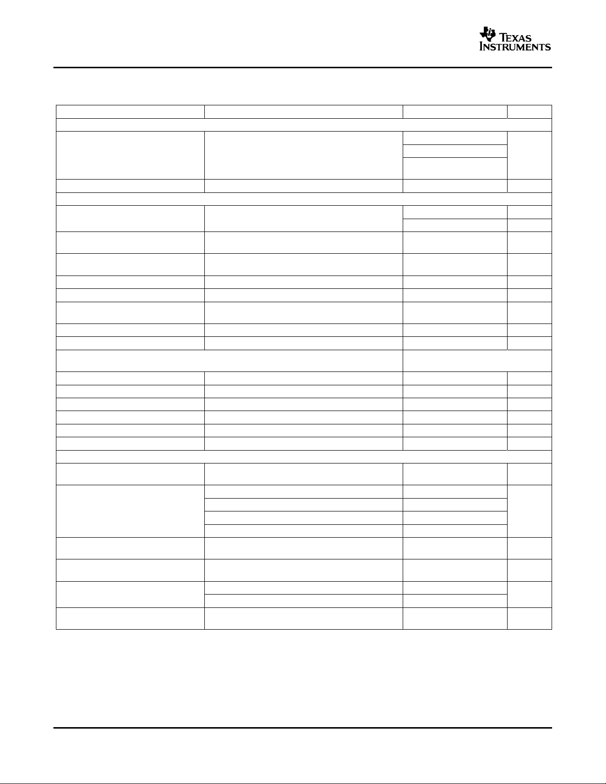
ELECTRICAL CHARACTERISTICS (continued)
At 25 ° C, AVDD, DRVDD, IOVDD = 3.3 V, DVDD = 1.8 V, Fs = 48-kHz, 16-bit audio data (unless otherwise noted)
PARAMETER TEST CONDITIONS MIN TYP MAX UNIT
MICROPHONE BIAS
Bias voltage Programmable settings, load = 750 Ω V
Current sourcing 2.5 V setting 4 mA
AUDIO DAC Differential Line output, load = 10 k Ω , 50 pF
Full-scale differential output 0-dB gain to line outputs. DAC output common-mode
voltage setting = 1.35 V, output level control gain = 0-dB
Signal-to-noise ratio, Fs = 48 kHz, 0-dB gain to line outputs, zero signal
A-weighted
Dynamic range, A-weighted 100 dB
(3)
applied, referenced to full-scale input level
Fs = 48 kHz, 0-dB gain to line outputs,
1 kHz –60 dB signal applied
Total harmonic distortion Fs = 48 kHz, 1 kHz 0 dB input signal applied –93 –75 dB
Power supply rejection ratio 234 Hz, 100 mVpp on AVDD, DRVDD1/2 81 dB
DAC channel separation (left to
right)
1-kHz, 0-dB –100 dB
DAC interchannel gain mismatch 1 kHz input, 0dB gain 0.1 dB
DAC Gain Error 1 kHz input, 0dB gain –0.4 dB
DAC DIGITAL INTERPOLATION
FILTER
Fs = 48-kHz
Passband High-pass filter disabled 0.45 × Fs Hz
Passband ripple High-pass filter disabled ± 0.06 dB
Transition band 0.45 × Fs 0.55 × Fs Hz
Stopband 0.55 × Fs 7.5 × Fs Hz
Stopband attenuation 65 dB
Group delay 21/Fs Sec
STEREO HEADPHONE DRIVER AC-coupled output configuration
0-dB full-scale output voltage 0.707 V
0-dB gain to high power outputs. Output
common-mode voltage setting = 1.35 V
(4)
First option 1.35
Programmable output common
mode voltage (applicable to Line V
Outputs also)
Second option 1.50
Third option 1.65
Fourth option 1.8
Maximum programmable output
level control gain
Programmable output level
control gain step size
P
Maximum output power mW
O
Signal-to-noise ratio,
A-weighted
(5)
RL= 32 Ω 15
RL= 16 Ω 30
2.25 2.5 2.75
90 100 dB
2.0
AVDD-
0.2
1.414 V
4.0 V
9 dB
1 dB
94 dB
RMS
PP
RMS
(3) Unless otherwise noted, all measurements use output common-mode voltage setting of 1.35 V, 0-dB output level control gain, 16- Ω
single-ended load.
(4) Unless otherwise noted, all measurements use output common-mode voltage setting of 1.35 V, 0-dB output level control gain, 16- Ω
single-ended load.
(5) Ratio of output level with a 1-kHz full-scale input, to the output level playing an all-zero signal, measured A-weighted over a 20-Hz to
20-kHz bandwidth.
8
Submit Documentation Feedback
www.ti.com
SLAS480A – JANUARY 2006 – REVISED JULY 2006
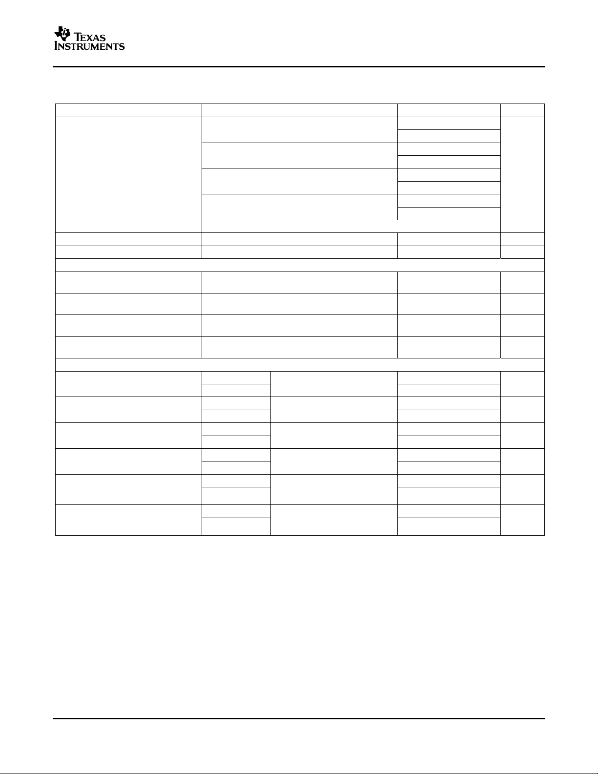
ELECTRICAL CHARACTERISTICS (continued)
At 25 ° C, AVDD, DRVDD, IOVDD = 3.3 V, DVDD = 1.8 V, Fs = 48-kHz, 16-bit audio data (unless otherwise noted)
PARAMETER TEST CONDITIONS MIN TYP MAX UNIT
1-kHz output, PO= 5 mW, RL= 32 Ω
1-kHz output, PO= 10 mW, RL= 32 Ω
Total harmonic distortion dB%
1-kHz output, PO= 10 mW, RL= 16 Ω
1-kHz output, PO= 20 mW, RL= 16 Ω
Channel separation 1 kHz, 0 dB input 90 dB
Power supply rejection ratio 217 Hz, 100 mVpp on AVDD, DRVDD1/2 48 dB
Mute attenuation 1-kHz output 107 dB
DIGITAL I/O
V
Input low level IIL= +5- µ A –0.3 V
IL
V
Input high level
IH
V
Output low level IIH= 2 TTL loads V
OL
V
Output high level IOH= 2 TTL loads V
OH
(6)
IIH= +5- µ A V
0.7 ×
IOVDD
0.8 ×
IOVDD
SUPPLY CURRENT Fs = 48-kHz
Stereo line playback mA
Mono record Fs = 48-kHz, PLL and AGC off mA
Stereo record Fs = 48-kHz, PLL and AGC off mA
PLL mA
AVDD+DRVDD 3.0
DVDD 2.0
AVDD+DRVDD 2.2
DVDD 1.1
AVDD+DRVDD 4.2
DVDD 1.3
AVDD+DRVDD 1.2
DVDD 1
Fs = 48-kHz, PLL off, headphone
drivers off, DAC direct mode
Additional power consumed when
PLL is powered
AVDD+DRVDD LINE2LP/RP only routed to stereo 5.6
Headphone amplifier single-ended headphones, DAC mA
DVDD 0
and PLL off, no signal applied
AVDD+DRVDD All supply voltages applied, all 0.1
Power down blocks programmed in lowest µ A
DVDD 0.5
power state
–77
0.014
–76
0.016
–73
0.022
–71
0.028
TLV320AIC33
0.3 ×
IOVDD
0.1 ×
IOVDD
(6) When IOVDD < 1.6V, minimum VIH is 1.1V.
Submit Documentation Feedback
9
www.ti.com
WCLK
BCLK
SDOUT
SDIN
td(WS)
td(DO-WS)
td(DO-BCLK)
ts(DI)
th(DI)
BCLK
WCLK
SDOUT
SDIN
td(WS)
td(WS)
td(DO-BCLK)
th(DI)
ts(DI)
TLV320AIC33
SLAS480A – JANUARY 2006 – REVISED JULY 2006
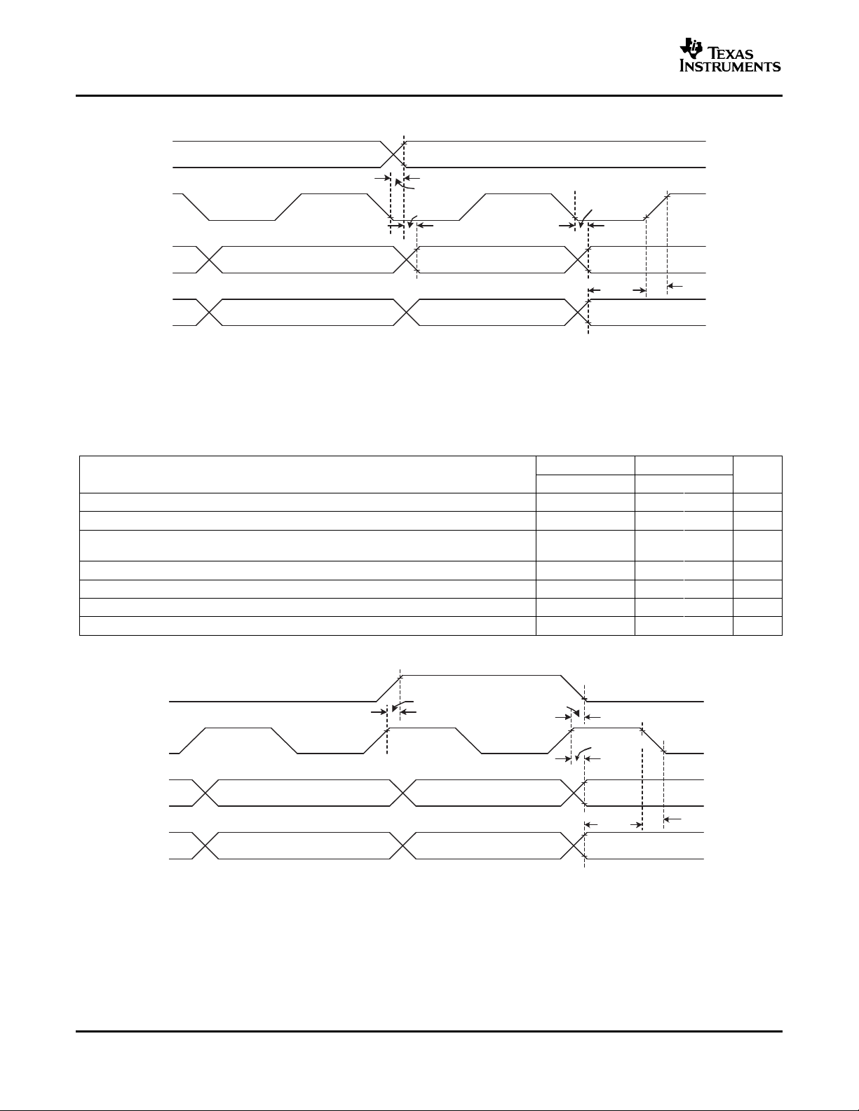
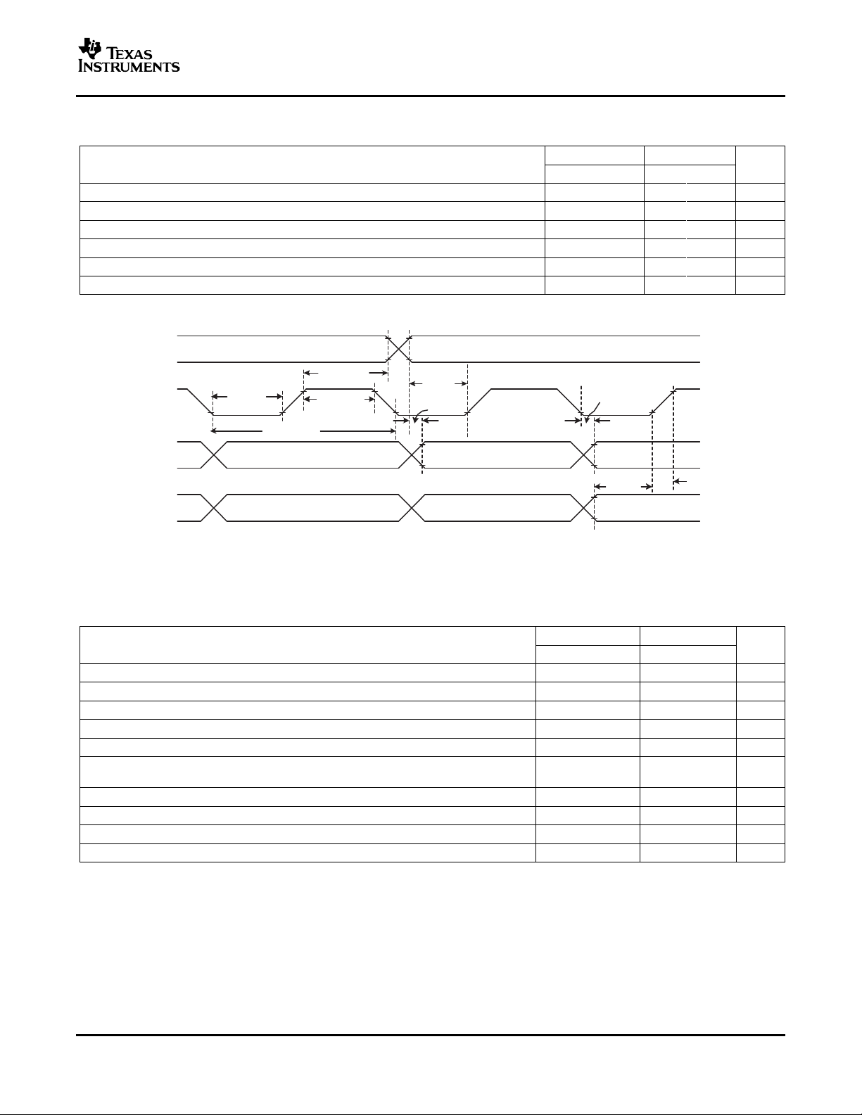
AUDIO DATA SERIAL INTERFACE TIMING DIAGRAM
Figure 1. I2S/LJF/RJF Timing in Master Mode
TIMING CHARACTERISTICS
(1)
All specifications typical at 25 ° C, DVDD = 1.8 V
PARAMETER UNIT
td(WS) ADWS/WCLK delay time 50 15 ns
td(DO-WS) ADWS/WCLK to DOUT delay time 50 20 ns
t
d
(DO-BCLK)
ts(DI) DIN setup time 10 6 ns
th(DI) DIN hold time 10 6 ns
t
r
t
f
(1) All timing specifications are measured at characterization but not tested at final test.
BCLK to DOUT delay time 50 15 ns
Rise time 30 10 ns
Fall time 30 10 ns
IOVDD = 1.1 V IOVDD = 3.3 V
MIN MAX MIN MAX
Figure 2. DSP Timing in Master Mode
10
Submit Documentation Feedback
www.ti.com
WCLK
BCLK
SDOUT
SDIN
td(DO-WS)
tH(BCLK)
ts(DI)
th(DI)
th(WS)
ts( WS)
tL(BCLK)
td(DO-BCLK)
tP(BCLK)
TLV320AIC33
SLAS480A – JANUARY 2006 – REVISED JULY 2006
TIMING CHARACTERISTICS
All specifications typical at 25 ° C, DVDD = 1.8 V
td(WS) ADWS/WCLK delay time 50 15 ns
td(DO-BCLK) BCLK to DOUT delay time 50 15 ns
ts(DI) DIN setup time 10 6 ns
th(DI) DIN hold time 10 6 ns
t
r
t
f
(1) All timing specifications are measured at characterization but not tested at final test.
Rise time 30 10 ns
Fall time 30 10 ns
(1)
PARAMETER UNIT
IOVDD = 1.1 V IOVDD = 3.3 V
MIN MAX MIN MAX
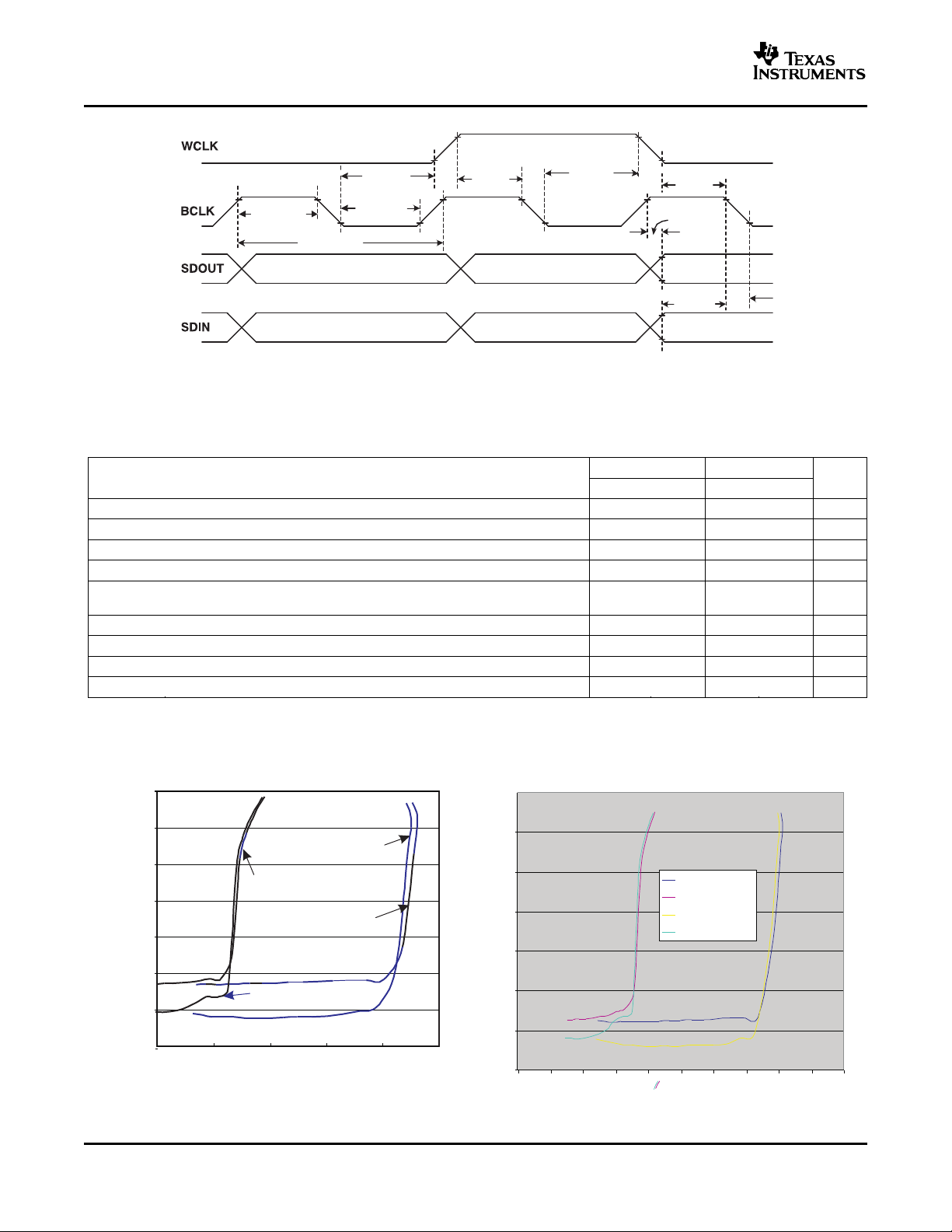
Figure 3. I2S/LJF/RJF Timing in Slave Mode
TIMING CHARACTERISTICS
All specifications typical at 25 ° C, DVDD = 1.8 V
tH(BCLK) BCLK high period 70 35 ns
tL(BCLK) BCLK low period 70 35 ns
ts(WS) ADWS/WCLK setup time 10 6 ns
th(WS) ADWS/WCLK hold time 10 6 ns
td(DO-WS) ADWS/WCLK to DOUT delay time (for LJF Mode only) TBD TBD ns
t
d
(DO-BCLK)
ts(DI) DIN setup time 10 6 ns
th(DI) DIN hold time 10 6 ns
t
r
t
f
(1) All timing specifications are measured at characterization but not tested at final test.
BCLK to DOUT delay time 50 20 ns
Rise time 8 4 ns
Fall time 8 4 ns
(1)
PARAMETER UNIT
IOVDD = 1.1 V IOVDD = 3.3 V
MIN MAX MIN MAX
Submit Documentation Feedback
11
www.ti.com
th(WS)
ts(WS)
th(WS)
ts(WS)
td(DO-BCLK)
t s ( D I )
tL(BCLK)
tH(BCLK)
tP(BCLK)
-90
-80
-70
-60
-50
-40
-30
-20
0.015 0.02 0.025 0.03 0.035 0.04
Capless,VDD=3.6V
Capless,VDD=2.7V
AC-Coupled,VDD=3.6V
AC-Coupled,VDD=2.7V
TotalHarmonic Distortion -d
B
Power-W
-90
-80
-70
-60
-50
-40
-30
-20
0.005 0.007 0.009 0.011 0.013 0.015 0.017 0.019 0.021 0.023 0.025
Power, W
THD,dB
AC-Coupled, VDD=3.6V
AC-Coupled, VDD=2.7V
Capless,VDD=3.6V
Capless,VDD=2.7V
TLV320AIC33
SLAS480A – JANUARY 2006 – REVISED JULY 2006
Figure 4. DSP Timing in Slave Mode
TIMING CHARACTERISTICS
(1)
All specifications typical at 25 ° C, DVDD = 1.8 V
PARAMETER UNIT
tH(BCLK) BCLK high period 70 35 ns
tL(BCLK) BCLK low period 70 35 ns
ts(WS) ADWS/WCLK setup time 10 8 ns
th(WS) ADWS/WCLK hold time 10 8 ns
t
d
(DO-BCLK)
BCLK to DOUT delay time 50 20 ns
ts(DI) DIN setup time 10 6 ns
th(DI) DIN hold time 10 6 ns
t
r
t
f
Rise time 8 4 ns
Fall time 8 4 ns
(1) All timing specifications are measured at characterization but not tested at final test.
IOVDD = 1.1 V IOVDD = 3.3 V
MIN MAX MIN MAX
TYPICAL CHARACTERISTICS
12
Figure 5. Headphone Power vs THD, 16 Ω Load Figure 6. Headphone Power vs THD, 32 Ω Load
Submit Documentation Feedback
www.ti.com
-140.00
-120.00
-100.00
-80.00
-60.00
-40.00
-20.00
0.00
0 1 2 3 4 5 6 7 8 9 10 11 12 13 14 15 16 17 18 19 20
Frequency-kHz
dB
-140
-120
-100
-80
-60
-40
-20
0
0 1 2 3 4 5 6 7 8 9 10 11 12 13 14 15 16 17 18 19 20
Frequency-kHz
dB
TYPICAL CHARACTERISTICS (continued)
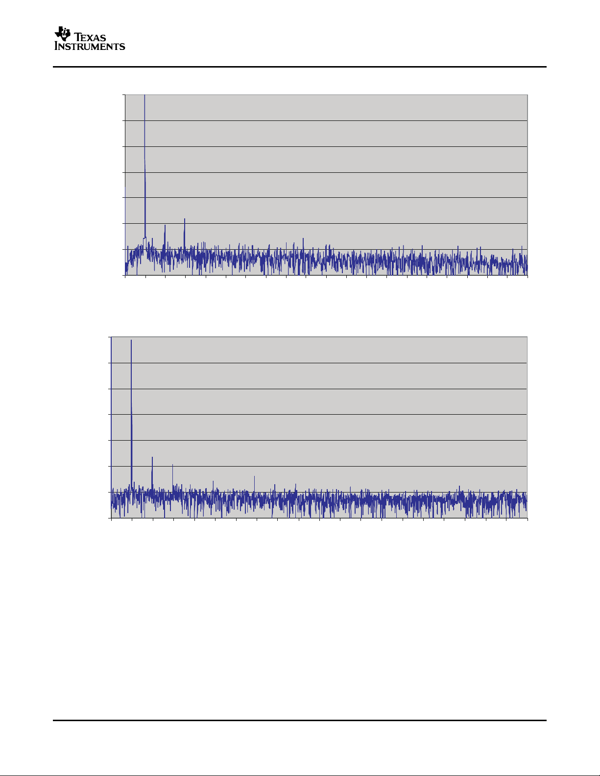
Figure 7. DAC to Line Output FFT Plot
TLV320AIC33
SLAS480A – JANUARY 2006 – REVISED JULY 2006
Figure 8. Line Input to ADC FFT Plot
Submit Documentation Feedback
13
www.ti.com
VDD=3.3V VDD=3.6V
VDD=2.7V
-9 0 .0 0
-8 0 .0 0
-7 0 .0 0
-6 0 .0 0
-5 0 .0 0
-4 0 .0 0
-3 0 .0 0
-2 0 .0 0
-1 0 .0 0
0.1 0 0 .2 0 0.30 0.40 0.50 0. 6 0
Power-W
TH D
2 6
2 8
3 0
3 2
3 4
3 6
3 8
0 1 0 2 0 30 4 0 50 6 0
PGA GainSetting-dB
SNR-dB
TLV320AIC33
SLAS480A – JANUARY 2006 – REVISED JULY 2006
TYPICAL CHARACTERISTICS (continued)
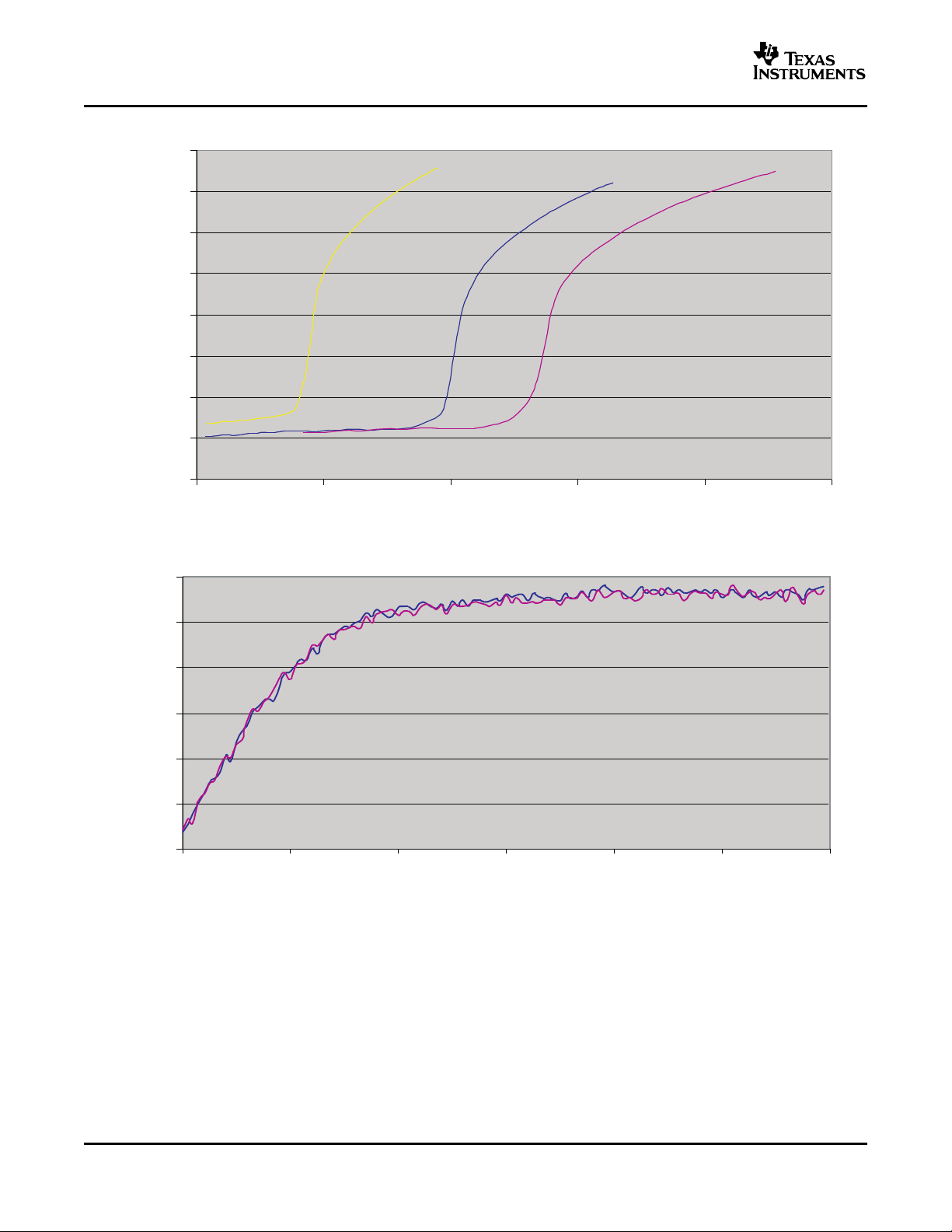
Figure 9. Speaker Power vs THD, 8 Ω Load
Figure 10. ADC SNR vs PGA Gain Setting, –65 dBFS Input
14
Submit Documentation Feedback
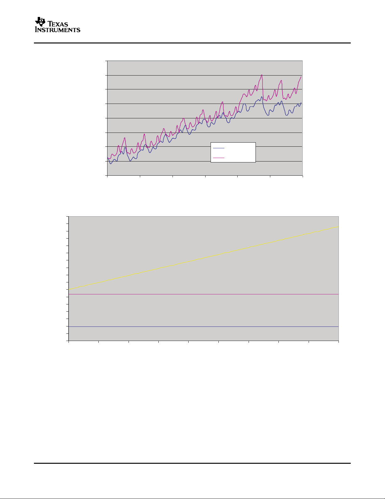
www.ti.com
0.40
0.50
0.60
0.70
0.80
0.90
1.00
1.10
1.20
0 10 20 30 40 50 60
PGA GainSetting-dB
GainError-dB
Left ADC
Right ADC
MICBIAS=2.0V
MICBIAS=2.5V
MICBIAS=AVDD
1.8
1.9
2
2.1
2.2
2.3
2.4
2.5
2.6
2.7
2.8
2.9
3
3.1
3.2
3.3
3.4
3.5
2.7 2.8 2.9 3 3. 1 3.2 3. 3 3.4 3.5 3.6
AVDD-V
Micbias-V
TYPICAL CHARACTERISTICS (continued)
Figure 11. ADC Gain Error vs PGA Gain Setting
TLV320AIC33
SLAS480A – JANUARY 2006 – REVISED JULY 2006
Figure 12. MICBIAS Output Voltage vs AVDD
Submit Documentation Feedback
15
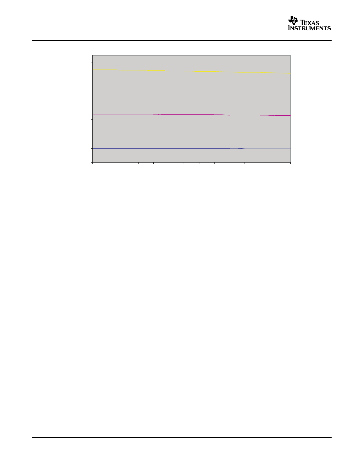
www.ti.com
MICBIAS=2.0V
MICBIAS=2.5V
MICBIAS=AVDD
1.8
2
2.2
2.4
2.6
2.8
3
3.2
-45 -35 -25 -15 -5 5 15 25 35 45 55 65 75 85
Temp-C
Micbias-V
TLV320AIC33
SLAS480A – JANUARY 2006 – REVISED JULY 2006
TYPICAL CHARACTERISTICS (continued)
Figure 13. MICBIAS Output Voltage vs Ambient Temperature
16
Submit Documentation Feedback
www.ti.com
AIC33
LINE2LP
LINE2LM
LINE1LP
LINE1LM
LINE1RP
LINE1RM
MIC3L
MICBIAS
A
AVDD_DAC
AVSS_DAC
DRVDD
DRVSS
PVDD
DVSS
IOVDD
DRVDD
DRVSS
AVDD_ADC
AVSS_ADC
A
D
1.525−1.95V
IOVDD
(1.1−3.3V)
LEFT_LOP
LEFT_LOM
RIGHT_ROP
RIGHT_ROM
HPROUT
HPLCOM
HPRCOM
MICDET
A
AVDD
(2.7V−3.6V)
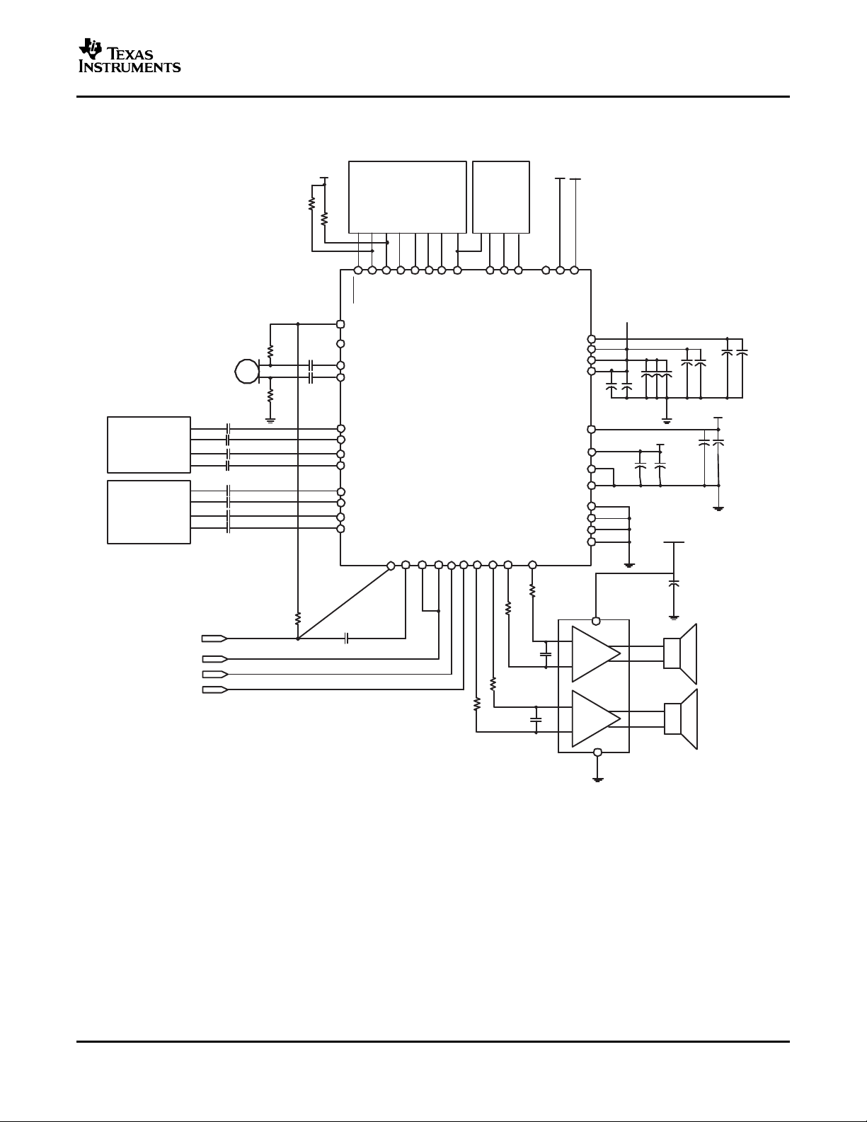
TLV320AIC33 Connections
Stereo Speakers with Multiple Audio Processors
MIC3R
HPLOUT
HEADSET_MIC
HEADSET_GND
HEADSET_SPKR_R
HEADSET_SPKR_L
A
A
VBAT
PVSS
DVDD
Earjack mic
and
headset
speakers
(capless)
Handset Mic
Analog Baseband /
Modem
MONO_LOP
MONO_LOM
LINE2RP
LINE2RM
Line In /
FM
Multimedia
Processor
DOUT
MFP0
BCLK
DIN
MCLK
GPIO1
GPIO2
SCL
SDA
WCLK
MFP2
MFP1
RESET
MFP3
SELECT
DBB /
Modem
Rp
R
p
IOVDD
I2C ADDRESS
TPA2012D2 Class−D Spkr Amp
1 kΩ
1 kΩ
0.47 µF
0.47 µF
0.47 µF
0.47 µF
2 kΩ
560
Ω
560
Ω
560
Ω
4700 pF
4700 pF
560
Ω
µF
µFµF
µF
µF
µF
µF
µF
µF
µF
µF
µF
µFµF
TLV320AIC33
SLAS480A – JANUARY 2006 – REVISED JULY 2006
TYPICAL CHARACTERISTICS (continued)
TYPICAL CIRCUIT CONFIGURATION
Figure 14. Typical Connections for Capless Headphone and External Speaker Amp
Submit Documentation Feedback
17
www.ti.com
RA(6) RA(5) RA(0) D(7) D(6) D(0)
7−bit Register Address Write 8−bit Register Data
/SS
SCLK
MOSI
MISO
TLV320AIC33
SLAS480A – JANUARY 2006 – REVISED JULY 2006
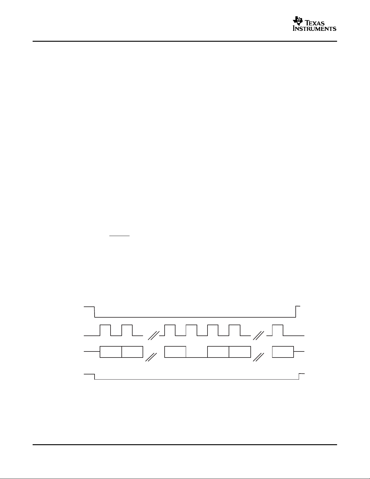
OVERVIEW
The TLV320AIC33 is a highly flexible, low power, stereo audio codec with extensive feature integration, intended
for applications in smartphones, PDAs, and portable computing, communication, and entertainment applications.
Available in a 5x5mm 80-ball BGA (with 51 balls actually used) and 7x7mm 48-lead QFN, the product integrates
a host of features to reduce cost, board space, and power consumption in space-constrained, battery-powered,
portable applications.
The TLV320AIC33 consists of the following blocks:
• Stereo audio multi-bit delta-sigma DAC (8 kHz – 96 kHz)
• Stereo audio multi-bit delta-sigma ADC (8 kHz – 96 kHz)
• Programmable digital audio effects processing (3-D, bass, treble, mid-range, EQ, de-emphasis)
• Six audio inputs
• Four high-power audio output drivers (headphone/speaker drive capability)
• Three fully differential line output drivers
• Fully programmable PLL
• Headphone/headset jack detection with interrupt
Communication to the TLV320AIC33 for control is pin-selectable (using the SELECT pin) as either SPI or I2C.
The SPI interface requires that the Slave Select signal (MFP0) be driven low to communicate with the
TLV320AIC33. Data is then shifted into or out of the TLV320AIC33 under control of the host microprocessor,
which also provides the serial data clock. The I2C interface supports both standard and fast communication
modes, and also enables cascading of up to four multiple codecs on the same I2C bus through the use of two
pins for addressing (MFP0, MFP1).
HARDWARE RESET
The TLV320AIC33 requires a hardware reset after power-up for proper operation. After all power supplies are at
their specified values, the RESET pin must be driven low for at least 10 ns. If this reset sequence is not
performed, the 'AIC33 may not respond properly to register reads/writes.
DIGITAL CONTROL SERIAL INTERFACE
The TLV320AIC33 control interface supports SPI or I2C communication protocols, with the protocol selectable
using the SELECT pin. For SPI, SELECT should be tied high; for I2C, SELECT should be tied low. It is not
recommended to change the state of SELECT during device operation.
SPI CONTROL MODE
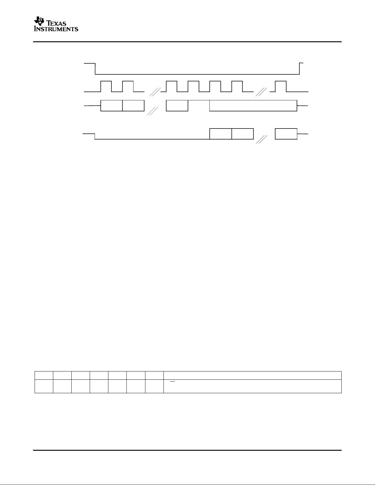
Figure 15. SPI Write
18
Submit Documentation Feedback
www.ti.com
RA(6) RA(5) RA(0)
D(7) D(6) D(0)
Read
/SS
SCLK
MOSI
MISO
DON’T CARE
8-Bit Register Data
7-Bit Register Address
TLV320AIC33
SLAS480A – JANUARY 2006 – REVISED JULY 2006
OVERVIEW (continued)
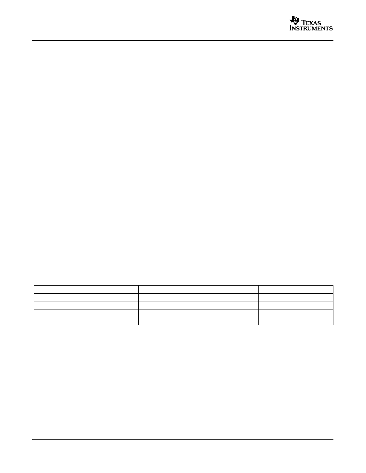
Figure 16. SPI Read
In the SPI control mode, the TLV320AIC33 uses the pins MFP0=SSB, MFP1=SCLK, MFP2=MISO, MFP3=MOSI
as a standard SPI port with clock polarity setting of 0 (typical microprocessor SPI control bit CPOL = 0). The SPI
port allows full-duplex, synchronous, serial communication between a host processor (the master) and peripheral
devices (slaves). The SPI master (in this case, the host processor) generates the synchronizing clock (driven
onto SCLK) and initiates transmissions. The SPI slave devices (such as the TLV320AIC33) depend on a master
to start and synchronize transmissions.
A transmission begins when initiated by an SPI master. The byte from the SPI master begins shifting in on the
slave MOSI pin under the control of the master serial clock (driven onto SCLK). As the byte shifts in on the
MOSI pin, a byte shifts out on the MISO pin to the master shift register.
The TLV320AIC33 interface is designed so that with a clock phase bit setting of 1 (typical microprocessor SPI
control bit CPHA = 1), the master begins driving its MOSI pin and the slave begins driving its MISO pin on the
first serial clock edge. The SSB pin can remain low between transmissions; however, the TLV320AIC33 only
interprets the first 8 bits transmitted after the falling edge of SSB as a command byte, and the next 8 bits as a
data byte only if writing to a register. Reserved register bits should be written to their default values.
SPI COMMUNICATION PROTOCOL
The TLV320AIC33 is entirely controlled by registers. Reading and writing these registers is accomplished by the
use of an 8-bit command, which is sent to the MOSI pin of the part prior to the data for that register. The
command is constructed as shown in the Command Word table. The first 7 bits specify the register address
which is being written or read, from 0 to 127 (decimal). The command word ends with an R/W bit, which
specifies the direction of data flow on the serial bus. In the case of a register write, the R/W bit should be set to
0. A second byte of data is sent to the MOSI pin and contains the data to be written to the register.
Reading of registers is accomplished in similar fashion. The 8-bit command word sends the 7-bit register
address, followed by R/W bit = 1 to signify a register read is occurring,. The 8-bit register data is then clocked
out of the part on the MISO pin during the second 8 SCLK clocks in the frame.
Command Word
Bit 7 Bit 6 Bit 5 Bit 4 Bit 3 Bit 2 Bit 1 Bit 0
ADDR ADDR ADDR ADDR ADDR ADDR ADDR R/ W
6 5 4 3 2 1 0
The register map of the TLV320AIC33 actually consists of multiple pages of registers, with each page containing
128 registers. The register at address zero on each page is used as a page-control register, and writing to this
register determines the active page for the device. All subsequent read/write operations will access the page
that is active at the time, unless a register write is performed to change the active page. Only two pages of
registers are implemented in this product, with the active page defaulting to page 0 upon device reset.
For example, at device reset, the active page defaults to page 0, and thus all register read/write operations for
Submit Documentation Feedback
19
www.ti.com
TLV320AIC33
SLAS480A – JANUARY 2006 – REVISED JULY 2006
addresses 1 to 127 will access registers in page 0. If registers on page 1 must be accessed, the user must write
the 8-bit sequence 0x01 to register 0, the page control register, to change the active page from page 0 to page
1. After this write, it is recommended the user also read back the page control register, to safely ensure the
change in page control has occurred properly. Future read/write operations to addresses 1 to 127 will now
access registers in page 1. When page 0 registers must be accessed again, the user writes the 8-bit sequence
0x00 to register 0, the page control register, to change the active page back to page 0. After a recommended
read of the page control register, all further read/write operations to addresses 1 to 127 will now access page 0
registers again.
Limitation on Register Writing
When writing registers in SPI mode related to the audio output drivers mux, mix, gain configuration, etc., do not
use the auto-increment mode. In addition, between two successive writes to these registers, the host should
keep MFP0 (SPI chip select) high for at least 6.25us, to ensure that the register writes have occurred properly.
CONTINUOUS READ / WRITE OPERATION
The TLV320AIC33 includes the ability to read/write registers continuously, without needing to provide an
address for every register accessed. In SPI mode, a continuous write is executed by transitioning MFP0 (SPI
chip select) low to start the frame, sending the first 8-bit command word to read/write a particular register, and
then sending multiple bytes of register data, intended for the addressed register and those following. A
continuous read is done similarly, with multiple bytes read in from the addressed register and the following
registers on the page. When the MFP0 (SPI chip select) pin is transitioned high again, the frame ends, as does
the continuous read/write operation. A new frame must begin again with a new command word, to start the next
bus transaction.
Note that this continuous read/write operation does not continue past a page boundary. The user should not
attempt to read/write past the end of a page, since this may result in undesirable operation.
I2C CONTROL MODE
The TLV320AIC33 supports the I2C control protocol when the SELECT pin is tied low, using 7-bit addressing
and capable of both standard and fast modes. When in I2C control mode, the TLV320AIC33 can be configured
for one of four different addresses, using the multifunction pins MFP0 and MFP1, which control the two LSBs of
the device address. The 5 MSBs of the device address are fixed as 00110 and cannot be changed, while the
two LSBs are given by MFP1:MFP0. This results in four possible device addresses:
I2C slave device addresses for MFP1, MFP0 settings.
MFP1 MFP0 Device Address
0 0 0011000
0 1 0011001
1 0 0011010
1 1 0011011
I2C is a two-wire, open-drain interface supporting multiple devices and masters on a single bus. Devices on the
I2C bus only drive the bus lines LOW by connecting them to ground; they never drive the bus lines HIGH.
Instead, the bus wires are pulled HIGH by pull-up resistors, so the bus wires are HIGH when no device is driving
them LOW. This way, two devices cannot conflict; if two devices drive the bus simultaneously, there is no driver
contention.
Communication on the I2C bus always takes place between two devices, one acting as the master and the other
acting as the slave. Both masters and slaves can read and write, but slaves can only do so under the direction
of the master. Some I2C devices can act as masters or slaves, but the TLV320AIC33 can only act as a slave
device.
An I2C bus consists of two lines, SDA and SCL. SDA carries data; SCL provides the clock. All data is
transmitted across the I2C bus in groups of eight bits. To send a bit on the I2C bus, the SDA line is driven to the
appropriate level while SCL is LOW (a LOW on SDA indicates the bit is zero; a HIGH indicates the bit is one).
Once the SDA line has settled, the SCL line is brought HIGH, then LOW. This pulse on SCL clocks the SDA bit
into the receivers shift register.
20
Submit Documentation Feedback
www.ti.com
DA(6) DA(0) RA(7) RA(0) D(7) D(0)
Start
(M)
7-bit Device Address
(M)
Write
(M)
Slave
Ack
(S)
8-bit Register Address
(M)
Slave
Ack
(S)
8-bit Register Data
(M)
Stop
(M)
Slave
Ack
(S)
SDA
SCL
(M) => SDA Controlled by Master
(S) => SDA Controlled by Slave
DA(6) DA(0) RA(7) RA(0)
Start
(M)
7-bit Device Address
(M)
Write
(M)
Slave
Ack
(S)
8-bit Register Address
(M)
Slave
Ack
(S)
SDA
SCL
DA(6) DA(0)
7-bit Device Address
(M)
Read
(M)
Slave
Ack
(S)
D(7) D(0)
8-bit Register Data
(S)
Stop
(M)
Master
No Ack
(M)
Repeat
Start
(M)
(M) => SDA Controlled by Master
(S) => SDA Controlled by Slave
TLV320AIC33
SLAS480A – JANUARY 2006 – REVISED JULY 2006
The I2C bus is bidirectional: the SDA line is used both for transmitting and receiving data. When a master reads
from a slave, the slave drives the data line; when a master sends to a slave, the master drives the data line.
Under normal circumstances the master drives the clock line.
Most of the time the bus is idle, no communication is taking place, and both lines are HIGH. When
communication is taking place, the bus is active. Only master devices can start a communication. They do this
by causing a START condition on the bus. Normally, the data line is only allowed to change state while the clock
line is LOW. If the data line changes state while the clock line is HIGH, it is either a START condition or its
counterpart, a STOP condition. A START condition is when the clock line is HIGH and the data line goes from
HIGH to LOW. A STOP condition is when the clock line is HIGH and the data line goes from LOW to HIGH.
After the master issues a START condition, it sends a byte that indicates which slave device it wants to
communicate with. This byte is called the address byte. Each device on an I2C bus has a unique 7-bit address to
which it responds. (Slaves can also have 10-bit addresses; see the I2C specification for details.) The master
sends an address in the address byte, together with a bit that indicates whether it wishes to read from or write to
the slave device.
Every byte transmitted on the I2C bus, whether it is address or data, is acknowledged with an acknowledge bit.
When a master has finished sending a byte (eight data bits) to a slave, it stops driving SDA and waits for the
slave to acknowledge the byte. The slave acknowledges the byte by pulling SDA LOW. The master then sends
a clock pulse to clock the acknowledge bit. Similarly, when a master has finished reading a byte, it pulls SDA
LOW to acknowledge this to the slave. It then sends a clock pulse to clock the bit.
A not-acknowledge is performed by simply leaving SDA HIGH during an acknowledge cycle. If a device is not
present on the bus, and the master attempts to address it, it will receive a not–acknowledge because no device
is present at that address to pull the line LOW.
When a master has finished communicating with a slave, it may issue a STOP condition. When a STOP
condition is issued, the bus becomes idle again. A master may also issue another START condition. When a
START condition is issued while the bus is active, it is called a repeated START condition.
The TLV320AIC33 also responds to and acknowledges a General Call, which consists of the master issuing a
command with a slave address byte of 00H.
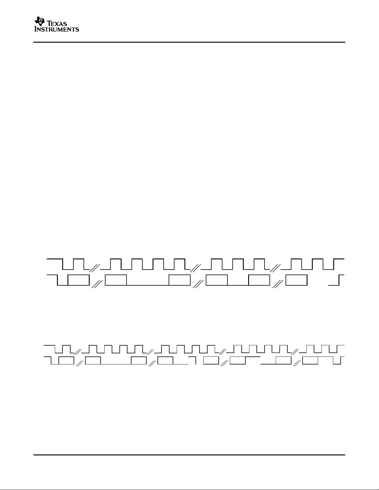
In the case of an I2C register write, if the master does not issue a STOP condition, then the device enters
auto-increment mode. So in the next eight clocks, the data on SDA is treated as data for the next incremental
register.
Figure 17. I2C Write
Figure 18. I2C Read
Submit Documentation Feedback
21
www.ti.com
AudioSerialDataBus
DOUT
GPIO1 GPIO2 MFP3
WCLK BCLK DIN
TLV320AIC33
SLAS480A – JANUARY 2006 – REVISED JULY 2006
Similarly, in the case of an I2C register read, after the device has sent out the 8-bit data from the addressed
register, if the master issues an ACKNOWLEDGE, the slave takes over control of SDA bus and transmit for the
next 8 clocks the data of the next incremental register.
DIGITAL AUDIO DATA SERIAL INTERFACE
Audio data is transferred between the host processor and the TLV320AIC33 via the digital audio data serial
interface, or audio bus. The audio bus on this device is very flexible, including left or right justified data options,
support for I2S or PCM protocols, programmable data length options, a TDM mode for multichannel operation,
very flexible master/slave configurability for each bus clock line, and the ability to communicate with multiple
devices within a system directly.
The data serial interface uses two sets of pins for communication between external devices, with the particular
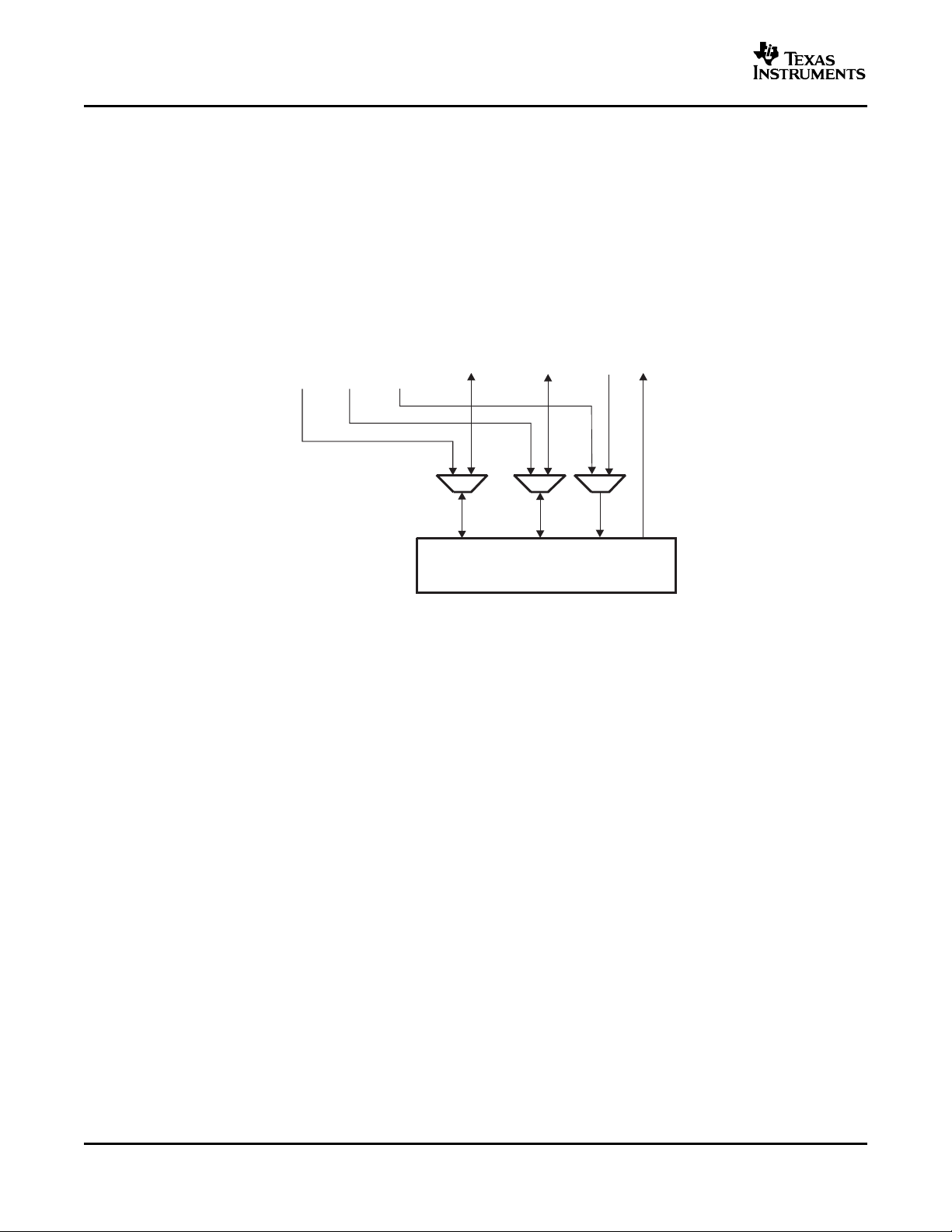
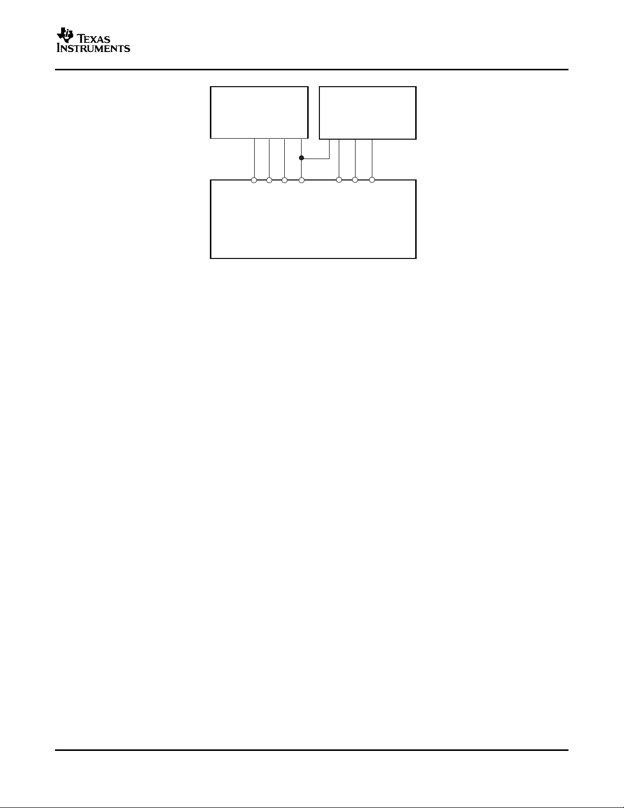
pin used controlled through register programming. This configuration is shown in Figure 19 below.
In cases where MFP3 is needed for a secondary device digital input, the TLV320AIC33 must be used in I2C
mode (when in SPI mode, MFP3 is used as the SPI bus MOSI pin and thus cannot be used here as an alternate
digital input source).
This mux capability allows the TLV320AIC33 to communicate with two separate devices with independent
I2S/PCM buses. An example of such an application is a cellphone containing a Bluetooth transceiver with
PCM/I
DIN, DOUT pins on the TLV320AIC33, while a Bluetooth device with PCM interface can be connected to the
GPIO1, GPIO2, MFP3, and DOUT pins on the TLV320AIC33. By programming the registers via I2C control, the
applications processor can determine which device is communicating with the TLV320AIC33. This is attractive in
cases where the TLV320AIC33 can be configured to communicate data with the Bluetooth device, then the
applications processor can be put into a low power sleep mode, while voice/audio transmission still occurs
between the Bluetooth device and the TLV320AIC33.
Figure 19. Alternate Audio Bus Mulitplexing Function
2
S interface, as shown in Figure 20 . The applications processor can be connected to the WCLK, BCLK,
22
Submit Documentation Feedback
www.ti.com
PossibleProcessor Types:
ApplicationProcessor,MultimediaProcessor,
Compressed AudioDecoder,WirelessModem,
BluetoothModule, Additional Audio/VoiceCodec
Processor
2
Processor
1
GPIO2
WCLK
BCLK
DIN
DOUT
MFP3
GPIO1
AIC33
Figure 20. AIC33 Connected to Multiple Audio Devices
TLV320AIC33
SLAS480A – JANUARY 2006 – REVISED JULY 2006
The audio bus of the TLV320AIC33 can be configured for left or right justified, I2S, DSP, or TDM modes of
operation, where communication with standard telephony PCM interfaces is supported within the TDM mode.
These modes are all MSB-first, with data width programmable as 16, 20, 24, or 32 bits. In addition, the word
clock (WCLK or GPIO1) and bit clock (BCLK or GPIO2) can be independently configured in either Master or
Slave mode, for flexible connectivity to a wide variety of processors
The word clock (WCLK or GPIO1) is used to define the beginning of a frame, and may be programmed as either
a pulse or a square-wave signal. The frequency of this clock corresponds to the maximum of the selected ADC
and DAC sampling frequencies.
The bit clock (BCLK or GPIO2) is used to clock in and out the digital audio data across the serial bus. When in
Master mode, this signal can be programmed in two further modes: continuous transfer mode, and 256-clock
mode. In continuous transfer mode, only the minimal number of bit clocks needed to transfer the audio data are
generated, so in general the number of bit clocks per frame will be two times the data width. For example, if data
width is chosen as 16-bits, then 32 bit clocks will be generated per frame. If the bit clock signal in master mode
will be used by a PLL in another device, it is recommended that the 16-bit or 32-bit data width selections be
used. These cases result in a low jitter bit clock signal being generated, having frequencies of 32 × Fs or 64 × Fs.
In the cases of 20-bit and 24-bt data width in master mode, the bit clocks generated in each frame will not all be
of equal period, due to the device not having a clean 40 × Fs or 48 × Fs clock signal readily available. The average
frequency of the bit clock signal is still accurate in these cases (being 40 × Fs or 48 × Fs), but the resulting clock
signal has higher jitter than in the 16-bit and 32-bit cases.
In 256-clock mode, a constant 256 bit clocks per frame are generated, independent of the data width chosen.
The TLV320AIC33 further includes programmability to tri-state the DOUT line during all bit clocks when valid
data is not being sent. By combining this capability with the ability to program at what bit clock in a frame the
audio data will begin, time-division multiplexing (TDM) can be accomplished, resulting in multiple codecs able to
use a single audio serial data bus.
When the audio serial data bus is powered down while configured in master mode, the pins associated with the
interface will be put into a tri-state output condition.
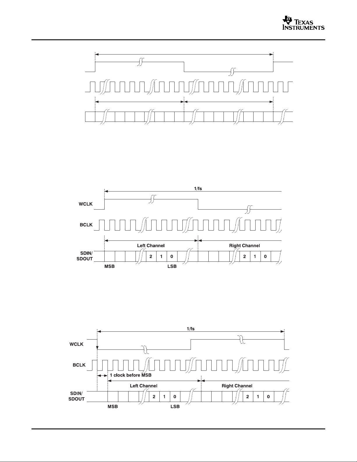
RIGHT JUSTIFIED MODE
In right-justified mode, the LSB of the left channel is valid on the rising edge of the bit clock preceding the falling
edge of word clock. Similarly, the LSB of the right channel is valid on the rising edge of the bit clock preceding
the rising edge of the word clock.
Submit Documentation Feedback
23
www.ti.com
BCLK
WCLK
SDIN/
SDOUT
n−2
1 00 1 0
1/fs
LSBMSB
LeftChannel RightChannel
n−3 2 2
n−1
n−2
n−3
n−1
n-1 n-2 n-3 n-1 n-2 n-3
n-1
n-3n-2
n-1 n-3n-2
TLV320AIC33
SLAS480A – JANUARY 2006 – REVISED JULY 2006
Figure 21. Right Justified Serial Bus Mode Operation
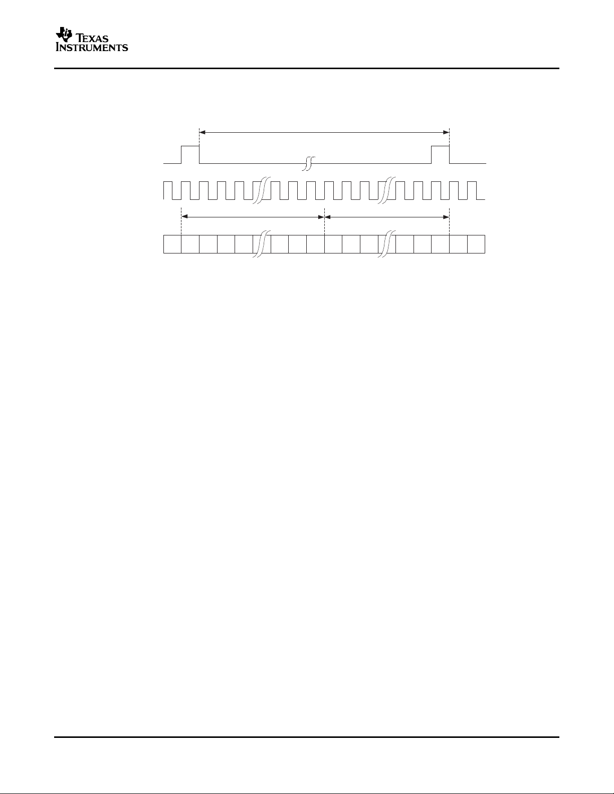
LEFT JUSTIFIED MODE
In left-justified mode, the MSB of the right channel is valid on the rising edge of the bit clock following the falling
edge of the word clock. Similarly the MSB of the left channel is valid on the rising edge of the bit clock following
the rising edge of the word clock.
Figure 22. Left Justified Serial Data Bus Mode Operation
I2S MODE
In I2S mode, the MSB of the left channel is valid on the second rising edge of the bit clock after the falling edge
of the word clock. Similarly the MSB of the right channel is valid on the second rising edge of the bit clock after
the rising edge of the word clock.
Figure 23. I2S Serial Data Bus Mode Operation
24
Submit Documentation Feedback
www.ti.com
BCLK
WCLK
SDIN/
SDOUT
n−2 n−3 1 0 n−1 n−2 1 0
1/fs
LSB
MSB
Left Channel Right Channel
n−1
MSB LSB
n−4 2 n−3 2
MSB
LSB
TLV320AIC33
SLAS480A – JANUARY 2006 – REVISED JULY 2006
DSP MODE
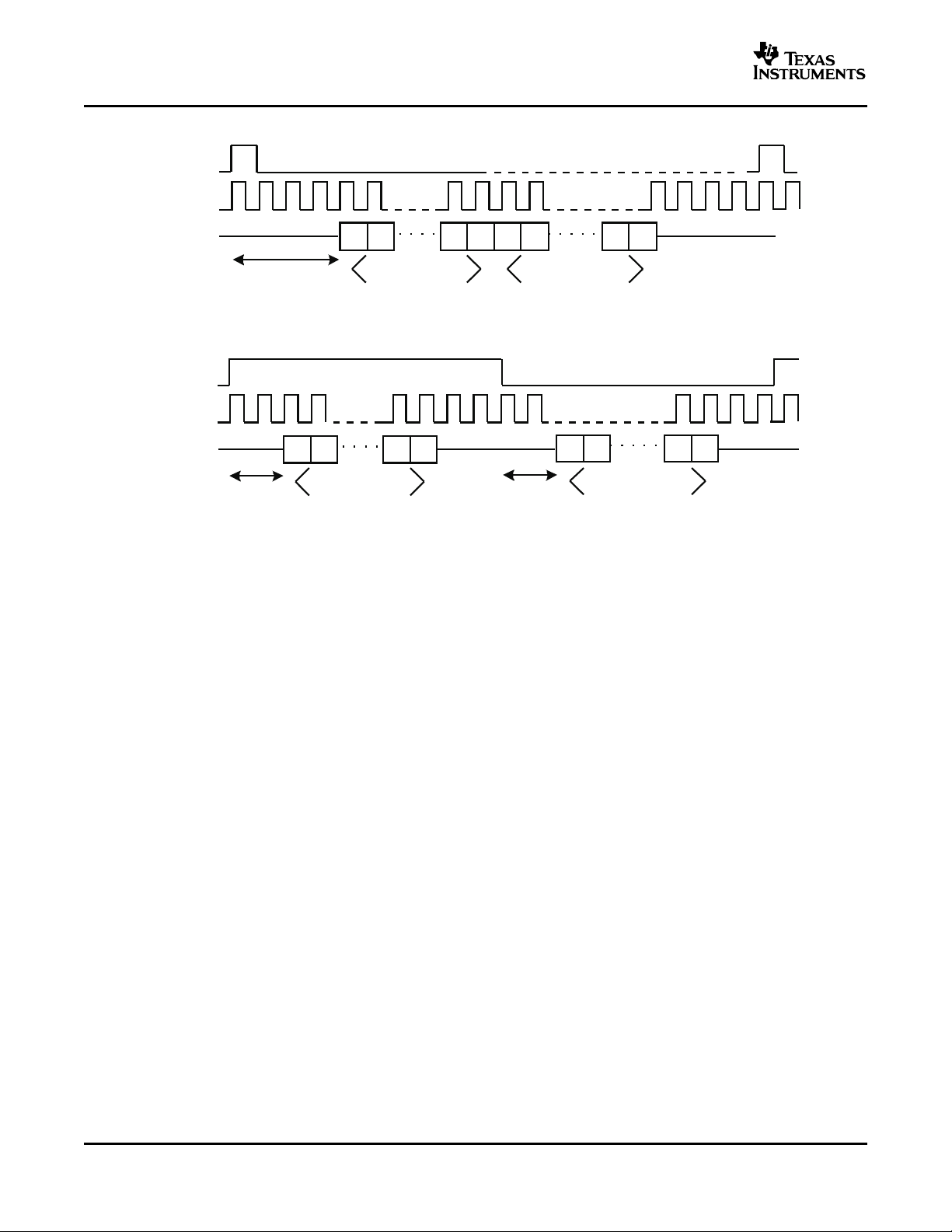
In DSP mode, the rising edge of the word clock starts the data transfer with the left channel data first and
immediately followed by the right channel data. Each data bit is valid on the falling edge of the bit clock.
Figure 24. DSP Serial Bus Mode Operation
TDM DATA TRANSFER
Time-division multiplexed data transfer can be realized in any of the above transfer modes if the 256-clock bit
clock mode is selected, although it is recommended to be used in either left-justified mode or DSP mode. By
changing the programmable offset, the bit clock in each frame where the data begins can be changed, and the
serial data output driver (DOUT) can also be programmed to tri-state during all bit clocks except when valid data
is being put onto the bus. This allows other codecs to be programmed with different offsets and to drive their
data onto the same DOUT line, just in a different slot. For incoming data, the codec simply ignores data on the
bus except where it is expected based on the programmed offset.
Note that the location of the data when an offset is programmed is different, depending on what transfer mode is
selected. In DSP mode, both left and right channels of data are transferred immediately adjacent to each other
in the frame. This differs from left-justified mode, where the left and right channel data will always be a
half-frame apart in each frame. In this case, as the offset is programmed from zero to some higher value, both
the left and right channel data move across the frame, but still stay a full half-frame apart from each other. This
is depicted in Figure 25 for the two cases.
Submit Documentation Feedback
25
www.ti.com
N-1 N-2 1 0 N-1 N-2 1 0
word
clock
bit clock
data
in/out
RightChannelData
RightChannelData
LeftChannelData
LeftChannelData
N-1 N-2 1 0 N-1 N-2 1 0
word
clock
bit clock
data
in/out
DSP Mode
LeftJustifiedMode
offset
offset
offset
TLV320AIC33
SLAS480A – JANUARY 2006 – REVISED JULY 2006
Figure 25. DSP Mode and Left Justified Modes, Showing the
Effect of a Programmed Data Word Offset
AUDIO DATA CONVERTERS
The TLV320AIC33 supports the following standard audio sampling rates: 8 kHz, 11.025 kHz, 12 kHz, 16 kHz,
22.05 kHz, 24 kHz, 32 kHz, 44.1 kHz, 48 kHz, 88.2 kHz, and 96 kHz. The converters can also operate at
different sampling rates in various combinations, which are described further below.
The data converters are based on the concept of an Fsref rate that is used internal to the part, and it is related
to the actual sampling rates of the converters through a series of ratios. For typical sampling rates, Fsref will be
either 44.1 kHz or 48 kHz, although it can realistically be set over a wider range of rates up to 53 kHz, with
additional restrictions applying if the PLL is used. This concept is used to set the sampling rates of the ADC and
DAC, and also to enable high quality playback of low sampling rate data, without high frequency audible noise
being generated.
The sampling rate of the ADC and DAC can be set to Fsref/NDAC or 2 × Fsref/NDAC, with NDAC being 1, 1.5, 2,
2.5, 3, 3.5, 4, 4.5, 5, 5.5, or 6.
While only one Fsref can be used at a time in the part, the ADC and DAC sampling rates can differ from each
other by using different NADC and NDAC divider ratios for each. For example, with Fsref=44.1-kHz, the DAC
sampling rate can be set to 44.1-kHz by using NDAC=1, while the ADC sampling rate can be set to 8.018-kHz
by using NADC=5.5.
When the ADCs and DACs are operating at different sampling rates, an additional word clock is required, to
provide information regarding where data begins for the ADC versus the DAC. In this case, the standard bit
clock signal (which can be supplied through the BCLK pin or through GPIO2) is used to transfer both ADC and
DAC data, the standard word clock signal is used to identify the start of the DAC data, and a separate ADC
word clock signal (denoted ADWK) is used. This clock can be supplied or generated from GPIO1 at the same
time the DAC word clock is supplied or generated from WCLK.
AUDIO CLOCK GENERATION
The audio converters in the TLV320AIC33 need an internal audio master clock at a frequency of 256 × Fsref,
which can be obtained in a variety of manners from an external clock signal applied to the device.
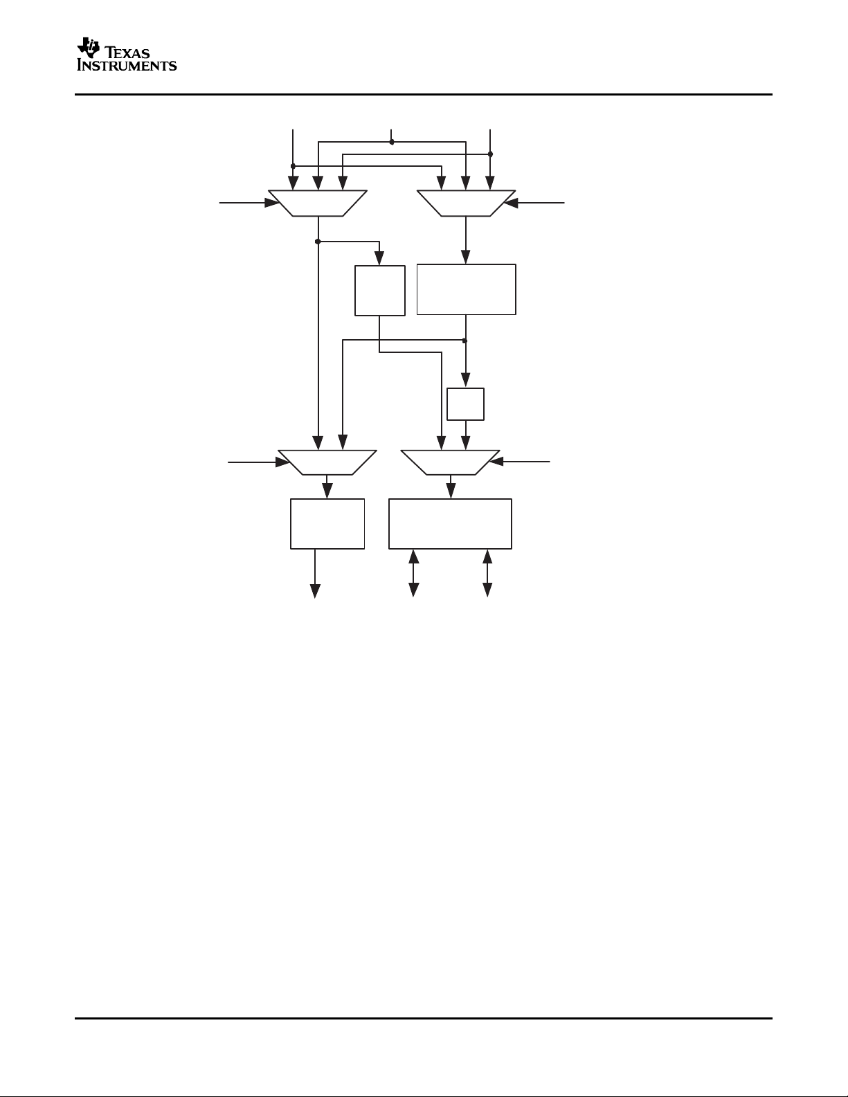
A more detailed diagram of the audio clock section of the TLV320AIC33 is shown in Figure 26 .
26
Submit Documentation Feedback
www.ti.com
2/Q
GPIO2
PLL_CLKIN
CODEC
CODEC_CLKIN
2/(N*M)
CLKMUX_OUT
GPIO1
PLL_OUT
K = J.D
J = 1,2,3,. . . , 62,63
D= 0000,0001, . . . ,9998,9999
R= 1,2,3,4, . . . ,15,16
P= 1,2, . . . . ,7,8
M =1,2,4,8
N = 2,3, . . . ., 16,17
MCLK BCLK
CLKDIV_IN
PLL_IN
WCLK= Fsref/ Ndac GPIO1= Fsref/ Nadc
ADC_FSDAC_FSCLKOUT
Ndac=1,1.5,2, . . ., 5.5,6
DAC DRA => Ndac = 0.5
ADC DRA => Nadc = 0.5
CODEC_CLK=256*Fsref
CLKOUT_IN
CLKDIV_OUT
1/8
PLLDIV_OUT
CLKDIV_CLKIN
Q = 3,3, . . . . ,16,17
K*R/P
Ndac=1,1.5,2, . . ., 5.5,6
TLV320AIC33
SLAS480A – JANUARY 2006 – REVISED JULY 2006
The part can accept an MCLK input from 512 kHz to 50 MHz, which can then be passed through either a
programmable divider or a PLL, to get the proper internal audio master clock needed by the part. The BCLK or
GPIO2 inputs can also be used to generate the internal audio master clock.
This design also allows the PLL to be used for an entirely separate purpose in a system, if the audio codec is
not powered up. The user can supply a separate clock to GPIO2, route this through the PLL, with the resulting
output clock driven out GPIO1, for use by other devices in the system
A primary concern is proper operation of the codec at various sample rates with the limited MCLK frequencies
available in the system. This device includes a highly programmable PLL to accommodate such situations
easily. The integrated PLL can generate audio clocks from a wide variety of possible MCLK inputs, with
particular focus paid to the standard MCLK rates already widely used.
When the PLL is disabled,
Where Q = 2, 3, … , 17
NOTE – when NDAC = 1.5, 2.5, 3.5, 4.5, or 5.5, odd values of Q are not allowed. In this mode, MCLK can be as
high as 50 MHz, and Fsref should fall within 39 kHz to 53 kHz.
When the PLL is enabled,
Figure 26. Audio Clock Generation Processing
Fsref = CLKDIV_IN / (128 × Q)
CLKDIV_IN can be MCLK, BCLK, or GPIO2, selected by register 102, bits D7-D6.
Submit Documentation Feedback
27

www.ti.com
TLV320AIC33
SLAS480A – JANUARY 2006 – REVISED JULY 2006
Fsref = (PLLCLK_IN × K × R) / (2048 × P), where
P = 1, 2, 3, … , 8
R = 1, 2, … , 16
K = J.D
J = 1, 2, 3, … , 63
D = 0000, 0001, 0002, 0003, … , 9998, 9999
PLLCLK_IN can be MCLK or BCLK, selected by Page 0, register 102, bits D5-D4
P, R, J, and D are register programmable. J is the integer portion of K (the numbers to the left of the decimal
point), while D is the fractional portion of K (the numbers to the right of the decimal point, assuming four digits of
precision).
Examples:
If K = 8.5, then J = 8, D = 5000
If K = 7.12, then J = 7, D = 1200
If K = 14.03, then J = 14, D = 0300
If K = 6.0004, then J = 6, D = 0004
When the PLL is enabled and D = 0000, the following conditions must be satisfied to meet specified
performance:
2 MHz ≤ ( PLLCLK_IN / P ) ≤ 20 MHz
80 MHz ≤ (PLLCLK _IN × K × R / P ) ≤ 110 MHz
4 ≤ J ≤ 55
When the PLL is enabled and D ≠ 0000, the following conditions must be satisfied to meet specified performance:
10 MHz ≤ PLLCLK _IN / P ≤ 20 MHz
80 MHz ≤ PLLCLK _IN × K × R / P ≤ 110 MHz
4 ≤ J ≤ 11
R = 1
Example:
MCLK = 12 MHz and Fsref = 44.1 kHz
Select P = 1, R = 1, K = 7.5264, which results in J = 7, D = 5264
Example:
MCLK = 12 MHz and Fsref = 48.0 kHz
Select P = 1, R = 1, K = 8.192, which results in J = 8, D = 1920
28
Submit Documentation Feedback
 Loading...