

Page 1
User's Guide
SLAU738–September 2017
TLV320AIC3109EVM-K
This user's guide describes the characteristics, operation, and use of the TLV320AIC3109EVM, both by
itself and as part of the TLV320AIC3109EVM-K. This evaluation module (EVM) is a complete mono audio
codec with several inputs and outputs, extensive audio routing, mixing, and effects capabilities. A
complete circuit description, schematic diagram, and bill of materials (BOM) are also included.
The following related documents are available through the Texas Instruments Web site at www.ti.com.
Table 1. EVM-Compatible Device Data Sheets
Device Literature Number
TLV320AIC3109-Q1 SLASE93
TPS73533-Q1 SBVS252
TAS1020B SLES025
Contents
1 EVM Overview ............................................................................................................... 3
2 EVM Description and Basics............................................................................................... 6
3 TLV320AIC3109EVM-K Setup and Installation ........................................................................ 12
4 TLV320AIC3109EVM Software........................................................................................... 13
Appendix A EVM Connector Descriptions .................................................................................... 33
Appendix B TLV320AIC3109EVM Schematic................................................................................ 37
Appendix C TLV320AIC3109EVM Layout Views ............................................................................ 40
Appendix D TLV320AIC3109EVM Bill of Materials.......................................................................... 43
Appendix E USB-MODEVM Schematic....................................................................................... 45
Appendix F USB-MODEVM Layout Views ................................................................................... 47
Appendix G USB-MODEVM Bill of Materials................................................................................. 49
Appendix H TLV320AIC3109-Q1 Configuration Scripts .................................................................... 51
Appendix I USB-MODEVM Protocol ......................................................................................... 56
List of Figures
1 TLV320AIC3109EVM Block Diagram .................................................................................... 3
2 TLV320AIC3109EVM Board ............................................................................................... 4
3 USB-MODEVM Board....................................................................................................... 5
4 Analog Section of the TLV320AIC3109EVM............................................................................. 9
5 Digital Section of the TLV320AIC3109EVM ............................................................................ 10
6 Power Supplies for Stand-Alone Operation............................................................................. 11
7 Device Selection Window................................................................................................. 14
8 Default Software Screen .................................................................................................. 14
9 Audio Input and ADC Tab ................................................................................................ 16
10 Bypass Paths ............................................................................................................... 17
11 Audio Interface Tab ....................................................................................................... 18
12 Clocks Tab ................................................................................................................. 19
Microsoft, Windows are registered trademarks of Microsoft Corporation.
SPI is a trademark of Motorola, Inc.
VISA, LabVIEW are trademarks of National Instruments Corporation.
All other trademarks are the property of their respective owners.
SLAU738–September 2017
Submit Documentation Feedback
Copyright © 2017, Texas Instruments Incorporated
TLV320AIC3109EVM-K
1
Page 2

www.ti.com
13 AGC Tab .................................................................................................................... 21
14 Advanced AGC settings................................................................................................... 21
15 Filters Tab .................................................................................................................. 22
16 ADC High Pass Filters .................................................................................................... 23
17 DAC Filters.................................................................................................................. 23
18 De-emphasis Filters........................................................................................................ 24
19 Shelf Filters ................................................................................................................. 25
20 EQ Filters ................................................................................................................... 25
21 Analog Simulation Filters ................................................................................................. 26
22 Preset Filters ............................................................................................................... 26
23 User Filters ................................................................................................................. 26
24 3D Effect Settings ......................................................................................................... 27
25 Output Stage Configuration Tab ......................................................................................... 27
26 DAC/Line Outputs Tab .................................................................................................... 29
27 High-Power Outputs Tab ................................................................................................. 30
28 Command Line Interface Tab ............................................................................................ 31
29 File Menu ................................................................................................................... 32
30 TLV320AIC3109-Q1 Main Schematics.................................................................................. 37
31 Connector, Test Points, and Power Distribution Schematics......................................................... 38
32 TLV320AIC3109EVM Hardware ......................................................................................... 39
33 TLV320AIC3109EVM Assembly Layer.................................................................................. 40
34 TLV320AIC3109EVM Top Layer......................................................................................... 40
35 TLV320AIC3109EVM Ground Layer..................................................................................... 41
36 TLV320AIC3109EVM Power Layer...................................................................................... 41
37 TLV320AIC3109EVM Bottom Layer..................................................................................... 42
38 TLV320AIC3109EVM Bottom Assembly Layer ........................................................................ 42
39 USB-MODEVM Interface Board Schematic (1 of 2)................................................................... 45
40 USB-MODEVM Interface Board Schematic (2 of 2)................................................................... 46
41 USB-MODEVM Assembly Layer......................................................................................... 47
42 USB-MODEVM Top Layer................................................................................................ 48
43 USB-MODEVM Bottom Layer ............................................................................................ 48
List of Tables
1 EVM-Compatible Device Data Sheets .................................................................................... 1
2 List of Jumpers............................................................................................................... 6
3 USB-MODEVM SW2 Settings ............................................................................................. 7
4 USB-MODEVM Jumpers ................................................................................................... 7
5 TLV320AIC3109EVM and TLV320AIC3104 GUI Signal Name Relation .......................................... 13
6 Analog Interface Pinout.................................................................................................... 33
7 Alternate Analog Connectors............................................................................................. 34
8 Digital Interface Pinout .................................................................................................... 35
9 Power Supply Pinout....................................................................................................... 36
10 TLV320AIC3109EVM Bill of Materials................................................................................... 43
11 USB-MODEVM Bill of Materials.......................................................................................... 49
12 USB Control Endpoint HIDSETREPORT Request .................................................................... 56
13 Data Packet Configuration................................................................................................ 56
14 GPIO Pin Assignments .................................................................................................... 59
2
TLV320AIC3109EVM-K
Copyright © 2017, Texas Instruments Incorporated
SLAU738–September 2017
Submit Documentation Feedback
Page 3
EVM Position 1
External Power
Supply Input
USB
Input
External
Control Input
External Digital
Audio Input
TAS1020B
Controller
EVM Position 2
USB-MODEVM Motherboard
TLV320AIC3109Q1EVM
TLV320AIC3109-Q1
I²C, SPI I²S
Copyright © 2017, Texas Instruments Incorporated
www.ti.com
1 EVM Overview
1.1 Features
This EVM supports the following features:
• Complete development kit for the evaluation of the TLV320AIC3109-Q1 mono audio codec.
• Connection points are available for line inputs and outputs, external microphone, and mono
headphone.
• Onboard microphone for ADC evaluation.
• Direct access to digital audio signals and control interface is provided for simple system integration.
• USB connection to PC provides power, control, and streaming audio data for easy evaluation.
1.2 Introduction
The TLV320AIC3109EVM-K is a complete evaluation and demonstration kit, which includes the
TLV320AIC3109EVM and a USB-based motherboard called the USB-MODEVM Interface board. The
TLV320AIC3109EVM-K is operational with one USB cable connection to a personal computer. The USB
connection provides power, control, and streaming audio data to the EVM kit for reduced setup and
configuration. The EVM kit also provides connection points for control signals, audio data, and power for
advanced operation, which allows prototyping and connection to the end-user system evaluation. The
TLV320AIC3109EVM-K is controlled and configured with the TLV320AIC310xEVM-K Graphical User
Interface (GUI) Software, compatible with Microsoft®Windows®operating systems.
EVM Overview
1.2.1 TLV320AIC3109EVM-K Block Diagram
The TLV320AIC3109EVM consists of two separate circuit boards, the USB-MODEVM and the
TLV320AIC3109EVM. The USB-MODEVM is built around a TAS1020B streaming audio USB controller
with an 8051-based core.
The USB-MODEVM has two EVM positions that allow for the connection of two small evaluation modules
or one larger evaluation module. The TLV320AIC3109EVM is designed to fit over both of the smaller
evaluation module slots as shown in Figure 1.
SLAU738–September 2017
Submit Documentation Feedback
Figure 1. TLV320AIC3109EVM Block Diagram
Copyright © 2017, Texas Instruments Incorporated
TLV320AIC3109EVM-K
3
Page 4
PREVIEW ONLY
EVM Overview
1.2.1.1 TLV320AIC3109EVM
The TLV320AIC3109EVM showcases the latest Texas Instruments (TI) mono audio codec, the
TLV320AIC3109-Q1 (U3). The TLV320AIC3109-Q1 device is a low-power mono audio codec with a mono
headphone amplifier and multiple input and output channels that are programmable in single-ended or
fully differential configurations.
The EVM offers different test points, terminals and headers used to evaluate, test and configure the
TLV320AIC3109 audio codec in the board. The layout of the board separates analog and digital sections
all layers; the analog input and outputs, and analog power supply regulator are located in the left side of
the board, while the right side of the board has all the digital signals, like the I²C lines, digital audio signals
and onboard EEPROM. Ground planes for both analog and digital grounds are separated, but two
common connection points are available through headers J28 and J29. The EVM was designed following
the layout recommendations from TLV320AIC3109-Q1 Automotive, Low-Power, 96-kHz, Mono Audio
Codec. Several connectors at the edge of the board provide access to the different inputs and outputs of
the device. Options to evaluate special features, such as capless headphone configuration and internal
mic bias generation are also available. Power, digital audio data, and digital connection for the
configuration and control of the device is provided by the USB-MODEVM board. The Figure 2 shows the
TLV320AIC3109EVM board.
www.ti.com
Figure 2. TLV320AIC3109EVM Board
4
TLV320AIC3109EVM-K
Copyright © 2017, Texas Instruments Incorporated
SLAU738–September 2017
Submit Documentation Feedback
Page 5
www.ti.com
1.2.1.2 USB-MODEVM Interface Board
The USB-MODEVM board is a motherboard used to configure, control, and provide an interface between
a computer and evaluation modules with TI modular EVM form factor. The simple diagram shown in
Figure 1 shows only the basic features of the USB-MODEVM Interface board. The USB-MODEVM
Interface board is intended to be used in USB mode, where control of the installed EVM is accomplished
using the onboard USB controller device, the TAS1020B. Provision is made, however, for driving all the
data buses (I2C, SPI™, I2S/AC97) externally. The source of these signals is controlled by SW2 on the
USB-MODEVM. Refer to Table 3 for details on the switch settings.
Because the TLV320AIC3109EVM is a double-wide modular EVM, it is installed with connections to both
EVM positions, which connects the TLV320AIC3109-Q1 digital interface to the I2C control port and audio
interface of the TAS1020B.
In the factory configuration, the board is ready to use with the TLV320AIC3109EVM. To view all the
functions and configuration options available on the USB-MODEVM board, see the USB-MODEVM
Interface Board schematic in Appendix E.
EVM Overview
SLAU738–September 2017
Submit Documentation Feedback
Figure 3. USB-MODEVM Board
Copyright © 2017, Texas Instruments Incorporated
TLV320AIC3109EVM-K
5
Page 6

EVM Description and Basics
2 EVM Description and Basics
This section provides information on the analog input and output, digital control, power and general
connection of the TLV320AIC3109EVM-K.
2.1 Default Configuration and Connections
2.1.1 TLV320AIC3109EVM Default Connections
Table 2 provides a list of jumpers found on the EVM and their factory default conditions.
Table 2. List of Jumpers
www.ti.com
Jumper Default
Position
J7 2-3 Mic bias selection: when connecting 2-3, mic bias comes from the MICBIAS pin
on the device; when connecting 1-2, mic bias is supplied from an external power
source connected to J6
J8 Open Connects onboard Mic to IN1P
J11 Open When installed, shorts across the input AC coupling capacitor on IN2M, for DC
measuring purposes only
J12 Open When installed, shorts across the input AC coupling capacitor on IN2P, for DC
measuring purposes only
J14 Open When installed, shorts across the input AC coupling capacitor on IN1M, for DC
measuring purposes only
J15 Open When installed, shorts across the input AC coupling capacitor on IN1P, for DC
measuring purposes only
J18 Open When installed, shorts across the output capacitor on HPCOM; remove this
jumper if using AC-coupled output drive
J19 Open When installed, shorts across the output capacitor on HPOUT; remove this
jumper if using AC-coupled output drive
J22 2-3 IOVDD selection: when connecting 2-3, IOVDD is set to +3.3 VD; when
connecting 1-2, IOVDD and DVDD are shorted at +1.8 VD
J23 Open When installed, allows the USB-MODEVM to hardware reset the device under
user control
J24 Installed Provides a measuring point for AVDD current
J25 Installed Provides a measuring point for DRVDD current
J26 Installed Provides a measuring point for DVDD current
J27 Installed Provides a measuring point for IOVDD current
J28 Installed Connects analog and digital grounds on the lower part the board
J29 Installed Connects analog and digital grounds on the upper part the board
J30 Open Selects onboard EEPROM as firmware source
Jumper Description
6
TLV320AIC3109EVM-K
Copyright © 2017, Texas Instruments Incorporated
SLAU738–September 2017
Submit Documentation Feedback
Page 7
www.ti.com
2.1.2 USB-MODEVM Default Setting
Table 3 provides a list of the SW2 settings on the USB=MODEVM. For use with the TLV320AIC3109EVM,
set SW-2 positions 1 through 7 to ON, and set SW-2.8 to OFF.
Table 3. USB-MODEVM SW2 Settings
EVM Description and Basics
SW-2 Switch
Number
1 A0 USB-MODEVM EEPROM I2C Address A0
2 A1 USB-MODEVM EEPROM I2C Address A1
3 A2 USB-MODEVM EEPROM I2C Address A2
4 USB I2S I2S Bus Source Selection
5 USB MCK I2S Bus MCLK Source Selection
6 USB SPI SPI Bus Source Selection
7 USB RST RST Source Selection
8 EXT MCK External MCLK Selection
Label Switch Description
ON: A0 = 0
OFF: A0 = 1
ON: A1 = 0
OFF: A1 = 1
ON: A2 = 0
OFF: A2 = 1
ON: I2S Bus connects to TAS1020
OFF: I2S Bus connects to USB-MODEVM J14
ON: MCLK connects to TAS1020
OFF: MCLK connects to USB-MODEVM J14
ON: SPI Bus connects to TAS1020
OFF: SPI Bus connects to USB-MODEVM J15
ON: EVM Reset Signal comes from TAS1020
OFF: EVM Reset Signal comes from USB-MODEVM J15
ON: MCLK Signal is provided from USB-MODEVM J10
OFF: MCLK Signal comes from either selection of SW2-5
Table 4 provides a list of USB-MODEVM jumpers found on the EVM.
Table 4. USB-MODEVM Jumpers
Jumper Default Position Jumper Description
JMP1 Installed Connects analog and digital +5-V supplies
JMP2 Open Connects analog and digital grounds
JMP3 Open Connects I2C SDA pullup to IOVDD
JMP4 Open Connects I2C SCL pullup to IOVDD
JMP5 2-3 When connecting 2-3, SS comes from FSX; when connecting 1-2, SS
JMP6 1-2 When connecting 1-2, +5 VD comes from USB; when connecting 2-3, +5
JMP7 1-2 When connecting 1-2, MCLKI comes from USB; when connecting 2-3,
JMP8 Open Connects resistor across EXT MCLK
comes from CNTL
VD comes from U2
MCLKI comes from AVSS and DVSS
SLAU738–September 2017
Submit Documentation Feedback
Copyright © 2017, Texas Instruments Incorporated
TLV320AIC3109EVM-K
7
Page 8

EVM Description and Basics
2.2 Analog Signals
2.2.1 Analog Inputs
The analog inputs to the EVM can be connected through two different methods. The analog input sources
can be applied directly to J1 (top or bottom side) or through the analog headers (J10, J13, and J9) around
the edge of the board. The connection details of each header and connector are found in Appendix A.
The TLV320AIC3109EVM provides a header in parallel with the input capacitors of each one of the IN1
and IN2 inputs; these headers are provided so end-user can configure the device for DC measurement.
Refer to TLV320AIC3109-Q1 Automotive, Low-Power, 96-kHz, Mono Audio Codec for details on the line
input specifications.
In addition to the IN1 and IN2 line input connectors, the EVM features an onboard microphone and a
mono jack for an external microphone, both connected to IN1P input. When the onboard microphone is
used, header J8 must be shorted and J9 should not be connected. Similarly, when external mic is used,
J8 should be disconnected. Both microphones are biased to the MICBIASIN bias signal, that can be
selected with header J7 from either internal mic bias of the audio codec or an external source connected
to J6. Details about the location of the analog inputs of the TLV320AIC3109EVM are shown in Figure 4.
2.2.2 Analog Output
The analog outputs to the EVM can be connected through two different methods. The analog outputs are
available from the J1 and J2 (top or bottom) or they may be accessed through J16, J17, J20, and J21 at
the edges of the board. The connection details can be found in Appendix A.
The line outputs of the TLV320AIC3109-Q1 include the recommended low pass filter to remove the out-ofband noise that can affect the performance of the receiver device. The headphone output of the EVM
includes a low pas filter used for test equipment measurement, available in HPCOM_LPF and
HPOUT_LPF test points. Headers J18 and J19 are used to bypass the AC-coupling capacitors of the
headphone output so the headphone output terminal can be used in Capless mode. In addition to the
headphone output terminal, a mono jack connector (J16) is included to connect a mono headphone with a
typical 3.5mm connector. This jack can be configured to support either AC-Couple or Capless mode by
changing the position of switch SW1. The selection on the headphone output mode should match with the
configuration of the audio codec. Refer to section Section 4.9 for more details on the headphone output
mode configuration. The analog output section of the EVM is shown in Figure 4.
www.ti.com
8
TLV320AIC3109EVM-K
Copyright © 2017, Texas Instruments Incorporated
SLAU738–September 2017
Submit Documentation Feedback
Page 9
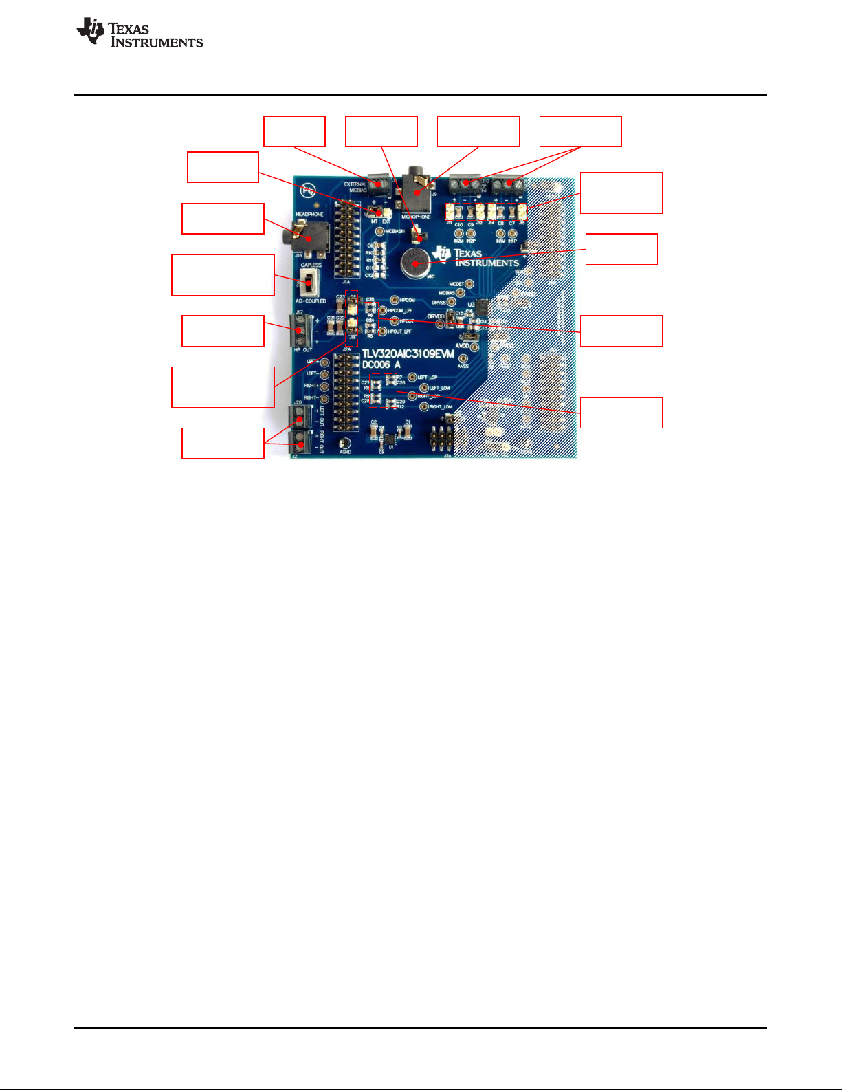
IN1 and IN2 Input
Terminals
External Microphone
3.5-mm Jack
External
Micbias
Terminal
Headers to Bypass
AC-Coupling caps
for IN1 and IN2
Onboard
Microphone
Switch to set
CAPLESS or AC-Coupled
Headphone Jack Output
Mono Headphone
3.5-mm Jack
Mono Headphone
Output Terminal
Headers to set
CAPLESS or AC-Coupled
HP Output Terminal
Left and Right Line
Output Terminals
Out-of-Band Noise
Low Pass Filter
Low-Pass Filter for
Measuring HP
Output
Micbias Selection
Header
Onboard Mic
Header to IN1
www.ti.com
EVM Description and Basics
Figure 4. Analog Section of the TLV320AIC3109EVM
SLAU738–September 2017
Submit Documentation Feedback
Copyright © 2017, Texas Instruments Incorporated
TLV320AIC3109EVM-K
9
Page 10
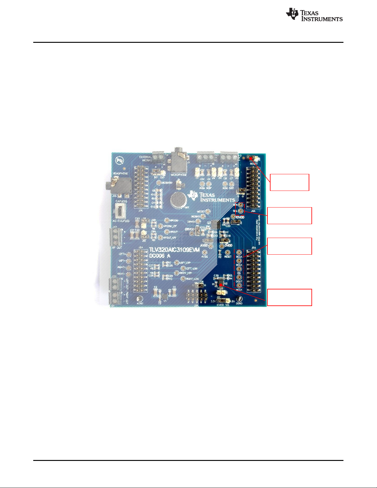
+HDGHUIRU*8,¶V
Hardware Reset
Onboard EEPROM
Test Points for Digital
Audio Signals
Test Points for
I²C Signals
EVM Description and Basics
2.3 Digital Signals
2.3.1 Digital Inputs and Outputs
The digital inputs and outputs of the EVM can be monitored through J4 and J5. If external signals need to
be connected to the EVM, digital inputs should be connected via J14 and J15 on the USB-MODEVM and
the SW2 in the motherboard switch should be changed accordingly (see Section 2.1.2). The connector
details are available in Section A.2.
The EVM features test points to directly measure the digital audio signals coming from the USB-MODEVM
board. Additionally, test points are provided to monitor the I²C control signals. A header to connect the
RESET pin of the codec with hardware reset signal from the motherboard is provided. This is useful so the
user can perform a hardware reset for the audio codec from the GUI without any board modification. The
digital section of the TLV320AIC3109EVM is shown in Figure 5.
www.ti.com
2.4 Power Connections
The TLV320AIC3109EVM requires three power supplies to fully evaluate the audio codec:
• +5-V power supply, required to generate +3.3-V supply from the integrated low-dropout voltage
regulator (U1) to feed analog power supplies of the codec (AVDD and DRVDD).
• +1.8-V power supply, required to feed the digital core voltage supply (DVDD) and digital input and
output voltage supply (IOVDD) of the codec. The selection for the digital input and output voltage
(IOVDD) is made via IOVDD SEL header (J22).
• +3.3-V power supply, required for digital input and output voltage supply (IOVDD) of the codec.
The EVM can be powered by external power supplies when being used in stand-alone operation or by the
USB-MODEVM when it is plugged onto the motherboard. The following sections discuss each operation
mode.
10
TLV320AIC3109EVM-K
Figure 5. Digital Section of the TLV320AIC3109EVM
Copyright © 2017, Texas Instruments Incorporated
SLAU738–September 2017
Submit Documentation Feedback
Page 11
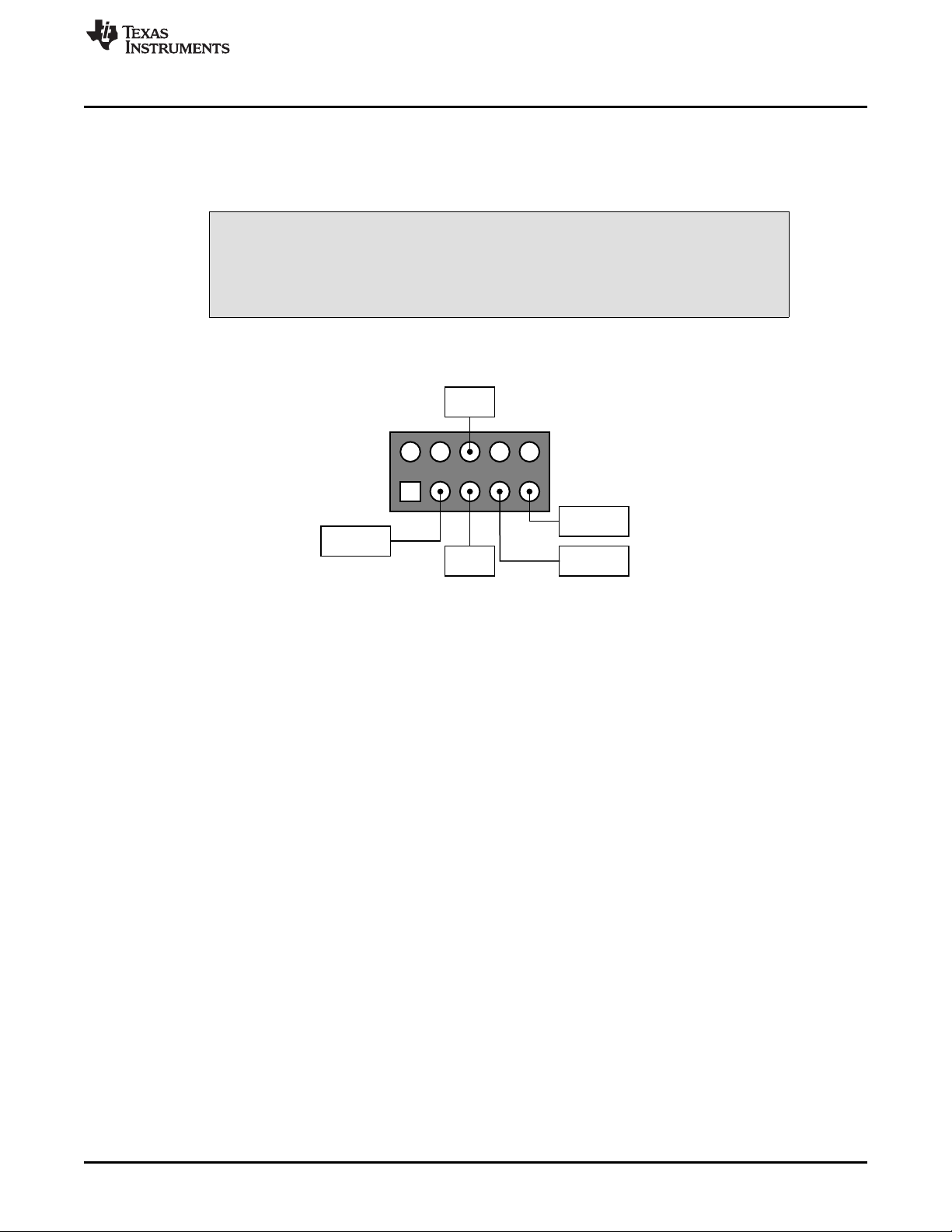
+5-V Analog
Supply
+1.8-V Digital
Supply
+3.3-V Digital
Supply
Analog
Ground
Digital
Ground
J3
www.ti.com
2.4.1 Stand-Alone Operation
When used as a stand-alone EVM, power is applied to J3 directly, making sure to reference the supplies
to the appropriate grounds on that connector. The diagram for the power supplies required for stand-alone
operation mode are shown in Figure 6.
Verify that all power supplies are within the safe operating limits shown in
TLV320AIC3109-Q1 Automotive, Low-Power, 96-kHz, Mono Audio Codec
before applying power to the EVM.
J3 provides connection to the common power bus for the TLV320AIC3109EVM. Power is supplied on the
pins listed in Table 9.
EVM Description and Basics
CAUTION
Figure 6. Power Supplies for Stand-Alone Operation
2.4.2 USB-MODEVM Operation
The USB-MODEVM Interface board can be powered from several different sources:
• USB
• 6-Vdc to 10-Vdc AC/DC external wall supply (not included)
• Lab power supply
When powered from the USB connection, JMP6 should have a shunt from pins 1–2 (this is the default
factory configuration). When powered from 6-V to 10-Vdc, either through the J8 terminal block or J9 barrel
jack, JMP6 should have a shunt installed on pins 2–3. If power is applied in any of these ways, onboard
regulators generate the required supply voltages and no further power supplies are necessary.
If laboratory supplies are used to provide the individual voltages required by the USB-MODEVM Interface,
JMP6 should have no shunt installed. Voltages are then applied to J2 (+5 VA), J3 (+5 VD), J4 (+1.8 VD),
and J5 (+3.3 VD). The +1.8 VD and +3.3 VD can also be generated on the board by the onboard
regulators from the +5 VD supply; to enable this configuration, the switches on SW1 need to be set to
enable the regulators by placing them in the ON position (lower position, looking at the board with text
reading right-side up). If +1.8 VD and +3.3 VD are supplied externally, disable the onboard regulators by
placing SW1 switches in the OFF position.
Each power supply voltage has an LED (D1–D7) that lights when the power supplies are active.
SLAU738–September 2017
Submit Documentation Feedback
Copyright © 2017, Texas Instruments Incorporated
TLV320AIC3109EVM-K
11
Page 12

TLV320AIC3109EVM-K Setup and Installation
3 TLV320AIC3109EVM-K Setup and Installation
The following section provides information on using the TLV320AIC3109EVM-K, including set up, program
installation, and program usage.
NOTE: If using the EVM in stand-alone mode, the software should be installed per Section 3.1, but
the hardware configuration may be different.
3.1 Software Installation
1. Download the latest version of the TLV320AIC310xEVM-K GUI.
2. Unzip the installation file by clicking on the self-extracting zip file.
3. Install the EVM software by double-clicking the Setup executable and follow the directions. The user
may be prompted to restart their computer.
4. Install the most up-to-date version of National Instrument’s VISA™ drivers.
5. For Windows 7 and above operating systems, download and install the USB-MODEVM Windows
XP/Vista/7 Drivers.
3.2 EVM Connections
1. Ensure that the TLV320AIC3109EVM is installed on the USB-MODEVM Interface board, aligning J1,
J2, J3, J4, and J5 with the corresponding connectors on the USB-MODEVM.
2. Verify that the jumpers and switches are in their default conditions.
3. Attach a USB cable from the PC to the USB-MODEVM Interface board. The default configuration will
provide power, control signals, and streaming audio via the USB interface from the PC. On the USBMODEVM, LEDs D3–5 and D7 should light to indicate the power is being supplied from the USB.
4. For the first connection, the PC should recognize new hardware and begin an initialization process.
The user may be prompted to identify the location of the drivers or allow the PC to automatically
search for them. Allow the automatic detection option.
5. Once the PC confirms that the hardware is operational, D2 on the USB-MODEVM should light to
indicate that the firmware has been loaded and the EVM is ready for use. If the LED is not lit, verify
that the drivers were installed by trying to unplug and restart at Step 3. If further problems are found,
please refer to the TLV320AIC3xEVM-PDK Series Troubleshooting Guide.
After the TLV320AIC3109EVM software installation is complete, evaluation and development with the
TLV320AIC3109EVM-K can begin.
www.ti.com
12
TLV320AIC3109EVM-K
Copyright © 2017, Texas Instruments Incorporated
SLAU738–September 2017
Submit Documentation Feedback
Page 13

www.ti.com
4 TLV320AIC3109EVM Software
The TLV320AIC3109-Q1 audio codec is a mono version of the TLV320AIC3104 device, so the
configuration and control of the TLV320AIC3109EVM is made using the TLV320AIC3104EVM software.
Some features of the TLV320AIC3104EVM GUI will not be available for the TLV320AIC3109EVM,
detailed information about these features are included in the following sections. As the GUI is adapted for
the TLV320AIC3104 device, the names for the signal and internal channels are not the same in some
cases for the TLV320AIC3109. In general, the single channel of the TLV320AIC3109-Q1 corresponds to
the left channel of the TLV320AIC3104, being the only exception the single headphone output, that
corresponds to the right headphone output of the TLV320AIC3104. Table 5 indicates the relationship
between the GUI and TLV320AIC3109-Q1 signal and internal block names.
Table 5. TLV320AIC3109EVM and TLV320AIC3104 GUI
TLV320AIC3104 GUI TLV320AIC3109EVM
Right ADC not used
Right DAC not used
Right AGC not used
IN1L/LINE1L IN1/LINE1
IN1R/LINE1R IN2/LINE2
IN2L/LINE2L not used
IN2R/LINE2R not used
HPRCOM HPCOM
TLV320AIC3109EVM Software
Signal Name Relation
Name
Left ADC ADC
Left DAC DAC
Left AGC AGC
HPROUT HPOUT
HPLCOM not used
HPLOUT not used
TI recommends using only the features mentioned in this user's guide for the evaluation of the
TLV320AIC3109-Q1 audio codec; otherwise, the device could present unexpected behavior.
The following section discusses the details and operation of the EVM software.
NOTE: For codec configuration, the TLV320AIC3109-Q1 block diagram located in TLV320AIC3109-
Q1 Automotive, Low-Power, 96-kHz, Mono Audio Codec is a good reference to help
determine the signal routing.
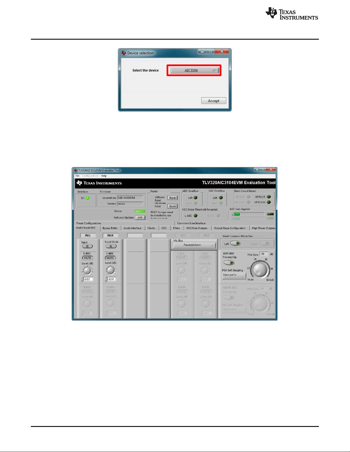
4.1 Device Selection for Operation With TLV320AIC3109EVM
The software that is installed provides operation for several devices of the TLV320AIC310X family of
audio codecs. An initial window should appear that looks like Figure 7. For operation with the
TLV320AIC3109EVM, the user should select AIC3104 from the pull-down menu and click Accept. The
program will take a few seconds to configure the software for operation before proceeding. A progress bar
should appear and show the status of the configuration.
SLAU738–September 2017
Submit Documentation Feedback
Copyright © 2017, Texas Instruments Incorporated
TLV320AIC3109EVM-K
13
Page 14
TLV320AIC3109EVM Software
Once the device is properly configured, the main window of the TV320AIC310x GUI appears. Figure 8
shows the default screen of the GUI. The sections that are shaded in the following captures of the
TLV320AIC3104 GUI are not available for the TLV320AIC3109-Q1 evaluation. TI recommends not
changing any of the parameters in these sections, otherwise, the performance and behavior of the device
cannot be assured.
www.ti.com
Figure 7. Device Selection Window
14
TLV320AIC3109EVM-K
Figure 8. Default Software Screen
Copyright © 2017, Texas Instruments Incorporated
SLAU738–September 2017
Submit Documentation Feedback
Page 15

www.ti.com
4.2 Front Page Indicators and Functions
Figure 8 illustrates the main screen of the EVM software. The indicators and buttons located above the
tabbed section of the front page are visible regardless of which tab is currently being selected.
NOTE: All the indicators corresponding to unused blocks of the TLV320AIC3109-Q1 should be
ignored. Refer to Table 5 for more information about the unused sections.
At the top left of the screen is an Interface indicator. This indicator shows which interface is selected for
controlling the TLV320AIC3109-Q1, only I2C is available for this device.
To the right of the Interface indicator is a group box called Firmware. This box indicates where the
firmware being used is operating from – in this release, the firmware is on the USB-MODEVM, so the user
should see USB-MODEVM in the box labeled Located On:. The version of the firmware appears in the
Version box below the Located On: box.
To the right, the next group box contains controls for resetting the TLV320AIC3109-Q1. A software reset
can be done by writing to a register in the TLV320AIC3109-Q1, and this is accomplished by pushing the
button labeled Software Reset. The TLV320AIC3109-Q1 also may be reset by toggling a pin on the
TLV320AIC3109-Q1, which is done by pushing the Hardware Reset button.
In order to perform a hardware reset, the RESET jumper (JMP19) must be
installed and SW2–7 on the USB-MODEVM must be turned OFF. Failure to do
either of these steps results in not generating a hardware reset or causing
unstable operation of the EVM, which may require cycling power to the USBMODEVM.
TLV320AIC3109EVM Software
CAUTION
Below the Firmware box, the Device Connected LED should be green when the EVM is connected. If the
indicator is red, the EVM is not properly connected to the PC. Disconnect the EVM and verify that the
drivers were correctly installed, then reconnect; if it does not work, try restarting the software.
On the upper right portion of the screen, several indicators are located which provide the status of various
portions of the TLV320AIC3109-Q1. These indicators are activated by pressing the Indicator Updates
button below the Device Connected LED. These indicators, as well as the other indicators on this panel,
are updated only when the front panel of the software is inactive, once every 20 ms.
The ADC Overflow and DAC Overflow indicators light when the overflow flags are set in the
TLV320AIC3109-Q1. Below these indicators are the AGC Noise Threshold Exceeded indicators that
show when the AGC noise threshold is exceeded. To the far right of the screen, the Short Circuit Detect
indicators show when a short-circuit condition is detected, if this feature has been enabled. Below the
short-circuit indicators, the AGC Gain Applied indicators use a bar graph to show the amount of gain
which has been applied by the AGC, and indicators that light when the AGC is saturated.
SLAU738–September 2017
Submit Documentation Feedback
Copyright © 2017, Texas Instruments Incorporated
TLV320AIC3109EVM-K
15
Page 16
TLV320AIC3109EVM Software
4.3 Audio Input/ADC Tab
The Audio Input/ADC tab allows control of the analog input mixer and the ADC. The controls are
displayed to look similar to an audio mixing console, as shown in Figure 9. Each analog input channel has
a vertical strip that corresponds to that channel. By default, all inputs are muted when the
TLV320AIC3109EVM is powered up.
www.ti.com
Figure 9. Audio Input and ADC Tab
To route an analog input to the ADC:
1. Select the Input Mode button to correctly show if the input signal is single-ended (SE) or fullydifferential (Diff). Inputs that are single-ended should be made to the positive signal terminal.
2. Click on the button of the analog input channel that corresponds to the correct ADC. The caption of the
button should change to Active.
3. Adjust the Level control to the desired attenuation for the connected channel. This level adjustment
can be done independently for each connection.
The TLV320AIC3109-Q1 offers a programmable microphone bias that can either be powered down or set
to 2 V, 2.5 V, or the power supply voltage of the ADC (AVDD_ADC). Control of the microphone bias (mic
bias) voltage is accomplished by using the Mic Bias pull-down menu button above the last two channel
strips. To use the onboard microphone, J8 must be installed and nothing should be plugged into J9. In
order for the mic bias settings in the software to take effect, J7 should be set to connect positions 2 and 3
(INT), so that mic bias is controlled by the TLV320AIC3109-Q1.
In the upper right portion of this tab are controls for Weak Common Mode Bias. Enabling these controls
will result in unselected inputs to the ADC to be weakly biased to the ADC common mode voltage.
Below these controls are the controls for the ADC PGA, including the master volume controls for the ADC
inputs. The ADC channel can be powered up or down as needed using the Powered Up button. PGA
soft-stepping for the ADC channel is selected using the pull-down menu control. The large knob sets the
actual ADC PGA Gain and allows adjustment of the PGA gains from 0 dB to 59.5 dB, in 0.5-dB steps
(excluding Mute). At the extreme counterclockwise rotation, the channel is muted. Rotating the knob
clockwise increases the PGA gain, which is displayed in the box directly above the volume control.
16
TLV320AIC3109EVM-K
Copyright © 2017, Texas Instruments Incorporated
SLAU738–September 2017
Submit Documentation Feedback
Page 17
www.ti.com
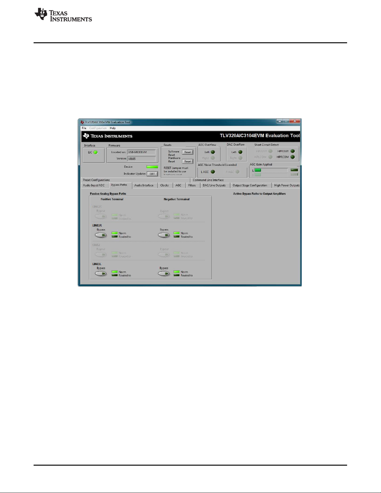
4.4 Bypass Paths
The Bypass Paths tab shows the active and passive bypass paths available for control.
The passive analog bypass paths allow the inputs to be routed straight through the device to the outputs
without turning on any of the internal circuitry. This provides a signal path through the device with minimal
power consumption.
The active bypass paths allow the inputs to bypass the ADC and DAC functional blocks and be routed to
the analog output mixers to be summed into the output amplifiers. The Bypass Paths tab is shown in
Figure 10.
TLV320AIC3109EVM Software
SLAU738–September 2017
Submit Documentation Feedback
Figure 10. Bypass Paths
Copyright © 2017, Texas Instruments Incorporated
TLV320AIC3109EVM-K
17
Page 18
TLV320AIC3109EVM Software
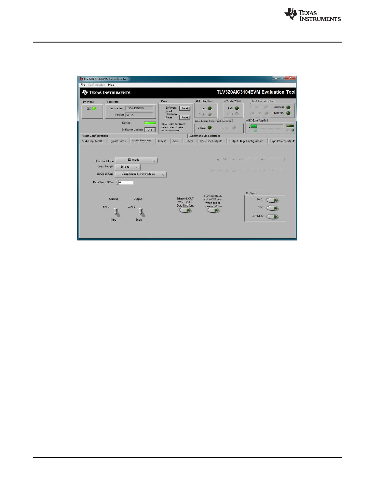
4.5 Audio Interface Tab
The Audio Interface tab, shown in Figure 11, allows configuration of the audio digital data interface to the
TLV320AIC3109-Q1.
www.ti.com
Figure 11. Audio Interface Tab
The interface mode may be selected using the Transfer Mode control—selecting either I2S mode, DSP
mode, or Right- or Left-Justified modes. Word length can be selected using the Word Length control, and
the bit clock rate can also be selected using the Bit Clock rate control. The Data Word Offset, used in
TDM mode (see TLV320AIC3109-Q1 Automotive, Low-Power, 96-kHz, Mono Audio Codec) can also be
selected on this tab.
Along the bottom of this tab are controls for choosing the BLCK and WCLK as being either inputs or
outputs. With the codec configured in Slave mode, both the BCLK and WCLK are set to inputs. If the
codec is in Master mode, then BCLK and WCLK are configured as outputs. Additionally, two buttons
provide the option for placing the DOUT line in a 3-state mode when there is not valid data and
transmitting BLCK and WCLK when the codec is powered down.
Re-synchronization of the audio bus is enabled using the controls in the lower right corner of this screen.
Re-synchronization is done if the group delay changes by more than ±FS / 4 for the ADC or DAC sample
rates (see TLV320AIC3109-Q1 Automotive, Low-Power, 96-kHz, Mono Audio Codec). The channels can
be soft muted when doing the re-sync if the Soft Mute button is enabled.
The default mode for the EVM is configured as 44.1 kHz, 16-bit, I2S words, and the codec is a slave
(BCLK and WCLK are supplied to the codec externally). For use with the PC software and the USBMODEVM, the default settings should be used; no change to the software is required.
18
TLV320AIC3109EVM-K
Copyright © 2017, Texas Instruments Incorporated
SLAU738–September 2017
Submit Documentation Feedback
Page 19
www.ti.com
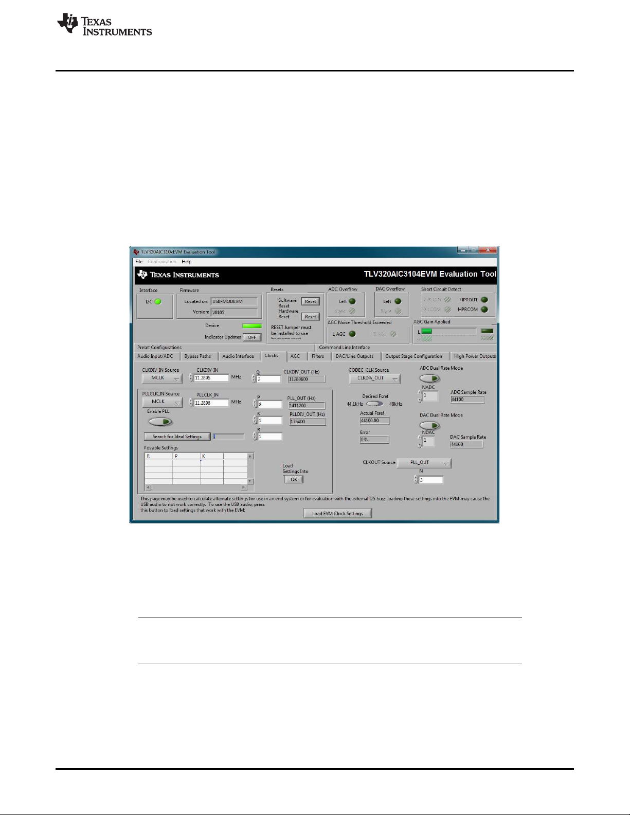
4.6 Clocks Tab
The TLV320AIC3109-Q1 provides a phase-locked loop (PLL) that allows flexibility in the clock generation
for the ADC and DAC sample rates. The Clocks tab contains the controls used to configure the
TLV320AIC3109-Q1 for operation with a wide range of master clocks. See the Audio Clock Generation
Processing figure in TLV320AIC3109-Q1 Automotive, Low-Power, 96-kHz, Mono Audio Codec for further
details of selecting the correct clock settings.
For use with the PC software and the USB-MODEVM, the clock settings must be set a certain way. If the
settings are changed from the default settings which allow operation from the USB-MODEVM clock
reference, the EVM settings can be restored automatically by pushing the Load EVMS Clock Settings
button at the bottom of this tab. Note that changing any of the clock settings from the values loaded when
this button is pushed may result in the EVM not working properly with the PC software or USB interface. If
an external audio bus is used (audio not driven over the USB bus), then settings may be changed to any
valid combination. The Clocks tab is shown in Figure 12.
TLV320AIC3109EVM Software
Figure 12. Clocks Tab
4.6.1 Configuring the Codec Clocks and Fsref Calculation
The codec clock source is chosen by the CODEC_CLK Source control. When this control is set to
CLKDIV_OUT, the PLL is not used; when set to PLLDIV_OUT, the PLL is used to generate the clocks.
NOTE: Per TLV320AIC3109-Q1 Automotive, Low-Power, 96-kHz, Mono Audio Codec, the codec
should be configured to allow the value of Fsref to fall between the values of 39 kHz to
53 kHz.
SLAU738–September 2017
Submit Documentation Feedback
Copyright © 2017, Texas Instruments Incorporated
TLV320AIC3109EVM-K
19
Page 20

TLV320AIC3109EVM Software
4.6.1.1 Use Without PLL
Setting up the TLV320AIC3109-Q1 for clocking without using the PLL permits the lowest power
consumption by the codec. The CLKDIV_IN source can be selected as either MCLK, GPIO2, or BCLK,
the default is MCLK. The CLKDIV_IN frequency is then entered into the CLKDIV_IN box, in megahertz
(MHz). The default value shown, 11.2896 MHz, is the frequency used on the USB-MODEVM board. This
value is then divided by the value of Q, which can be set from 2 to 17; the resulting CLKDIV_OUT
frequency is shown in the indicator next to the Q control. The result frequency is shown as the Actual
Fsref.
4.6.1.2 Use With The PLL
When PLLDIV_OUT is selected as the codec clock source, the PLL is used. The PLL clock source is
chosen using the PLLCLK_IN control, and may be set to either MCLK, GPIO2, or BCLK. The PLLCLK_IN
frequency is then entered into the PLLCLK_IN Source box.
The PLL_OUT and PLLDIV_OUT indicators show the resulting PLL output frequencies with the values set
for the P, K, and R parameters of the PLL. See TLV320AIC3109-Q1 Automotive, Low-Power, 96-kHz,
Mono Audio Codec for an explanation of these parameters. The parameters can be set by clicking on the
up or down arrows of the P, K, and R combo boxes, or they can be typed into these boxes.
The values can also be calculated by the PC software. To use the PC software to find the ideal values of
P, K, and R for a given PLL input frequency and desired Fsref:
1. Verify the correct reference frequency is entered into the PLLCLK_IN Source box in megahertz
(MHz).
2. The desired Fsref should be set using the Fsref switch.
3. Push the Search for Ideal Settings button. The software will start searching for ideal combinations of
P, K, and R which achieve the desired Fsref. The possible settings for these parameters are displayed
in the spreadsheet-like table illustrated in Figure 12, labeled Possible Settings.
4. Click on a row in this table to select the P, K, and R values located in that row. Notice that when this is
done, the software updates the P, K, R, PLL_OUT, and PLLDIV_OUT readings, as well as the Actual
Fsref and Error displays. The values show the calculations based on the values that were selected.
This process does not actually load the values into the TLV320AIC3109-Q1; however, it only updates
the displays in the software. If more than one row exists, the user can choose the other rows to see
which of the possible settings comes closest to the ideal settings.
When a suitable combination of P, K, and R have been chosen, pressing the Load Settings into Device?
button will download these values into the appropriate registers on the TLV320AIC3109-Q1.
www.ti.com
4.6.1.3 Setting the ADC and DAC Sampling Rates
The Fsref frequency that is determined by either enabling or bypassing the PLL (see Section 4.6.1.1 or
Section 4.6.1.2) is used to set the actual ADC and DAC sampling rates. Using the NADC and NDAC
factors, the sampling rates are derived from the Fsref. If dual-rate mode is desired, this option can be
enabled for either the ADC or DAC by pressing the corresponding Dual Rate Mode button. The ADC and
DAC sampling rates are shown in the box to the right of each control.
20
TLV320AIC3109EVM-K
Copyright © 2017, Texas Instruments Incorporated
SLAU738–September 2017
Submit Documentation Feedback
Page 21
www.ti.com
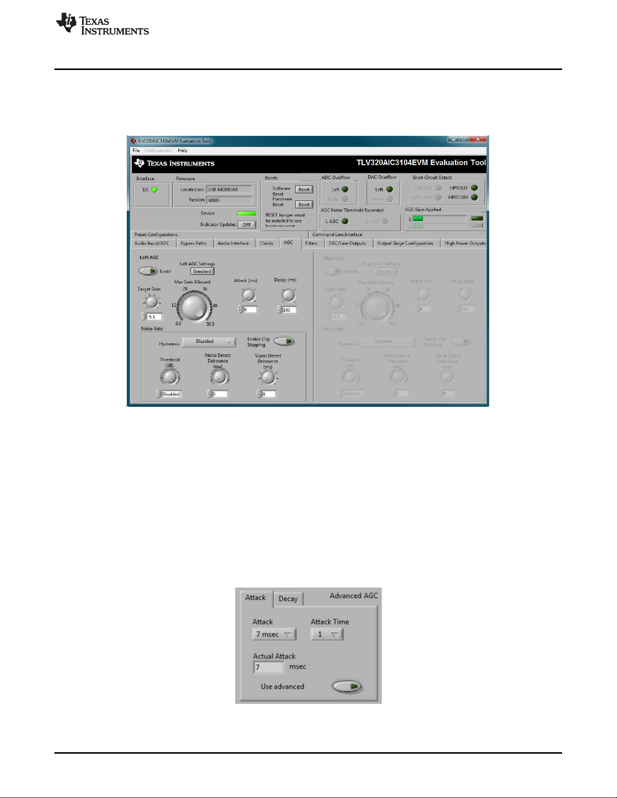
4.7 AGC Tab
The AGC tab consists a set of controls to configure the automatic Gain Control (AGC) of the
TLV320AIC3109-Q1. The AGC function is described in TLV320AIC3109-Q1 Automotive, Low-Power, 96-
kHz, Mono Audio Codec. The default AGC tab configuration is shown in Figure 13.
TLV320AIC3109EVM Software
Figure 13. AGC Tab
The AGC can be enabled using the Enable button. Target gain (dB), Attack time (milliseconds), Decay
time (milliseconds), and the Maximum PGA Gain Allowed (dB) can all be set, respectively, using the four
corresponding knobs.
The TLV320AIC3109-Q1 allows for the Attack and Decay times of the AGC to be set up in two different
modes, standard and advanced. The AGC Settings button determines the mode selection. The Standard
mode provides several preset times that can be selected by adjustments made to the Attack and Decay
knobs. If finer control over the times is required, then the Advanced mode should be selected. When the
Advanced mode is enabled, two tabs should appear that allow separate, advanced control of the Attack
and Delay times of the AGC (see Figure 14). These options allow selection of the base time as well as a
multiplier to achieve the actual times shown in the corresponding text box. The Use advanced button
should be enabled to program the registers with the correct values selected via the pull-down options for
base time and multiplier.
SLAU738–September 2017
Submit Documentation Feedback
Figure 14. Advanced AGC settings
Copyright © 2017, Texas Instruments Incorporated
TLV320AIC3109EVM-K
21
Page 22

TLV320AIC3109EVM Software
Noise gate functions, such as Hysteresis, Enable Clip stepping, Threshold (dB), Signal Detect
Debounce (ms), and Noise Detect Debounce (ms) are set using the corresponding controls in the
Noise Gate group box.
4.8 Filters Tab
The TLV320AIC3109-Q1 has an advanced feature set for applying digital filtering to audio signals. This
tab controls all of the filter features of the TLV320AIC3109-Q1. In order to use this tab and have plotting of
filter responses correct, the DAC sample rate must be set correctly. Therefore, the clocks must be set up
correctly in the software following the discussion in Section 4.6. The Filters tab is depicted in Figure 15.
www.ti.com
22
Figure 15. Filters Tab
The AIC3104 digital filtering is available to both the ADC and DAC. The ADC has optional high pass
filtering and allows the digital output from the ADC through digital effects filtering before exiting the codec
through the PCM interface. Likewise, the digital audio data can be routed through the digital effects
filtering before passing through the optional de-emphasis filter before the DAC. The digital effects filtering
can only be connected to either the ADC or DAC, not both at the same time.
The Filters tab is divided into several areas. The left side of the tab, is used to select between the DAC or
ADC filters and assist in the selection and calculating the desired filter coefficients. The right hand side of
the tab shows a frequency response plot of the digital effects filter selected and the coefficients that are
programmed into the device. The plots show the magnitude and phase response of each biquad section,
plus the combined responses of the two biquad filters. Note that the plot shows only the responses of the
effect filters, not the combined response of those filter along with the de-emphasis and ADC high-pass
filters.
TLV320AIC3109EVM-K
Copyright © 2017, Texas Instruments Incorporated
SLAU738–September 2017
Submit Documentation Feedback
Page 23

www.ti.com
4.8.1 ADC Filters
4.8.1.1 High Pass Filter
The TLV320AIC3109-Q1 ADC provides the option of enabling a high-pass filter, which helps to reduce the
effects of DC offsets in the system. The ADC high-pass filter tab is shown in Figure 16. This tab shows the
options for programming various filter associated with the ADC. The high-pass filter has two modes:
standard and programmable.
The standard high-pass filter option allows the selection of the high-pass filter frequency from several
preset options that can be chosen with the ADC HP Filter control. Four options are available for this filter
setting, one for disable and other three different corner frequencies which are based on the ADC sample
rate.
For custom filter requirements, the programmable function allows custom coefficients to achieve a
different filter than provided by the preset filters. The controls for the programmable high-pass filter are
located under the Programmable Filters heading. The process should use the following steps:
1. The filter coefficients can be entered in the HP Filter controls near the bottom of the tab.
2. Press the Download Coefficients button to download the coefficients to the codec registers.
3. Enable the Programmable High-Pass Filters by selecting the ADC button.
The programmable high-pass filter should now be correctly programmed and enabled. The ADC can now
be enabled with the high-pass filter.
TLV320AIC3109EVM Software
4.8.1.2 Digital Effects Filter - ADC
The ADC digital outputs stream can be routed through the digital effects filter in the codec to allow custom
audio performance. The digital effects filter cannot operate on both the ADC or DAC at the same time.
The digital effects filter operation is discussed in Section 4.8.3.
4.8.2 DAC Filters
The DAC Filters tab is shown in Figure 17. Detailed information about the different configuration options
for the DAC filters is discussed in the following sections.
Figure 16. ADC High Pass Filters
Figure 17. DAC Filters
SLAU738–September 2017
Submit Documentation Feedback
Copyright © 2017, Texas Instruments Incorporated
TLV320AIC3109EVM-K
23
Page 24

TLV320AIC3109EVM Software
4.8.2.1 De-emphasis Filters
The de-emphasis filters used in the TLV320AIC3109-Q1 can be programmed as described in
TLV320AIC3109-Q1 Automotive, Low-Power, 96-kHz, Mono Audio Codec, using this tab. Enter the
coefficients for the de-emphasis filter response desired. While on this tab, the de-emphasis response is
shown on the Effect Filter Response graph; however, note that this response is not included in graphs of
other effect responses when on the other filter design tabs.
4.8.2.2 DAC Digital Effects Filter
The digital audio input stream can be routed through the digital effects filter in the codec before routing to
the DAC to allow custom audio performance. The digital effects filter cannot operate on both the ADC or
DAC at the same time. The digital effects filter operation is discussed in Section 4.8.3.
www.ti.com
Figure 18. De-emphasis Filters
4.8.3 Digital Effects Filters
The digital effect filters (or biquad filters) of the TLV320AIC3109-Q1 are selected using the check boxes
shown in the Figure 17 tab. The De-emphasis filters are described in TLV320AIC3109-Q1 Automotive,
Low-Power, 96-kHz, Mono Audio Codec, and their coefficients may be changed.
When designing filters for use with TLV320AIC3109-Q1, the software allows for several different filter
types to be used. These options are shown on a tab control in the lower left corner of the screen. When a
filter type is selected, and suitable input parameters defined, the response is shown in the Effect Filter
Response graph. Regardless of the setting for enabling the Effect Filter, the filter coefficients are not
loaded into the TLV320AIC3109-Q1 until the Download Coefficients button is pressed. To avoid noise
during the update of coefficients, it is recommended for the user to uncheck the Effect Filter check box
before downloading coefficients. Once the desired coefficients are in the TLV320AIC3109-Q1, enable the
filters by checking the Effect Filters box again.
4.8.3.1 Shelf Filters
A shelf filter is a simple filter that applies a gain (positive or negative) to frequencies above or below a
certain corner frequency. As shown in Figure 19, in Bass mode a shelf filter applies a gain to frequencies
below the corner frequency; in Treble mode the gain is applied to frequencies above the corner frequency.
24
TLV320AIC3109EVM-K
Copyright © 2017, Texas Instruments Incorporated
SLAU738–September 2017
Submit Documentation Feedback
Page 25

www.ti.com
To use these filters, enter the gain desired and the corner frequency. Choose the mode to use (Bass or
Treble); the response is plotted on the Effect Filter Response graph.
4.8.3.2 EQ Filters
EQ, or parametric filters can be designed on this tab, as shown in Figure 20). Enter a gain, bandwidth,
and a center frequency (Fc). Either bandpass (positive gain) or band-reject (negative gain) filters can be
created
TLV320AIC3109EVM Software
Figure 19. Shelf Filters
4.8.3.3 Analog Simulation Filters
Biquads are quite good at simulating analog filter designs. For each biquad section on this tab, enter the
desired analog filter type to simulate (Butterworth, Chebyshev, Inverse Chebyshev, Elliptic, or Bessel).
Parameter entry boxes appropriate to the filter type are shown (ripple, for example, with Chebyshev filters,
and so forth). Enter the desired design parameters and the response is shown. The Analog Simulation
Filters tab is shown in Figure 21.
SLAU738–September 2017
Submit Documentation Feedback
Figure 20. EQ Filters
Copyright © 2017, Texas Instruments Incorporated
TLV320AIC3109EVM-K
25
Page 26

TLV320AIC3109EVM Software
4.8.3.4 Preset Filters
Many applications are designed to provide preset filters common for certain types of program material.
The Preset Filters tab, as shown in Figure 22, allows selection of one of four preset filter responses Rock, Jazz, Classical, or Pop.
www.ti.com
Figure 21. Analog Simulation Filters
4.8.3.5 User Filters
If filter coefficients are known, they can be entered directly on this tab for both biquads. The filter response
will not be shown on the Effect Filter Response graph for user filters. The User Filters tab is depicted in
Figure 23.
26
TLV320AIC3109EVM-K
Figure 22. Preset Filters
Figure 23. User Filters
Copyright © 2017, Texas Instruments Incorporated
SLAU738–September 2017
Submit Documentation Feedback
Page 27

www.ti.com
4.8.3.6 3-D Effect
The 3-D Effect is described in TLV320AIC3109-Q1 Automotive, Low-Power, 96-kHz, Mono Audio Codec.
The 3-D effect uses the two biquad sections in a different way than most other effect filter settings. To use
this effect properly, make sure the appropriate coefficients are already loaded into the two biquad
sections. The User Filters tab may be used to load the coefficients. Figure 24 shows the 3-D Effect tab.
To enable the 3-D effect, check the 3-D Effect On box. The Depth knob controls the value of the 3-D
Attenuation Coefficient.
TLV320AIC3109EVM Software
Figure 24. 3D Effect Settings
4.9 Output Stage Configuration Tab
The Output Stage Configuration tab (shown in Figure 25) allows the setting of different features of the
output drivers.
SLAU738–September 2017
Submit Documentation Feedback
Figure 25. Output Stage Configuration Tab
Copyright © 2017, Texas Instruments Incorporated
TLV320AIC3109EVM-K
27
Page 28

TLV320AIC3109EVM Software
The Configuration control may be set as either Fully-Differential or Pseudo-Differential. This control is
used to determine if the output stage is being used to drive a fully differential output load or a output load
where one of the outputs if referenced to a common-mode voltage (pseudo-differential).
The output Coupling control can be chosen as either Capless or AC-coupled. This setting should
correspond to the setting of the hardware switch (SW1) on the TLV320AIC3109EVM (CAPLESS or CAP).
The common mode voltage of the outputs may be set to 1.35 V, 1.5 V, 1.65 V, or 1.8 V using the
Common Mode Voltage control.
The TLV320AIC3109-Q1 offers several options to help reduce the turnon and turnoff pop of the output
amplifiers. The Power-On Delay of the output drivers can be set using the corresponding control from 0's
up to 4 seconds. Ramp-Up Step Timing can also be adjusted from 0ms to 4ms. The outputs can be set
to soft-step their volume changes, using the Output Volume Soft Stepping control, and set to step once
per Fs period, once per two Fs periods, or soft-stepping can be disabled altogether.
The high-power outputs of the TLV320AIC3109-Q1 can be configured to go to a weak common-mode
voltage when powered down. The source of this weak common-mode voltage can be set on this tab with
the Weak Output CM Voltage Source drop-down. Choices for the source are either a resistor divider off
the AVDD_DAC supply, or a bandgap reference. Refer to TLV320AIC3109-Q1 Automotive, Low-Power,
96-kHz, Mono Audio Codec for more details on this option.
Headset detection features are enabled using the Enable button in the Headset Detection group box.
When enabled, the indicators in the HS/Button Detect group box will light when either a button press or
headset is detected. When a headset is detected, the type of headset is displayed in the Detection Type
indicator. Debounce times for detection are set using the Jack Detect Debounce and Button Press
Debounce controls, which offer debounce times in different numbers of milliseconds. Refer to
TLV320AIC3109-Q1 Automotive, Low-Power, 96-kHz, Mono Audio Codec for more information regarding
headset detection.
Output short-circuit protection can be enabled in the Short Circuit Protection group box. Short Circuit
Protection can use a current-limit mode, where the drivers will limit current output if a short-circuit
condition is detected, or in a mode where the drivers will power down when such a condition exists.
The I2C Bus Error Detection button allows the user to enable circuitry which will set a register bit
(Register 107, D0) if an I2C bus error is detected.
www.ti.com
4.10 DAC/Line Outputs Tab
The DAC/Line Outputs tab controls the DAC power and volume, as well as routing of digital data to the
DAC and the analog line output from the DAC. The default configuration of the DAC/Line Outputs tab is
shown in Figure 26.
28
TLV320AIC3109EVM-K
Copyright © 2017, Texas Instruments Incorporated
SLAU738–September 2017
Submit Documentation Feedback
Page 29

www.ti.com
TLV320AIC3109EVM Software
Figure 26. DAC/Line Outputs Tab
4.10.1 DAC Controls
On the left side of this tab are controls for the DAC.
In similar fashion as the ADC, the DAC controls are set to allow control over the powering and volume
setting of the DAC. The DAC volume level can be set by using the Volume knob.
The data from the audio serial interface used by the DAC is selected using the drop-down boxes under
the DAC Datapath. The DAC channel can be selected to be off, use left channel data, use right channel
data, or use a mono mix of the left and right data.
Analog audio coming from the DACs is routed to outputs using the Output Path controls in DAC control
panel. The DAC output can be mixed with the analog inputs (PGA_L, PGA_R) and routed to the Line or
High Power outputs using the mixer controls for these outputs on this tab (for the line outputs) or on the
High Power Outputs tab (for the high power outputs). If the DAC is to be routed directly to either the Line
or HP outputs, these can be selected as choices in the Output Path control. Note that if the Line or HP
outputs are selected as the Output Path, the mixer controls on this tab and the High Power Output tabs
have no effect.
4.10.2 Line Output Mixers
On the right side of this tab are horizontal panels where the analog output mixing functions for the line
outputs are located.
Each line output master volume is controlled by the knob at the far right of these panels, below the line
output labels. The output amplifier gain can be muted or set at a value between 0 and 9 dB in 1-dB steps.
Power/Enabled status for the line output can also be controlled using the button below this master output
knob (Powered Up).
If the DAC Output Path control is set to Mix with Analog Inputs, the knobs in each panel can be used to
set the individual level of signals routed and mixed to the line output. PGA_L, PGA_R, and DAC_L levels
can each be set to create a custom mix of signals presented to that particular line output.
NOTE: If the DAC Output Path control is set to anything other than Mix with Analog Inputs, these
controls have no effect.
SLAU738–September 2017
Submit Documentation Feedback
Copyright © 2017, Texas Instruments Incorporated
TLV320AIC3109EVM-K
29
Page 30

TLV320AIC3109EVM Software
4.11 High-Power Outputs Tab
www.ti.com
The High-Power Outputs tab contains horizontal groupings of controls, one for each one of the high power
outputs. Each output has a mixer to mix the PGA_L, PGA_R, and DAC_L signals, assuming that the
DACs are not routed directly to the high power outputs. The High-Power Outputs tab is shown in
Section 4.10.
At the left of each output strip is a Powered Up button that controls whether the corresponding output is
powered up or not. The When powered down button allows the outputs to be tri-stated or driven weakly
to the output common mode voltage.
The HPCOM output can be used as an independent output channel or can be used as a complementary
signal to the HPOUT output. In these complementary configurations, the HPCOM output can be selected
as Differential of HPOUT signal to the HPOUT output or may be set to be a common mode voltage
(Constant VCM Out). When used in these configurations, the Powered Up button for the HPCOM output
is disabled, as the power mode for that output will track the power status of the HPOUT output. The
selection of Differential of HPLCOM or Ext. Feedback/HPLCOM constant VCM should not be selected for
the TLV320AIC3109EVM evaluation.
At the right side of the output strip is a master volume knob for that output, which allows the output
amplifier gain to be muted or set from 0 to 9 dB in 1-dB steps.
4.12 Preset Configurations Tab
The Preset Configurations tab should be ignored for the evaluation of the TLV320AIC3109-Q1 as the
configuration used in that tab is relevant for the TLV320AIC3104 device only. Scripts for the correct
configuration of the TLV320AIC3109EVM are included in Appendix H. These scripts can be loaded into
the EVM by using the Command Line Interface tab, shown in Figure 28.
Figure 27. High-Power Outputs Tab
30
TLV320AIC3109EVM-K
Copyright © 2017, Texas Instruments Incorporated
SLAU738–September 2017
Submit Documentation Feedback
Page 31

www.ti.com
4.13 Command Line Interface Tab
A simple scripting language controls the TAS1020 on the USB-MODEVM from the LabVIEW™ based PC
software. The main program controls, described previously, do nothing more than write a script which is
then handed off to an interpreter that sends the appropriate data to the correct USB endpoint. Because
this system is script-based, provision is made in this tab for the user to view the scripting commands
created as the controls are manipulated, as well as load and execute other scripts that have been written
and saved. The Command Line Interface tab is shown in Figure 28. This design allows the software to
be used as a quick test tool or to help provide troubleshooting information in the rare event that the user
encounters problem with this EVM.
TLV320AIC3109EVM Software
A script is loaded into the command buffer, either by operating the controls on the other tabs or by loading
a script file. When executed, the return packets of data which result from each command is displayed in
the Read Data array control. When executing several commands, the Read Data control shows only the
results of the last command. To see the results after every executed command, use the logging function
described in the following paragraphs.
The File menu depicted in Figure 29 provides some options for working with scripts. The first option, Open
Command File..., loads a command file script into the command buffer. This script can then be executed
by pressing the Execute Command Buffer button.
The second option, Save Command File..., opens a save dialog box and then saves the text loaded in the
Command Buffer into a text file defined by the user.
The third option is Log Script and Results..., which opens a file save dialog box. Choose a location for a
log file to be written using this file save dialog. When the Execute Command Buffer button is pressed,
the script runs and the script, along with resulting data read back during the script, will be saved to the file
specified. The log file is a standard text file that can be opened with any text editor, and looks much like
the source script file, but with the additional information of the result of each script command executed.
SLAU738–September 2017
Submit Documentation Feedback
Figure 28. Command Line Interface Tab
Copyright © 2017, Texas Instruments Incorporated
TLV320AIC3109EVM-K
31
Page 32

TLV320AIC3109EVM Software
Under the Help menu is an About... menu item which displays information about the TLV320AIC3109EVM
software.
The actual USB protocol used as well as instructions on writing scripts are detailed in the following
subsections. While it is not necessary to understand or use either the protocol or the scripts directly,
understanding them may be helpful to some users.
www.ti.com
Figure 29. File Menu
32
TLV320AIC3109EVM-K
Copyright © 2017, Texas Instruments Incorporated
SLAU738–September 2017
Submit Documentation Feedback
Page 33

EVM Connector Descriptions
A.1 Analog Interface Connectors
This appendix contains the connection details for each of the main header connectors on the EVM.
A.1.1 Analog Dual-Row Header Details (J13 and J14)
For maximum flexibility, the TLV320AIC3109EVM is designed for easy interfacing to multiple analog
sources. Table 6 summarizes the analog interface pinout for the TLV320AIC3109EVM.
Table 6. Analog Interface Pinout
Pin Number Signal Description
J1.1 NC Not connected
J1.2 NC Not connected
J1.3 HPCOM High-power output driver (minus or multifunctional)
J1.4 HPOUT High-power output driver (plus)
J1.5 LINE1M MIC1 or LINE1 analog input (minus or multifunctional)
J1.6 LINE1P MIC1 or LINE1 analog input (plus or multifunctional)
J1.7 LINE2M MIC2 or LINE2 analog input (minus or multifunctional)
J1.8 LINE2P MIC2 or LINE2 analog input (plus or multifunctional)
J1.9 AGND Analog ground
J1.10 NC Not connected
J1.11 AGND Analog ground
J1.12 NC Not connected
J1.13 AGND Analog ground
J1.14 MICBIAS Microphone bias voltage output
J1.15 NC Not connected
J1.16 MICDET Microphone Detect
J1.17 AGND Analog ground
J1.18 NC Not connected
J1.19 AGND Analog ground
J1.20 NC Not connected
J2.1 NC Not connected
J2.2 NC Not connected
J2.3 NC Not connected
J2.4 NC Not connected
J2.5 NC Not connected
J2.6 NC Not connected
J2.7 LEFT_LOP Left-line output (plus)
J2.8 LEFT_LOM Left-line output (minus)
J2.9 AGND Analog ground
J2.10 RIGHT_LOP Right-line output (plus)
J2.11 AGND Analog ground
J2.12 RIGHT_LOM Right-line output (minus)
J2.13 AGND Analog ground
J2.14 NC Not connected
Appendix A
SLAU738–September 2017
SLAU738–September 2017
Submit Documentation Feedback
Copyright © 2017, Texas Instruments Incorporated
EVM Connector Descriptions
33
Page 34

Analog Interface Connectors
Table 6. Analog Interface Pinout (continued)
Pin Number Signal Description
J2.15 NC Not connected
J2.16 NC Not connected
J2.17 AGND Analog ground
J2.18 NC Not connected
J2.19 AGND Analog ground
J2.20 NC Not connected
A.1.2 Analog Screw Terminal Details (J1-5 and J8-12)
In addition to the analog headers, the analog inputs and outputs can also be accessed through alternate
connectors, either screw terminals or audio jacks. The mono microphone is also tied to J13 and the mono
headphone output is available at J16.
Table 7 summarizes the screw terminals available on the TLV320AIC3109EVM.
Table 7. Alternate Analog Connectors
Designator Pin 1 Pin 2 Pin 3
J6 External mic bias source (+) External mic bias source (GND)
J10 LINE2 (+) LINE2 (–) AGND
J13 LINE1 (+) LINE1 (–) AGND
J17 AGND HPCOM (–) HPOUT (+)
J20 LEFT OUT (+) LEFT OUT (–)
J21 RIGHT OUT (+) RIGHT OUT (–)
www.ti.com
34
EVM Connector Descriptions
Copyright © 2017, Texas Instruments Incorporated
SLAU738–September 2017
Submit Documentation Feedback
Page 35

www.ti.com
A.2 Digital Interface Connectors (J16 and J17)
The TLV320AIC3109EVM is designed to easily interface with multiple control platforms. Table 8
summarizes the digital interface pinout for the TLV320AIC3109EVM.
Table 8. Digital Interface Pinout
Pin Number Signal Description
J4.1 NC Not connected
J4.2 NC Not connected
J4.3 SCLK SPI serial clock
J4.4 DGND Digital ground
J4.5 NC Not connected
J4.6 NC Not connected
J4.7 NC Not connected
J4.8 RESET
INPUT
J4.9 NC Not connected
J4.10 DGND Digital ground
J4.11 NC Not connected
J4.12 NC Not connected
J4.13 NC Not connected
J4.14 RESET Reset
J4.15 NC Not connected
J4.16 SCL I2C serial clock
J4.17 NC Not connected
J4.18 DGND Digital ground
J4.19 NC Not connected
J4.20 SDA I2C serial data I/O
J5.1 NC Not connected
J5.2 NC Not connected
J5.3 BCLK Audio serial data bus bit clock (I/O)
J5.4 DGND Digital ground
J5.5 NC Not connected
J5.6 NC Not connected
J5.7 WCLK Audio serial data bus word clock (I/O)
J5.8 NC Not connected
J5.9 NC Not connected
J5.10 DGND Digital ground
J5.11 DIN Audio serial data bus data input (input)
J5.12 NC Not connected
J5.13 DOUT Audio serial data bus data output (output)
J5.14 NC Not connected
J5.15 NC Not connected
J5.16 SCL I2C serial clock
J5.17 MCLK Master clock input
J5.18 DGND Digital ground
J5.19 NC Not connected
J5.20 SDA I2C Serial Data I/O
Reset signal input to EVM
Digital Interface Connectors (J16 and J17)
SLAU738–September 2017
Submit Documentation Feedback
Copyright © 2017, Texas Instruments Incorporated
EVM Connector Descriptions
35
Page 36

Power Supply Connector Pin Header, J3
Note that J5 comprises the signals needed for an I2S serial digital audio interface; the control interface (I2C
and RESET) signals are routed to J4. I2C is actually routed to both connectors; however, the device is
connected only to J4.
A.3 Power Supply Connector Pin Header, J3
J3 provides connection to the common power bus for the TLV320AIC3109EVM. Power is supplied on the
pins listed in Table 9.
Table 9. Power Supply Pinout
Signal Pin Number Signal
NC J3.1 J3.2 NC
+5VA J3.3 J3.4 NC
DGND J3.5 J3.6 AGND
+1.8VD J3.7 J3.8 NC
+3.3VD J3.9 J3.10 NC
The TLV320AIC3109EVM motherboard (the USB-MODEVM Interface board) supplies power to J3 of the
TLV320AIC3109EVM. Power for the motherboard is supplied either through its USB connection or via
terminal blocks on that board.
www.ti.com
36
EVM Connector Descriptions
Copyright © 2017, Texas Instruments Incorporated
SLAU738–September 2017
Submit Documentation Feedback
Page 37

TLV320AIC3109EVMDC006 Rev A
100
R5
100
R6
100
R7
100
R8
100
R9
100
R12
0.1µF
C19
0.1µF
C16
0.1µF
C14
0.047µF
C24
0.047µF
C25
0.047µF
C26
0.047µF
C27
0.047µF
C28
0.047µF
C29
1
2
J20
1
2
J21
1
2
3
J10
1
2
3
J13
J8
J19
J18
1
2
MK1
123
456
SW1
TP15
IN1P
TP17
IN1M
TP22
MICDET
TP27
AVSS
TP16
HPOUT
TP28
DRVSS
TP21
HPCOM
TP20
IN2P
TP24
IN2M
TP18
HPOUT_LPF
TP19
HPCOM_LPF
AGNDAGND DGND DGND
AGNDAGND DGNDDGND
DVDDAVDD
IOVDDDRVDD
AGND DGND AGND
AGND
AGND
AGND
AGND
TP32
RIGHT_LOP
TP34
RIGHT_LOM
TP25
LEFT_LOP
TP29
LEFT_LOM
LEFT+
LEFT-
RIGHT+
RIGHT-
RIGHT OUT
LEFT OUT
IN1M
IN1P
AGND
AGND
IN2M
IN2P
AGND
AGND
1
2
3
J7
AGND
MICBIAS
AGND
AGND
AGND AGND
AGND
AGND
AGND
HPOUT
HPCOM
AGND
2.7k
R3
2.7k
R4
100k
R2
TP11
AVDD
TP12
DVDD
TP13
DRVDD
TP14
IOVDD
1
2
J6
J15
J14
J12
J11
TP33
RIGHT+
TP35
RIGHT-
TP26
LEFT+
TP30
LEFT-
MCLK
1
BCLK
2
WCLK
3
DIN
4
DOUT
5
DVSS
6
IOVDD
7
SCL
8
SDA
9
MIC1P/LINE1P
10
MIC1M/LINE1M
11
MIC2P/LINE2P
12
MIC2M/LINE2M
13
MICDET
14
MICBIAS
15
NC
16
AVSS
17
DRVDD
18
NC
19
NC
20
DRVSS
21
HPCOM
22
HPOUT
23
DRVDD
24
AVDD
25
AVSS
26
LEFT_LOP
27
LEFT_LOM
28
RIGHT_LOP
29
RIGHT_LOM
30
RESET
31
DVDD
32
PAD
33
U3
TLV320AIC3109-Q1
1
2
3
J17
AGND
EXTERNAL
10µF
C18
10µF
C20
10µF
C13
10µF
C15
0.1µF
C17
0.1µF
C7
0.1µF
C8
0.1µF
C9
0.1µF
C10
10µF
C6
C11
C12
0
R11
2.2k
R10
47µF
C22
47µF
C23
47µF
C21
TP31
MICBIASIN
TP23
MICBIAS
IOVDD_IN
3
2
1
J9
3
2
1
J16
IN 1
IN 2
HEADPHONE
HEADPHONE
CAPLESS AC-COUPLED
TLV30AIC3109-Q1 CIRCUIT
MICROPHONE
RESET
SDA
SCL
MCLK
WCLK
BCLK
DOUT
DIN
MICBIAS SELECTION
ON-BOARDMIC
ENABLE
JACK
JACK
MICBIAS
OUT
Copyright © 2017, Texas Instruments Incorporated
B.1 Main Schematics
Figure 30 illustrates the main TLV320AIC3109-Q1 schematics.
Appendix B
SLAU738–September 2017
TLV320AIC3109EVM Schematic
SLAU738–September 2017
Submit Documentation Feedback
Figure 30. TLV320AIC3109-Q1 Main Schematics
Copyright © 2017, Texas Instruments Incorporated
TLV320AIC3109EVM Schematic
37
Page 38

TLV320AIC3109EVMDC006 Rev A
0.1µF
C3
0.1µF
C30
A0
1
A1
2
A2
3
VSS4SDA
5
SCL
6
WP
7
VCC
8
U2
24LC512-I/ST
1 2
3 4
5 6
7 8
9 10
11 12
13 14
15
17
19
16
18
20
J1A
1 2
3 4
5 6
7 8
9 10
11 12
13 14
15
17
19
16
18
20
J2A
1 2
3 4
5 6
7 8
9 10
11 12
13 14
15
17
19
16
18
20
J4A
1 2
3 4
5 6
7 8
9 10
11 12
13 14
15
17
19
16
18
20
J5A
1
3
5 6
4
2
7
9 10
8
1211
1413
1615
1817
2019
J1B
1
3
5 6
4
2
7
9 10
8
1211
1413
1615
1817
2019
J2B
1
3
5 6
4
2
7
9 10
8
1211
1413
1615
1817
2019
J5B
1
3
5 6
4
2
7
9 10
8
J3B
1 2
3 4
5 6
7 8
9 10
J3A
J30
2.7k
R1
10µF
C1
AGND AGND
+5VA
AGND
HPOUT
MICBIAS
HPCOM
AGND
LEFT+ LEFT-
RIGHT+
RIGHT-
AGND
DGND AGND
123
J22
IOVDD_IN +1.8VD +5VA+3.3VD
DGND
RESET
SDA
SCL
MCLK
WCLK
BCLK
DOUT
DIN
DGND
DGND
DGND DGND
IOVDD_INIOVDD_IN
DGND
SDA
SCL
HPOUT
IN1M
IN2M
MICBIAS
HPCOM
IN1P
IN2P
AGND
LEFT+ LEFT-
RIGHT+
RIGHT-
AGND
SDA
SCL
1
3
5 6
4
2
7
9 10
8
1211
1413
1615
1817
2019
J4B
DGND
RESET
SDA
SCL
DGND AGND
+5VA+3.3VD+1.8VD
MCLK
WCLK
BCLK
DOUT
DIN
DGND
SDA
SCL
RST
RST
AGND
+3.3VA
10µFC20.1µF
C4
+3.3VA
IOVDD_IN+3.3VA
+1.8VD DVDD
AVDD IOVDD
DRVDD
J25 J26
J27J24
+3.3V REGULATOR
J23
EEPROM
Secondary Circuits
TP8
DOUT
TP7
DIN
TP5
WCLK
TP6
BCLK
TP4
MCLK
TP1
RESET
TP2
SCL
TP3
SDA
RESET
SDA
SCL
MCLK
WCLK
BCLK
DOUT
DIN
USB-MODEVM INTERFACE
TEST POINTS
J1-1
J1-15
J1-2
J1-10
J1-12
J1-16
J1-18
J1-20
J1-2
J1-10
J1-12
J1-16
J1-18
J1-20
J1-1
J1-15
J4-1
J4-15
J4-3
J4-5
J4-7
J4-9
J4-11
J4-13
J4-17
J4-19
J4-12
J4-6
J4-2
J4-1
J4-15
J4-3
J4-5
J4-7
J4-9
J4-11
J4-13
J4-17
J4-19
J4-12
J4-6
J4-2
J5-1
J5-5
J5-9
J5-19
J5-15
J5-2
J5-6
J5-8
J5-12
J5-14
J5-1
J5-5
J5-9
J5-19
J5-15
J5-2
J5-6
J5-8
J5-12
J5-14
J3-1 J3-2
J3-4
J3-10
J3-8
J3-1 J3-2
J3-4
J3-10
J3-8
J2-1
J2-3
J2-5
J2-2
J2-4
J2-6
J2-14
J2-16
J2-18
J2-20
J2-1
J2-3
J2-5
J2-2
J2-4
J2-6
J2-14
J2-16
J2-18
J2-20
J2-15
J2-15
AGND
0.01µF
C5
AGND
J28
DGND
TP9
AGND
TP10
DGND
J29
CONNECTORS
IN1M
IN2M
IN1P
IN2P
OUT
1
NC
2
NR
3
GND
4
EN
5
NC
6
NC
7
IN
8
PAD
9
U1
TPS73533-Q1
AGND AGND
IOVDDSELECTION
Copyright © 2017, Texas Instruments Incorporated
Secondary Schematics
B.2 Secondary Schematics
Figure 31 illustrates the secondary TLV320AIC3109-Q1 schematics.
www.ti.com
38
TLV320AIC3109EVM Schematic
Figure 31. Connector, Test Points, and Power Distribution Schematics
Copyright © 2017, Texas Instruments Incorporated
Submit Documentation Feedback
SLAU738–September 2017
Page 39

DC006
A
PCB Number:
PCB Rev:
FID2FID1 FID3
FID5FID4 FID6
LOGO
PCB
Logo1
Texas Instruments
LOGO
PCB
Logo2
Pb-Free Symbol
LOGO
PCB
Logo3
FCC disclaimer
Assembly Note
ZZ2
These assemblies are ESD sensitive, ESD precautions shall be observed.
Assembly Note
ZZ3
These assemblies must be clean and free from flux and all contaminants. use of no clean flux is not acceptable.
Assembly Note
ZZ1
These assemblies must comply with workmanship standards IPC-A-610 Class 2, unless otherwise speci fied.
SH1 SH2 SH3 SH4
SH5 SH6 SH7 SH8
SH9 SH10 SH11
TLV320AIC3109-Q1 Evaluation Module DC006 RevA
HARDWARE
SHUNTS
SH12
Copyright © 2017, Texas Instruments Incorporated
www.ti.com
B.3 Hardware Schematics
Figure 32 illustrates the TLV320AIC3109-Q1 hardware.
Hardware Schematics
Figure 32. TLV320AIC3109EVM Hardware
SLAU738–September 2017
Submit Documentation Feedback
Copyright © 2017, Texas Instruments Incorporated
TLV320AIC3109EVM Schematic
39
Page 40

Appendix C
SLAU738–September 2017
TLV320AIC3109EVM Layout Views
The board layouts for the modular TLV320AIC3109EVM are illustrated in Figure 33 through Figure 38.
Figure 33. TLV320AIC3109EVM Assembly Layer
Figure 34. TLV320AIC3109EVM Top Layer
40
TLV320AIC3109EVM Layout Views
Copyright © 2017, Texas Instruments Incorporated
SLAU738–September 2017
Submit Documentation Feedback
Page 41

www.ti.com
Appendix C
Figure 35. TLV320AIC3109EVM Ground Layer
SLAU738–September 2017
Submit Documentation Feedback
Figure 36. TLV320AIC3109EVM Power Layer
TLV320AIC3109EVM Layout Views
Copyright © 2017, Texas Instruments Incorporated
41
Page 42

Appendix C
www.ti.com
Figure 37. TLV320AIC3109EVM Bottom Layer
42
Figure 38. TLV320AIC3109EVM Bottom Assembly Layer
TLV320AIC3109EVM Layout Views
Copyright © 2017, Texas Instruments Incorporated
SLAU738–September 2017
Submit Documentation Feedback
Page 43

Appendix D
SLAU738–September 2017
TLV320AIC3109EVM Bill of Materials
The complete bill of materials for the modular TLV320AIC3109EVM is provided in Table 10.
Table 10. TLV320AIC3109EVM Bill of Materials
# Designator Qty Value Part Number Manufacturer Description Package Reference
1 !PCB101 1 DC006 Any Printed Circuit Board
2 C1, C2 2 10uF C3216X5R1H106K160AB TDK CAP, CERM, 10 µF, 50 V, ±±10%, X5R, 1206 1206
3 C3, C4, C14,
C16, C17, C19,
C30
4 C5 1 0.01uF GRM188R71C103KA01D Murata CAP, CERM, 0.01 µF, 16 V, ±10%, X7R, 0603 0603
5 C6, C13, C15,
C18, C20
6 C7, C8, C9, C10 4 0.1uF C2012X7R1H104K085AA TDK CAP, CERM, 0.1 µF, 50 V, ±10%, X7R, 0805 0805
7 C21, C22, C23 3 47uF C3216X5R1C476M160AB TDK CAP, CERM, 47 µF, 16 V, ±15%, X5R, 1206 1206
8 C24, C25, C26,
C27, C28, C29
9 J1A, J2A, J4A,
J5A
10 J1B, J2B, J4B,
J5B
11 J3A 1 TSM-105-01-L-DV Samtec Header, 2.54mm, 5x2, Gold, SMT Header, 2.54mm, 5x2,
12 J3B 1 SSW-105-22-F-D-VS-K Samtec Connector, Header, 10-Pos (5x2), Receptacle,
13 J6, J20, J21 3 ED555/2DS On-Shore Technology Terminal Block, 3.5mm Pitch, 2x1, TH 7.0x8.2x6.5mm
14 J7, J22 2 TSW-103-07-G-S Samtec Header, 100mil, 3x1, Gold, TH 3x1 Header
15 J8, J11, J12,
J14, J15, J18,
J19, J23, J24,
J25, J26, J27,
J28, J29, J30
16 J9, J16 2 MJ1-3510-SMT-TR CUI Inc. Audio Jack, 3.5mm, Mono, R/A, Black, SMT Audio Jack, 3.5mm,
17 J10, J13, J17 3 ED555/3DS On-Shore Technology Terminal Block, 3.5mm Pitch, 3x1, TH 10.5x8.2x6.5mm
18 MK1 1 CMA-4544PF-W CUI Inc. Microphone, Electret Condenser, Omnidirectional, -44
19 R1, R3, R4 3 2.7k CRCW06032K70JNEA Vishay-Dale RES, 2.7 k, 5%, 0.1 W, 0603 0603
20 R2 1 100k RC0603FR-07100KL Yageo America RES, 100 k, 1%, 0.1 W, 0603 0603
21 R5, R6, R7, R8,
R9, R12
22 R10 1 2.2k CRCW08052K20JNEA Vishay-Dale RES, 2.2 k, 5%, 0.125 W, 0805 0805
23 R11 1 0 CRCW08050000Z0EA Vishay-Dale RES, 0, 5%, 0.125 W, 0805 0805
24 SH1, SH2, SH3,
SH4, SH5, SH6,
SH7, SH8, SH9,
SH10, SH11,
SH12
25 SW1 1 SSB22 TE Connectivity Switch, Slide, DPDT, On-On, 0.1 A, 30 V, TH TH, 6-Leads, Body
26 TP9, TP10 2 5011 Keystone Test Point, Multipurpose, Black, TH Black Multipurpose
27 U1 1 TPS73533-Q1 Texas Instruments 500-mA, Low Quiescent Current, Low-Noise, High
28 U2 1 24LC512-I/ST Microchip EEPROM, 512KBIT, 400KHZ, 8TSSOP TSSOP-8
7 0.1uF C1608X7R1H104K080AA TDK CAP, CERM, 0.1 µF, 50 V, ±10%, X7R, 0603 0603
5 10uF C2012X5R1E106K125AB TDK CAP, CERM, 10 µF, 25 V, ±10%, X5R, 0805 0805
6 0.047uF C1608X7R1H473K080AA TDK CAP, CERM, 0.047 µF, 50 V, ±10%, X7R, 0603 0603
4 TSM-110-01-L-DV-P Samtec Header, 2.54mm, 10x2, Gold, SMT 1000x180x290mil
4 SSW-110-22-F-D-VS-K Samtec Connector, Receptacle, 100mil, 10x2, Gold plated,
15 TSW-102-07-G-S Samtec Header, 100mil, 2x1, Gold, TH 2x1 Header
6 100 RC0603FR-07100RL Yageo America RES, 100, 1%, 0.1 W, 0603 0603
12 1x2 SNT-100-BK-G Samtec Shunt, 100mil, Gold plated, Black Shunt
SMD
100x100-mil Pitch
dB, TH
PSRR, Low-Dropout Linear Regulator for Automotive,
DRB0008B (VSON-8)
10x2 Receptacle
SMT
5x2 Receptacle
Mono, R/A, Black, SMT
THD, 2-Leads, Dia
9.85mm, Pin Spacing
2.54mm
9.25x5.65mm, Pitch
2mm
Testpoint
DRB0008B
SLAU738–September 2017
Submit Documentation Feedback
Copyright © 2017, Texas Instruments Incorporated
TLV320AIC3109EVM Bill of Materials
43
Page 44

Appendix D
www.ti.com
Table 10. TLV320AIC3109EVM Bill of Materials (continued)
# Designator Qty Value Part Number Manufacturer Description Package Reference
29 U3 1 TLV320AIC3109-Q1 Texas Instruments Low-Power Mono Audio Codec for Automotive
30 C11, C12 0 0.1uF C2012X7R1H104K085AA TDK CAP, CERM, 0.1 µF, 50 V, ±10%, X7R, 0805 0805
31 FID1, FID2,
FID3, FID4,
FID5, FID6
32 TP1, TP2, TP3,
TP4, TP5, TP6,
TP7, TP8,
TP11, TP12,
TP13, TP14,
TP15, TP16,
TP17, TP18,
TP19, TP20,
TP21, TP22,
TP23, TP24,
TP25, TP26,
TP27, TP28,
TP29, TP30,
TP31, TP32,
TP33, TP34,
TP35
0 N/A N/A Fiducial mark. There is nothing to buy or mount. Fiducial
0 5000 Keystone Test Point, Miniature, Red, TH Red Miniature Testpoint
Applications, RHB0032E (VQFN-32)
RHB0032E
44
TLV320AIC3109EVM Bill of Materials
Copyright © 2017, Texas Instruments Incorporated
SLAU738–September 2017
Submit Documentation Feedback
Page 45

1 2 3 4 5 6
A
B
C
D
6
54321
D
C
B
A
6730SOUTH TUCSON BLVD., TUCSON, AZ 85706 USA
TITLE
SHEET OF FILE
SIZE
DATE REV3-Apr-2007
DRAWNBY
ENGINEER
REVISION HISTORY
REV ENGINEERINGCHANGE NUMBER APPROVED
B
DATAACQUISITION PRODUCTS
HIGHPERFORMANCE ANALOG DIVISION
SEMICONDUCTORGROUP
RICKDO WNS
ROBERTBENJ AMIN
C:\Work\USB-MODEVM\USBMotherboard - ModEvm.ddb - Documents\SCH\USB Interface
D
1 2
USB-MODEVM INTERFACE
J9
CUI-STACKPJ102-BH
YELLOW
2.5MM
6VDC-10VDC IN
C15
0.1uF
DOCUMENTCONTROL NO.
CSCHNE
32
CRESET
34
CSYNC
35
CDATI
36
CSCLK
37
MCLKO139MCLKO2
40
RESET
41
VREN
42
SDA
43
SCL
44
XTALO
46
XTALI
47
PLLFILI
48
PLLFILO
1
MCLKI
3
PUR
5
DP
6
DM
7
MRESET
9
DVSS
4
DVSS
16
DVSS
28
AVSS
45
TEST10EXTEN
11
CDATO
38
RSTO12NC20NC
22
P3.013P3.114P3.2/XINT15P3.317P3.418P3.5
19
AVDD
2
DVDD
33
DVDD
21
DVDD
8
P1.0
23
P1.1
24
P1.2
25
P1.3
26
P1.4
27
P1.5
29
P1.6
30
P1.7
31
U8
TAS1020BPFB
VCC
1
D-
2
D+
3
GND
4
J7
897-30-004-90-000000
R9
1.5K
R10
27.4
R11
27.4
C13
47pF
C14
47pF
123
JMP6
PWRSELECT
C20
100pF
C21
.001uF
R12
3.09K
X1
MA-5056.000M-C0
C18
33pF
C19
33pF
+3.3VD
VCC
8
VSS
4
SDA
5
SCL
6
A01A12A23WP
7
U1
24LC64I/SN
+3.3VD
C9
0.1uF
TP9
TP10
R3
2.7KR52.7K
+3.3VD
MCLK
BCLK
LRCLK
I2SDIN
I2SDOUT
INT
MISO
MOSI
SS
SCLK
R13
649
+3.3VD
R4
10
C10
0.1uF
C11
0.1uF
C12
0.1uF
USBSLAVE CONN
EXT PWR IN
6.00MHZ
6463996
RED
IOVDD
IOVDD
C23
0.1uF
C22
0.1uF
IOVDD
C27
0.1uF
+3.3VD
C26
0.1uF
+3.3VD
IOVDD
+3.3VD
IOVDD
TP11
MRESET
3.3VDENABLE
1.8VDENABLE
C17
0.33uF
C7
10uF
1GND
3
1EN
4
1IN
5
1IN
6
2GND
9
2EN
10
2IN
11
2IN
12
2OUT
17
2OUT
18
2RESET
22
1OUT
23
1OUT
24
1RESET
28
U9
TPS767D318PWP
R17
100K
+3.3VD
C8
10uF
D5
SML-LX0603IW-TR
D2
SML-LX0603YW-TR
D4
SML-LX0603GW-TR
R19
220
GREEN
USBI2S
USBMCK
USBSPI
USBSPI
USBI2S
USBMCK
+1.8VD
RESET
C24
0.1uF
USB ACTIVE
USBRST
USBRST
2
4
6
1
3
5
7 8
9 10
11 12
J15
EXTERNALSPI
2
4
6
1
3
5
7 8
9 10
11 12
J14
EXTERNALAUDIO DATA
PWR_DWN
J10
EXTMCLK
R20
75
+3.3VD
1
2
3
4
5
6
7
8
16
15
14
13
12
11
10
9
SW2
SWDIP-8
EXTMCK
241
3
J6
EXTERNALI2C
IOVDD
SDA
SCL
+5VD
R15
10K
R16
10K
14
23
SW1
REGULATORENABLE
VIN3VOUT
2
GND
1
U2
REG1117-5D1
DL4001
C16
0.33uF
C6
10uF
P3.3
P3.4
P3.5
P1.0
P1.1
P1.2
P1.3
J8
ED555/2DS
TP6
D3
SML-LX0603GW-TR
R14
390
GREEN
A0
A1
A2
24
1
5
3
U10
SN74LVC1G125DBV
C28
0.1uF
RA1
10K
VREF12VREF2
7
EN
8
GND
1
SCL2
6
SDA2
5
SCL1
3
SDA1
4
U11
PCA9306DCT
C30
0.1uF
R23
200k
C31
0.1uF
+3.3VD
IN
1
GND
2
EN
3
OUT
5
FB
4
U14
TPS73201DBV
116
215
314
413
512
611
710
89
SW3
IOVDDSELECT
C25
10uF
1.2V
1.4V
1.6V
1.8V
2.0V
2.5V
3.0V
3.3V
R27
25.5k
R29
28k
R35
46.4k
R36
30.9k
R34
36.5k
R32
48.7k
R31
32.4k
R33
39.2k
R25
22.1k
R26
137k
R28
76.8k
R30
56.2k
R18
30.1k
R37
52.3k
C37
0.1uF
VCCA
1
DIR1
2
1A1
4
1A2
5
2A1
6
2A2
7
DIR2
3
GND8GND
9
OE2
14
2B2
10
2B1
11
1B2
12
1B1
13
OE1
15
VCCB
16
U3
SN74AVC4T245PW
+3.3VD
C34
0.1uF
VCCA
1
A
3
GND
2
VCCB
6
B
4
DIR
5
U7
SN74AVC1T45DBV
C42
0.1uF
VCCA
1
A
3
GND
2
VCCB
6
B
4
DIR
5
U5
SN74AVC1T45DBV
C35
0.1uF
IOVDD
IOVDD
VCCA
1
DIR1
2
1A1
4
1A2
5
2A1
6
2A2
7
DIR2
3
GND8GND
9
OE2
14
2B2
10
2B1
11
1B2
12
1B1
13
OE1
15
VCCB
16
U12
SN74AVC4T245PW
+3.3VDIOVDD
C32
0.1uF
C33
0.1uF
EXTMCK
VCCA
1
DIR1
2
1A1
4
1A2
5
2A1
6
2A2
7
DIR2
3
GND8GND
9
OE2
14
2B2
10
2B1
11
1B2
12
1B1
13
OE1
15
VCCB
16
U4
SN74AVC4T245PW
C43
0.1uF
+3.3VD
24
1
5
3
U17
SN74AUP1G125DBV
C40
0.1uF
IOVDD
123
JMP7
JPR-1X3
1
2
JMP8
JPR-2X1
2 4
1
5
3
U15
SN74LVC1G126DBV
+3.3VD
C41
0.1uF
VCCA
1
A
3
GND
2
VCCB
6
B
4
DIR
5
U13
SN74AVC1T45DBV
C36
0.1uF
C38
0.1uF
+3.3VDIOVDD
IOVDD
+3.3VD
+3.3VD
C39
0.1uF
D8
SML-LX0603GW-TR
R24
220
GREEN
IOVDD
P3.1-P3.2
C44
1uF
+3.3VD
2 4
5
3
U16
SN74LVC1G06DBV
R38
10M
IOVDD
SLAU738–September 2017
USB-MODEVM Schematic
The schematic diagrams for the USB-MODEVM Interface Board (included only in the
TLV320AIC3109EVM-K) are illustrated in Figure 39 and Figure 40.
Appendix E
Copyright © 2017, Texas Instruments Incorporated
SLAU738–September 2017
Submit Documentation Feedback
Figure 39. USB-MODEVM Interface Board Schematic (1 of 2)
USB-MODEVM Schematic
45
Page 46

1 2 3 4 5 6
A
B
C
D
6
54321
D
C
B
A
6730SOUTH TUCSON BLVD., TUCSON, AZ 85706 USA
TITLE
SHEET OF FILE
SIZE
DATE REV3-Apr-2007
DRAWNBY
ENGINEER
REVISIONHISTORY
REV ENGINEERINGCHANGENUMBER APPROVED
B
DATAACQUISITION PRODUCTS
HIGH-PERFORMANCE ANALOGDIVISION
SEMICONDUCTORGROUP
RICKDO WNS
ROBERTBENJ AMIN
C:\Work\USB-MODEVM\USBMotherboard - ModEvm.ddb - Documents\SCH\Daughtercard Interface
D
2 2
USB-MODEVM INTERFACE
DOCUMENTCONTROL NO. 6463996
GPIO0
2
DGND
4
GPIO1
6
GPIO2
8
DGND
10
GPIO3
12
GPIO4
14
SCL
16
DGND
18
SDA
20
CNTL
1
CLKX
3
CLKR
5
FSX
7
FSR
9
DX
11
DR
13
INT
15
TOUT
17
GPIO5
19
J12
DAUGHTER-SERIAL
+5VD
+5VA
1 2
JMP2
1 2
JMP1
JPR-2X1
+5VA +5VD
J2
+5VA
J3
+5VD
+5VA +5VD
C2
10uF
C3
10uF
J4
+1.8VD
J5
+3.3VD
C4
10uF
C5
10uF
J1
-5VA
C1
10uF
A0(+)
2
A1(+)
4
A2(+)
6
A3(+)
8
A4
10
A5
12
A6
14
A7
16
REF-
18
REF+
20
A0(-)
1
A1(-)
3
A2(-)
5
A3(-)
7
AGND
9
AGND
11
AGND
13
VCOM
15
AGND
17
AGND
19
J11
DAUGHTER-ANALOG
GPIO0
2
DGND
4
GPIO1
6
GPIO2
8
DGND
10
GPIO3
12
GPIO4
14
SCL
16
DGND
18
SDA
20
CNTL
1
CLKX
3
CLKR
5
FSX
7
FSR
9
DX
11
DR
13
INT
15
TOUT
17
GPIO5
19
J17
DAUGHTER-SERIAL
+5VD
+5VA
A0(+)
2
A1(+)
4
A2(+)
6
A3(+)
8
A4
10
A5
12
A6
14
A7
16
REF-
18
REF+
20
A0(-)
1
A1(-)
3
A2(-)
5
A3(-)
7
AGND
9
AGND
11
AGND
13
VCOM
15
AGND
17
AGND
19
J16
DAUGHTER-ANALOG
+1.8VD
+3.3VD
+1.8VD
+3.3VD
123
JMP5
1
2
JMP3
1
2
JMP4
R2
2.7K
R1
2.7K
IOVDD
-5VA
-5VA
-5VA
MCLK
BCLK
LRCLK
I2SDIN
I2SDOUT
MISO
MOSI
SS
SCLK
RESET
P3.1-P3.2
PWR_DWN
P3.3
P3.4
P3.5
P1.0
SDA
SCL
P1.1
P1.2
P1.3
TP1 TP2 TP3
TP5
TP4
TP7
AGND
TP8
DGND
R21
390
R22
390
D7
SML-LX0603GW-TR
GREEN
D6
SML-LX0603GW-TR
GREEN
J11A(TOP) = SAM_TSM-110-01-L-DV-P
J11B(BOTTOM) = SAM_SSW-110-22-F-D-VS-K
J12A(TOP) = SAM_TSM-110-01-L-DV-P
J12B(BOTTOM) = SAM_SSW-110-22-F-D-VS-K
J13A(TOP) = SAM_TSM-105-01-L-DV-P
J13B(BOTTOM) = SAM_SSW-105-22-F-D-VS-K
J16A(TOP) = SAM_TSM-110-01-L-DV-P
J16B(BOTTOM) = SAM_SSW-110-22-F-D-VS-K
J17A(TOP) = SAM_TSM-110-01-L-DV-P
J17B(BOTTOM) = SAM_SSW-110-22-F-D-VS-K
J18A(TOP) = SAM_TSM-105-01-L-DV-P
J18B(BOTTOM) = SAM_SSW-105-22-F-D-VS-K
-VA
2
-5VA
4
AGND
6
VD1
8
+5VD
10
+VA
1
+5VA
3
DGND
5
+1.8VD
7
+3.3VD
9
J13
DAUGHTER-POWER
-VA
2
-5VA
4
AGND
6
VD1
8
+5VD
10
+VA
1
+5VA
3
DGND
5
+1.8VD
7
+3.3VD
9
J18
DAUGHTER-POWER
GND
1
A1
2
A2
3
A3
4
A4
5
A5
6
A6
7
A7
8
A8
9
A9
10
A10
11
A1112B11
13
B10
14
B9
15
B8
16
B7
17
B6
18
B5
19
B4
20
B3
21
B2
22
B1
23
GATE
24
U6
SN74TVC3010PW
IOVDD
+3.3VD
R6
200k
C29
0.1uF
IOVDD
R7
200k
R8
200k
+3.3VD
RA2
10k
IOVDD
INT
IOVDD
IOVDD
Appendix E
www.ti.com
Figure 40. USB-MODEVM Interface Board Schematic (2 of 2)
46
USB-MODEVM Schematic
Copyright © 2017, Texas Instruments Incorporated
Submit Documentation Feedback
SLAU738–September 2017
Page 47

Appendix F
SLAU738–September 2017
USB-MODEVM Layout Views
The USB-MODEVM interface board layouts (included only in the TLV320AIC3109EVM-K) are illustrated in
Figure 41 through Figure 43.
SLAU738–September 2017
Submit Documentation Feedback
Figure 41. USB-MODEVM Assembly Layer
Copyright © 2017, Texas Instruments Incorporated
USB-MODEVM Layout Views
47
Page 48

Appendix F
www.ti.com
Figure 42. USB-MODEVM Top Layer
48
USB-MODEVM Layout Views
Figure 43. USB-MODEVM Bottom Layer
Copyright © 2017, Texas Instruments Incorporated
SLAU738–September 2017
Submit Documentation Feedback
Page 49

Appendix G
SLAU738–September 2017
USB-MODEVM Bill of Materials
The complete bill of materials for the USB-MODEVM Interface Board (included only in the
TLV320AIC3109EVM) is provided in Table 11.
Table 11. USB-MODEVM Bill of Materials
Designators Description Manufacturer Mfr Part Number
R4 10Ω 1/10W 5% Chip Resistor Panasonic ERJ-3GEYJ1300V
R10, R11 27.4Ω 1/16W 1% Chip Resistor Panasonic ERJ-3EKF27R4V
R20 75Ω 1/4W 1% Chip Resistor Panasonic ERJ-14NF75R0U
R19 220Ω 1/10W 5% Chip Resistor Panasonic ERJ-3GEYJ221V
R14, R21, R22 390Ω 1/10W 5% Chip Resistor Panasonic ERJ-3GEYJ391V
R13 649Ω 1/16W 1% Chip Resistor Panasonic ERJ-3EKF6490V
R9 1.5KΩ 1/10W 5% Chip Resistor Panasonic ERJ-3GEYJ1352V
R1–R3, R5–R8 2.7KΩ 1/10W 5% Chip Resistor Panasonic ERJ-3GEYJ272V
R12 3.09KΩ 1/16W 1% Chip Resistor Panasonic ERJ-3EKF3091V
R15, R16 10KΩ 1/10W 5% Chip Resistor Panasonic ERJ-3GEYJ1303V
R17, R18 100kΩ 1/10W 5%Chip Resistor Panasonic ERJ-3GEYJ1304V
RA1 10KΩ 1/8W Octal Isolated Resistor Array CTS Corporation 742C163103JTR
C18, C19 33pF 50V Ceramic Chip Capacitor, ±5%, NPO TDK C1608C0G1H330J
C13, C14 47pF 50V Ceramic Chip Capacitor, ±5%, NPO TDK C1608C0G1H470J
C20 100pF 50V Ceramic Chip Capacitor, ±5%, NPO TDK C1608C0G1H101J
C21 1000pF 50V Ceramic Chip Capacitor, ±5%, NPO TDK C1608C0G1H102J
C15 0.1μF 16V Ceramic Chip Capacitor, ±10%, X7R TDK C1608X7R1C104K
C16, C17 0.33μF 16V Ceramic Chip Capacitor, ±20%, Y5V TDK C1608X5R1C334K
C9–C12, C22–C28 1μF 6.3V Ceramic Chip Capacitor, ±10%, X5R TDK C1608X5R0J1305K
C1–C8 10μF 6.3V Ceramic Chip Capacitor, ±10%, X5R TDK C3216X5R0J1306K
D1 50V, 1A, Diode MELF SMD Micro Commercial Components DL4001
D2 Yellow Light Emitting Diode Lumex SML-LX0603YW-TR
D3– D7 Green Light Emitting Diode Lumex SML-LX0603GW-TR
D5 Red Light Emitting Diode Lumex SML-LX0603IW-TR
Q1, Q2 N-Channel MOSFET Zetex ZXMN6A07F
X1 6MHz Crystal SMD Epson MA-505 6.000M-C0
U8 USB Streaming Controller Texas Instruments TAS1020BPFB
U2 5V LDO Regulator Texas Instruments REG1117-5
U9 3.3V/1.8V Dual Output LDO Regulator Texas Instruments TPS767D318PWP
U3, U4 Quad, 3-State Buffers Texas Instruments SN74LVC125APW
U5–U7 Single IC Buffer Driver with Open Drain o/p Texas Instruments SN74LVC1G07DBVR
U10 Single 3-State Buffer Texas Instruments SN74LVC1G125DBVR
U1
TP1–TP6, TP9–TP11 Miniature test point terminal Keystone Electronics 5000
TP7, TP8 Multipurpose test point terminal Keystone Electronics 5011
J7 USB Type B Slave Connector Thru-Hole Mill-Max 897-30-004-90-000000
J13, J2–J5, J8 2-position terminal block On Shore Technology ED555/2DS
J9 2.5mm power connector CUI Stack PJ-102B
64K 2-Wire Serial EEPROM I2C
USB-MODEVM PCB Texas Instruments 6463995
Microchip 24LC64I/SN
SLAU738–September 2017
Submit Documentation Feedback
Copyright © 2017, Texas Instruments Incorporated
USB-MODEVM Bill of Materials
49
Page 50

Appendix G
www.ti.com
Table 11. USB-MODEVM Bill of Materials (continued)
Designators Description Manufacturer Mfr Part Number
J130 BNC connector, female, PC mount AMP/Tyco 414305-1
J131A, J132A, J21A, J22A 20-pin SMT plug Samtec TSM-110-01-L-DV-P
J131B, J132B, J21B, J22B 20-pin SMT socket Samtec SSW-110-22-F-D-VS-K
J133A, J23A 10-pin SMT plug Samtec TSM-105-01-L-DV-P
J133B, J23B 10-pin SMT socket Samtec SSW-105-22-F-D-VS-K
J6 4-pin double row header (2x2) 0.1" Samtec TSW-102-07-L-D
J134, J135 12-pin double row header (2x6) 0.1" Samtec TSW-106-07-L-D
JMP1–JMP4 2-position jumper, 0.1" spacing Samtec TSW-102-07-L-S
JMP8–JMP14 2-position jumper, 0.1" spacing Samtec TSW-102-07-L-S
JMP5, JMP6 3-position jumper, 0.1" spacing Samtec TSW-103-07-L-S
JMP7 3-position dual row jumper, 0.1" spacing Samtec TSW-103-07-L-D
SW1 SMT, half-pitch 2-position switch C&K Division, ITT TDA02H0SK1
SW2 SMT, half-pitch 8-position switch C&K Division, ITT TDA08H0SK1
Jumper plug Samtec SNT-100-BK-T
50
USB-MODEVM Bill of Materials
Copyright © 2017, Texas Instruments Incorporated
SLAU738–September 2017
Submit Documentation Feedback
Page 51

TLV320AIC3109-Q1 Configuration Scripts
This appendix contains configuration scripts used for the TLV320AIC3109-Q1 device.
H.1 DAC: Mono Playback to AC coupled Headphone output
#######################################################
# Mono Playback to AC coupled Headphone output
#
# Switch SW1 on AC-COUPLED position
# DAC connected to headphone output through mixer path
# Mixer Gain = 0dB; Output amplifier gain = 0dB
# AC coupled headphone configuration
# I2S, 16-bits, fs = 44.1KHz
# MCLK = 11.2896MHz; BCLK = 2.8224MHz; WCLK = 44.1KHz
#
#######################################################
#
# Page 0 selected
w 30 00 00
#
# Software Reset
w 30 01 80
#
# fs(ref) setting and DAC data
w 30 07 8A
#
# DAC unmuted, 0dB gain
w 30 2B 00
#
# AC-coupling output
w 30 0E C0
#
# DAC powered up
w 30 25 80
#
# HPCOM as independent single-ended output
w 30 26 10
#
# DAC routed to HPOUT output
w 30 3D 80
#
# HPOUT output powered up, 0dB
w 30 41 0D
#
# DAC reference current 100%
w 30 6D C0
Appendix H
SLAU738–September 2017
SLAU738–September 2017
Submit Documentation Feedback
Copyright © 2017, Texas Instruments Incorporated
TLV320AIC3109-Q1 Configuration Scripts
51
Page 52

DAC: Mono Playback to Capless Headphone output
H.2 DAC: Mono Playback to Capless Headphone output
#######################################################
# Mono Playback to Capless Headphone output
#
# Switch SW1 on CAPLESS position
# DAC connected to headphone output through mixer path
# Mixer Gain = 0dB; Output amplifier gain = 0dB
# Capless headphone configuration
# I2S, 16-bits, fs = 44.1KHz
# MCLK = 11.2896MHz; BCLK = 2.8224MHz; WCLK = 44.1KHz
#
#######################################################
#
# Page 0 selected
w 30 00 00
#
# Software Reset
w 30 01 80
#
# fs(ref) setting and DAC data
w 30 07 8A
#
# DAC unmuted, 0dB gain
w 30 2B 00
#
# AC-coupling output
w 30 0E C0
#
# DAC powered up
w 30 25 80
#
# HPCOM VCM output voltage = 1.35V
w 30 28 00
#
# HPCOM as constant VCM output
w 30 26 08
#
# DAC routed to HPOUT output
w 30 3D 80
#
# HPOUT output powered up, 0dB
w 30 41 0D
#
# DAC reference current 100%
w 30 6D C0
www.ti.com
52
TLV320AIC3109-Q1 Configuration Scripts
Copyright © 2017, Texas Instruments Incorporated
SLAU738–September 2017
Submit Documentation Feedback
Page 53

www.ti.com
H.3 DAC: Mono Playback to Line output
#######################################################
# Mono Playback to Line output
#
# DAC connected to line output through mixer path
# Mixer Gain = 0dB; Output amplifier gain = 0dB
# I2S, 16-bits, fs = 44.1KHz
# MCLK = 11.2896MHz; BCLK = 2.8224MHz; WCLK = 44.1KHz
#
#######################################################
#
# Page 0 selected
w 30 00 00
#
# Software Reset
w 30 01 80
#
# fs(ref) setting and DAC data
w 30 07 8A
#
# DAC unmuted, 0dB gain
w 30 2B 00
#
# DAC powered up
w 30 25 80
#
# DAC routed to LEFT_LOP output
w 30 52 80
#
# LEFT_LOP output powered up, 0dB
w 30 56 0D
#
# DAC routed to RIGHT_LOP output
w 30 59 80
#
# RIGHT_LOP output powered up, 0dB
w 30 5D 0D
#
# DAC reference current 100%
w 30 6D C0
DAC: Mono Playback to Line output
SLAU738–September 2017
Submit Documentation Feedback
Copyright © 2017, Texas Instruments Incorporated
TLV320AIC3109-Q1 Configuration Scripts
53
Page 54

ADC: On-board microphone to digital audio output
H.4 ADC: On-board microphone to digital audio output
#######################################################
# On-board microphone to digital output
#
# Jumpers J7 and J8 in default position
# On-board Microphone connected to the ADC block
# PGA = 0dB; ADC volume = 0dB
# MICBIAS level = 2.5V
# I2S, 16-bits, fs = 44.1KHz
# MCLK = 11.2896MHz; BCLK = 2.8224MHz; WCLK = 44.1KHz
#
#######################################################
#
# Page 0 selected
w 30 00 00
#
# Software Reset
w 30 01 80
#
# fs(ref) setting
w 30 07 80
#
# High-pass filter selected, fc = 0x0045 * ADC_fs
w 30 0C 40
#
# MICBIAS = 2.5V
w 30 19 80
#
# IN1P routed to ADC (0dB); ADC powered up
w 30 13 04
#
# PGA unmuted, 0dB
w 30 0f 00
www.ti.com
54
TLV320AIC3109-Q1 Configuration Scripts
Copyright © 2017, Texas Instruments Incorporated
SLAU738–September 2017
Submit Documentation Feedback
Page 55

www.ti.com
H.5 ADC: Differential input to digital audio output
#######################################################
# Differential input to digital output
#
# IN1P/IN1M input selected
# On-board Microphone connected to the ADC block
# PGA = 0dB; ADC volume = 0dB
# I2S, 16-bits, fs = 44.1KHz
# MCLK = 11.2896MHz; BCLK = 2.8224MHz; WCLK = 44.1KHz
#
#######################################################
#
# Page 0 selected
w 30 00 00
#
# Software Reset
w 30 01 80
#
# fs(ref) setting
w 30 07 80
#
# High-pass filter selected, fc = 0x0045 * ADC_fs
w 30 0C 40
#
# IN1P routed to ADC (0dB); ADC powered up
w 30 13 84
#
# PGA unmuted, 0dB
w 30 0f 00
ADC: Differential input to digital audio output
SLAU738–September 2017
Submit Documentation Feedback
Copyright © 2017, Texas Instruments Incorporated
TLV320AIC3109-Q1 Configuration Scripts
55
Page 56

I.1 USB-MODEVM Protocol
The USB-MODEVM is defined to be a Vendor-Specific class, and is identified on the PC system as an NIVISA device. Because the TAS1020 has several routines in its ROM which are designed for use with HIDclass devices, HID-like structures are used, even though the USB-MODEVM is not an HID-class device.
Data is passed from the PC to the TAS1020 using the control endpoint.
Data is sent in an HIDSETREPORT (see Table 12):
Part Value Description
bmRequestType 0x21 00100001
bRequest 0x09 SET_REPORT
wValue 0x00 don't care
wIndex 0x03 HID interface is index 3
wLength calculated by host
Data Data packet as described in Table 13.
Appendix I
SLAU738–September 2017
USB-MODEVM Protocol
Table 12. USB Control Endpoint
HIDSETREPORT Request
The data packet consists of the following bytes, shown in Table 13 and the following paragraphs:
Table 13. Data Packet Configuration
Byte Number Type Description
0 Interface Specifies serial interface and operation. The two values are logically ORed.
1 I2C Slave Address Slave address of I2C device or MSB of 16-bit reg addr for SPI
2 Length Length of data to write/read (number of bytes)
3 Register address Address of register for I2C or 8-bit SPI; LSB of 16-bit address for SPI
4..64 Data Up to 60 data bytes could be written at a time. EP0 maximum length is 64. The return
Operation:
READ
WRITE
Interface:
GPIO
SPI_16
I2C_FAST
I2C_STD
SPI_8
packet is limited to 42 bytes, so advise only sending 32 bytes at any one time.
0x00
0x10
0x08
0x04
0x02
0x01
0x00
56
USB-MODEVM Protocol
Copyright © 2017, Texas Instruments Incorporated
SLAU738–September 2017
Submit Documentation Feedback
Page 57

www.ti.com
Example usage:
Write two bytes (AA, 55) to device starting at register 5 of an I2C device with address A0:
[0] 0x11
[1] 0xA0
[2] 0x02
[3] 0x05
[4] 0xAA
[5] 0x55
Do the same with a fast mode I2C device:
[0] 0x12
[1] 0xA0
[2] 0x02
[3] 0x05
[4] 0xAA
[5] 0x55
Now with an SPI device which uses an 8-bit register address:
[0] 0x10
[1] 0xA0
[2] 0x02
[3] 0x05
[4] 0xAA
[5] 0x55
A 16-bit register address, as found on parts like the TSC2101. Assume the register address (command
word) is 0x10E0:
[0] 0x14
[1] 0x10 --> Note: the I
[2] 0x02
[3] 0xE0
[4] 0xAA
[5] 0x55
2
C address now serves as MSB of reg addr.
USB-MODEVM Protocol
In each case, the TAS1020 will return, in an HID interrupt packet, the following:
[0] interface byte | status
status:
REQ_ERROR 0x80
INTF_ERROR 0x40
REQ_DONE 0x20
[1] for I2C interfaces, the I2C address as sent
for SPI interfaces, the read back data from SPI line for transmission of the corresponding byte
[2] length as sent
[3] for I2C interfaces, the reg address as sent
for SPI interfaces, the read back data from SPI line for transmission of the corresponding byte
[4..60] echo of data packet sent
SLAU738–September 2017
Submit Documentation Feedback
Copyright © 2017, Texas Instruments Incorporated
USB-MODEVM Protocol
57
Page 58

USB-MODEVM Protocol
If the command is sent with no problem, the returning byte [0] should be the same as the sent one
logically ORed with 0x20 - in the first example, the returning packet should be:
[0] 0x31
[1] 0xA0
[2] 0x02
[3] 0x05
[4] 0xAA
[5] 0x55
If for some reason the interface fails (for example, the I2C device does not acknowledge), it would come
back as:
[0] 0x51 --> interface | INTF_ERROR
[1] 0xA0
[2] 0x02
[3] 0x05
[4] 0xAA
[5] 0x55
If the request is malformed, that is, the interface byte (byte [0]) takes on a value which is not previously
described, the return packet would be:
[0] 0x93 --> the user sent 0x13, which is not valid, so 0x93 returned
[1] 0xA0
[2] 0x02
[3] 0x05
[4] 0xAA
[5] 0x55
www.ti.com
The previous examples used writes. Reading is similar:
Read two bytes from device starting at register 5 of an I2C device with address A0:
[0] 0x01
[1] 0xA0
[2] 0x02
[3] 0x05
58
USB-MODEVM Protocol
Copyright © 2017, Texas Instruments Incorporated
SLAU738–September 2017
Submit Documentation Feedback
Page 59

www.ti.com
The return packet should be
[0] 0x21
[1] 0xA0
[2] 0x02
[3] 0x05
[4] 0xAA
[5] 0x55
assuming that the values previously written starting at Register 5 were actually written to the device.
I.2 GPIO Capability
The USB-MODEVM has seven GPIO lines. Access them by specifying the interface to be 0x08, and then
using the standard format for packets—but addresses are unnecessary. The GPIO lines are mapped into
one byte (see Table 14):
Table 14. GPIO Pin Assignments
Bit 7 6 5 4 3 2 1 0
x P3.5 P3.4 P3.3 P1.3 P1.2 P1.1 P1.0
Example: write P3.5 to a 1, set all others to 0:
[0] 0x18 --> write, GPIO
[1] 0x00 --> this value is ignored
[2] 0x01 --> length - ALWAYS a 1
[3] 0x00 --> this value is ignored
[4] 0x40 --> 01000000
GPIO Capability
The user may also read back from the GPIO to see the state of the pins. Consider if the previous example
was written to the port pins.
Example: read the GPIO
[0] 0x08 --> read, GPIO
[1] 0x00 --> this value is ignored
[2] 0x01 --> length - ALWAYS a 1
[3] 0x00 --> this value is ignored
The return packet should be:
[0] 0x28
[1] 0x00
[2] 0x01
[3] 0x00
[4] 0x40
I.3 Writing Scripts
A script is simply a text file that contains data to send to the serial control buses. The scripting language is
quite simple, as is the parser for the language. Therefore, the program is not very forgiving about mistakes
made in the source script file, but the formatting of the file is simple. Consequently, mistakes should be
rare.
SLAU738–September 2017
Submit Documentation Feedback
Copyright © 2017, Texas Instruments Incorporated
USB-MODEVM Protocol
59
Page 60

Writing Scripts
Each line in a script file is one command. There is no provision for extending lines beyond one line. A line
is terminated by a carriage return.
The first character of a line is the command. Commands are:
I Set interface bus to use
r Read from the serial control bus
w Write to the serial control bus
# Comment
b Break
d Delay
The first command, I, sets the interface to use for the commands to follow. This command must be
followed by one of the following parameters:
For example, if a fast mode I2C bus is to be used, the script begins with:
I i2cfast
No data follows the break command. Anything following a comment command is ignored by the parser,
provided that it is on the same line. The delay command allows the user to specify a time, in milliseconds,
that the script will pause before proceeding.
www.ti.com
i2cstd Standard mode I2C Bus
i2cfast Fast mode I2C bus
spi8 SPI bus with 8-bit register addressing
spi16 SPI bus with 16-bit register addressing
gpio Use the USB-MODEVM GPIO capability
NOTE: Unlike all other numbers used in the script commands, the delay time is entered in a
decimal format. Also, note that because of latency in the USB bus as well as the time it
takes the processor on the USB-MODEVM to handle requests, the delay time may not be
precise.
A series of byte values follows either a read or write command. Each byte value is expressed in
hexadecimal, and each byte must be separated by a space. Commands are interpreted and sent to the
TAS1020 by the program using the protocol described in Section I.1.
The first byte following a read or write command is the I2C slave address of the device (if I2C is used) or
the first data byte to write (if SPI is used—note that SPI interfaces are not standardized on protocols, so
the meaning of this byte will vary with the device being addressed on the SPI bus). The second byte is the
starting register address that data will be written to (again, with I2C; SPI varies—see Section I.1 for
additional information about what variations may be necessary for a particular SPI mode). Following these
two bytes are data, if writing; if reading, the third byte value is the number of bytes to read, (expressed in
hexadecimal).
For example, to write the values 0xAA 0x55 to an I2C device with a slave address of 0x90, starting at a
register address of 0x03, one would write:
#example script
I i2cfast
w 90 03 AA 55
r 90 03 2
This script begins with a comment, specifies that a fast I2C bus will be used, then writes 0xAA 0x55 to the
I2C slave device at address 0x90, writing the values into registers 0x03 and 0x04. The script then reads
back two bytes from the same device starting at register address 0x03. Note that the slave device value
does not change. It is not necessary to set the R/W bit for I2C devices in the script; the read or write
commands will do that.
60
USB-MODEVM Protocol
Copyright © 2017, Texas Instruments Incorporated
SLAU738–September 2017
Submit Documentation Feedback
Page 61

www.ti.com
Here is an example of using an SPI device that requires 16-bit register addresses:
# setup TSC2101 for input and output
# uses SPI16 interface
# this script sets up DAC and ADC at full volume,
#
# Page 2: Audio control registers
w 10 00 00 00 80 00 00 00 45 31 44 FD 40 00 31
w 13 60 11 20 00 00 00 80 7F 00 C5 FE 31 40 7C 00 02
Note that blank lines are allowed. However, be sure that the script does not end with a blank line. While
ending with a blank line will not cause the script to fail, the program will execute that line, and therefore,
may prevent the user from seeing data that was written or read back on the previous command.
In this example, the first two bytes of each command are the command word to send to the TSC2101
(0x1000, 0x1360); these are followed by data to write to the device starting at the address specified in the
command word. The second line may wrap in the viewer being used to look like more than one line;
careful examination will show; however, that there is only one carriage return on that line, following the last
00.
Any text editor may be used to write these scripts; Jedit is an editor that is highly recommended for
general usage. For more information, go to: http://www.jedit.org.
Once the script is written, it can be used in the command window by running the program, and then
selecting Open Command File... from the File menu. Locate the script and open it. The script will then be
displayed in the command buffer. The user may also edit the script once it is in the buffer, but saving of
the command buffer is not possible at this time (this feature may be added at a later date).
Once the script is in the command buffer, it may be executed by pressing the Execute Command Buffer
button. If there are breakpoints in the script, the script will execute to that point, and the user is presented
with a dialog box with a button to press to continue executing the script. When ready to proceed, push that
button and the script will continue.
Here an example of a (partial) script with breakpoints:
# setup AIC33 for input and output
# uses I2C interface
I i2cfast
# reg 07 - codec datapath
w 30 07 8A
r 30 07 1
d 1000
# regs 15/16 - ADC volume, unmute and set to
w 30 0F 00 00
r 30 0F 2
b
Writing Scripts
input from onboard mic
C4
00 C4 00 00 00 23 10 FE 00 FE 00
0dB
This script writes the value 8A at register 7, then reads it back to verify that the write was good. A delay of
1000 ms (one second) is placed after the read to pause the script operation. When the script continues,
the values 00 00 are written starting at register 0F. This output is verified by reading two bytes, and
pausing the script again, this time with a break. The script does not continue until the user allows it to by
pressing OK in the dialog box that is displayed due to the break.
SLAU738–September 2017
Submit Documentation Feedback
Copyright © 2017, Texas Instruments Incorporated
USB-MODEVM Protocol
61
Page 62

STANDARD TERMS FOR EVALUATION MODULES
1. Delivery: TI delivers TI evaluation boards, kits, or modules, including any accompanying demonstration software, components, and/or
documentation which may be provided together or separately (collectively, an “EVM” or “EVMs”) to the User (“User”) in accordance
with the terms set forth herein. User's acceptance of the EVM is expressly subject to the following terms.
1.1 EVMs are intended solely for product or software developers for use in a research and development setting to facilitate feasibility
evaluation, experimentation, or scientific analysis of TI semiconductors products. EVMs have no direct function and are not
finished products. EVMs shall not be directly or indirectly assembled as a part or subassembly in any finished product. For
clarification, any software or software tools provided with the EVM (“Software”) shall not be subject to the terms and conditions
set forth herein but rather shall be subject to the applicable terms that accompany such Software
1.2 EVMs are not intended for consumer or household use. EVMs may not be sold, sublicensed, leased, rented, loaned, assigned,
or otherwise distributed for commercial purposes by Users, in whole or in part, or used in any finished product or production
system.
2 Limited Warranty and Related Remedies/Disclaimers:
2.1 These terms do not apply to Software. The warranty, if any, for Software is covered in the applicable Software License
Agreement.
2.2 TI warrants that the TI EVM will conform to TI's published specifications for ninety (90) days after the date TI delivers such EVM
to User. Notwithstanding the foregoing, TI shall not be liable for a nonconforming EVM if (a) the nonconformity was caused by
neglect, misuse or mistreatment by an entity other than TI, including improper installation or testing, or for any EVMs that have
been altered or modified in any way by an entity other than TI, (b) the nonconformity resulted from User's design, specifications
or instructions for such EVMs or improper system design, or (c) User has not paid on time. Testing and other quality control
techniques are used to the extent TI deems necessary. TI does not test all parameters of each EVM.
User's claims against TI under this Section 2 are void if User fails to notify TI of any apparent defects in the EVMs within ten (10)
business days after delivery, or of any hidden defects with ten (10) business days after the defect has been detected.
2.3 TI's sole liability shall be at its option to repair or replace EVMs that fail to conform to the warranty set forth above, or credit
User's account for such EVM. TI's liability under this warranty shall be limited to EVMs that are returned during the warranty
period to the address designated by TI and that are determined by TI not to conform to such warranty. If TI elects to repair or
replace such EVM, TI shall have a reasonable time to repair such EVM or provide replacements. Repaired EVMs shall be
warranted for the remainder of the original warranty period. Replaced EVMs shall be warranted for a new full ninety (90) day
warranty period.
3 Regulatory Notices:
3.1 United States
3.1.1 Notice applicable to EVMs not FCC-Approved:
FCC NOTICE: This kit is designed to allow product developers to evaluate electronic components, circuitry, or software
associated with the kit to determine whether to incorporate such items in a finished product and software developers to write
software applications for use with the end product. This kit is not a finished product and when assembled may not be resold or
otherwise marketed unless all required FCC equipment authorizations are first obtained. Operation is subject to the condition
that this product not cause harmful interference to licensed radio stations and that this product accept harmful interference.
Unless the assembled kit is designed to operate under part 15, part 18 or part 95 of this chapter, the operator of the kit must
operate under the authority of an FCC license holder or must secure an experimental authorization under part 5 of this chapter.
3.1.2 For EVMs annotated as FCC – FEDERAL COMMUNICATIONS COMMISSION Part 15 Compliant:
CAUTION
This device complies with part 15 of the FCC Rules. Operation is subject to the following two conditions: (1) This device may not
cause harmful interference, and (2) this device must accept any interference received, including interference that may cause
undesired operation.
Changes or modifications not expressly approved by the party responsible for compliance could void the user's authority to
operate the equipment.
FCC Interference Statement for Class A EVM devices
NOTE: This equipment has been tested and found to comply with the limits for a Class A digital device, pursuant to part 15 of
the FCC Rules. These limits are designed to provide reasonable protection against harmful interference when the equipment is
operated in a commercial environment. This equipment generates, uses, and can radiate radio frequency energy and, if not
installed and used in accordance with the instruction manual, may cause harmful interference to radio communications.
Operation of this equipment in a residential area is likely to cause harmful interference in which case the user will be required to
correct the interference at his own expense.
Page 63

FCC Interference Statement for Class B EVM devices
NOTE: This equipment has been tested and found to comply with the limits for a Class B digital device, pursuant to part 15 of
the FCC Rules. These limits are designed to provide reasonable protection against harmful interference in a residential
installation. This equipment generates, uses and can radiate radio frequency energy and, if not installed and used in accordance
with the instructions, may cause harmful interference to radio communications. However, there is no guarantee that interference
will not occur in a particular installation. If this equipment does cause harmful interference to radio or television reception, which
can be determined by turning the equipment off and on, the user is encouraged to try to correct the interference by one or more
of the following measures:
• Reorient or relocate the receiving antenna.
• Increase the separation between the equipment and receiver.
• Connect the equipment into an outlet on a circuit different from that to which the receiver is connected.
• Consult the dealer or an experienced radio/TV technician for help.
3.2 Canada
3.2.1 For EVMs issued with an Industry Canada Certificate of Conformance to RSS-210 or RSS-247
Concerning EVMs Including Radio Transmitters:
This device complies with Industry Canada license-exempt RSSs. Operation is subject to the following two conditions:
(1) this device may not cause interference, and (2) this device must accept any interference, including interference that may
cause undesired operation of the device.
Concernant les EVMs avec appareils radio:
Le présent appareil est conforme aux CNR d'Industrie Canada applicables aux appareils radio exempts de licence. L'exploitation
est autorisée aux deux conditions suivantes: (1) l'appareil ne doit pas produire de brouillage, et (2) l'utilisateur de l'appareil doit
accepter tout brouillage radioélectrique subi, même si le brouillage est susceptible d'en compromettre le fonctionnement.
Concerning EVMs Including Detachable Antennas:
Under Industry Canada regulations, this radio transmitter may only operate using an antenna of a type and maximum (or lesser)
gain approved for the transmitter by Industry Canada. To reduce potential radio interference to other users, the antenna type
and its gain should be so chosen that the equivalent isotropically radiated power (e.i.r.p.) is not more than that necessary for
successful communication. This radio transmitter has been approved by Industry Canada to operate with the antenna types
listed in the user guide with the maximum permissible gain and required antenna impedance for each antenna type indicated.
Antenna types not included in this list, having a gain greater than the maximum gain indicated for that type, are strictly prohibited
for use with this device.
Concernant les EVMs avec antennes détachables
Conformément à la réglementation d'Industrie Canada, le présent émetteur radio peut fonctionner avec une antenne d'un type et
d'un gain maximal (ou inférieur) approuvé pour l'émetteur par Industrie Canada. Dans le but de réduire les risques de brouillage
radioélectrique à l'intention des autres utilisateurs, il faut choisir le type d'antenne et son gain de sorte que la puissance isotrope
rayonnée équivalente (p.i.r.e.) ne dépasse pas l'intensité nécessaire à l'établissement d'une communication satisfaisante. Le
présent émetteur radio a été approuvé par Industrie Canada pour fonctionner avec les types d'antenne énumérés dans le
manuel d’usage et ayant un gain admissible maximal et l'impédance requise pour chaque type d'antenne. Les types d'antenne
non inclus dans cette liste, ou dont le gain est supérieur au gain maximal indiqué, sont strictement interdits pour l'exploitation de
l'émetteur
3.3 Japan
3.3.1 Notice for EVMs delivered in Japan: Please see http://www.tij.co.jp/lsds/ti_ja/general/eStore/notice_01.page 日本国内に
輸入される評価用キット、ボードについては、次のところをご覧ください。
http://www.tij.co.jp/lsds/ti_ja/general/eStore/notice_01.page
3.3.2 Notice for Users of EVMs Considered “Radio Frequency Products” in Japan: EVMs entering Japan may not be certified
by TI as conforming to Technical Regulations of Radio Law of Japan.
If User uses EVMs in Japan, not certified to Technical Regulations of Radio Law of Japan, User is required to follow the
instructions set forth by Radio Law of Japan, which includes, but is not limited to, the instructions below with respect to EVMs
(which for the avoidance of doubt are stated strictly for convenience and should be verified by User):
1. Use EVMs in a shielded room or any other test facility as defined in the notification #173 issued by Ministry of Internal
Affairs and Communications on March 28, 2006, based on Sub-section 1.1 of Article 6 of the Ministry’s Rule for
Enforcement of Radio Law of Japan,
2. Use EVMs only after User obtains the license of Test Radio Station as provided in Radio Law of Japan with respect to
EVMs, or
3. Use of EVMs only after User obtains the Technical Regulations Conformity Certification as provided in Radio Law of Japan
with respect to EVMs. Also, do not transfer EVMs, unless User gives the same notice above to the transferee. Please note
that if User does not follow the instructions above, User will be subject to penalties of Radio Law of Japan.
Page 64

【無線電波を送信する製品の開発キットをお使いになる際の注意事項】 開発キットの中には技術基準適合証明を受けて
いないものがあります。 技術適合証明を受けていないもののご使用に際しては、電波法遵守のため、以下のいずれかの
措置を取っていただく必要がありますのでご注意ください。
1. 電波法施行規則第6条第1項第1号に基づく平成18年3月28日総務省告示第173号で定められた電波暗室等の試験設備でご使用
いただく。
2. 実験局の免許を取得後ご使用いただく。
3. 技術基準適合証明を取得後ご使用いただく。
なお、本製品は、上記の「ご使用にあたっての注意」を譲渡先、移転先に通知しない限り、譲渡、移転できないものとします。
上記を遵守頂けない場合は、電波法の罰則が適用される可能性があることをご留意ください。 日本テキサス・イ
ンスツルメンツ株式会社
東京都新宿区西新宿6丁目24番1号
西新宿三井ビル
3.3.3 Notice for EVMs for Power Line Communication: Please see http://www.tij.co.jp/lsds/ti_ja/general/eStore/notice_02.page
電力線搬送波通信についての開発キットをお使いになる際の注意事項については、次のところをご覧ください。http:/
/www.tij.co.jp/lsds/ti_ja/general/eStore/notice_02.page
3.4 European Union
3.4.1 For EVMs subject to EU Directive 2014/30/EU (Electromagnetic Compatibility Directive):
This is a class A product intended for use in environments other than domestic environments that are connected to a
low-voltage power-supply network that supplies buildings used for domestic purposes. In a domestic environment this
product may cause radio interference in which case the user may be required to take adequate measures.
4 EVM Use Restrictions and Warnings:
4.1 EVMS ARE NOT FOR USE IN FUNCTIONAL SAFETY AND/OR SAFETY CRITICAL EVALUATIONS, INCLUDING BUT NOT
LIMITED TO EVALUATIONS OF LIFE SUPPORT APPLICATIONS.
4.2 User must read and apply the user guide and other available documentation provided by TI regarding the EVM prior to handling
or using the EVM, including without limitation any warning or restriction notices. The notices contain important safety information
related to, for example, temperatures and voltages.
4.3 Safety-Related Warnings and Restrictions:
4.3.1 User shall operate the EVM within TI’s recommended specifications and environmental considerations stated in the user
guide, other available documentation provided by TI, and any other applicable requirements and employ reasonable and
customary safeguards. Exceeding the specified performance ratings and specifications (including but not limited to input
and output voltage, current, power, and environmental ranges) for the EVM may cause personal injury or death, or
property damage. If there are questions concerning performance ratings and specifications, User should contact a TI
field representative prior to connecting interface electronics including input power and intended loads. Any loads applied
outside of the specified output range may also result in unintended and/or inaccurate operation and/or possible
permanent damage to the EVM and/or interface electronics. Please consult the EVM user guide prior to connecting any
load to the EVM output. If there is uncertainty as to the load specification, please contact a TI field representative.
During normal operation, even with the inputs and outputs kept within the specified allowable ranges, some circuit
components may have elevated case temperatures. These components include but are not limited to linear regulators,
switching transistors, pass transistors, current sense resistors, and heat sinks, which can be identified using the
information in the associated documentation. When working with the EVM, please be aware that the EVM may become
very warm.
4.3.2 EVMs are intended solely for use by technically qualified, professional electronics experts who are familiar with the
dangers and application risks associated with handling electrical mechanical components, systems, and subsystems.
User assumes all responsibility and liability for proper and safe handling and use of the EVM by User or its employees,
affiliates, contractors or designees. User assumes all responsibility and liability to ensure that any interfaces (electronic
and/or mechanical) between the EVM and any human body are designed with suitable isolation and means to safely
limit accessible leakage currents to minimize the risk of electrical shock hazard. User assumes all responsibility and
liability for any improper or unsafe handling or use of the EVM by User or its employees, affiliates, contractors or
designees.
4.4 User assumes all responsibility and liability to determine whether the EVM is subject to any applicable international, federal,
state, or local laws and regulations related to User’s handling and use of the EVM and, if applicable, User assumes all
responsibility and liability for compliance in all respects with such laws and regulations. User assumes all responsibility and
liability for proper disposal and recycling of the EVM consistent with all applicable international, federal, state, and local
requirements.
5. Accuracy of Information: To the extent TI provides information on the availability and function of EVMs, TI attempts to be as accurate
as possible. However, TI does not warrant the accuracy of EVM descriptions, EVM availability or other information on its websites as
accurate, complete, reliable, current, or error-free.
Page 65

6. Disclaimers:
6.1 EXCEPT AS SET FORTH ABOVE, EVMS AND ANY MATERIALS PROVIDED WITH THE EVM (INCLUDING, BUT NOT
LIMITED TO, REFERENCE DESIGNS AND THE DESIGN OF THE EVM ITSELF) ARE PROVIDED "AS IS" AND "WITH ALL
FAULTS." TI DISCLAIMS ALL OTHER WARRANTIES, EXPRESS OR IMPLIED, REGARDING SUCH ITEMS, INCLUDING BUT
NOT LIMITED TO ANY EPIDEMIC FAILURE WARRANTY OR IMPLIED WARRANTIES OF MERCHANTABILITY OR FITNESS
FOR A PARTICULAR PURPOSE OR NON-INFRINGEMENT OF ANY THIRD PARTY PATENTS, COPYRIGHTS, TRADE
SECRETS OR OTHER INTELLECTUAL PROPERTY RIGHTS.
6.2 EXCEPT FOR THE LIMITED RIGHT TO USE THE EVM SET FORTH HEREIN, NOTHING IN THESE TERMS SHALL BE
CONSTRUED AS GRANTING OR CONFERRING ANY RIGHTS BY LICENSE, PATENT, OR ANY OTHER INDUSTRIAL OR
INTELLECTUAL PROPERTY RIGHT OF TI, ITS SUPPLIERS/LICENSORS OR ANY OTHER THIRD PARTY, TO USE THE
EVM IN ANY FINISHED END-USER OR READY-TO-USE FINAL PRODUCT, OR FOR ANY INVENTION, DISCOVERY OR
IMPROVEMENT, REGARDLESS OF WHEN MADE, CONCEIVED OR ACQUIRED.
7. USER'S INDEMNITY OBLIGATIONS AND REPRESENTATIONS. USER WILL DEFEND, INDEMNIFY AND HOLD TI, ITS
LICENSORS AND THEIR REPRESENTATIVES HARMLESS FROM AND AGAINST ANY AND ALL CLAIMS, DAMAGES, LOSSES,
EXPENSES, COSTS AND LIABILITIES (COLLECTIVELY, "CLAIMS") ARISING OUT OF OR IN CONNECTION WITH ANY
HANDLING OR USE OF THE EVM THAT IS NOT IN ACCORDANCE WITH THESE TERMS. THIS OBLIGATION SHALL APPLY
WHETHER CLAIMS ARISE UNDER STATUTE, REGULATION, OR THE LAW OF TORT, CONTRACT OR ANY OTHER LEGAL
THEORY, AND EVEN IF THE EVM FAILS TO PERFORM AS DESCRIBED OR EXPECTED.
8. Limitations on Damages and Liability:
8.1 General Limitations. IN NO EVENT SHALL TI BE LIABLE FOR ANY SPECIAL, COLLATERAL, INDIRECT, PUNITIVE,
INCIDENTAL, CONSEQUENTIAL, OR EXEMPLARY DAMAGES IN CONNECTION WITH OR ARISING OUT OF THESE
TERMS OR THE USE OF THE EVMS , REGARDLESS OF WHETHER TI HAS BEEN ADVISED OF THE POSSIBILITY OF
SUCH DAMAGES. EXCLUDED DAMAGES INCLUDE, BUT ARE NOT LIMITED TO, COST OF REMOVAL OR
REINSTALLATION, ANCILLARY COSTS TO THE PROCUREMENT OF SUBSTITUTE GOODS OR SERVICES, RETESTING,
OUTSIDE COMPUTER TIME, LABOR COSTS, LOSS OF GOODWILL, LOSS OF PROFITS, LOSS OF SAVINGS, LOSS OF
USE, LOSS OF DATA, OR BUSINESS INTERRUPTION. NO CLAIM, SUIT OR ACTION SHALL BE BROUGHT AGAINST TI
MORE THAN TWELVE (12) MONTHS AFTER THE EVENT THAT GAVE RISE TO THE CAUSE OF ACTION HAS
OCCURRED.
8.2 Specific Limitations. IN NO EVENT SHALL TI'S AGGREGATE LIABILITY FROM ANY USE OF AN EVM PROVIDED
HEREUNDER, INCLUDING FROM ANY WARRANTY, INDEMITY OR OTHER OBLIGATION ARISING OUT OF OR IN
CONNECTION WITH THESE TERMS, , EXCEED THE TOTAL AMOUNT PAID TO TI BY USER FOR THE PARTICULAR
EVM(S) AT ISSUE DURING THE PRIOR TWELVE (12) MONTHS WITH RESPECT TO WHICH LOSSES OR DAMAGES ARE
CLAIMED. THE EXISTENCE OF MORE THAN ONE CLAIM SHALL NOT ENLARGE OR EXTEND THIS LIMIT.
9. Return Policy. Except as otherwise provided, TI does not offer any refunds, returns, or exchanges. Furthermore, no return of EVM(s)
will be accepted if the package has been opened and no return of the EVM(s) will be accepted if they are damaged or otherwise not in
a resalable condition. If User feels it has been incorrectly charged for the EVM(s) it ordered or that delivery violates the applicable
order, User should contact TI. All refunds will be made in full within thirty (30) working days from the return of the components(s),
excluding any postage or packaging costs.
10. Governing Law: These terms and conditions shall be governed by and interpreted in accordance with the laws of the State of Texas,
without reference to conflict-of-laws principles. User agrees that non-exclusive jurisdiction for any dispute arising out of or relating to
these terms and conditions lies within courts located in the State of Texas and consents to venue in Dallas County, Texas.
Notwithstanding the foregoing, any judgment may be enforced in any United States or foreign court, and TI may seek injunctive relief
in any United States or foreign court.
Mailing Address: Texas Instruments, Post Office Box 655303, Dallas, Texas 75265
Copyright © 2017, Texas Instruments Incorporated
Page 66

IMPORTANT NOTICE FOR TI DESIGN INFORMATION AND RESOURCES
Texas Instruments Incorporated (‘TI”) technical, application or other design advice, services or information, including, but not limited to,
reference designs and materials relating to evaluation modules, (collectively, “TI Resources”) are intended to assist designers who are
developing applications that incorporate TI products; by downloading, accessing or using any particular TI Resource in any way, you
(individually or, if you are acting on behalf of a company, your company) agree to use it solely for this purpose and subject to the terms of
this Notice.
TI’s provision of TI Resources does not expand or otherwise alter TI’s applicable published warranties or warranty disclaimers for TI
products, and no additional obligations or liabilities arise from TI providing such TI Resources. TI reserves the right to make corrections,
enhancements, improvements and other changes to its TI Resources.
You understand and agree that you remain responsible for using your independent analysis, evaluation and judgment in designing your
applications and that you have full and exclusive responsibility to assure the safety of your applications and compliance of your applications
(and of all TI products used in or for your applications) with all applicable regulations, laws and other applicable requirements. You
represent that, with respect to your applications, you have all the necessary expertise to create and implement safeguards that (1)
anticipate dangerous consequences of failures, (2) monitor failures and their consequences, and (3) lessen the likelihood of failures that
might cause harm and take appropriate actions. You agree that prior to using or distributing any applications that include TI products, you
will thoroughly test such applications and the functionality of such TI products as used in such applications. TI has not conducted any
testing other than that specifically described in the published documentation for a particular TI Resource.
You are authorized to use, copy and modify any individual TI Resource only in connection with the development of applications that include
the TI product(s) identified in such TI Resource. NO OTHER LICENSE, EXPRESS OR IMPLIED, BY ESTOPPEL OR OTHERWISE TO
ANY OTHER TI INTELLECTUAL PROPERTY RIGHT, AND NO LICENSE TO ANY TECHNOLOGY OR INTELLECTUAL PROPERTY
RIGHT OF TI OR ANY THIRD PARTY IS GRANTED HEREIN, including but not limited to any patent right, copyright, mask work right, or
other intellectual property right relating to any combination, machine, or process in which TI products or services are used. Information
regarding or referencing third-party products or services does not constitute a license to use such products or services, or a warranty or
endorsement thereof. Use of TI Resources may require a license from a third party under the patents or other intellectual property of the
third party, or a license from TI under the patents or other intellectual property of TI.
TI RESOURCES ARE PROVIDED “AS IS” AND WITH ALL FAULTS. TI DISCLAIMS ALL OTHER WARRANTIES OR
REPRESENTATIONS, EXPRESS OR IMPLIED, REGARDING TI RESOURCES OR USE THEREOF, INCLUDING BUT NOT LIMITED TO
ACCURACY OR COMPLETENESS, TITLE, ANY EPIDEMIC FAILURE WARRANTY AND ANY IMPLIED WARRANTIES OF
MERCHANTABILITY, FITNESS FOR A PARTICULAR PURPOSE, AND NON-INFRINGEMENT OF ANY THIRD PARTY INTELLECTUAL
PROPERTY RIGHTS.
TI SHALL NOT BE LIABLE FOR AND SHALL NOT DEFEND OR INDEMNIFY YOU AGAINST ANY CLAIM, INCLUDING BUT NOT
LIMITED TO ANY INFRINGEMENT CLAIM THAT RELATES TO OR IS BASED ON ANY COMBINATION OF PRODUCTS EVEN IF
DESCRIBED IN TI RESOURCES OR OTHERWISE. IN NO EVENT SHALL TI BE LIABLE FOR ANY ACTUAL, DIRECT, SPECIAL,
COLLATERAL, INDIRECT, PUNITIVE, INCIDENTAL, CONSEQUENTIAL OR EXEMPLARY DAMAGES IN CONNECTION WITH OR
ARISING OUT OF TI RESOURCES OR USE THEREOF, AND REGARDLESS OF WHETHER TI HAS BEEN ADVISED OF THE
POSSIBILITY OF SUCH DAMAGES.
You agree to fully indemnify TI and its representatives against any damages, costs, losses, and/or liabilities arising out of your noncompliance with the terms and provisions of this Notice.
This Notice applies to TI Resources. Additional terms apply to the use and purchase of certain types of materials, TI products and services.
These include; without limitation, TI’s standard terms for semiconductor products http://www.ti.com/sc/docs/stdterms.htm), evaluation
modules, and samples (http://www.ti.com/sc/docs/sampterms.htm).
Mailing Address: Texas Instruments, Post Office Box 655303, Dallas, Texas 75265
Copyright © 2017, Texas Instruments Incorporated
Page 67

Mouser Electronics
Authorized Distributor
Click to View Pricing, Inventory, Delivery & Lifecycle Information:
Texas Instruments:
TLV320AIC3109EVM-K
 Loading...