


SPI is a trademark of Motorola, Inc. I2S is a trademark of Philips Corporation.
Please be aware that an important notice concerning availability, standard warranty, and use in critical applications of Texas Instruments
查询TLV320AIC28供应商
www.ti.com
SLAS418A − FEBRUARY 2004 − REVISED SEPTEMBER 2004
FEATURES
D Stereo Audio DAC and Mono Audio ADC
Support Rates Up to 48 ksps
D High Quality 95-dB Stereo Audio Playback
Performance
D MIC Preamp and Hardware Automatic Gain
Control With Up to 59.5-dB Gain
D Stereo 16- Headphone Amplifier With
Capless Output Option
D 400-mW 8- Audio Power Amp With Direct
Battery Supply Connection
D 32- Differential Earpiece Driver
D Integrated PLL For Flexible Audio Clock
Generation
D Low Power 19-mW Stereo Audio Playback at
48 ksps and 3.3-V Analog Supply level
D Programmable Digital Audio Bass/Treble/
EQ/De-Emphasis
D Auto-Detection of Jack Insertion, Headset
Type, and Button Press
D Direct Battery Measurement Accepts Up to
6-V Input
D On-Chip Temperature and Auxiliary Input
Measurement
D Programmable Measurement Converter
Resolution, Speed, Averaging, and Timing
D SPI and I
2
S Serial Interfaces
D Full Power-Down Control
APPLICATIONS
D Personal Digital Assistants
D Cellular Smartphones
D Digital Still Cameras
D Digital Camcorders
D MP3 Players
DESCRIPTION
The TLV320AIC28 is a low-power, high-performance
audio codec with 16/20/24/32-bit 95-dB stereo playback,
mono record functionality at up to 48 ksps. Two
microphone inputs include independent programmable
bias voltages, built-in pre-amps, and hardware automatic
gain control, with single-ended or fully-differential signal
input capabilities.
The stereo 16-Ω headphone drivers on the AIC28 support
capless as well as ac-coupled output configurations. An
8-Ω BTL differential speaker driver provides up to 400 mW
of power and 98-dB SNR, while a differential driver is also
available for d r i v i n g a 3 2 - Ω speaker or telephone earpiece.
A programmable digital audio effects processor enables
bass, treble, midrange, or equalization playback
processing. The digital audio data format is programmable
to work with popular audio standard protocols (I
left/right justified) in master or slave mode, and also
includes an on-chip programmable PLL for flexible clock
generation capability. Highly configurable software power
control is provided, enabling 48 ksps stereo audio
playback to 16-Ω headphones at 19 mW with a 3.3-V
analog supply level.
The AIC28 offers a 12-bit measurement ADC and internal
reference voltage. It includes an on-chip temperature
sensor capable of reading 0.3°C resolution, as well as a
battery measurement input capable of reading battery
voltages up to 6 V, while operating at an analog supply as
low as 3 V. The AIC28 is available in a 48-lead 7 x 7 mm
QFN package.
2
S, DSP,
D 48-Pin QFN Package
semiconductor products and disclaimers thereto appears at the end of this data sheet.
! " #$%! " &$'(#! )!%* )$#!"
# ! "&%##!" &% !+% !%" %," "!$%!" "!)) -!.*
)$#! &#%""/ )%" ! %#%""(. #($)% !%"!/ (( &%!%"*
Copyright 2004, Texas Instruments Incorporated
US Patent No. 624639
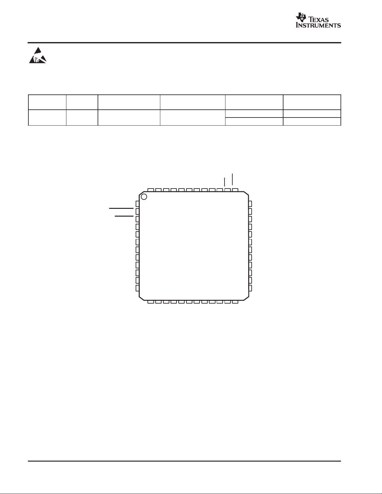
TLV320AIC28
QFN-48
RGZ
−40°C to +85°C
www.ti.com
SLAS418A − FEBRUARY 2004 − REVISED SEPTEMBER 2004
This integrated circuit can be damaged by ESD. Texas Instruments recommends that all integrated circuits be handled with appropriate
precautions. Failure to observe proper handling and installation procedures can cause damage.
ESD damage can range from subtle performance degradation to complete device failure. Precision integrated circuits may be more susceptible to
damage because very small parametric changes could cause the device not to meet its published specifications.
PACKAGE/ORDERING INFORMATION
PRODUCT PACKAGE
PIN ASSIGNMENTS
PACKAGE
DESIGNATOR
IOVDD
PWR_DN
RESET
GPIO2
GPIO1
AVDD2
AVSS2
AVDD1
NC
NC
NC
NC
DVSS
48 47 46 45 44 43 42 41 40 39 38 37
1
2
3
4
5
6
7
8
9
10
11
12
13
14 15 16 17 18 19 20 21 22 23 24
OPERATING
TEMPERATURE RANGE
QFN PACKAGE
(TOP VIEW)
DVDD
BCLK
WCLK
SDIN
SDOUT
MCLK
SCLK
ORDERING NUMBER TRANSPORT MEDIA
TLV320AIC28IRGZ Rails, 52
TLV320AIC28IRGZR Tape and Reel, 2500
MISO
MOSISSDAV
36
DRVSS2
35
OUT8P
34
BVDD
33
OUT8N
32
DRVSS1
31
VGND
30
SPKFC
29
DRVDD
28
SPK2
27
SPK1
26
OUT32N
25
MIC_DETECT_IN
2
VREF
AVSS1
VBAT
AUX2
AUX1
CP_IN
CP_OUT
BUZZ_IN
MICIN_HED
MICIN_HND
MICBIAS_HED
MICBIAS_HND
QFN package
www.ti.com
SLAS418A − FEBRUARY 2004 − REVISED SEPTEMBER 2004
Terminal Functions
PIN NAME DESCRIPTION PIN NAME DESCRIPTION
1 IOVDD IO Supply 25 MIC_DETECT_IN Microphone detect input
2 PWR_DN Hardware power down 26 OUT32N Receiver driver output
3 RESET Hardware reset 27 SPK1 Headset driver output/receiver driver output
4 GPIO2 General purpose IO 28 SPK2 Headset driver output
5 GPIO1 General purpose IO 29 DRVDD Headphone driver power supply
6 AVDD2 PLL analog power supply 30 SPKFC Driver feedback/ speaker detect input
7 AVSS2 Analog ground 31 VGND Virtual ground for audio output
8 AVDD1 Audio ADC, DAC, reference, SAR
ADC analog power supply
9 NC No connect 33 OUT8N Loudspeaker driver output
10 NC No connect 34 BVDD Battery power supply
11 NC No connect 35 OUT8P Loudspeaker driver output
12 NC No connect 36 DRVSS2 Driver ground
13 AVSS1 Analog ground 37 DAV Auxiliary data available output
14 VREF Reference voltage for SAR ADC 38 SS SPI Slave select input
15 VBAT Battery monitor input 39 MOSI SPI Serial data input
16 AUX2 Secondary auxiliary input 40 MISO SPI Serial data output
17 AUX1 First auxiliary input 41 SCLK SPI Serial clock input
18 BUZZ_IN Buzzer input 42 MCLK Master clock
19 CP_OUT Output to cell phone module 43 SDOUT Audio data output
20 CP_IN Input from cell phone module 44 SDIN Audio data input
21 MICIN_HND Handset microphone input 45 WCLK Audio word clock
22 MICBIAS_HND Handset microphone bias voltage 46 BCLK Audio bit clock
23 MICIN_HED Headset microphone input 47 DVDD Digital core supply
24 MICBIAS_HED Headset microphone bias voltage 48 DVSS Digital core and IO ground
32 DRVSS1 Driver ground
ABSOLUTE MAXIMUM RATINGS
over operating free-air temperature range unless otherwise noted
AVDD1/2 to AVSS1/2 −0.3 V to 3.9 V
DRVDD to DRVSS1/2 −0.3 V to 3.9 V
BVDD to DRVSS1/2 −0.3 V to 4.5 V
IOVDD to DVSS −0.3 V to 3.9 V
Digital input voltage to DVSS −0.3 V to IOVDD + 0.3 V
Analog input (except VBAT) voltage to AVSS1/2 −0.3 V to AVDD + 0.3 V
VBAT input voltage to AVSS1/2 −0.3 V to 6 V
AVSS1/2 to DR VSS1/2 to DVSS −0.1 V to 0.1 V
AVDD1/2 to DR VDD −0.1 V to 0.1 V
Operating temperature range −40°C to 85°C
Storage temperature range −65°C to 105°C
Junction temperature (TJ Max) 105°C
Power dissipation (TJ Max − TA)/θ
θ
Thermal impedance (with thermal pad soldered to board) 27°C/W
JA
Lead temperature Infrared (15 sec) 240°C
(1)
Stresses beyond those listed under “absolute maximum ratings” may cause permanent damage to the device. These are stress ratings only , a nd
functional operation of the device at these or any other conditions beyond those indicated under “recommended operating conditions” is not
implied. Exposure to absolute-maximum-rated conditions for extended periods may affect device reliability.
(2)
If the AIC28 is used to drive high power levels to an 8-Ω load for extended intervals at an ambient temperature above 80°C, multiple vias should
be used to electrically and thermally connect the thermal pad on the QFN package to an internal heat dissipating ground plane on the user’s PCB.
(1), (2)
UNITS
JA
3
V
Voltage range
www.ti.com
SLAS418A − FEBRUARY 2004 − REVISED SEPTEMBER 2004
ELECTRICAL CHARACTERISTICS
At +25°C, AVDD1, AVDD2, DRVDD, IOVDD = 3.3 V, BVDD = 3.9 V, DVDD = 1.8 V, V
PARAMETER TEST CONDITIONS MIN TYP MAX UNITS
BATTERY MONITOR INPUTS
Input voltage range 0.5 6.0 V
Input leakage current Battery conversion not selected ±1 µA
Variation across temperature after system
Accuracy
AUXILIARY A/D CONVERTER
Resolution Programmable: 8-, 10-,12-bits 8 12 Bits
No missing codes 12-Bit resolution 11 Bits
Integral nonlinearity −5 5 LSB
Offset error −6 6 LSB
Gain error −6 6 LSB
Noise 50 µVrms
VOLTAGE REFERENCE (VREF)
Voltage range
Reference drift Internal VREF = 1.25 V 50 ppm/°C
Current drain
AUDIO CODEC
ADC DECIMATION FILTER CHARACTERISTICS
Filter gain from 0 to 0.39 Fs ±0.1 dB
Filter gain at 0.4125 Fs −0.25 dB
Filter gain at 0.45 Fs −3.0 dB
Filter gain at 0.5 Fs −17.5 dB
Filter gain from 0.55 Fs to 64 Fs −75 dB
Group delay 17/Fs sec
calibration at 4 V battery voltage and room
temperature
VREF output programmed = 2.5 V 2.3 2.5 2.7
VREF output programmed = 1.25 V 1.25
External reference 1.1 2.5 V
Extra current drawn when the internal reference is
turned on.
= 2.5 V , Fs (Audio) = 48 kHz, unless otherwise noted
ref
±15 mV
750 µA
4
PSRR
Input resistance
Voltage range
V
PSRR
dB
Voltage range
V
PSRR
dB
www.ti.com
SLAS418A − FEBRUARY 2004 − REVISED SEPTEMBER 2004
ELECTRICAL CHARACTERISTICS (continued)
At +25°C, AVDD1, AVDD2, DRVDD, IOVDD = 3.3 V, BVDD = 3.9 V, DVDD = 1.8 V, Int. V
noted (continued)
PARAMETER TEST CONDITIONS MIN TYP MAX UNITS
MICROPHONE INPUT TO ADC
Full-scale input voltage (0 dB) 0.707 Vrms
Input common mode 1.5 V
SNR
THD 0.63 Vrms input, 0-dB gain −81 −72 dB
Mute attenuation
Input capacitance 10 pF
HEADSET MICROPHONE BIAS
Voltage range
Sourcing current Voltage drop <25 mV 5 mA
HANDSET MICROPHONE BIAS
Sourcing current Voltage drop <25 mV 5 mA
DAC INTERPOLATION FILTER
Pass band 20 0.45Fs Hz
Pass band ripple ±0.06 dB
Transition band 0.45Fs 0.5501Fs Hz
Stop band 0.5501Fs 7.455Fs Hz
Stop band attenuation 65 dB
Filter group delay 21/Fs Sec
De-emphasis error ±0.1 dB
(1)
ADC PSRR measurement is calculated as:
MICIN_HED 1020 Hz sine wave input,
Fs = 48 ksps
Measured as idle channel noise, 0 dB gain,
A-weighted
217 Hz, 100 mV on AVDD1/2
1020 Hz, 1 0 0 m V o n AVDD1/2
Output code with 0.63 Vrms sine wave input at
1 kHz
Only ADC on 15 50 kΩ
ADC and Sidetone on 8 16 kΩ
Register 1DH/Page 2, D7−D8=00 3.3
Register 1DH/Page 2, D7−D8=01 2.5
Register 1DH/Page 2, D7−D8=1X 2
217 Hz, 100 mV on AVDD1/2 55
217 Hz, 100 mV on BVDD 74
1020 Hz, 1 0 0 m V o n AVDD1/2 55
1020 Hz, 100 mV on BVDD 74
Register 1DH/Page 2, D6=0 2.5
Register 1DH/Page 2, D6=1 2
217 Hz, 100 mV on AVDD1/2 55
1020 Hz, 1 0 0 m V o n AVDD1/2 55
(1)
(1)
= 2.5 V, Fs (Audio) = 48 kHz, unless otherwise
ref
80 90 dBA
55 dB
55 dB
0000H
V
PSRR + 20 log
where VSIG
VSIG
sup
ǒ
10
V
ADCOUT
is the ac signal applied on AVDD1/2, which is 100 mVPP at 1020 Hz, and
sup
Ǔ
V
ADCOUT
Amplitude of Digital Output
+
Max Possible Digital Amplitude
5
PSRR
PSRR
dB
www.ti.com
SLAS418A − FEBRUARY 2004 − REVISED SEPTEMBER 2004
ELECTRICAL CHARACTERISTICS (continued)
At +25°C, AVDD1, AVDD2, DRVDD, IOVDD = 3.3 V, BVDD = 3.9 V, DVDD = 1.8 V, V
(continued)
PARAMETER TEST CONDITIONS MIN TYP MAX UNITS
DAC HEADPHONE OUTPUT Load = 16 Ω (single-ended), 50 pF
Full-scale output voltage (0dB) 0.848 Vrms
Output common mode 1.5 V
SNR Measured as idle channel noise, A-weighted 85 95 dBA
THD −1 dBFS Input, 0-dB gain −80 −60 dB
217 Hz, 100 mV on
AVDD1/AVDD2/DRVDD
1020 Hz, 100 mV on
AVDD1/AVDD2/DRVDD
Interchannel isolation Coupling from ADC to DAC 80 dB
Mute attenuation 100 dB
Maximum output power Per channel 44 mW
Digital volume control −63.5 0 dB
Digital volume control step size 0.5 dB
Channel separation Between SPK1 and SPK2 −75 dB
DAC SPEAKER OUTPUT Load = 8 Ω (differential), 50 pF
Full-scale output voltage (0 dB) 1.838 Vrms
Output common mode 1.75 V
SNR Measured as idle channel noise, A-weighted 90 98 dBA
THD −1 dBFS Input, 0-dB gain −74 −55 dB
217 Hz, 100 mV on AVDD1/2 70
217 Hz, 100 mV on BVDD 70
1020 Hz, 1 0 0 m V o n AVDD1/2 70
1020 Hz, 100 mV on BVDD 70
Interchannel isolation Coupling from ADC to DAC 90 dB
Mute attenuation 100 dB
Maximum output power 400 mW
CELLPHONE
MIC INPUT TO CPOUT
Full-scale input voltage (0 dB) 0.707 Vrms
Input common mode 1.5 V
Full-scale output voltage (0 dB) 0.707 Vrms
Output common mode 1.5 V
SNR Measured as idle channel noise, A-weighted 80 89 dBA
THD 0 dBFS Input, 0-dB gain −73 −60 dB
PSRR
Interchannel isolation CP_IN to CP_OUT 75 dB
Mute attenuation CP_OUT muted 100 dB
(1)
DAC PSRR measurement is calculated as:
1020-Hz Sine wave input on MICIN_HND,
load on CP_OUT = 10 kΩ, 50 pF
217 Hz, 100 mV on AVDD1/AVDD2/DRVDD 43
1020 Hz, 100 mV on
AVDD1/AVDD2/DRVDD
(1)
(1)
= 2.5 V , Fs (Audio) = 48 kHz, unless otherwise noted
ref
55 dB
55 dB
43
dB
VSIG
PSRR + 20 log
6
10
ǒ
V
sup
SPK1ń2
Ǔ
www.ti.com
SLAS418A − FEBRUARY 2004 − REVISED SEPTEMBER 2004
ELECTRICAL CHARACTERISTICS (continued)
At +25°C, AVDD1, AVDD2, DRVDD, IOVDD = 3.3 V, BVDD = 3.9 V, DVDD = 1.8 V, V
(continued)
PARAMETER TEST CONDITIONS MIN TYP MAX UNITS
CP_IN TO 32Ω RECEIVER (SPK1−OUT32N)
Full-scale input voltage (0 dB) 0.707 Vrms
Input common mode 1.5 V
Full-scale output voltage (0 dB) 1.697 Vrms
Output common mode 1.5 V
SNR Measured as idle channel noise, A-weighted 85 97 dBA
THD 0 dBFs input, 0 dB gain −77 −60 dB
PSRR
Interchannel isolation MICIN to RECEIVER 75 dB
Mute attenuation 100 dB
Maximum output power 82 mW
DIGIT AL INPUT/OUTPUT
Logic family CMOS
Logic level: V
Capacitive load 10 pF
IH
V
IL
V
OH
V
OL
1020-Hz Sine wave input on CP_IN, Load on
SPK1−OUT32N = 32 Ω (differential), 50 pF
217 Hz, 100 mV on AVDD1/AVDD2/DRVDD 43
1020 Hz, 100 mV on
AVDD1/AVDD2/DRVDD
IIH = +5 µA 0.7IOVDD V
IIL = +5 µA −0.3 0.3IOVDD V
IOH = 2 TTL loads 0.8IOVDD V
IOL = 2 TTL loads 0.1IOVDD V
= 2.5 V , Fs (Audio) = 48 kHz, unless otherwise noted
ref
43
dB
7
IOVDD
Analog supply current – audio play back only
mA
(1)
Analog supply current − mic record only
(1)
(2)
Total current
µA
Default current
(3)
A
www.ti.com
SLAS418A − FEBRUARY 2004 − REVISED SEPTEMBER 2004
ELECTRICAL CHARACTERISTICS (continued)
At +25°C, AVDD1, AVDD2, DRVDD, IOVDD = 3.3 V, BVDD = 3.9 V, DVDD = 1.8 V, V
(continued)
PARAMETER TEST CONDITIONS MIN TYP MAX UNITS
POWER SUPPLY REQUIREMENTS
Power supply voltage
AVDD1, AVDD2 3 3.3 3.6 V
DRVDD 3 3.3 3.6 V
BVDD 3 4.2 V
IOVDD Max MCLK = 100 MHz 2 3.6 V
Max MCLK = 50 MHz 1.1 3.6 V
DVDD 1.65 1.8 1.95 V
IAVDD1 with loudspeaker output (no signal),
PLL off
IBVDD with loudspeaker output (no signal),
PLL off
IAVDD1 with headphone output (no signal),
VGND off, PLL off
IDRVDD with headphone output (no signal),
VGND off, PLL off
Digital supply current – audio play back only IDVDD, PLL off 2.5 mA
IAVDD1, headset mic, PLL of f 5.2 mA
Analog supply current − mic record only
Digital supply current – mic record only IDVDD, PLL off 1.4 mA
Analog supply current IAVDD2, PLL on 1.3 mA
Digital supply current IDVDD, PLL on 0.9 mA
Total current
(1)
Mic record currents measured with no load on MICBIAS.
(2)
Current measured with MICBIAS_HED voltage programmed to 2 V (Page 2, Register 1DH, BIt D8=1).
(3)
Default currents measured with device in default mode after reset.
IBVDD, headset mic, PLL off 270 µA
IAVDD1, handset mic, PLL of f 5.6 mA
Hardware power down 27
Only headset/button detection enabled 50
Only auto temperature measurement with
5.59 min delay
Headset/button detection and auto
temperature measurement with 5.59 min
delay
IAVDD1 + IAVDD2 66
IBVDD 9
= 2.5 V , Fs (Audio) = 48 kHz, unless otherwise noted
ref
3.1
7.5
2.5
3.5
50
65
µA
µ
8
www.ti.com
FUNCTIONAL BLOCK DIAGRAM
SLAS418A − FEBRUARY 2004 − REVISED SEPTEMBER 2004
AVDD1 AVDD2 DRVDD BVDD DVDD IOVDD
VBAT
VREF
MICBIAS_HED
MIC_DETECT_IN
MICBIAS_HND
AUX1
AUX2
MICIN_HED
MICIN_HND
CP_IN
BUZZ_IN
OUT8P
OUT8N
OUT32N
SPK1
Temperature
Measurement
2.0/2.5/3.3
To Detection
block
2.0/2.5
−1
Battery
Monitor
12 to −34.5dB
(0.5dB steps)
0 to −45dB
(3dB steps)
12 to −34.5dB
(0.5dB steps)
−1
0 to 59.5dB
(0.5dB steps)
Sidetone
Σ
Σ
SAR
ADC
0 to 59.5dB
(0.5dB steps)
Internal
Reference
AGC
Σ
To ADC and DAC
Σ−∆
DAC
Σ−∆
ADC
PLL
Headset
detect and
Button
detect
0 to −63.5dB
(0.5dB steps)
OSC
Vol Ctl
SPI
Interface
Digital
Audio
Processing
and Serial
Interface
SCLK
SS
MOSI
MISO
DAV
RESET
MCLK
PWR_DN
SDOUT
WCLK
SDIN
BCLK
SPK2
CP_OUT
SPKFC
VGND
1.5V
Σ
Σ
To Detection block
AVSS2 DRVSS1 DRVSS2 DVSSAVSS1
Σ−∆
DAC
0 to −63.5dB
(0.5dB steps)
Vol Ctl
GPIO
Interface
GPIO1
GPIO2
9
PARAMETER
UNITS
SLAS418A − FEBRUARY 2004 − REVISED SEPTEMBER 2004
SPI TIMING DIAGRAM
www.ti.com
/SS
S
SPISELZ
S
S
SCLK
S
S
SPISELZ
S
SPICLK
MISO
S
E
SPISELZ
L
MOSI
SPISELZ
t
Lead
t
a
t
sck
t
t
t
wsck
t
t
su
MSB IN BIT6...1 LSB IN
wsck
v
MSBOUT BIT6...1 LSBOUT
t
hi
f
t
ho
TYPICAL TIMING REQUIREMENTS
All specifications typical at 25°C, DVDD = 1.8 V(1)
t
t
t
t
t
t
t
t
t
t
t
t
(1)
wsck
Lead
Lag
td
a
dis
su
hi
ho
v
r
f
SCLK Pulse width 30 18 ns
Enable Lead Time 18 15 ns
Enable Lag Time 18 15 ns
Sequential Transfer Delay 18 15 ns
Slave MISO access time 18 15 ns
Slave MISO disable time 18 15 ns
MOSI data setup time 6 6 ns
MOSI data hold time 6 6 ns
MISO data hold time 4 4 ns
MISO data valid time 25 13 ns
Rise Time 6 4 ns
Fall Time 6 4 ns
These parameters are based on characterization and are not tested in production.
t
t
Lag
t
r
IOVDD = 1.1 V IOVDD = 3.3 V
td
t
dis
MIN MAX MIN MAX
10
PARAMETER
(1)
UNITS
PARAMETER
(1)
UNITS
www.ti.com
SLAS418A − FEBRUARY 2004 − REVISED SEPTEMBER 2004
AUDIO INTERFACE TIMING DIAGRAMS
WCLK
(WS)
td
BCLK
SDOUT
SDIN
(DO−WS)
td
Figure 1. DSP Timing in Master Mode
Typical Timing Requirements (see Figure 1)
td(WS) WCLK delay 30 15 ns
td(DO−WS) WCLK to DOUT delay (for LJF mode) 30 15 ns
td(DO−BCLK) BCLK to DOUT delay 30 15 ns
ts(DI) SDIN setup 6 6 ns
th(DI) SDIN hold 6 6 ns
t
r
t
f
(1)
These parameters are based on characterization and are not tested in production.
Rise time 18 6 ns
Fall time 18 6 ns
(DO−BCLK)
td
(DI)
(DI)
ts
IOVDD = 1.1 V IOVDD = 3.3 V
MIN MAX MIN MAX
th
WCLK
BCLK
SDOUT
SDIN
(WS)
td
td
(WS)
(DO−BCLK)
td
(DI)
ts
(DI)
th
Figure 2. DSP Timing in Master Mode
Typical Timing Requirements (see Figure 2)
IOVDD = 1.1 V IOVDD = 3.3 V
MIN MAX MIN MAX
td(WS) WCLK delay 30 15 ns
td(DO−BCLK) BCLK to DOUT delay 30 15 ns
ts(DI) SDIN setup 6 6 ns
th(DI) SDIN hold 6 6 ns
t
r
t
f
(1)
These parameters are based on characterization and are not tested in production.
Rise time 18 6 ns
Fall time 18 6 ns
11
PARAMETER
(1)
UNITS
www.ti.com
SLAS418A − FEBRUARY 2004 − REVISED SEPTEMBER 2004
WCLK
(WS)
th
BCLK
SDOUT
SDIN
tL(BCLK)
tP(BCLK)
tH(BCLK)
Figure 3. I2S/LJF/RJF Timing in Slave Mode
Typical Timing Requirements (see Figure 3)
tH(BCLK) BCLK high period 40 35 ns
tL(BCLK) BCLK low period 40 35 ns
ts(WS) WCLK setup 6 6 ns
th(WS) WCLK hold 6 6 ns
td (DO−WS) WCLK to DOUT delay (for LJF mode) 30 18 ns
td(DO−BCLK) BCLK to DOUT delay 30 15 ns
ts(DI) SDIN setup 6 6 ns
th(DI) SDIN hold 6 6 ns
t
r
t
r
(1)
These parameters are based on characterization and are not tested in production.
Rise time 5 4 ns
Fall time 5 4 ns
(WS)
ts
(DO−WS)
td
(DO−BCLK)
td
(DI)
(DI)
ts
IOVDD = 1.1 V IOVDD = 3.3 V
MIN MAX MIN MAX
th
12
PARAMETER
(1)
UNITS
www.ti.com
SLAS418A − FEBRUARY 2004 − REVISED SEPTEMBER 2004
WCLK
(WS)
th
(WS)
ts
(DO−BCLK)
td
(DI)
(DI)
ts
IOVDD = 1.1 V IOVDD = 3.3 V
MIN MAX MIN MAX
th
BCLK
SDOUT
SDIN
tH(BCLK)
tP(BCLK)
(WS)
th
tL(BCLK)
(WS)
ts
Figure 4. DSP Timing in Slave Mode
Typical Timing Requirements (see Figure 4)
tH(BCLK) BCLK high period 40 35 ns
tL(BCLK) BCLK low period 40 35 ns
tP(BCLK) BCLK period 80 80 ns
ts(WS) WCLK setup 6 6 ns
th(WS) WCLK hold 6 6 ns
td(DO−BCLK) BCLK to DOUT delay 30 15 ns
ts(DI) SDIN setup 6 6 ns
th(DI) SDIN hold 6 6 ns
t
r
t
f
(1)
These parameters are based on characterization and are not tested in production.
Rise time 5 4 ns
Fall time 5 4 ns
13
SLAS418A − FEBRUARY 2004 − REVISED SEPTEMBER 2004
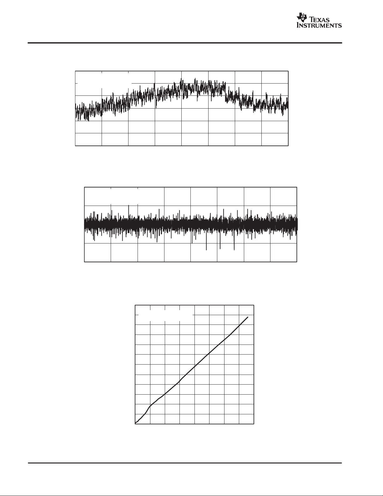
TYPICAL CHARACTERISTICS
1.5
AV
/AV
DD2
= 3.3 V ,
LSB
0.5
−0.5
−1
TA = 25C,
1
IR = 2.5 V
0
DD1
www.ti.com
−1.5
0
500 1000 1500 2000 2500 3000 3500 4000
CODE
Figure 5. SAR INL (TA = 25C, Internal Reference = 2.5 V, 12 bit, AVDD1/AVDD2 = 3.3 V)
1
AV
/AV
= 3.3 V ,
DD2
500 1000 1500 2000 2500 3000 3500 4000
CODE
LSB
−0.5
0.5
−1
0
0
DD1
TA = 25C,
IR = 2.5 V
Figure 6. SAR DNL (TA = 25C, Internal Reference = 2.5 V, 12 bit, AVDD1/AVDD2 = 3.3 V)
2.4
AV
/AV
2.2
1.8
1.6
1.4
1.2
DD1
TA = 25C
2
DD2
= 3.3 V ,
1
Power − mW
0.8
0.6
0.4
0.2
0
10 20 30 40 50 60 70 80
0
Sampling Rate − Ksps
Figure 7. SAR ADC Power Consumption vs Speed (TA = 25C, External Reference, AUX Conversion,
AVDD1/AVDD2 = 3.3 V)
14
www.ti.com
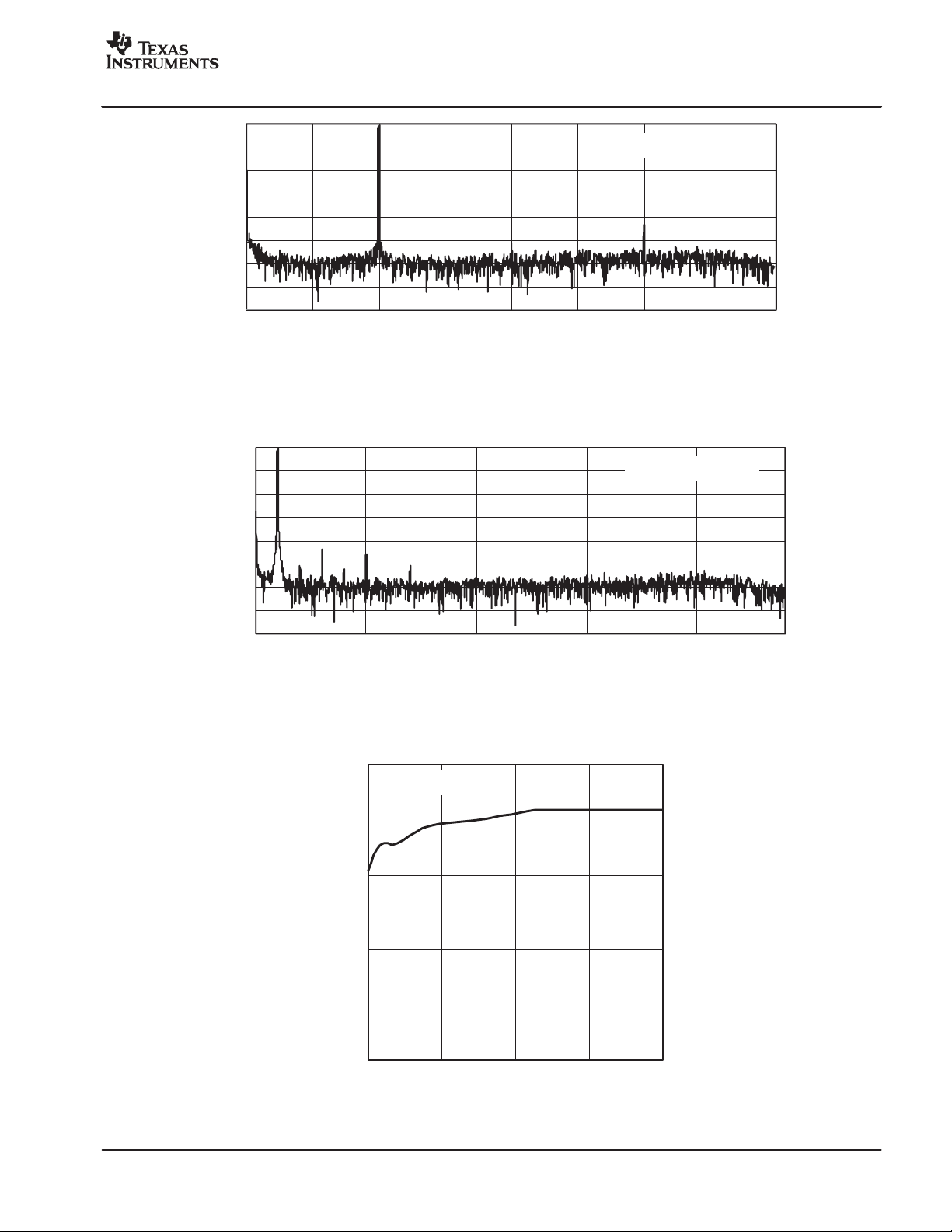
SLAS418A − FEBRUARY 2004 − REVISED SEPTEMBER 2004
dB
−20
−40
−60
−80
−100
−120
−140
−160
0
0
500 1000 1500 2000 2500 3000 3500 4000
f − Frequency − Hz
AV
/AV
DD1
TA = 25C,
DD2
= 3.3 V ,
Figure 8. ADC FFT Plot at 8 ksps (TA = 25C, −1 dB, 1 kHz input, AVDD1/AVDD2 = 3.3 V)
dB
−20
−40
−60
−80
−100
−120
−140
−160
0
0
5000 10000 15000 20000
f − Frequency − Hz
AV
/AV
DD1
TA = 25C,
DD2
= 3.3 V ,
Figure 9. ADC FFT Plot at 48 ksps (TA = 25C, −1 dB, 1 kHz input, AVDD1/AVDD2 = 3.3 V)
90
AV
/AV
DD1
TA = 25C,
89.5
89
88.5
88
87.5
Dynamic Range − dB
87
86.5
86
8 18283848
= 3.3 V ,
DD2
Sampling Rate − Ksps
Figure 10. ADC Dynamic Range vs Sampling Rate (TA = 25C, AVDD1/AVDD2 = 3.3 V)
15
SLAS418A − FEBRUARY 2004 − REVISED SEPTEMBER 2004
www.ti.com
dB
20
0
−20
−40
−60
−80
−100
−120
−140
−160
AV
/AV
DD2
= 3.3 V ,
f − Frequency − Hz
DD1
TA = 25C,
RL = 16
0 5000 10000 15000 20000
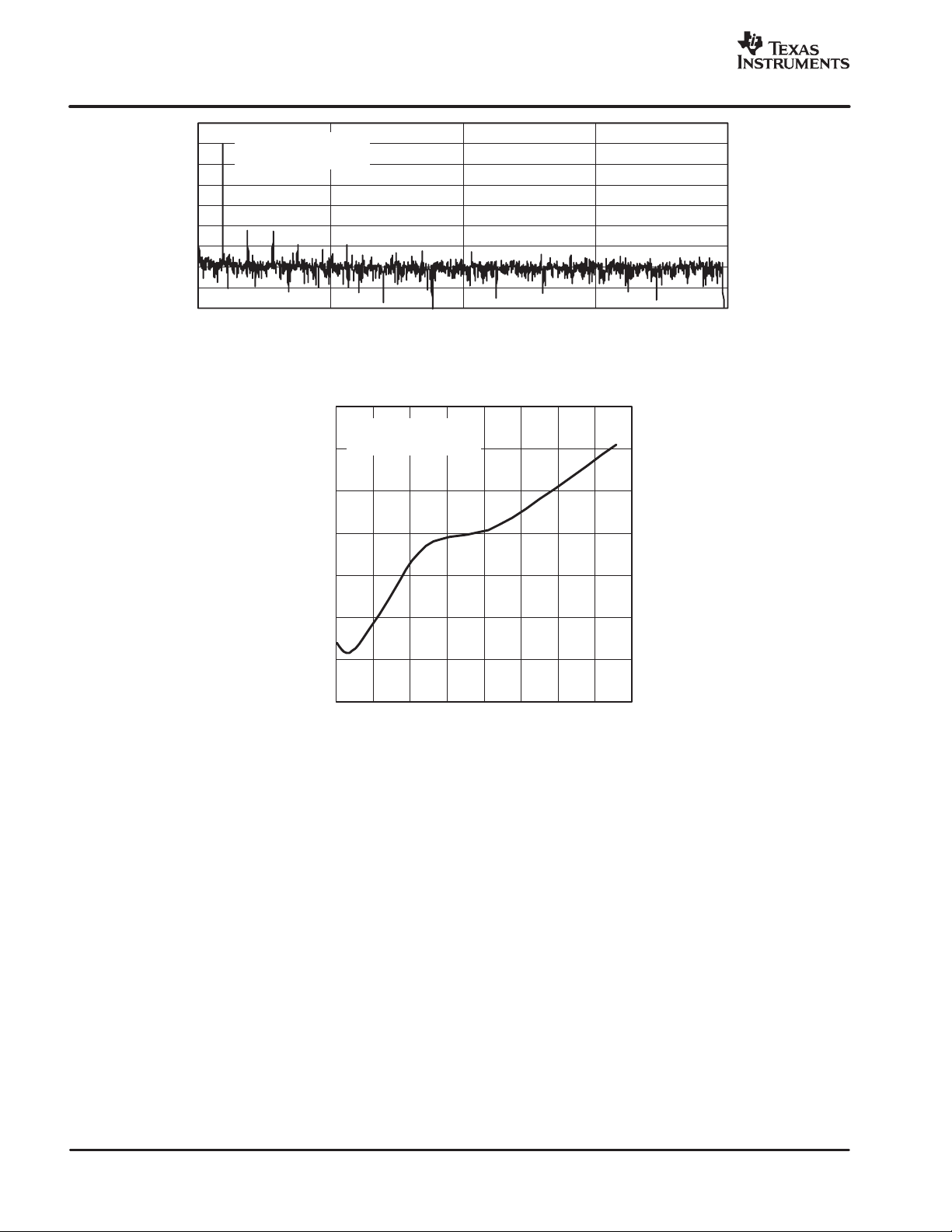
Figure 11. DAC FFT Plot (TA = 25C, −1 dB, 1 kHz Input, AVDD1/AVDD2/DRVDD = 3.3 V, R
−77
AV
/AV
DD2
= 3.3 V ,
−78
−79
−80
−81
DD1
TA = 25C,
RL = 16
= 16 Ω)
L
−82
−83
THD − Total Hormonic Distortion − dB
−84
5 1015202530354045
Power − mW
Figure 12. THD vs Power on SPK1/2 (TA = 25C, 1 kHz Input, AVDD1/AVDD2/DRVDD = 3.3 V, R
= 16 Ω)
L
16
www.ti.com
SLAS418A − FEBRUARY 2004 − REVISED SEPTEMBER 2004
−60
AV
/AV
DD1
BVDD = 3.9 V
TA = 25C,
−65
RL = 8
−70
−75
−80
−85
THD − Total Hormonic Distortion − dB
−90
0 50 100 150 200 250 300 350 400
Figure 13. THD vs Power on Loudspeaker Driver (TA = 25C, 1 kHz Input, AVDD1/AVDD2/DRVDD = 3.3 V,
BVDD = 3.9 V, R
/DRDD = 3.3 V ,
DD2
Power − mW
= 8 Ω)
L
450
400
350
300
250
Max Power Output − mW
200
150
2.7 2.9 3.1 3.3 3.5 3.7 3.9 4.1
BVDD − V
Figure 14. Loudspeaker Driver Output Power vs BVDD (TA = 25C, 1 kHz Input,
AVDD1/AVDD2/DRVDD = 3.3 V, R
= 8 Ω, THD v −40 dB)
L
17

SLAS418A − FEBRUARY 2004 − REVISED SEPTEMBER 2004
OVERVIEW
The AIC28 is a highly integrated stereo audio DAC and mono audio ADC for portable computing,
communication and entertainment applications. The AIC28 has a register-based architecture where all
peripheral functions are controlled through the registers and on-board state machines.
The AIC28 consists of the following blocks:
D Audio Codec
D Headset and Button Detection
D Battery Monitors
D Auxiliary Inputs
D Temperature Monitor
Communication to the AIC28 is via a standard SPI serial interface. This interface requires that the Slave Select
signal (SS) be driven low to communicate with the AIC28. Data is then shifted into or out of the AIC28 under
control of the host microprocessor, which also provides the serial data clock.
Control of the AIC28 and its functions is accomplished by writing to different registers in the AIC28. A simple
command protocol is used to address the 16-bit registers. Registers control the operation of the SAR ADC and
audio codec.
www.ti.com
OPERATION—AUDIO CODEC
AUDIO ANALOG I/O
The AIC28 has stereo audio DAC and mono audio ADC. It has a wide range of analog interfaces to support
different headsets and analog outputs. The AIC28 has features to interface output drivers (8-Ω, 16-Ω, 32-Ω)
and Microphone PGA to Cell-phone. The AIC28 also has a virtual ground (VGND) output, which can be
optionally used to connect to the ground terminal of a speaker of headphone to eliminate the ac-coupling
capacitor needed at the speaker or headphone output. A special circuit has also been included in the AIC28
to insert a short keyclick sound into the stereo audio output, even when the audio DAC is powered down. They
keyclick sound is used to provide feedback to the used when a particular button is pressed or item is selected.
The specific sound of the keyclick can be adjusted by varying several register bits that control its frequency,
duration, and amplitude.
AUDIO DIGITAL I/O INTERFACE
Digital audio data samples can be transmitted between the AIC28 and the CPU via the serial bus (BCLK, WCLK,
SDOUT, SDIN) that can be configured to transfer digital data in four different formats: Right justified (RJF), Left
justified (LJF), I2S and DSP. The four modes are MSB first and operate with variable word length between
16/20/24/32 bits. The AIC28’s audio codec can operate in master or slave mode, depending on its register
settings. The word-select signal (WCLK) and bit clock signal (BCLK) are configured as outputs when the bus
is in master mode. They are configured as inputs when the bus is in slave mode. The WCLK is representative
of the sampling rate of the audio ADC/DAC and is synchronized with SDOUT. Although the SDOUT signal can
contain two channels of information (a left and right channel), the AIC28 sends the same ADC data in both
channels.
D ADC/DAC Sampling Rate
The audio-control-1 register (Register 00H, Page 2) determines the sampling rates of DAC and ADC. The
sampling frequency is scaled down from the reference rate (Fsref). The reference rate is usually either 44.1
kHz or 48 kHz which can be selectable using bit D13 of the register Audio Control 3 (06H/Page2). The ADC
and DAC can operate with either common WCLK (equal sampling rates) or separate GPIO1 (For ADC) and
WCLK (For DAC) for unequal sampling rates. When the audio codec is powered up, it is by default configured
as an I2S slave with both the DAC and ADC operating at Fsref.
18
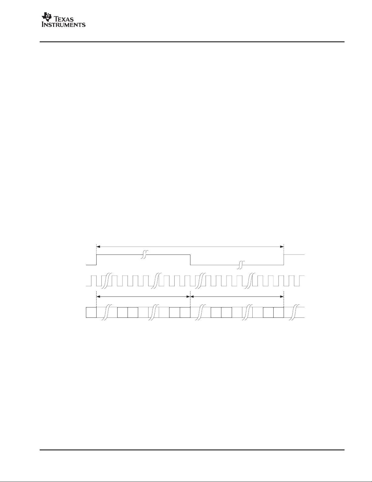
www.ti.com
SLAS418A − FEBRUARY 2004 − REVISED SEPTEMBER 2004
D Word Select Signals
The word select signal (WCLK) indicates the channel being transmitted:
2
— WCLK = 0: left channel for I
— WCLK = 1: right channel for I2S mode.
For other modes refer to the timing diagrams below.
D Bitclock (BCLK) Signal
In addition to being programmable as master or slave mode, the BCLK can also be configured in two transfer
modes, 256-S transfer mode and continuous transfer mode, which are described below. These modes are
set using bit D12 of control register 06H/page 2.
D 256-S Transfer Mode
In the 256-S mode, the BCLK rate always equals 256 times the WCLK frequency. In the 256-S mode, the
combination of ADC/DAC sampling rate equal to Fsref (as selected by bit D5D0 of control register 00H/page
2) and left-justified mode is not supported. If IOVDD is equal to 1.1 V, then ADC/DAC sampling rate should be
less than 39 kHz for all modes except the left justified mode where it should be less than 24 kHz.
D Continuous Transfer Mode
In the continuous transfer mode, the BCLK rate always equals two-word length times the frequency of
WCLK.
S mode;
D Right Justified Mode
In right-justified mode, the LSB of left channel is valid on the rising edge of BCLK preceding, the falling edge
on WCLK. Similarly the LSB of right channel is valid on the rising edge of BCLK preceding the rising edge of
WCLK.
1/fs
WCLK
BCLK
Left Channel Right Channel
SDIN/
SDOUT
n n−1 1 00 n n−1 1 0
n−2 2 2n−2
LSBMSB
Figure 15. Timing Diagram for Right-Justified Mode
19
SLAS418A − FEBRUARY 2004 − REVISED SEPTEMBER 2004
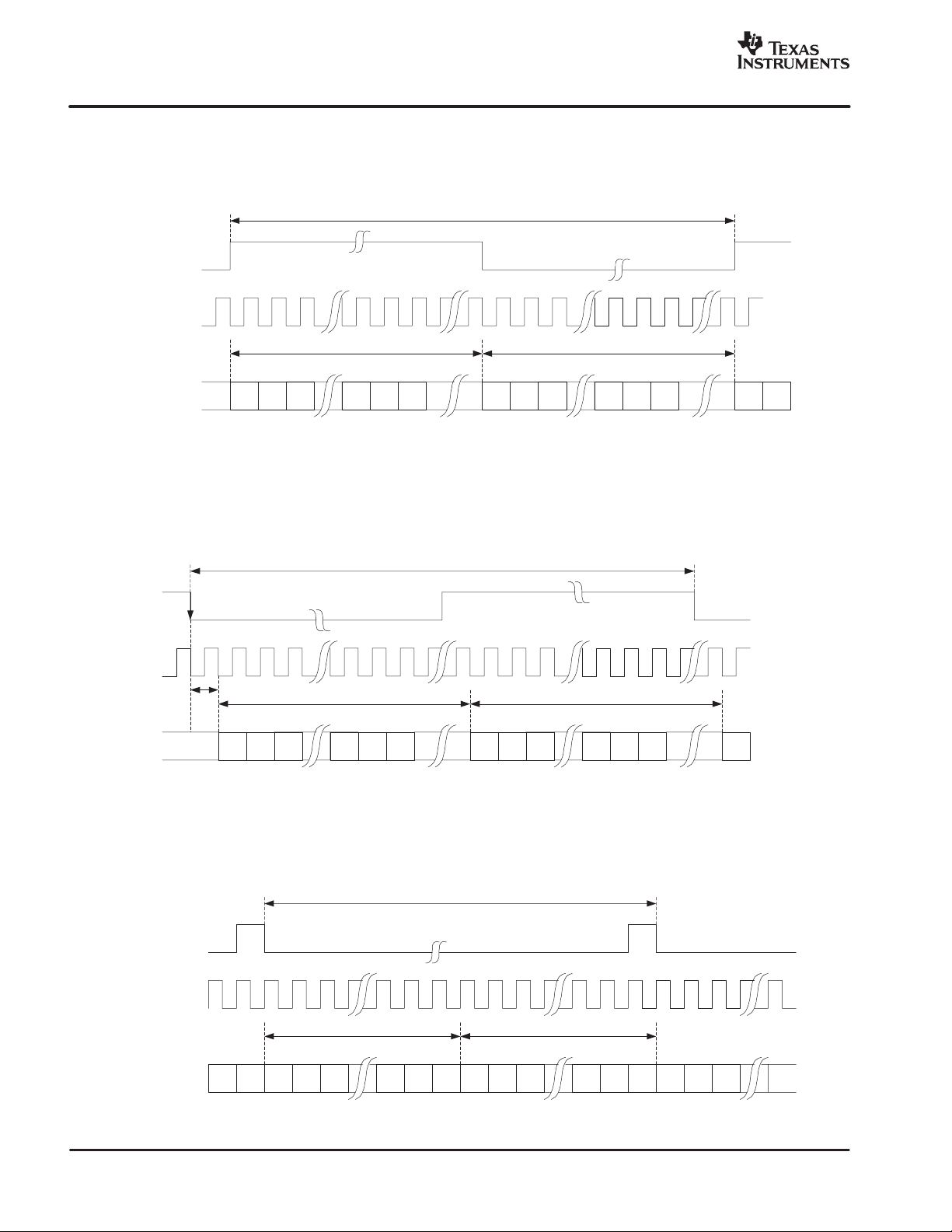
D Left Justified Mode
In left-justified mode, the MSB of right channel is valid on the rising edge of BCLK, following the falling edge on
WCLK. Similarly the MSB of left channel is valid on the rising edge of BCLK following the rising edge of
WCLK.
WCLK
BCLK
Left Channel Right Channel
SDIN/
SDOUT
2
D I
S Mode
In I2S mode, the MSB of left channel is valid on the second rising edge of BCLK, after the falling edge on
WCLK. Similarly the MSB of right channel is valid on the second rising edge of BCLK, after the rising edge of
WCLK.
n n−1 1 0 n n−1 1 0
Figure 16. Timing Diagram for Left-Justified Mode
www.ti.com
1/fs
n n−1n−2 2 n−2 2
LSBMSB
1/fs
WCLK
BCLK
1 clock before MSB
Left Channel Right Channel
SDIN/
SDOUT
n n−1 1 0 n n−1 1 0
n−2 2 n−2 2
LSBMSB
n
Figure 17. Timing Diagram for Right-Justified Mode
D DSP Mode
In DSP mode, the falling edge of WCLK starts the data transfer with the left channel data first and immediately
followed by the right channel data. Each data bit is valid on the falling edge of BCLK.
1/fs
WCLK
BCLK
Left Channel Right Channel
SDIN/
SDOUT
n n−1 1 0 n n−1 1 0
n−2 2 n−2 2 n−2
LSBMSB
MSB LSB
n n−11 0
MSBLSB
20
Figure 18. Timing Diagram for DSP Mode

www.ti.com
SLAS418A − FEBRUARY 2004 − REVISED SEPTEMBER 2004
AUDIO DATA CONVERTERS
The AIC28 includes a stereo audio DAC and a mono audio ADC. Both ADC and DAC can operate with a
maximum sampling rate of 53 kHz and support all audio standard rates of 8 kHz, 11.025 kHz, 12 kHz, 16 kHz,
22.05 kHz, 24 kHz, 32 kHz, 44.1 kHz, and 48 kHz. By utilizing the flexible clock generation capability and internal
programmable interpolation, a wide variety of sampling rates up to 53 kHz can be obtained from many possible
MCLK inputs. In addition, the DAC and ADC can independently operate at different sampling rates as indicated
in control register 00H/page 2.
When the ADC or DAC is operating, the AIC28 requires an applied audio MCLK input. The user should also
set bit D13 of control register 06H/page 2 to indicate which Fsref rate is being used. If the codec ADC or DAC
is powered up, then the auxiliary ADC uses MCLK and BCLK for its internal clocking, and the internal oscillator
is powered down to save power.
Typical audio DACs can suffer from poor out-of-band noise performance when operated at low sampling rates,
such as 8 kHz or 11.025 kHz. The AIC28 includes programmable interpolation circuitry to provide improved
audio performance at such low sampling rates, by first upsampling low-rate data to a higher rate, filtering to
reduce audible images, and then passing the data to the internal DAC, which is actually operating at the Fsref
rate. This programmable interpolation is determined using bit D5D3 of control register 00H/page 2.
For example, if playback of 11.025 kHz data is required, the AIC28 can be configured such that Fsref = 44.1
kHz. Then using bit D5D3 of control register/page 2, the DAC sampling rate (Fs) can be set to Fsref/4, or FS
= 11.025 kHz. In operation, the 11.025 kHz digital input data is received by the AIC28, upsampled to 44.1 kHz,
and filtered for images. It is then provided to the audio DAC operating at 44.1 kHz for playback. In reality, the
audio DAC further upsamples the 44.1 kHz data by a ratio of 128 x and performes extensive interpolation
filtering and processing on this data before conversion to a stereo analog output signal.
Phase Locked Loop (PLL)
The AIC28 has an on chip PLL to generate the needed internal ADC and DAC operational clocks from a wide
variety of clocks that may be available in the system. The PLL supports an MCLK varying from 2 MHz to 100
MHz and is register programmable to enable generation of required sampling rates with fine precision.
ADC and DAC sampling rates are given by
DAC_Fs +
Fsref
N1
and
ADC_Fs +
Fsref
N2
Where, Fsref must fall between 39 kHz and 53 kHz, and N1, N2=1, 1.5, 2, 3, 4, 5, 5.5, 6 are register
programmable.
The PLL can be enabled or disabled using register programming.
D When PLL is disabled
Fsref +
Q = 2, 3…17
— Note: For ADC, with N2 = 1.5 or 5.5, odd values of Q are not allowed.
— In this mode, the MCLK can operate up to 100 MHz, and Fsref should fall between 39 kHz
and 53 kHz.
MCLK
128 Q
D When PLL is enabled
21

SLAS418A − FEBRUARY 2004 − REVISED SEPTEMBER 2004
www.ti.com
Fsref +
P = 1, 2, 3 … 8
K = J.D
J = 1, 2, 3 ….64
D = 0, 1, 2 … 9999
P, J and D are register programmable.where J is integer part of K before the decimal point, and D
is four-digit fractional part of K after the decimal point, including lagging zeros.
MCLK K
2048 P
Examples: If K = 8.5, then J = 8, D = 5000
If K = 7.12, then J = 7, D = 1200
If K = 7.012, then J = 7, D = 120
The PLL is programmed through Registers 1BH and 1CH of Page 2.
D When PLL is enabled and D = 0, the following conditions must be satisfied
2MHzv
80 MHz v
MCLK
P
MCLK K
P
4Ă v J vĂ55
v 20 MHz
v 110 MHz
D When PLL is enabled D ≠ 0, the following conditions must be satisfied
10 MHz v
MCLK
P
v 20 MHz
80 MHz v
MCLK K
P
v 110 MHz
4Ă v J vĂ11
Example 1:
For MCLK = 12 MHz and Fsref = 44.1 kHz
P = 1, K = 7.5264
J = 7, D = 5264
Example 2:
For MCLK = 12 MHz and Fsref = 48 kHz
P = 1, K = 8.192
J = 8, D = 1920
MONO AUDIO ADC
Analog Front End
The analog front end of the audio ADC consists of an analog MUX and a programmable gain amplifier (PGA).
The MUX can connect either of the Headset Input (MICIN_HED), Handset Input (MICIN_HND), AUX1 and
AUX2 signal through the PGA to the ADC for audio recording. The Cell-phone Input (CP_IN) can also be
connected to ADC through a PGA at the same time. This enables recording of conversation during a cell-phone
call. The AIC28 also has an option of choosing MICIN_HED/MICIN_HND and AUX1/AUX2 as differential input
pair. The AIC28 also includes two microphone bias circuits which can source up to 5 mA of current, and are
programmable to a 2 V, 2.5 V or 3.3 V level for Headset and 2 V or 3.3 V level for handset.
Because of the oversampling nature of the audio ADC and the integrated digital decimation filtering,
requirements for analog anti-aliasing filtering are very relaxed. The AIC28 integrates a second order analog
anti-aliasing filter with 20-dB attenuation at 1 MHz. This filter, combined with the digital decimal filter, provides
sufficient anti-aliasing filtering without requiring any external components.
22

www.ti.com
SLAS418A − FEBRUARY 2004 − REVISED SEPTEMBER 2004
The PGA, for microphone and AUX Inputs, allows analog gain control from 0 dB to 59.5 dB in steps of 0.5 dB.
The PGA gain changes are implemented with an internal soft-stepping. This soft-stepping ensures that volume
control changes occur smoothly with no audible artifacts. Upon reset, the PGA gain defaults to a mute condition,
and upon power down, the PGA soft-steps the volume to mute before shutting down. A read-only flag (D0
control register 04H/Page 2) is set whenever the gain applied by PGA equals the desired value set by the
register. The soft-stepping control can be disabled by programming D15=1 in register 1DH of Page 2. When
soft stepping is enabled and ADC power down register is written, MCLK should be running to ensure that
soft-stepping to mute has completed. MCLK can be shut down once Mic PGA power down flag is set.
The PGA, for Cell phone Input (CP_IN) allows gain control from –34.5 dB to 12 dB in steps of 0.5 dB. The PGA
gain changes are implemented with an internal soft−stepping. This soft-stepping ensures that volume control
changes occur smoothly with no audible artifacts. Upon reset, the PGA gain defaults to a mute condition, and
upon power down, the PGA soft-steps the volume to mute before shutting down. A read−only flag (D7 control
register 1FH/Page 2) is set whenever the gain applied by PGA equals the desired value set by the register. The
soft-stepping control can be disabled by the programming D12=1 in register 1DH of Page 2. When soft-stepping
is enabled and ADC power down register is written, MCLK should be running to ensure that soft-stepping to
mute has completed. MCLK can be shut down once Cell PGA power down flag is set.
Delta-Sigma ADC
The analog-to-digital converter has a delta-sigma modulator with a 128 times oversampling ratio. The ADC can
support maximum output rate of 53 kHz.
Decimation Filter
The audio ADC includes an integrated digital decimation filter that removes high frequency content and
downsamples the audio data from an initial sampling rate of 128 times Fs to the final output sampling rate of
Fs. The decimation filter provides a linear phase output response with a group delay of 17/Fs. The –3 dB
bandwidth of the decimation filter extends to 0.45 Fs and scales with the sample rate (Fs).
Programmable High Pass Filter
The ADC channel has a programmable high-pass filter whose cutoff frequency can be programmed through
control register. By default the high pass filter is off. The high-pass filter is a first order IIR filter. This filter can
be used to remove the DC component of the input signal and offset of the ADC channel.
Automatic Gain Control (AGC)
The AIC28 includes Automatic gain control (AGC) for Microphone Inputs (MICIN_HED or MICIN_HND) and
Cell-phone input (CP_IN). AGC can be used to maintain nominally constant output signal amplitude when
recording speech signals. This circuitry automatically adjusts the PGA gain as the input signal becomes overly
loud or very weak, such as when a person speaking into a microphone moves closer or farther from the
microphone. The AGC algorithm has several programmable settings, including target gain, attack and decay
time constants, noise threshold, and max PGA applicable that allow the algorithm to be fine tuned for any
particular application. The algorithm uses the absolute average of the signal (which is the average of the
absolute value of the signal) as a measure of the nominal amplitude of the output signal.
Target gain represents the nominal output level at which the AGC attempts to hold the ADC output signal level.
The AIC28 allows programming of eight different target gains, which can be programmed from –5.5 dB to –24
dB relative to a full-scale signal. Since the AIC28 reacts to the signal absolute average and not to peak levels,
it is recommended that the target gain be set with enough margin to avoid clipping at the occurrence of loud
sounds.
Attack time determines how quickly the AGC circuitry reduces the PGA gain when the input signal is too loud.
It can be varied from 8 ms to 20 ms.
Decay time determines how quickly the PGA gain is increased when the input signal is too low. It can be varied
in the range from 100 ms to 500 ms.
Noise threshold is the minimum amplitude for the input signal that the AGC considers as a valid signal. If the
average amplitude of the incoming signal falls below this value, the AGC considers it as silence and brings down
the gain to 0 dB in steps of 0.5 dB for every FS. This will also set the noise threshold flag. The gain stays at
23
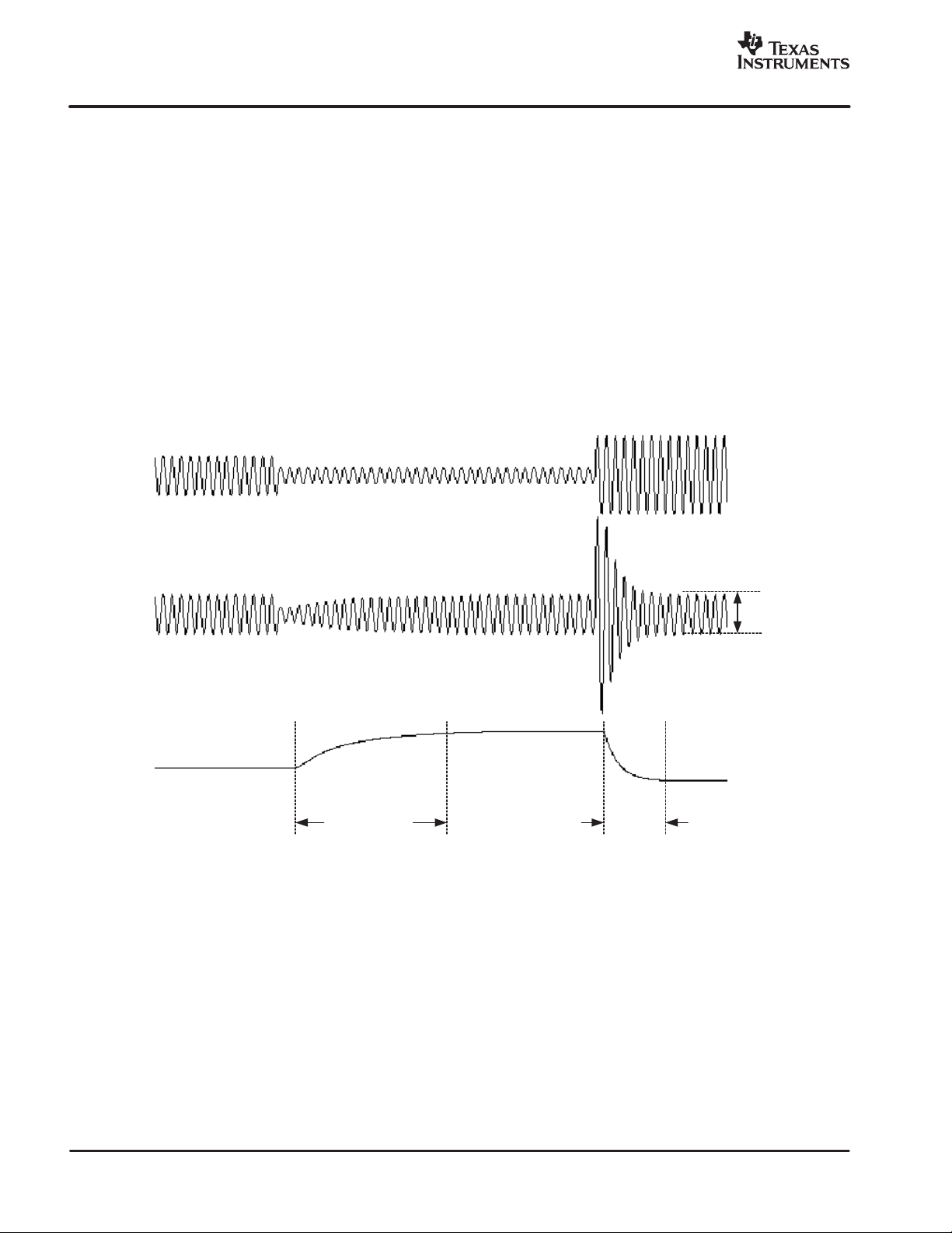
SLAS418A − FEBRUARY 2004 − REVISED SEPTEMBER 2004
0 dB until the average amplitude of the input signal rises above the noise threshold value. This ensures that
noise does not get amplified in the absence of a valid input speech signal. Noise threshold level is programmable
from −30dB to −90 dB for microphone input, and from −30 dB to −60 dB for cell-phone input. When AGC Noise
Threshold is set to −70 dB, −80 dB, or −90 dB, the microphone input Max PGA applicable setting must be greater
than or equal to 11.5 dB, 21.5 dB, or 31.5 dB respectively. This operation includes debounce and hysteresis
to avoid the AGC gain from cycling between high gain and 0 dB when the signal amplitude is near the noise
threshold level. When the noise threshold flag is set, status of gain applied by AGC and saturation flag should
be ignored.
Maximum input gain applicable allows user to restrict maximum gain applied by the AGC. This can be used
for limiting PGA gain in situations where environment noise is greater than programmed noise threshold.
Microphone input Max PGA can be programmed from 0 dB to 59.5 dB in steps of 0.5 dB. Cell-phone input Max
PGA can be programmed from −34.5 dB to −0.5 dB in steps of 0.5 dB, as well as +12 dB.
See Table 1 for various AGC programming options. AGC can be used only if microphone input or Cell-phone
input is routed to the ADC channel. When both microphone input and Cell-phone input are connected to the
ADC, AGC is automatically disabled.
Input
Signal
www.ti.com
Output
Signal
AGC
Gain
Decay Time
Figure 19. AGC Characteristics
Target
Gain
Attack
Time
24
www.ti.com
SLAS418A − FEBRUARY 2004 − REVISED SEPTEMBER 2004
Table 1. AGC Settings
MIC HEADSET INPUT MIC HANDSET INPUT CELL-PHONE INPUT
BIT
AGC enable D0 01H D0 1EH D0 24H
Target gain D7−D5 01H D7−D5 1EH D7−D5 24H
Time constants (attack and decay time) D4−D1 01H D4−D1 1EH D4−D1 24H
Noise threshold D13−D11 24H D13−D11 24H D13−D11 24H
Noise threshold flag D11 04H D11 04H D14 24H
Hysteresis D10−D9 1DH D10−D9 1DH D10−D9 24H
Debounce time (normal to silence mode) D8−D6 26H D8−D6 26H D8−D6 27H
Debounce time (silence to normal mode) D5−D3 26H D5−D3 26H D5−D3 27H
Max PGA applicable D15−D9 26H D15−D9 26H D15−D9 27H
Gain applied by AGC D15−D8 01H D15−D8 1EH D14−D8 1FH
Saturation flag D0 04H D0 04H D7 1FH
Clip stepping disable D3 06H D3 06H D8 24H
NOTE:All settings shown in Table 1 are located in Page 2 of control registers.
CONTROL
REGISTER
BIT
Stereo Audio DAC
CONTROL
REGISTER
BIT
CONTROL
REGISTER
Each channel of the stereo audio DAC consists of a digital audio processing block, a digital interpolation filter,
digital delta-sigma modulator, and an analog reconstruction filter. The DAC is designed to provide enhanced
performance at low sample rates through increased oversampling and image filtering, thereby keeping
quantization noise generated within the delta-sigma modulator and signal images strongly suppressed within
the audio band to beyond 20 kHz. This is realized by keeping the upsampled rate constant at 128 x Fsref and
changing the oversampling ratio as the input sample rate is changed. For Fsref of 48 kHz, the digital delta−sigma
modulator always operates at a rate of 6.144 MHz. This ensures that quantization noise generated within the
delta-sigma modulator stays within the frequency band below 20 kHz at all sample rates. Similarly, for Fsref
rate of 44.1 kHz, the digital delta-sigma modulator always operates at a rate of 5.6448 MHz.
Digital Audio Processing
The DAC channel consists of optional filters for de-emphasis and bass, treble, midrange level adjustment, or
speaker equalization. The de-emphasis function is only available for sample rates of 32 kHz, 44.1 kHz, and 48
kHz. The transfer function consists of a pole with time constant of 50ms and a zero with time constant of 15ms.
Frequency response plots are given in the Audio Codec Filter Frequency Responses section of this data sheet.
The DAC digital effects processing block consists of a fourth order digital IIR filter with programmable
coefficients (one set per channel). The filter is implemented as cascade of two biquad sections with frequency
response given by:
N0 ) 2 N1 z*1) N2 z
ǒ
32768 * 2 D1 z*1* D2 z
*2
N3 ) 2 N4 z*1) N5 z
Ǔǒ
*2
32768 * 2 D4 z*1* D5 z
*2
*2
Ǔ
The N and D coefficients are fully programmable, and the entire filter can be enabled or bypassed. The
coefficients for this filter implement a variety of sound effects, with bass-boost or treble boost being the most
commonly used in portable audio applications. The default N and D coefficients in the part are given by:
N0 = N3 = 27619
N1 = N4 = −27034
N2 = N5 = 26461
D1 = D4 = 32131
D2 = D5 = −31506
25

SLAS418A − FEBRUARY 2004 − REVISED SEPTEMBER 2004
These coefficients implement a shelving filter with 0 dB gain from dc to approximately 150 Hz, at which point
it rolls off to 3 dB attenuation for higher frequency signals, thus giving a 3-dB boost to signals below 150 Hz.
The N and D coefficients are represented by 16−bit twos complement numbers with values ranging from –32768
to +32767. Frequency response plots are given in the Audio Codec Filter Frequency Responses section of this
data sheet.
Interpolation Filter
The interpolation filter upsamples the output of the digital audio processing block by the required oversampling
ratio. It provides a linear phase output with a group delay of 21/Fs.
In addition, the digital interpolation filter provides enhanced image filtering to reduce signal images caused by
the upsampling process that are below 20 kHz. For example, upsampling an 8-kHz signal produces signal
images at multiples of 8 kHz, i.e., 8 kHz, 16 kHz, 24 kHz, etc. The images at 8 kHz and 16 kHz are below 20
kHz and still audible to the listener, therefore, they must be filtered heavily to maintain a good quality output.
The interpolation filter is designed to maintain at least 65 dB rejection of images that land below 7.455 Fs. In
order to utilize the programmable interpolation capability, the Fsref should be programmed to a higher rate
(restricted to be in the range of 39 kHz to 53 kHz when the PLL is in use), and the actual FS is set using the
dividers in bits D5D3 of control register 00H/page 2. For example, if Fs = 8 kHz is required, then Fsref can be
set to 48 kHz, and the DAC Fs set to Fsref/6. This ensures that all images of the 8-kHz data are sufficiently
attenuated well beyond a 20-kHz audible frequency range. Passband ripple for all sample-rate cases (from 20
Hz to 0.45 Fs) is +0.06 dB maximum.
www.ti.com
Delta-Sigma DAC
The audio digital-to-analog converter incorporates a third order multi-bit delta-sigma modulator followed by an
analog reconstruction filter. The DAC provides high-resolution, low−noise performance, using oversampling
and noise shaping techniques. The analog reconstruction filter design consists of a 6 tap analog FIR filter
followed by a continuous time RC filter. The analog FIR operates at 6.144 MHz (128x48 kHz, for Fsref of 48
kHz) or at 5.6448 MHz (128x44.1 kHz, for Fsref of 44.1 kHz). The DAC analog performance may be degraded
by excessive clock jitter on the MCLK input. Therefore, care must be taken to keep jitter on this clock to a
minimum (less than 50ps).
DAC Digital Volume Control
The DAC has a digital volume control block, which implements programmable gain. The volume level can be
varied from 0 dB to –63.5 dB in 0.5 dB steps, in addition to a mute bit, independently for each channel. The
volume level of both channels can also be changed simultaneously by the master volume control. The gain is
implemented with a soft−stepping algorithm, which only changes the actual volume by one step per input
sample, either up or down, until the desired volume is reached. The rate of soft-stepping can be slowed to one
step per two input samples through D1 of control register 04H/Page 2.
Because of soft-stepping, the host does not know when the DAC has been completely muted. This may be
important if the host wishes to mute the DAC before making a significant change, such as changing sample
rates. In order to help with this situation, the part provides a flag back to the host via a read-only register bit
(D2−D3 of control register 04H/page 2) that alerts the host when the part has completed the soft-stepping, and
the actual volume has reached the desired volume level. The soft-stepping feature can be disabled by
programming D14=1 in register 1DH in Page 2. If soft-stepping is enabled, the MCLK signal should be kept
applied to the device, until the DAC power-down flag is set. When this flag is set, the internal soft-stepping
process and power down sequence is complete, and the MCLK can be stopped if desired.
The AIC28 also includes functionality to detect when the user switches on or off the de-emphasis or digital audio
processing functions, then (1) soft-mute the DAC volume control, (2) change the operation of the digital effects
processing and (3) soft-unmute the part. This avoids any possible pop/clicks in the audio output due to
instantaneous changes in the filtering. A similar algorithm is used when first powering up or down the DAC. The
circuit begins operation at power-up with the volume control muted, then soft-steps it up to the desired volume
level. At power-down, the logic first soft-steps the volume down to a mute level, then powers down the circuitry .
26

www.ti.com
SLAS418A − FEBRUARY 2004 − REVISED SEPTEMBER 2004
DAC Powerdown
The DAC powerdown flag (D4D3 of control register 05H/page 2) along with D10 of control register 05H/page
2 denotes the powerdown status of the DAC according to Table 2.
Table 2. DAC Powerdown Status
D10, D4, D3 POWERUP/POWERDOWN STATE OF DAC
0,0,0 DAC left and right are in stable powerup state.
0,0,1 DAC left is in stable powerup state.
DAC right is in the process of powering up. The length of this state is determined by PLL and output driver powerup delays
controlled by register programming.
0,1,0 DAC left is in the process of powering up. The length of this state is determined by PLL and output driver powerup delays
controlled by register programming.
DAC right is in stable powerup state.
0,1,1 DAC left and right are in the process of powering up. The length of this state is determined by PLL and output driver
powerup delays controlled by register programming.
1,0,0 DAC left and right are in the process of powering down. The length of this state is determined by soft−stepping of volume
control block.
1,0,1 DAC left is in the process of powering down. The length of this state is determined by soft−stepping of volume control block.
DAC right is in stable powerdown state.
1,1,0 DAC left is in stable powerdown state.
DAC right is in the process of powering down. The length of this state is determined by soft−stepping of volume control
block.
1,1,1 DAC left and right are in stable powerdown state.
Analog Outputs
The AIC28 has the capability to route the DAC output to any of the selected analog outputs. The AIC28 provides
various analog routing capabilities. All analog outputs other than the selected ones are powered down for
optimal power consumption.
D Headphone Drivers
The AIC28 features stereo headphone drivers (SPK1 and SPK2) that can deliver 44 mW per channel at 3.3-V
supply, into 16-Ω loads. The AIC28 provides flexibility to connect either of the DAC channels to either of the
headphone driver outputs. It also allows mixing of signals from different DAC channels. The headphones can
be connected in a single ended configuration using ac-coupling capacitors, or the capacitors can be removed
and virtual ground (VGND) powered for a cap-less output connection. Note that the VGND amplifier must be
powered up if the cap-less configuration is used.
In the case of an ac-coupled output, the value of the capacitors is typically chosen based on the amount of
low−frequency cut that can be tolerated. The capacitor in series with the load impedance forms a high-pass
filter with –3 dB cutoff frequency of 1/(2πRC) in Hz, where R is the impedance of the headphones. Use of an
overly small capacitor reduces low-frequency components in the signal output and lead to low-quality audio.
When driving 16-Ω headphones, capacitors of 220-µF (a commonly used value) result in a high-pass filter cutoff
frequency of 45 Hz, although reducing these capacitors to 50 µF results in a cutoff frequency of 199 Hz, which
is generally considered noticeable when playing music. The cutoff frequency is reduced to half of the above
values if 32-Ω headphones are used instead of 16-Ω.
The AIC28 programmable digital effects block can be used to help reduce the size of capacitors needed by
implementing a low frequency boost function to help compensate for the high-pass filter introduced by the
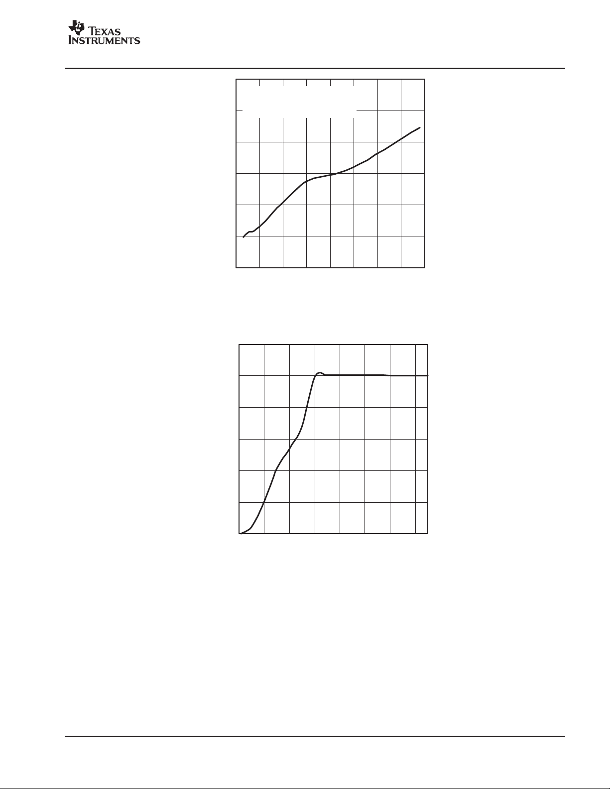
ac-coupling capacitors. For example, by using 50-µF capacitors and setting the AIC28 programmable filter
coefficients as shown below, the frequency response can be improved as shown in Figure 21.
Filter coefficients (use the same for both channels):
N0 = 32767, N1 = −32346, N2 = 31925, N3 = 32767, N4 = 0, N5 = 0
D0 = 32738, D1 = −32708, D4 = 0, D5 =0
27

SLAS418A − FEBRUARY 2004 − REVISED SEPTEMBER 2004
0
−2
−4
−6
−8
−10
Gain − dB
−12
−14
−16
−18
−20
0 200 400 600 800 1000
Figure 20. Uncompensated Response For 16-Ω Load and 50-F Decoupling Capacitor
0
−2
www.ti.com
f − Frequency − Hz
−4
−6
−8
−10
Gain − dB
−12
−14
−16
−18
−20
0
200 400 600 800 1000
f − Frequency − Hz
Figure 21. Frequency Response For 16-Ω Load and 50-F Decoupling Capacitor After Gain
Compensation Using Above Set of Coefficients For Audio Effects Filter
Using the capless output configuration eliminates the need for these capacitors and removes the accompanying
high-pass filter entirely. However, this configuration does have one drawback – if the RETURN terminal of the
headphone jack (which is wired to the AIC28 VGND pin) is ever connected to a ground that is shorted to the
AIC28 ground pin, then the VGND amplifier enters short-circuit protection, and the audio output does not
function properly.
The AIC28 incorporates a programmable short-circuit detection/protection function. In case of short circuit, all
analog outputs are disabled and a read only bit D1 of control register 1DH/page 2 is set. In such cases, there
are two ways to return to normal operation:
− Hardware or software reset
− Power down all the output drivers, which can be achieved by setting bits D12, D1 1, D 8, D7, and D6 of control
register 05H/page 2 and then wait for driver power down status flags (bits D15−D10 of control register
25H/page 2) to become 1. The wait time is typically less than 50 ms after which, output drivers can be
programmed as desired.
28

www.ti.com
SLAS418A − FEBRUARY 2004 − REVISED SEPTEMBER 2004
For the cap interface, this feature can be disabled by setting bit D0 of control register 20H/page 2. In the case
of the cap-less interface, VGND short circuit protection must also be disabled, which can be achieved by setting
bit D4 of control register 21H/page 2.
The AIC28 implements a pop reduction scheme to reduce audible artifacts during powerup and powerdown of
headphone drivers. The scheme can be controlled by programming bits D5 and D4 of control register 25H/page
2. By default, the driver pop reduction scheme is enabled and can be disabled by programming bit D5 of control
register 25H/page 2 to 1. When this scheme is enabled and the virtual ground connection is not used (VGND
amplifier is powered down), the audio output driver slowly charges up any external ac-coupling capacitors to
reduce audible artifacts. Bit D4 of control register 25H/page 2 provides control of the charging time for the
ac-coupling capacitor as either 0.8 sec or 4 sec. When the virtual ground amplifier is powered up and used, the
external ac-coupling capacitor is eliminated, and the powerup time becomes 1 ms. This scheme takes effect
whenever any of the headphone drivers are powered up.
D Speaker Driver
The AIC28 has an integrated speaker driver (OUT8P−OUT8N) capable of driving an 8 Ω differential load. The
speaker driver, powered directly from the battery supply (3.5 V to 4.2 V) on the BVDD pin can deliver 400 mW
at 3.9 V supply. It allows connecting one or both DAC channel to speaker driver. The AIC28 also has a short
circuit protection feature for the speaker driver which can be enabled by setting bit D5 of control register
21H/page 2.
D Receiver Driver
The AIC28 includes a receiver driver (SPK1−OUT32N), which can drive a 32 Ω differential load. It is capable
of delivering 82 mW into a 32 Ω load. The AIC28 does not allow both the receiver driver and headphone
drivers to be turned on at the same time. Also, when the receiver driver is being used, the headphone driver
load must be disconnected.
Headset Interface
The AIC28 supports all standard headset interfaces. It is capable of interfacing with 3-wire stereo headset,
3-wire cellular headset and 4-wire stereo-cellular headsets. It supports both capacitor-coupled (cap) and
capacitor-less (capless) interface for headset through software programming.
D Capless Interface
Figure 22 shows the connection diagram to the AIC28 for capless interface. VGND acts as a ground of
headset jack. Voltage at VGND is 1.5 V and MICBIAS_HED voltage is programmed to 3.3 V. With this, the
voltage across microphone is configured to be 1.8 V. In order to minimize the effect of routing resistance on
VGND inside the device and on the printed circuit board (PCB), SPKFC should be shorted to VGND at the
jack. This reduces crosstalk from speaker to microphone because of common ground as VGND.
29

SLAS418A − FEBRUARY 2004 − REVISED SEPTEMBER 2004
www.ti.com
MICBIAS_HND
2.5
MICIN_HND
Cellular
Stereo +
Cellular
gm
m = mic
s = stere
g = ground/midbias
D Cap Interface
LOUDSPEAKER
MIC_DETECT_IN
sgStereo
s
s
sgms
RECEIVER
OUT8N
MICBIAS_HED
MICIN_HED
OUT32N
SPKFC
Figure 22. Connection Diagram for Capless Interface
OUT8P
SPK1
SPK2
VGND
−1
3.3V
To Detection block
−1
To Detection
block
1.5 V
Figure 23 shows connection diagram to device for cap interface.
30

www.ti.com
SLAS418A − FEBRUARY 2004 − REVISED SEPTEMBER 2004
MICBIAS_HND
2.5V
MICIN_HND
Cellular
Stereo +
Cellular
gm
m = mic
s = stere
g = ground/midbias
D Auto Detection
LOUDSPEAKER
MIC_DETECT_IN
sgStereo
s
s
RECEIVER
sgm s
OUT8P
OUT8N
MICBIAS_HED
MICIN_HED
OUT32N
SPK1
SPK2
SPKFC
VGND
−1
2.5V
To Detection block
−1
To Detection
block
1.5 V
Figure 23. Connection Diagram for Cap Interface
The AIC28 has built in monitors to automatically detect the insertion and removal of headsets. The detection
scheme can differentiate between stereo, cellular and stereo-cellular headsets. Upon detection of headset
insertion or removal, the AIC28 updates read-only bit D12 of control register 22H/Page 2. The AIC28 can be
programmed to send an active high interrupt for insertion and removal of headsets to the host-processor over
GPIO1 using bit D3 of control register 22H/Page 2 and GPIO2 using bit D4 of control register 22H/Page 2. The
headset detection feature can be enabled by setting bit D15 of control register 22H/Page 2. When headset
detection is enabled and headset is not detected, SPK1, VGND and MICBIAS_HED are turned off irrespective
of control register settings. The AIC28 also has the capability to detect button press on the headset microphone.
It consumes less than 50 µA while waiting for button press with everything else powered down. Upon button
press, the AIC28 updates read-only bit D11 of control register 22H/Page 2. It can also send an active high
interrupt for indicating button press to the processor over GPIO1 using bit D1D0 of control register 22H/Page
2. The AIC28 provides debounce programmability for headset and button detect. Debounce programmability
can be used to reject glitches generated, and hence avoids false detection, while inserting headset or pressing
button.
Figure 24 shows terminal connections and jack configuration required for various headsets. Care should be
taken to avoid any dc path from MIC_DETECT_IN to ground, when a headset is not inserted.
31

SLAS418A − FEBRUARY 2004 − REVISED SEPTEMBER 2004
s
www.ti.com
s
s
g
s
m
Stereo +
Cellular
gms
s
g
m
gmCellular
g
s
s
Figure 24. Connection Diagram for Jacks
D Headset Detection
− Interrupt polarity: Active high.
− Typical interrupt duration: 1.75 ms.
− Debounce programmability on bits D10 and D9 in control register 22H/Page 2:
− 00 => 16 ms duration (with 2 ms clock resolution)
− 01 => 32 ms duration (with 4 ms clock resolution)
− 10 => 64 ms duration (with 8 ms clock resolution)
− 11 => 128 ms duration (with 16 ms clock resolution)
− Headset detect flag is available till headset is connected.
ssgStereo
D Button Detection
− Interrupt polarity: Active high.
− Typical interrupt duration: Button pressed time + clock resolution. Clock resolution depends upon
debounce programmability.
− Typical interrupt delay from button: Debounce duration + 0.5ms
− Debounce programmability:
− 00 => No glitch rejection
− 01 => 8 ms duration (with 1 ms clock resolution)
− 10 => 16 ms duration (with 2 ms clock resolution)
− 11 => 32 ms duration (with 4 ms clock resolution)
− Button detect flag is set when button is pressed. It gets clear when flag read is done after button press
removal.
AUDIO ROUTING
Audio Interface for Smart-Phone Applications
The AIC28 supports audio routing features to combine various analog inputs and route them to analog outputs
or the ADC for smart−phone applications. In smart-phone applications, the AIC28 can be used to interface the
cell-phone module to microphones and speakers. The AIC28 allows the input from the cell-phone module to
be routed to different speakers through a PGA which supports a range of 12 dB to –34.5 dB in steps of 0.5 dB.
The cell-phone input can also be mixed with the microphone input for recording through the ADC. The
microphone or DAC audio can be routed to the cell-phone output. The buzzer input from cell-phone can be
routed to the speakers through a PGA. The buzzer input supports PGA range of 0 dB to –45 dB in steps of 3
dB. The mixing and PGA are under full software control. The mixing feature can be used even when both ADC
and DAC are powered down. Cell-phone PGA, microphone PGA and buzzer PGA includes soft-stepping logic.
Soft-stepping logic works on Fsref if DAC is powered up otherwise; it works on internal oscillator clocks.
32

www.ti.com
SLAS418A − FEBRUARY 2004 − REVISED SEPTEMBER 2004
Analog Mixer
The analog mixer can be used to route the analog input selected for the ADC through an analog volume control
and then mix it with the audio DAC output. The analog mixer feature is available only if the single ended
microphone input or the AUX input is selected as the input to the ADC, not when the ADC input is configured
in fully-differential mode. This feature is available even if the ADC and DAC are powered down. The analog
volume control has a range from +12 dB to –34.5 dB in 0.5 dB steps plus mute and includes soft−stepping logic.
The internal oscillator is used for soft−stepping whenever the ADC and DAC are powered down.
Keyclick
A special circuit has been included for inserting a square−wave signal into the analog output signal path based
on register control. This functionality is intended for generating keyclick sounds for user feedback. Register
04H/Page 2 contains bits that control the amplitude, frequency, and duration of the square−wave signal. The
frequency of the signal can be varied from 62.5 Hz to 8 kHz and its duration can be programmed from 2 periods
to 32 periods. Whenever this register is written, the square wave is generated and coupled into the audio output.
The keyclick enable bit D15 of control register 04H/Page 2 is reset after the duration of a keyclick is played out.
This capability is available even when the ADC and DAC are powered down.
OPERATION—AUXILIARY MEASUREMENT
Auxiliary ADC Converter
The auxiliary analog inputs (battery voltage monitor, chip temperature, and auxiliary inputs) are provided via
a multiplexer to the successive approximation register (SAR) analog-to-digital (A/D) converter. The ADC
architecture is based on capacitive redistribution architecture, which inherently includes a sample/hold function.
The ADC is controlled by an ADC control register. Several modes of operation are possible, depending upon
the bits set in the control register. Channel selection, scan operation, averaging, resolution, and conversion rate
may all be programmed through this register. These modes are outlined in the sections below for each type of
analog input. The results of conversions made are stored in the appropriate result register.
Data Format
The AIC28 output data is in unsigned Binary format and can be read from registers over the SPI interface.
Reference
The AIC28 has an internal voltage reference that can be set to 1.25 V or 2.5 V, through the reference control
register.
The internal reference voltage should only be used in the single-ended mode for battery monitoring,
temperature measurement, and for utilizing the auxiliary inputs.
An external reference can also be applied to the VREF pin, and the internal reference can be turned off.
Variable Resolution
The AIC28 provides three different resolutions for the ADC: 8, 10 or 12 bits. Performing the conversions at lower
resolution reduce the amount of time it takes for the ADC to complete its conversion process, which lowers
power consumption.
Conversion Clock and Conversion Time
The AIC28 contains an internal 8 MHz clock, which is used to drive the state machines inside the device that
perform the many functions of the part. This clock is divided down to provide a clock to run the ADC. The division
ratio for this clock is set in the ADC control register. The ability to change the conversion clock rate allows the
user to choose the optimal value for resolution, speed, and power. If the 8 MHz clock is used directly, the ADC
is limited to 8-bit resolution; using higher resolutions at this speed does not result in accurate conversions. Using
a 4 MHz conversion clock is suitable for 10-bit resolution; 12-bit resolution requires that the conversion clock
run at 1 or 2 MHz.
Regardless of the conversion clock speed, the internal clock runs nominally at 8 MHz. The conversion time of
the AIC28 is dependent upon several functions. While the conversion clock speed plays an important role in
the time it takes for a conversion to complete, a certain number of internal clock cycles are needed for proper
33

SLAS418A − FEBRUARY 2004 − REVISED SEPTEMBER 2004
sampling of the signal. Moreover, additional times, such as the panel voltage stabilization time, can add
significantly to the time it takes to perform a conversion. Conversion time can vary depending upon the mode
in which the AIC28 is used. Throughout this data sheet, internal and conversion clock cycles are used to
describe the times that many functions take to execute. Considering the total system design, these times must
be taken into account by the user.
When both the audio ADC and DAC are powered down, the auxiliary ADC uses an internal oscillator for
conversions. However, to save power whenever audio ADC or DAC are powered up, the internal oscillator is
powered down and MCLK and BCLK are used to clock the auxiliary ADC.
The AIC28 uses the programmed value of bit D13 in control register 06H/page 2 and the PLL programmability
to derive a clock from MCLK. The various combinations are listed in Table 3.
Table 3. Conversion Clock Frequency
D13=0 (in control register 06H/page 2) D13=1 (in control register 06H/page 2)
www.ti.com
PLL enabled
PLL disabled
MCLK
P
MCLK
Q
×
×
K
160
×
10
13
13
××
P
MCLK
Q
×
×
KMCLK
192
×
12
17
17
××
Temperature Measurement
In some applications, such as battery charging, a measurement of ambient temperature is required. The
temperature measurement technique used in the AIC28 relies on the characteristics of a semiconductor
junction operating at a fixed current level. The forward diode voltage (VBE) has a well-defined characteristic
versus temperature. The ambient temperature can be predicted in applications by knowing the 25°C value of
the VBE voltage and then monitoring the variation of that voltage as the temperature changes.
The AIC28 offers two modes of temperature measurement. The first mode requires a single reading to predict
the ambient temperature. A diode, as shown in Figure 25, is used during this measurement cycle. This voltage
is typically 600 mV at +25°C with a 20-µA current through it. The absolute value of this diode voltage can vary
a few millivolts. The temperature coefficient of this voltage is typically 2 mV/°C. During the final test of the end
product, the diode voltage at a known room temperature should be stored in nonvolatile memory. Further
calibration can be done to calculate the precise temperature coefficient of the particular. This method has a
temperature resolution of approximately 0.3°C/LSB and accuracy of approximately ±2°C with two-temperature
calibration. Figure 26 and Figure 27 shows typical plots with single and two-temperature calibration
respectively.
34
X+
MUX
Temperature Select
TEMP0 TEMP1
A/D
Converter
Figure 25. Functional Block Diagram of Temperature Measurement Mode

www.ti.com
SLAS418A − FEBRUARY 2004 − REVISED SEPTEMBER 2004
10
8
6
C
°
4
2
0
−2
−4
Error in Measurement −
−6
−8
−10
−40 −20 0 20 40 60 80 100
TA − Free-Air Temperature − C
Figure 26. Typical Plot of Single Measurement Method After Calibrating for Offset at Room Temperature
0.20
0
C
°
−0.20
−0.40
−0.60
−0.80
Error in Measurement −
−1
−1.20
−40 −20 0 20 40 60 80 100
TA − Free-Air Temperature − C
Figure 27. Typical Plot of Single Measurement Method After Calibrating for Offset and Gain At Two
Temperatures
The second mode uses a two-measurement (differential) method. This mode requires a second conversion with
a current 82 times larger. The voltage difference between the first (TEMP1) and second (TEMP2) conversion,
using 82 times the bias current, is represented by:
kT
ln(N)
q
where:
N is the current ratio = 82
k = Boltzmann’s constant (1.38054 • 10
q = the electron charge (1.602189 • 10
−23
electrons volts/degrees Kelvin)
−19
°C)
T = the temperature in degrees Kelvin
The equation for the relation between differential code and temperature may vary slightly from device to device
and can be calibrated at final system test by the user. This method provides resolution of approximately
1.5°C/LSB and accuracy of approximately ±4°C after calibrating at room temperature.
35

SLAS418A − FEBRUARY 2004 − REVISED SEPTEMBER 2004
4
3
C
°
2
1
0
−1
Error in Measurement −
−2
−3
−4
−40 −20 0 20 40 60 80 100
www.ti.com
TA − Free-Air Temperature − C
Figure 28. Typical Plot of Differential Measurement Method After Calibrating for Offset at Room
Temperature
The AIC28 supports programmable auto-temperature measurement mode, which can be enabled using control
register 0CH/page 1. In this mode, the AIC28 can auto-start the temperature measurement after a
programmable interval. The user can program minimum and maximum threshold values through a register. If
the measurement goes outside the threshold range, the AIC28 sets a flag in the read only control register
0CH/page 1, which gets cleared after the flag is read. The AIC28 can also be configured to send and active
high interrupt over GPIO1 by setting D9 in control register 0CH/page 1. The duration of the interrupt is
approximately 2 ms.
Battery Measurement
An added feature of the AIC28 is the ability to monitor the battery voltage on the other side of a voltage regulator
(dc/dc converter), as shown in Figure 29. The battery voltage can vary from 0.5 V to 6 V while maintaining the
analog supply voltage to the AIC28 at 3.0 V to 3.6 V. The input voltage (VBAT) is divided down by a factor of
5 so that a 6.0 V battery voltage is represented as 1.2 V to the ADC. In order to minimize the power consumption,
the divider is only on during the sampling of the battery input.
If the battery conversion results in A/D output code of B, the voltage at the battery pin can be calculated as:
V
BAT
B
+
5 VREF
N
2
Where:
N is the programmed resolution of A/D
VREF is the programmed value of internal reference or the applied external reference.
36

www.ti.com
SLAS418A − FEBRUARY 2004 − REVISED SEPTEMBER 2004
3.0 V to 3.6 V
V
2 kΩ
DD
ADC
Battery
0.5 to 6 V
LDO or DC-DC
Converter
+
−
R
VBAT
8 kΩ
Figure 29. Battery Measurement Functional Block Diagram
See the section Conversion Time Calculation for the AIC28 in this data sheet for timing diagrams and
conversion time calculations.
For increased protection and robustness, TI recommends a minimum 100−Ω resistor be added in series
between the system battery and the VBAT pin. The 100-Ω resistor will cause an approximately 1% gain change
in the battery voltage measurement, which can easily be corrected in software when the battery conversion data
is read by the operating system.
Auxiliary Measurement
The auxiliary voltage inputs (AUX1 and AUX2) can be measured in much the same way as the battery inputs
except the d i fference that input voltage is not divided. Applications might include external temperature sensing,
ambient light monitoring for controlling the backlight, or sensing the current drawn from the battery. The auxiliary
input can also be monitored continuously in scan mode.
The AIC28 provides feature to measure resistance using auxiliary inputs. It has two modes of operation: (1)
External bias resistance measurement (2) Internal bias resistance measurement. Internal bias resistance
measurement mode does not need an external bias resistance of 50 kΩ, but provides less accuracy because
of on chip resistance variation, which is typically ±20%. Figure 30 shows connection diagram for resistance
measurement mode on AUX1.
VREF
50 kΩ
AUX1
R
a. Internal bias, Resistance Measurement
Vsar
SAR
50 kΩ
AUX1
R
b. External bias, Resistance Measurement
VREF
50 kΩ
Vsar
SAR
Figure 30. Connection DIagram for Resistance Measurement
Resistance can be calculated using following formula:
R + 50 KW
Vsar
VREF* Vsar
Where:
37

SLAS418A − FEBRUARY 2004 − REVISED SEPTEMBER 2004
VREF is the SAR ADC reference
Vsar is input to the SAR ADC
The AIC28 supports programmable auto−auxiliary measurement mode, which can be enabled using control
register 0CH/page 1. In this mode, the AIC28 can auto start the auxiliary measurement after a programmable
interval. The user can program minimum and maximum threshold values through a register . If the measurement
goes outside the threshold range, the AIC28 sets a flag in the read only control register 0CH/page 1, which gets
cleared after the flag is read. The AIC28 can also be configured to send an active high interrupt over GPIO1
by setting D9 of control register 0CH/page 1. The duration of the interrupt is approximately 2 ms.
See the section Conversion Time Calculation for the AIC28 in this data sheet for timing diagram and conversion
time calculation
Port Scan
If making measurements of VBAT, AUX1, and AUX2 is desired on a periodic basis, the Port Scan mode can
be used. This mode causes the AIC28 to sample and convert battery input and both auxiliary inputs. At the end
of this cycle, the battery and auxiliary result registers contain the updated values. Thus, with one write to the
AIC28, the host can cause three different measurements to be made.
See the section Issues at the end of this data sheet for details of a known issue with this mode.
See the section Conversion Time Calculation for the AIC28 and subsection Port Scan Operation in this data
sheet for timing diagrams and conversion time calculations.
Buffer Mode
The AIC28 supports a programmable buffer mode, which is applicable auxiliary (BAT, AUX1, AUX2, TEMP1,
TEMP2). Buffer mode is implemented using a circular FIFO with a depth of 64. The number of interrupts
required to be serviced by a host processor can be reduced significantly buffer mode. Buffer mode can be
enabled using control register 02H/page1.
www.ti.com
Figure 31. Circular Buffer
Converted data is automatically written into the FIFO. To control the writing, reading and interrupt process, a
write pointer (WRPTR), a read pointer (RDPTR) and a trigger pointer (TGPTR) are used. The read pointer
always shows the location, which will be read next. The write pointer indicates the location, in which the next
converted data is going to be written. The trigger pointer indicates the location at which an interrupt will be
generated if the write pointer reaches that location. Trigger level is the number of the data points needed to be
present in the FIFO before generating an interrupt. Figure 31 shows the case when trigger level is programmed
as 32. On resetting buffer mode, RDPTR moves to location 1, WRPTR moves to location 1, and TGPTR moves
to location equal to programmed trigger level.
38

www.ti.com
SLAS418A − FEBRUARY 2004 − REVISED SEPTEMBER 2004
The user can select the input or input sequence, which needs to be converted, from the ADCSM bits of control
register 00H/page 1. The converted values are written in a predefined sequence to the circular buffer. The user
has flexibility to program a specific trigger level in order to choose the configuration which best fits the
application. When the number of converted data, written in FIFO, becomes equal to the programmed trigger
level then the device generates an interrupt signal on DAV
Buffer mode can be used in single-shot conversion or continuous conversion mode.
In single shot conversion mode, once the number of data written reaches programmed trigger level, the AIC28
generates an interrupt and waits for the user to start reading. As soon as the user starts reading the first data
from the last converted set, the AIC28 clears the interrupt and starts a new set of conversions and the trigger
pointer is incremented by the programmed trigger level. An interrupt is generated again when the trigger
condition is satisfied.
In continuous conversion mode, once number of data written reaches the programmed trigger level, the AIC28
generates an interrupt. It immediately starts a new set of conversions and the trigger pointer is incremented
by the programmed trigger level. An interrupt gets cleared either by writing the next converted data into the FIFO
or by starting to read from the FIFO.
See the section Conversion Time Calculation for the AIC28 and subsection Buffer Mode Operation in this data
sheet for timing diagrams and conversion time calculations.
Depending upon how the user is reading data, the FIFO can become empty or full. If the user is trying to read
data even if the FIFO is empty, then RDPTR keeps pointing to same location. If the FIFO gets full then the next
location is overwritten with newly converted data and the read pointer is incremented by one.
While reading the FIFO, the AIC28 provides FIFO empty and full status flags along with the data. The user can
also read a status flag from control register 02H/page 1.
pin.
DIGITAL INTERFACE
RESET
The device requires reset after power up. This requires a low-to-high transition on the RESET pin after power
up for correct operation. Reset initializes all the internal registers, counters and logic.
Hardware Power-Down
Hardware power-down powers down all the internal circuitry to save power. All the register contents are
maintained.
General Purpose I/O
The AIC28 has two general purpose I/O (GPIO1 and GPIO2), which can be programmed either as inputs or
outputs. As outputs they can be programmed to control external logic through the AIC28 registers or send
interrupts to the host processor on events like button detect, headset insertion, headset removal,
Auxiliary/temperature outside threshold range etc. As inputs they can be used by the host-processor to monitor
logic states of signals on the system through the AIC28 registers.
SPI Digital Interface
All AIC28 control registers are programmed through a standard SPI bus. The SPI allows full-duplex,
synchronous, serial communication between a host processor (the master) and peripheral devices (slaves).
The SPI master generates the synchronizing clock and initiates transmissions. The SPI slave devices depend
on a master to start and synchronize transmissions.
A transmission begins when initiated by a master SPI. The byte from the master SPI begins shifting in on the
slave MOSI pin under the control of the master serial clock. As the byte shifts in on the MOSI pin, a byte shifts
out on the MISO pin to the master shift register.
The idle state of the serial clock for the AIC28 is low, which corresponds to a clock polarity setting of 0 (typical
microprocessor SPI control bit CPOL = 0). The AIC28 interface is designed so that with a clock phase bit setting
of 1 (typical microprocessor SPI control bit CPHA = 1), the master begins driving its MOSI pin and the slave
begins driving its MISO pin on the first serial clock edge. The SS pin can remain low between transmissions;
however, the AIC28 only interprets command words which are transmitted after the falling edge of SS.
39

SLAS418A − FEBRUARY 2004 − REVISED SEPTEMBER 2004
AIC28 COMMUNICATION PROTOCOL
Register Programming
The AIC28 is entirely controlled by registers. Reading and writing these registers is controlled by an SPI master
and accomplished by the use of a 16-bit command, which is sent prior to the data for that register. The command
is constructed as shown in Figure 32.
The command word begins with an R/W bit, which specifies the direction of data flow on the SPI serial bus. The
following 4 bits specify the page of memory this command is directed to, as shown in Table 4. The next six bits
specify the register address on that page of memory to which the data is directed. The last five bits are reserved
for future use and should be written only with zeros.
Table 4. Page Addressing
PG3 PG2 PG1 PG0 PAGE ADDRESSED
0 0 0 0 0
0 0 0 1 1
0 0 1 0 2
0 0 1 1 3
0 1 0 0 Reserved
0 1 0 1 Reserved
0 1 1 0 Reserved
0 1 1 1 Reserved
1 0 0 0 Reserved
1 0 0 1 Reserved
1 0 1 0 Reserved
1 0 1 1 Reserved
1 1 0 0 Reserved
1 1 0 1 Reserved
1 1 1 0 Reserved
1 1 1 1 Reserved
www.ti.com
T o read all the first page of memory, for example, the host processor must send the AIC28 the command 0x8000
– this specifies a read operation beginning at page 0, address 0. The processor can then start clocking data
out of the AIC28. The AIC28 automatically increments its address pointer to the end of the page; if the host
processor continues clocking data out past the end of a page, the AIC28 sends back the value 0xFFFF.
Likewise, writing to page 1 of memory would consist of the processor writing the command 0x0800, which
specifies a write operation, with PG0 set to 1, and all the ADDR bits set to 0. This results in the address pointer
pointing at the first location in memory on page 1. See the section on the AIC28 memory map for details of
register locations.
BIT 15
BIT 14 BIT 13 BIT 12 BIT 11 BIT 10 BIT 9 BIT 8 BIT 7 BIT 6 BIT 5 BIT 4 BIT 3 BIT 2 BIT 1 BIT 0
MSB
R/W* PG3 PG2 PG1 PG0 ADDR5 ADDR4 ADDR3 ADDR2 ADDR1 ADDR0 0 0 0 0 0
Figure 32. AIC28 Command Word
SS
SCLK
MOSI
COMMAND WORD
DATA
DATA
Figure 33. Register Write Opration
40
LSB

www.ti.com
SCLK
SLAS418A − FEBRUARY 2004 − REVISED SEPTEMBER 2004
SS
MOSI
MOSO
COMMAND WORD
DATA
DATA
Figure 34. Register Read Operation
AIC28 Memory Map
The AIC28 has several 16-bit registers which allow control of the device as well as providing a location for results
from the AIC28 to be stored until read by the host microprocessor. These registers are separated into four pages
of memory in the AIC28: a data page (page 0), control pages (page 1 and page 2) and a buffer data page (page
3). The memory map is shown in Table 5.
Table 5. Memory Map
PAGE 0: AUXILIARY
DATA REGISTER
ADDR REGISTER ADDR REGISTER ADDR REGISTER ADDR REGISTER
00 Reserved 00 AUX ADC 00 Audio Control 1 00 Buffer Location
01 Reserved 01 Status 01 Headset PGA Control 01 Buffer Location
02 Reserved 02 Buffer Mode 02 DAC PGA Control 02 Buffer Location
03 Reserved 03 Reference 03 Mixer PGA Control 03 Buffer Location
04 Reserved 04 Reset Control Register 04 Audio Control 2 04 Buffer Location
05 BAT 05 Configuration 05 Power Down Control 05 Buffer Location
06 Reserved 06 Temperature Max 06 Audio Control 3 06 Buffer Location
07 AUX1 07 T emperature Min 07 Digital Audio Effects Filter Coefficients 07 Buffer Location
08 AUX2 08 AUX1 Max 08 Digital Audio Effects Filter Coefficients 08 Buffer Location
09 TEMP1 09 AUX1 Min 09 Digital Audio Effects Filter Coefficients 09 Buffer Location
0A TEMP2 0A AUX2 Max 0A Digital Audio Effects Filter Coefficients 0A Buffer Location
0B Reserved 0B AUX2 Min 0B Digital Audio Effects Filter Coefficients 0B Buffer Location
0C Reserved 0C Measurement Configuration 0C Digital Audio Effects Filter Coefficients 0C Buffer Location
0D Reserved 0D Programmable Delay 0D Digital Audio Effects Filter Coefficients 0D Buffer Location
0E Reserved 0E Reserved 0E Digital Audio Effects Filter Coef ficients 0E Buffer Location
0F Reserved 0F Reserved 0F Digital Audio Effects Filter Coefficients 0F Buffer Location
10 Reserved 10 Reserved 10 Digital Audio Effects Filter Coefficients 10 Buffer Location
11 Reserved 11 Reserved 11 Digital Audio Effects Filter Coefficients 11 Buffer Location
12 Reserved 12 Reserved 12 Digital Audio Effects Filter Coefficients 12 Buffer Location
13 Reserved 13 Reserved 13 Digital Audio Effects Filter Coefficients 13 Buffer Location
14 Reserved 14 Reserved 14 Digital Audio Effects Filter Coefficients 14 Buffer Location
15 Reserved 15 Reserved 15 Digital Audio Effects Filter Coefficients 15 Buffer Location
16 Reserved 16 Reserved 16 Digital Audio Effects Filter Coefficients 16 Buffer Location
17 Reserved 17 Reserved 17 Digital Audio Effects Filter Coefficients 17 Buffer Location
18 Reserved 18 Reserved 18 Digital Audio Effects Filter Coefficients 18 Buffer Location
19 Reserved 19 Reserved 19 Digital Audio Effects Filter Coefficients 19 Buffer Location
1A Reserved 1A Reserved 1A Digital Audio Effects Filter Coef ficients 1A Buffer Location
PAGE 1: AUXILIARY CONTROL
REGISTERS
PAGE 2: AUDIO CONTROL REGISTERS
PAGE 3: BUFFER
DATA REGISTERS
41

SLAS418A − FEBRUARY 2004 − REVISED SEPTEMBER 2004
www.ti.com
PAGE 0: AUXILIARY
DATA REGISTER
1B Reserved 1B Reserved 1B PLL Programmability 1B Buffer Location
1C Reserved 1C Reserved 1C PLL Programmability 1C Buffer Location
1D Reserved 1D Reserved 1D Audio Control 4 1D Buffer Location
1E Reserved 1E Reserved 1E Handset PGA Control 1E Buffer Location
1F Reserved 1F Reserved 1F Cell & Buzzer PGA Control 1F Buffer Location
20 Reserved 20 Reserved 20 Audio Control 5 20 Buffer Location
21 Reserved 21 Reserved 21 Audio Control 6 21 Buffer Location
22 Reserved 22 Reserved 22 Audio Control 7 22 Buffer Location
23 Reserved 23 Reserved 23 GPIO Control 23 Buffer Location
24 Reserved 24 Reserved 24 AGC−CP_IN Control 24 Buffer Location
25 Reserved 25 Reserved 25 Driver Powerdown Status 25 Buffer Location
26 Reserved 26 Reserved 26 Mic AGC control 26 Buffer Location
27 Reserved 27 Reserved 27 Cell-phone AGC Control 27 Buffer Location
28 Reserved 28 Reserved 28 Reserved 28 Buffer Location
29 Reserved 29 Reserved 29 Reserved 29 Buffer Location
2A Reserved 2A Reserved 2A Reserved 2A Buffer Location
2B Reserved 2B Reserved 2B Reserved 2B Buffer Location
2C Reserved 2C Reserved 2C Reserved 2C Buffer Location
2D Reserved 2D Reserved 2D Reserved 2D Buffer Location
2E Reserved 2E Reserved 2E Reserved 2E Buffer Location
2F−3F Reserved 2F−3F Reserved 2F−3F Reserved 2F−3F Buffer
PAGE 1: AUXILIARY CONTROL
REGISTERS
PAGE 2: AUDIO CONTROL REGISTERS
PAGE 3: BUFFER
DATA REGISTERS
REGISTERADDRREGISTERADDRREGISTERADDRREGISTERADDR
Locations
AIC28 Control Registers
This section describes each of the registers shown in the memory map of Table 5. The registers are grouped
according to the function they control. Note that in the AIC28, bits in control registers may refer to slightly
different functions depending upon if you are reading the register or writing to it.
AIC28 Data Registers (Page 0)
The data registers of the AIC28 hold data results from conversion of auxiliary ADC. All of these registers default
to 0000H upon reset. These registers are read only.
BAT, AUX1, AUX2, TEMP1 and TEMP2 Registers
The results of all ADC conversions are placed in the appropriate data register. The data format of the result
word, R, of these registers is right-justified, as follows:
Bit 15
MSB
Bit 14 Bit 13 Bit 12 Bit 11 Bit 10 Bit 9 Bit 8 Bit 7 Bit 6 Bit 5 Bit 4 Bit 3 Bit 2 Bit 1 Bit 0
0 0 0 0 R11
MSB
R10 R9 R8 R7 R6 R5 R4 R3 R2 R1 R0
LSB
LSB
42

www.ti.com
SLAS418A − FEBRUARY 2004 − REVISED SEPTEMBER 2004
PAGE 1 CONTROL REGISTER MAP
REGISTER 00H: Auxiliary ADC Control
BIT NAME
D15 0 R Reserved. The value of this bit should always be set to zero.
D14 ADST 1(for read)
D13−D10 ADCSM 0000 R/W ADC Scan Mode.
D9−D8 RESOL 00 R/W Resolution Control. The ADC resolution is specified with these bits.
D7−D6 ADAVG 00 R/W Converter Averaging Control. These two bits allow user to specify the number of averages the
RESET
VALUE
0 (for write)
READ/
WRITE
R/W ADC STATUS.
READ
0 =>ADC is busy
1 => ADC is not busy (default).
WRITE
0 => Normal mode (default).
1 => Stop conversion and power down.
0000 => No scan
0001 => Reserved
0010 => Reserved
0011 => Reserved
0100 => Reserved
0101 => Reserved
0110 => BAT input is converted and the results returned to the BAT data register.
0111 => AUX2 input is converted and the results returned to the AUX2 data register
1000 => AUX1 input is converted and the results returned to the AUX1 data register.
1001 => Auto Scan function: For AUX1, AUX2, TEMP1 or TEMP2 as chosen using control
1010 => TEMP1 input is converted and the results returned to the TEMP1 data register.
1011 => Port scan function: BAT , AUX1, AUX2 inputs are measured and the results returned to
1100 => TEMP2 input is converted and the results returned to the TEMP2 data register.
1101 => Reserved
1110 => Reserved
1111 => Reserved
00 => 12-bit resolution
01 => 8-bit resolution
10 => 10-bit resolution
11 => 12-bit resolution
converter will perform selected by bit D0, which selects either Mean Filter or Median Filter.
FUNCTION
register 0CH/page 1. Scan continues until stop bit is sent or D13−D10 are changed.
the appropriate data registers.
Mean Filter Median Filter
00 => No average No average
01 => 4-data average 5-data average
10 => 8-data average 9-data average
11 => 16-data average 15-data average
D5−D4 ADCR 00 R/W Conversion Rate Control. These two bits specify the internal clock rate, which the ADC uses to
control performing a single conversion. These bits are the same whether reading or writing.
t
conv
Where f
INTCLK
internal clock frequency, the conversion time is 8 µs. This yields an effective throughput rate of
125 kHz.
00 => 8 MHz internal clock rate (use for 8-bit resolution only)
01 =>4 MHz internal clock rate (use for 8-bit/10-bit resolution only)
10 =>2 MHz internal clock rate
11 =>1 MHz internal clock rate
D3−D1 0’s R Reserved
D0 AVGFS 0 R/W Average Filter Select
0 => Mean Filter
1 => Median Filter
N ) 4
+
ƒ
INTCLK
is the internal clock frequency. For example, with 12-bit resolution and a 2 MHz
43

SLAS418A − FEBRUARY 2004 − REVISED SEPTEMBER 2004
REGISTER 01H: Status Register
BIT NAME
D15−D14 DAV 10 R/W Data Available. These two bits program the function of the DAV pin.
D13 PWRDN 0 R ADC Power down status
D12 0 R Reserved
D11 DAVAIL 0 R Data Available Status
D10−D7 0 R Reserved
D6 BSTAT 0 R BAT Data Register Status
D5 0 R Reserved
D4 AX1STAT 0 R AUX1 Data Register Status
D3 AX2STAT 0 R AUX2 Data Register Status
D2 T1STAT 0 R TEMP1 Data Register Status
D1 T2STAT 0 R TEMP2 Data Register Status
D0 0 R Reserved
RESET
VALUE
READ/
WRITE
FUNCTION
00 => Reserved
01 => Acts as data available (active low) only. The DAV goes low as soon as one set of ADC
conversion(s) is completed. For scan mode, DAV remains low as long as all the
appropriate registers have not been read out.
10 => Reserved
11 => Reserved
Note:− D15−D14 should be rpogrammed to 01 for the AIC28 to operate properly.
0 => ADC is active
1 => ADC stops conversion and powers down
0 => No data available.
1 => Data is available(i.e one set of conversion is done)
Note:− This bit gets cleared only after all the converted data have been completely read out. This bit
is not valid in case of buffer mode.
0 => No new data is available in BAT data register
1 => New data is available in BAT data register
Note: This bit gets cleared only after the converted data of BAT has been completely read out of the
register. This bit is not valid in case of buffer mode.
0 => No new data is available in AUX1−data register
1 => New data is available in AUX1−data register
Note: This bit gets cleared only after the converted data of AUX1 has been completely read out of
the register. This bit is not valid in case of buf fer mode.
0 => No new data is available in AUX2−data register
1 => New data is available in AUX2−data register
Note: This bit gets cleared only after the converted data of AUX2 has been completely read out of
the register. This bit is not valid in case of buf fer mode.
0 => No new data is available in TEMP1−data register
1 => New data is available in TEMP1−data register
Note: This bit gets cleared only after the converted data of TEMP1 has been completely read out of
the register. This bit is not valid in case of buffer mode.
0 => No new data is available in TEMP2−data register
1 => New data is available in TEMP2−data register
Note: This bit gets cleared only after the converted data of TEMP2 has been completely read out of
the register. This bit is not valid in case of buffer mode.
www.ti.com
44

www.ti.com
SLAS418A − FEBRUARY 2004 − REVISED SEPTEMBER 2004
REGISTER 02H: Buffer Control
BIT NAME
D15 BUFRES 0 R/W Buffer Reset.
D14 BUFCONT 0 R/W Buffer Mode Selection
D13−D11 BUFTL 000 R/W Trigger Level TL selection of Buffer used for SAR ADC
D10 BUFOVF 0 R Buffer Full Flag
D9 BUFEMF 1 R Buffer Empty Flag
D8−D0 0’s R Reserved
RESET
VALUE
READ/
WRITE
FUNCTION
0 => Buffer mode is disabled and RDPTR, WRPTR & TGPTR set to their reset value.
1 => Buffer mode is enabled.
0 => Continuous conversion mode.
1 => Single shot mode.
000 => 8
001 => 16
010 => 24
011 => 32
100 => 40
101 => 48
110 => 56
111 => 64
0 => Buffer is not full.
1 => Buffer is full. This means buffer contains 64 unread converted data.
0 => Buffer is not empty .
1 => Buffer is empty . This means there is no unread converted data in the buffer.
REGISTER 03H: Reference Control
BIT NAME
D15−D6 0’s R Reserved
D5 0 R/W Reserved. Always write 0 to this bit.
D4 VREFM 0 R/W Voltage Reference Mode. This bit configures the VREF pin as either external reference or internal
D3−D2 RPWUDL 00 R/W Reference Power Up Delay . These bits allow for a delay time for measurements to be made after
D1 RPWDN 1 R/W Reference Power Down. This bit controls the power down of the internal reference voltage.
D0 IREFV 0 R/W Internal Reference Voltage. This bit selects the internal voltage for AUX ADC.
RESET
VALUE
READ/
WRITE
FUNCTION
reference.
0 => External reference
1 => Internal reference
the reference powers up, thereby assuring that the reference has settled
00 => 0 µs
01 => 100 µs
10 => 500 µs
11 => 1000 µs
Note: This will be valid only when device is programmed for internal reference and Bit D1 = 1, i.e.,
reference is powered down between the conversions if not required.
0 => Powered up at all times.
1 => Powered Down between conversions.
Note: When D4 = 0 i.e. device is in external reference mode then the internal reference is powered
down always.
0 => VREF = 1.25 V
1 => VREF = 2.50 V
45

www.ti.com
SLAS418A − FEBRUARY 2004 − REVISED SEPTEMBER 2004
REGISTER 04H: Reset Control
BIT NAME
D15−D0 RSALL R/W FFFFH Reset All. Writing the code 0xBB00, as shown below, to this register causes the AIC28 to reset all
RESET
VALUE
REGISTER 05H: Reserved
BIT NAME
D15−D0 0’s R Reserved
RESET
VALUE
REGISTER 06H: Temperature Max Threshold Measurement
BIT NAME
D15−D13 0’s R Reserved
D12 TMXES 0 R/W Max Temperature (TEMP1 or TEMP2) threshold check enable for Auto/Non−Auto−Scan
D11−D0 TTHRESH FFFH R/W Temperature Max Threshold. When code due to temperature measurement goes above or equal
RESET
VALUE
READ/
WRITE
READ/
WRITE
READ/
WRITE
FUNCTION
its control registers to their default, power−up values.
1011101100000000 => Reset all control registers
Others => Do not write other sequences to the register.
FUNCTION
FUNCTION
Measurement.
0 => Max Temperature threshold check is disabled.
1 => Max Temperature threshold check is enabled.
Only valid for TEMP1 or TEMP2. Depends on bit TSCAN of control register 0CH/page 1 in case
of auto−scan measurement and depends on bits ADCSM of control register 00H/page 1 in case
of non−auto−scan measurementa
to programmed threshold value, interrupt is generated.
REGISTER 07H: Temperature Min Threshold Measurement
BIT NAME
D15−D13 0’s R Reserved
D12 TMNES 0 R/W Min Temperature (TEMP1 or TEMP2) threshold check enable for Auto/Non−Auto−Scan
D11−D0 TTHRESL 000H R/W Temperature Min Threshold. When code due to temperature measurement goes below or equal to
RESET
VALUE
READ/
WRITE
FUNCTION
Measurement.
0 => Min Temperature threshold check is disabled.
1 => Min Temperature threshold check is enabled.
Only valid for TEMP1 or TEMP2. Depends on bit TSCAN of control register 0CH/page 1 in case
of auto−scan measurement and depends on bits ADCSM of control register 00H/page 1 in case
of non−auto−scan measurement.
programmed threshold value, interrupt is generated.
REGISTER 08H: AUX1 Max Threshold Measurement
BIT NAME
D15−D13 0’s R Reserved
D12 A1MXES 0 R/W Max AUX1 threshold check enable for Auto/Non−Auto−Scan Measurement.
D11−D0 A1THRESH FFFH R/W AUX1 Threshold. When code due to AUX1 measurement goes above or equal to programmed
RESET
VALUE
READ/
WRITE
FUNCTION
0 => Max AUX1 threshold check is disabled.
1 => Max AUX1 threshold check is enabled.
threshold value, interrupt is generated.
46

www.ti.com
SLAS418A − FEBRUARY 2004 − REVISED SEPTEMBER 2004
REGISTER 09H: AUX1 Min Threshold Measurement
BIT NAME
D15−D13 0’s R Reserved
D12 A1MNES 0 R/W Min AUX1 threshold check enable for Auto/Non−Auto−Scan Measurement.
D11−D0 A1THRESL 000H R/W AUX1 Threshold. When code due to AUX1 measurement goes below or equal to programmed
RESET
VALUE
REGISTER 0AH: AUX2 Max Threshold Measurement
BIT NAME
D15−D13 0’s R Reserved
D12 A2MXES 0 R/W Max AUX2 threshold check enable for Auto/Non−Auto−Scan Measurement.
D11−D0 A1THRESH FFFH R/W AUX2 Threshold. When code due to AUX2 measurement goes above or equal to
REGISTER 0BH: AUX2 Max Threshold Measurement
BIT NAME
D15−D13 0’s R Reserved
D12 A2MNES 0 R/W Min AUX2 threshold check enable for Auto/Non−Auto−Scan Measurement.
D11−D0 A2THRESL 000H R/W AUX2 Threshold. When code due to AUX2 measurement goes below or equal to programmed
RESET
VALUE
RESET
VALUE
READ/
WRITE
READ/
WRITE
0 => Min AUX1 threshold check is disabled.
1 => Min AUX1 threshold check is enabled.
threshold value, interrupt is generated.
READ/
WRITE
0 => Max AUX2 threshold check is disabled.
1 => Max AUX2 threshold check is enabled.
programmed threshold value, interrupt is generated.
0 => Min AUX2 threshold check is disabled.
1 => Min AUX2 threshold check is enabled.
threshold value, interrupt is generated.
FUNCTION
FUNCTION
FUNCTION
47

www.ti.com
SLAS418A − FEBRUARY 2004 − REVISED SEPTEMBER 2004
REGISTER 0CH: Measurement Configuration
BIT NAME RESET
VALUE
D15 TSCAN 0 R/W TEMP Configuration when Auto−Temperature is selected
D15 A1CONF 0 R/W AUX1 Configuration.
D14 A2CONF 0 R/W AUX2 Configuration.
D12 ATEMES 0 R/W Auto Temperature (TEMP1 or TEMP2) measurement enable
D11 AA1MES 0 R/W Auto AUX1 measurement enable
D10 AA2MES 0 R/W Auto AUX2 measurement enable
D9 IGPIO1 0 R/W Enable GPIO1 for Auto/Non−Auto−Scan interrupt (this programmability is valid only if D11 & D9
D8 THMXFL 0 R Max threshold flag for Temperature (TEMP1 or TEMP2) measurement.
D7 THMNFL 0 R Min threshold flag for Temperature (TEMP1 or TEMP2) measurement.
D6 A1HMXFL 0 R Max threshold flag for AUX1measurement.
D5 A1HMNFL 0 R Min threshold flag for AUX1 measurement.
D4 A2HMXFL 0 R Max threshold flag for AUX2measurement.
D3 A2HMNFL 0 R Min threshold flag for AUX2 measurement.
D2 EXTRES 0 R/W External Bias Resistance Measurement mode
D1−D0 0’s R Reserved
READ/
WRITE
FUNCTION
0 => TEMP1 is used for auto−temperature function
1 => TEMP2 is used for auto−temperature function
0 => AUX1 is used for voltage measurement.
1 => AUX1 is used for resistance measurement.
0 => AUX2 is used for voltage measurement.
1 => AUX2 is used for resistance measurement.
0 => Auto temperature measurement is disabled.
1 => Auto temperature measurement is enabled.
TEMP1 or TEMP2 selection is depends on TSCAN bit.
0 => Auto AUX1 measurement is disabled.
1 => Auto AUX1 measurement is enabled.
0 => Auto AUX2 measurement is disabled.
1 => Auto AUX2 measurement is enabled.
of control register 23H/page 2 are 0’s)
0 => GPIO1 is not selected for interrupt.
1 => GPIO1 is used to send an interrupt. Interrupt is generated when any of TEMP (TEMP1 or
TEMP2), AUX1 or AUX2 are not passing threshold
0 => Temperature measurement is less than max threshold setting.
1 => Temperature measurement is greater than or equal to max threshold setting.
0 => Temperature measurement is greater than min threshold setting.
1 => Temperature measurement is less than or equal to max threshold setting.
0 => AUX1 measurement is less than max threshold setting.
1 => AUX1 measurement is greater than or equal to max threshold setting.
0 => AUX1 measurement is greater than min threshold setting.
1 => AUX1 measurement is less than or equal to max threshold setting.
0 => AUX2 measurement is less than max threshold setting.
1 => AUX2 measurement is greater than or equal to max threshold setting.
0 => AUX2 measurement is greater than min threshold setting.
1 => AUX2 measurement is less than or equal to max threshold setting.
0 => Internal bias resistance measurement mode is enabled.
1 => External bias resistance measurement mode is enabled.
48

www.ti.com
SLAS418A − FEBRUARY 2004 − REVISED SEPTEMBER 2004
REGISTER 0DH: Programmable Delay In-Between Continuous Conversion
BIT NAME
D15 NTSPDELEN 0 R/W Programmable delay for auxiliary auto measurement mode
D14−D12 NTSPDINTV 010 R/W Programming delay in−between conversion for auxiliary auto measurement mode
D11−D8 0’s R Reserved
D7 CLKSEL 0 R/W Clock selection for the auxiliary converter
D6−D0 CLKDIV 0000001 R/W Clock Division used to divide MCLK for getting 1 MHz clock for programmable delay, i.e.
RESET
VALUE
READ/
WRITE
FUNCTION
0 => Programmable delay is disabled for auxiliary auto measurement mode.
1 => Programmable delay is enabled for auxiliary auto measurement mode.
000 => 1.12 min
001 => 3.36 min
010 => 5.59 min
011 => 7.83 min
100 => 10.01 min
101 => 12.30 min
110 => 14.54 min
111 => 16.78 min
Note: These delays are from end of one set of conversion to the start of another set of
conversion.
0 => Internal oscillator clock is selected.
1 => External MCLK is selected.
Note: External clock is used only to control the delay programmed in between the
conversion.
MCLK/CLKDIV = 1 MHz,
0000000 => 128,
0000001 => 1,
0000010 => 2,
……
1111110 => 126,
1111111 => 127
REGISTER 0EH: Reserved
BIT NAME
D15−D8 RESV FFh R/W Reserved. Write only FFh to these bits.
RESET
VALUE
READ/
WRITE
FUNCTION
49

SLAS418A − FEBRUARY 2004 − REVISED SEPTEMBER 2004
PAGE 2 CONTROL REGISTER MAP
REGISTER 00H: Audio Control 1
BIT NAME
D15−D14 ADCHPF 00 R/W ADC High Pass Filter
D13−D12 0’s R Reserved
D11−D10 WLEN 00 R/W Codec Word Length
D9−D8 DATFM 00 R/W Digital Data Format
D7−D6 0’s R Reserved
D5−D3 DACFS 000 R/W DAC Sampling Rate
D2−D0 ADCFS 000 R/W ADC Sampling Rate
RESET
VALUE
READ/
WRITE
00 => Disabled
01 => −3db point = 0.0045xFs
10 => −3dB point = 0.0125xFs
11 => −3dB point = 0.025xFs
Note: Fs is ADC sample rate
00 => Word length = 16−bit
01 => Word length = 20−bit
10 => Word length = 24−bit
11 => W ord length = 32−bit
00 => I2S Mode
01 => DSP Mode
10 => Right Justified
11 => Left Justified
Note: Right justified valid only when the ratio between DAC and ADC sample rate is an integer. e.g.
ADC = 32 kHz and DAC = 24 kHz or vice−versa is invalid for right justified Mode.
000 => DAC FS = Fsref/1
001 => DAC FS = Fsref/(1.5)
010 => DAC FS = Fsref/2
011 => DAC FS = Fsref/3
100 => DAC FS = Fsref/4
101 => DAC FS = Fsref/5
110 => DAC FS = Fsref/(5.5)
111 => DAC FS = Fsref/6
Note: Fsref is set between 39 kHz and 53 kHz
000 => ADC FS = Fsref/1
001 => ADC FS = Fsref/(1.5)
010 => ADC FS = Fsref/2
011 => ADC FS = Fsref/3
100 => ADC FS = Fsref/4
101 => ADC FS = Fsref/5
110 => ADC FS = Fsref/(5.5)
111 => ADC FS = Fsref/6
Note: Fsref is set between 39 kHz and 53 kHz
www.ti.com
FUNCTION
50

www.ti.com
SLAS418A − FEBRUARY 2004 − REVISED SEPTEMBER 2004
REGISTER 01H: Gain Control for Headset/Aux Input
BIT NAME
D15 ADMUT_HED 1 R/W Headset/Aux Input Mute
D14−D8 ADPGA_HED 1111111 R/W ADC Headset/Aux PGA Settings
D7−D5 AGCTG_HED 000 R/W AGC Target Gain for Headset/Aux Input. These three bits set the AGC’s targeted ADC output
D4−D1 AGCTC_HED 0000 R/W AGC Time Constant for Headset/Aux Input. These four bits set the AGC attack and decay time
RESET
VALUE
READ/
WRITE
FUNCTION
1 => Headset/Aux Input Mute
0 => Headset/Aux Input not muted
Note: If AGC is enabled and Headset/Aux Input is selected then ADMUT_HED+ADPGA_HED
reflects gain b e i n g a p p l i e d b y A G C .
0000000 => 0 dB
0000001 => 0.5 dB
0000010 => 1.0 dB
………
1110110 => 59.0 dB
..........
1111111 => 59.5 dB
Note: If AGC is enabled and Headset/Aux Input is selected then ADMUT_HED+ADPGA_HED
reflects gain b e i n g a p p l i e d b y A G C .
If AGC is on, the decoding for read values is as follows
01110111 => +59.5 dB
01110110 => +59.0 dB
………
00000000 => 0 dB
……….
11101001 => −11.5 dB
11101000 => −12 dB
level.
000 => −5.5 dB
001 => −8.0 dB
010 => −10 dB
011 => −12 dB
100 => −14 dB
101 => −17 dB
110 => −20 dB
111 => −24 dB
constants. T ime constants remain same irrespective of any sampling frequency
Attack time Decay time
(ms) (ms)
0000 8 100
0001 11 100
0010 16 100
0011 20 100
0100 8 200
0101 11 200
0110 16 200
0111 20 200
1000 8 400
1001 11 400
1010 16 400
1011 20 400
1100 8 500
1101 11 500
1110 16 500
1111 20 500
D0 AGCEN_HED 0 R/W AGC Enable for Headset/Aux Input
0 => AGC is off for Headset/Aux Input
(ADC Headset/Aux PGA is controlled by ADMUT_HED+ADPGA_HED)
1 => AGC is on for Headset/Aux Input
(ADC Headset/Aux PGA is controlled by AGC)
51

SLAS418A − FEBRUARY 2004 − REVISED SEPTEMBER 2004
REGISTER 02H: CODEC DAC Gain Control
BIT NAME
D15 DALMU 1 R/W DAC Left Channel Mute
D14−D8 DALVL 1111111 R/W DAC Left Channel Volume Control
D7 DARMU 1 R/W DAC Right Channel Mute
D6−D0 DARVL 1111111 R/W DAC Right Channel Volume Control
RESET
VALUE
REGISTER 03H: Mixer PGA Control
BIT NAME
D15 ASTMU 1 R/W Analog Sidetone Mute Control
D14−D8 ASTG 1000101 R/W Analog Sidetone Gain Setting
D7−D5 MICSEL 000 R/W Selection for Mic Input and Aux Input for ADC/Cell phone−output/Analog side−tone.
D4 MICADC 0 R/W Selection of ADC input
D3 CPADC 0 R/W Connects Cell phone input to ADC
D2−D1 Reserved 0’s R Reserved
D0 ASTGF 0 R Analog Sidetone PGA Flag (Read Only)
RESET
VALUE
READ/
WRITE
READ/
WRITE
FUNCTION
1 => DAC Left Channel Muted
0 => DAC Left Channel not muted
0000000 => DAC left channel volume = 0 dB
0000001 => DAC left channel volume = −0.5 dB
…..
1111110 => DAC left channel volume = −63.0 dB
1111111 => DAC left channel volume = −63.5 dB
1 => DAC Right Channel Muted
0 => DAC Right Channel not muted
0000000 => DAC right channel volume = 0 dB
0000001 => DAC right channel volume = −0.5 dB
…..
1111110 => DAC right channel volume = −63.0 dB
1111111 => DAC right channel volume = −63.5 dB
FUNCTION
1 => Analog sidetone mute
0 => Analog sidetone not muted
0000000 => Analog sidetone = −34.5 dB
0000001 => Analog sidetone = −34 dB
0000010 => Analog sidetone = −33.5 dB
...
1000101 => Analog sidetone = 0 dB
1000110 => Analog sidetone = 0.5 dB
...
1011100 => Analog sidetone = 11.5 dB
1011101 => Analog sidetone = 12 dB
1011110 => Analog sidetone = 12 dB
1011111 => Analog sidetone = 12 dB
11xxxxx => Analog sidetone = 12 dB
000 => Single-ended input MICIN_HED selected
001 => Single-ended input MICIN_HND selected
010 => Single-ended input AUX1 selected
011 => Single-ended input AUX2 selected
100 => Differential input MICIN_HED and AUX1 connected to ADC.
101 => Differential input MICIN_HED and AUX2 connected to ADC.
110 => Differential input MICIN_HND and AUX1 connected to ADC.
111 => Differential input MICIN_HND and AUX2 connected to ADC.
Note: When D7=1 (differential input selected), analog side−tone path is not valid
0 => Nothing connected
1 => Input selected by MICSEL connected to ADC.
0 => Cell phone input not connected to ADC.
1 => Cell phone input connected to ADC.
0 => Gain Applied ≠ PGA Register setting
1 => Gain Applied = PGA register setting.
Note: This flag indicates when the soft−stepping for analog sidetone is completed.
www.ti.com
52

www.ti.com
SLAS418A − FEBRUARY 2004 − REVISED SEPTEMBER 2004
REGISTER 04H: Audio Control 2
BIT NAME
D15 KCLEN 0 R/W Keyclick Enable
D14−D12 KCLAC 100 R/W Keyclick Amplitude Control
D11 APGASS 0 R/W Headset/Aux or Handset PGA Soft−stepping control
D10−D8 KCLFRQ 100 R/W Keyclick Frequency
D7−D4 KCLLN 0001 R/W Keyclick Length
D3 DLGAF 0 R DAC Left Channel PGA Flag
D2 DRGAF 0 R DAC Right Channel PGA Flag
RESET
VALUE
READ/
WRITE
0 => Keyclick Disabled
1 => Keyclick Enabled
Note: This bit is automatically cleared after giving out the keyclick signal length equal to the
programmed value.
000 => Lowest Amplitude
….
100 => Medium Amplitude
….
111 => Highest Amplitude
0 => 0.5 dB change every WCLK or ADWS
1 => 0.5 dB change every 2 WCLK or 2 ADWS
When AGC is enabled for Headset/Aux or Handset, this bit is read only and acts as Noise Threshold
Flag. The read value indicates the following
0 => signal power greater than noise threshold
1 => signal power is less than noise threshold
000 => 62.5 Hz
001 => 125 Hz
010 => 250 Hz
011 => 500 Hz
100 => 1 kHz
101 => 2 kHz
110 => 4 kHz
111 => 8 kHz
0000 => 2 periods key click
0001 => 4 periods key click
0010 => 6 periods key click
001 1 => 8 periods key click
0100 => 10 periods key click
0101 => 12 periods key click
0110 => 14 periods key click
0111 => 16 periods key click
1000 => 18 periods key click
1001 => 20 periods key click
1010 => 22 periods key click
101 1 => 24 periods key click
1100 => 26 periods key click
1101 => 28 periods key click
1110 => 30 periods key click
1111 => 32 periods key click
0 => Gain applied ≠ PGA register setting
1 => Gain applied = PGA register setting.
Note: This flag indicates when the soft−stepping for DAC left channel is completed
0 => Gain applied ≠ PGA register setting
1 => Gain applied = PGA register setting.
Note: This flag indicates when the soft−stepping for DAC right channel is completed
FUNCTION
53

SLAS418A − FEBRUARY 2004 − REVISED SEPTEMBER 2004
www.ti.com
BIT FUNCTION
D1 DASTC 0 R/W DAC Channel PGA Soft−stepping control
D0 ADGAF 0 R Headset/Aux or Handset PGA Flag
NAME
RESET
VALUE
READ/
WRITE
0 => 0.5 dB change every WCLK
1 => 0.5 dB change every 2 WCLK
1 => Gain applied = PGA register setting.
0 => Gain applied ≠ PGA Register setting
Note: This flag indicates when the soft−stepping for PGA is completed.
When AGC is enabled for Headset/Aux or Handset, this bit is read−only and acts as Saturation
Flag. The read value of this bit indicates the following
0 => AGC is not saturated
1 => AGC is saturated (PGA has reached –12 dB or max PGA applicable).
REGISTER 05H: CODEC Power Control
BIT NAME RESET VALUE READ/WRITE FUNCTION
D15 MBIAS_HND 1 R/W MICBIAS_HND Power−down Control
0 => MICBIAS_HND is powered up.
1 => MICBIAS_HND is powered down.
D14 MBIAS_HED 1 R/W MICBIAS_HED Power−down Control
0 => MICBIAS_HED is powered up.
1 => MICBIAS_HED is powered down.
D13 ASTPWD 1 R/W Analog Sidetone Power−down Control
0 => Analog sidetone powered up
1 => Analog sidetone powered down
D12 SP1PWDN 1 R/W SPK1(Single−Ended)/OUT32N(Differential) Power−down Control
0 => SPK1/OUT32N is powered up
1 => SPK1/OUT32N is powered down
D11 SP2PWDN 1 R/W SPK2 Power−down Control
0 => SPK2 is powered up
1 => SPK2 is powered down
D10 DAPWDN 1 R/W DAC Power−down Control
0 => DAC powered up
1 => DAC powered down
D9 ADPWDN 1 R/W ADC Power−down Control
0 => ADC powered up
1 => ADC powered down
D8 VGPWDN 1 R/W Driver Virtual Ground Power−down Control
0 => VGND is powered up
1 => VGND is powered down
D7 COPWDN 1 R/W CP_OUT Power−down Control
0 => CP_OUT is powered up
1 => CP_OUT is powered down
D6 LSPWDN 1 R/W Loudspeaker (8−Ω Driver) Power−down Control
0 => Loudspeaker (8−Ω driver) is powered up
1 => Loudspeaker (8−Ω driver) is powered down
D5 ADPWDF 1 R ADC Power Down Flag
0 => ADC power down is not complete
1 => ADC power down is complete
D4 LDAPWDF 1 R DAC Left Power Down Flag
0 => DAC left power down is not complete
1 => DAC left power down is complete
D3 RDAPWDF 1 R DAC Right Power Down Flag
0 => DAC right power down is not complete
1 => DAC right power down is complete
D2 ASTPWF 1 R Analog Sidetone Power Down Flag
0 => Analog sidetone power down is not complete
1 => Analog sidetone power down is complete
54

www.ti.com
BIT FUNCTIONREAD/WRITERESET VALUENAME
D1 EFFCTL 0 R/W Digital Audio Effects Filter
0 => Disable digital audio effects filter
1 => Enable digital audio effects filter
D0 DEEMPF 0 R/W De−emphasis Filter Enable
0 => Disable de−emphasis filter
1 => Enable de−emphasis filter
NOTE:D15−D6 are all 1’s, then full codec section is powered down.
REGISTER 06H: Audio Control 3
BIT NAME
D15−D14 DMSVOL 00 R/W DAC Channel Master Volume Control
D13 REFFS 0 R/W Reference Sampling Rate
D12 DAXFM 0 R/W Master Transfer Mode
D11 SLVMS 0 R/W CODEC Master Slave Selection
D10−D9 0’s R Reserved
D8 ADCOVF 0 R ADC Channel Overflow Flag
D7 DALOVF 0 R DAC Left Channel Overflow Flag
D6 DAROVF 0 R DAC Right Channel Overflow Flag
D5−D4 00 R/W Reserved.
D3 CLPST 0 R/W MIC AGC Clip Stepping Disable
D2−D0 REVID XXX R AIC28 Device Revision ID
RESET
VALUE
READ/
WRITE
00 => Left channel and right channel have independent volume controls
01 => Left channel volume control is the programmed value of the right channel volume control.
10 => Right channel volume control is the programmed value of the left channel volume control.
11 => same as 00
Note: This setting controls the coefficients in the de−emphasis filter , the time−constants in AGC,
and internal divider values that generate the clock for the auxiliary measurement ADC. If an Fsref
above 48 kHz is being used, then it is recommended to set this to the 48−kHz setting, otherwise
either setting can be used.
0 => Fsref = 48.0 kHz
1 => Fsref = 44.1 kHz
0 => Continuous data transfer mode
1 => 256−s data transfer mode
0 => The AIC28 is slave codec
1 => The AIC28 is master codec
0 => ADC channel data is within saturation limits
1 => ADC channel data has exceeded saturation limits.
Note: This flag gets reset after register read.
0 => DAC left channel data is within saturation limits
1 => DAC left channel data has exceeded saturation limits
Note: This flag gets reset after register read.
0 => DAC right channel data is within saturation limits
1 => DAC right channel data has exceeded saturation limits
Note: This flag gets reset after register read.
0 => Disabled
1 => Enabled
Note: Valid only when AGC is selected for the Headset/Aux or Handset input.
SLAS418A − FEBRUARY 2004 − REVISED SEPTEMBER 2004
FUNCTION
REGISTER 07H: Digital Audio Effects Filter Coefficients
BIT NAME
D15−D0 L_N0 27619 R/W Left channel bass-boost coefficient N0.
RESET VALUE
(IN DECIMAL)
READ/
WRITE
REGISTER 08H: Digital Audio Effects Filter Coefficients
BIT NAME
D15−D0 L_N1 −27034 R/W Left channel bass-boost coefficient N1.
RESET VALUE
(IN DECIMAL)
READ/
WRITE
FUNCTION
FUNCTION
55

SLAS418A − FEBRUARY 2004 − REVISED SEPTEMBER 2004
REGISTER 09H: Digital Audio Effects Filter Coefficients
BIT NAME
D15−D0 L_N2 26461 R/W Left channel bass-boost coefficient N2.
RESET VALUE
(IN DECIMAL)
REGISTER 0AH: Digital Audio Effects Filter Coefficients
BIT NAME
D15−D0 L_N3 27619 R/W Left channel bass-boost coefficient N3.
RESET VALUE
(IN DECIMAL)
REGISTER 0BH: Digital Audio Effects Filter Coefficients
BIT NAME
D15−D0 L_N4 −27034 R/W Left channel bass-boost coefficient N4.
RESET VALUE
(IN DECIMAL)
REGISTER 0CH: Digital Audio Effects Filter Coefficients
BIT NAME
D15−D0 L_N5 26461 R/W Left channel bass-boost coefficient N5.
RESET VALUE
(IN DECIMAL)
REGISTER 0DH: Digital Audio Effects Filter Coefficients
BIT NAME
D15−D0 L_D1 32131 R/W Left channel bass-boost coefficient D1.
RESET VALUE
(IN DECIMAL)
REGISTER 0EH: Digital Audio Effects Filter Coefficients
BIT NAME
D15−D0 L_D2 −31506 R/W Left channel bass-boost coefficient D2.
RESET VALUE
(IN DECIMAL)
REGISTER 0FH: Digital Audio Effects Filter Coefficients
BIT NAME
D15−D0 L_D4 32131 R/W Left channel bass-boost coefficient D4.
RESET VALUE
(IN DECIMAL)
REGISTER 10H: Digital Audio Effects Filter Coefficients
BIT NAME
D15−D0 L_D5 −31506 R/W Left channel bass-boost coefficient D5.
RESET VALUE
(IN DECIMAL)
REGISTER 11H: Digital Audio Effects Filter Coefficients
BIT NAME
D15−D0 R_N0 27619 R/W Right channel bass-boost coefficient N0.
RESET VALUE
(IN DECIMAL)
REGISTER 12H: Digital Audio Effects Filter Coefficients
BIT NAME
D15−D0 R_N1 −27034 R/W Right channel bass-boost coefficient N1.
RESET VALUE
(IN DECIMAL)
REGISTER 13H: Digital Audio Effects Filter Coefficients
BIT NAME
D15−D0 R_N2 26461 R/W Right channel bass-boost coefficient N2.
RESET VALUE
(IN DECIMAL)
REGISTER 14H: Digital Audio Effects Filter Coefficients
BIT NAME
D15−D0 R_N3 27619 R/W Right channel bass-boost coefficient N3.
RESET VALUE
(IN DECIMAL)
READ/
WRITE
READ/
WRITE
READ/
WRITE
READ/
WRITE
READ/
WRITE
READ/
WRITE
READ/
WRITE
READ/
WRITE
READ/
WRITE
READ/
WRITE
READ/
WRITE
READ/
WRITE
www.ti.com
FUNCTION
FUNCTION
FUNCTION
FUNCTION
FUNCTION
FUNCTION
FUNCTION
FUNCTION
FUNCTION
FUNCTION
FUNCTION
FUNCTION
56

www.ti.com
SLAS418A − FEBRUARY 2004 − REVISED SEPTEMBER 2004
REGISTER 15H: Digital Audio Effects Filter Coefficients
BIT NAME
D15−D0 R_N4 −27034 R/W Right channel bass-boost coefficient N4.
RESET VALUE
(IN DECIMAL)
READ/
WRITE
REGISTER 16H: Digital Audio Effects Filter Coefficients
BIT NAME
D15−D0 R_N5 26461 R/W Right channel bass-boost coefficient N5.
RESET VALUE
(IN DECIMAL)
READ/
WRITE
REGISTER 17H: Digital Audio Effects Filter Coefficients
FUNCTION
FUNCTION
BIT NAME
D15−D0 R_D1 32131 R/W Right channel bass-boost coefficient D1.
RESET VALUE
(IN DECIMAL)
READ/
WRITE
FUNCTION
REGISTER 18H: Digital Audio Effects Filter Coefficients
BIT NAME
D15−D0 R_D2 −31506 R/W Right channel bass-boost coefficient D2.
RESET VALUE
(IN DECIMAL)
READ/
WRITE
FUNCTION
REGISTER 19H: Digital Audio Effects Filter Coefficients
BIT NAME
D15−D0 R_D4 32131 R/W Right channel bass-boost coefficient D4.
RESET VALUE
(IN DECIMAL)
READ/
WRITE
FUNCTION
REGISTER 1AH: Digital Audio Effects Filter Coefficients
BIT NAME
D15−D0 R_D5 −31506 R/W Right channel bass-boost coefficient D5.
RESET VALUE
(IN DECIMAL)
READ/
WRITE
FUNCTION
REGISTER 1BH: PLL Programmability
BIT NAME RESET VALUE READ/WRITE FUNCTION
D15 PLLSEL 0 R/W PLL Enable
0 => Disable PLL.
1 => Enable PLL.
D14−D11 QVAL 0010 R/W Q value: Valid when PLL is disabled
0000 => 16,
0001 => 17,
0010 => 2,
0011 => 3,
…….
1100 => 12,
1101 => 13,
1110 => 14,
1111 => 15,
D10−D8 PVAL 000 R/W P value: Valid when PLL is enabled
000 => 8,
001 => 1,
010 => 2,
011 => 3,
100 => 4,
101 => 5,
110 => 6,
111 => 7
57

SLAS418A − FEBRUARY 2004 − REVISED SEPTEMBER 2004
D7−D2 J_VAL 000001 R/W J value: Valid when PLL is enabled
000000 => Not valid,
000001 => 1,
000010 => 2,
000011 => 3,
……..
111100 => 60,
111101 => 61,
111110 => 62,
111111 => 63
D1−D0 00 R Reserved (Write only 00)
REGISTER ICH: PLL Programmability
BIT NAME RESET VALUE READ/WRITE FUNCTION
D15−D2 D_VAL 0
(decimal)
D1−D0 Reserved 0 R Reserved (Write only 00)
REGISTER IDH: Audio Control 4
BIT NAME RESET VALUE READ/WRITE FUNCTION
D15 ADSTPD 0 R/W Headset/Aux or Handset PGA Soft−stepping Control
D14 DASTPD 0 R/W DAC PGA Soft−stepping Control
D13 ASSTPD 0 R/W Analog Sidetone PGA Soft−stepping Control
D12 CISTPD 0 R/W Cell−phone PGA Soft−stepping Control
D11 BISTPD 0 R/W Buzzer PGA Soft−stepping Control
D10−D9 AGCHYS 00 R/W MIC AGC Hysteresis selection
D8−D7 MB_HED 00 R/W Micbias for Headset
D6 MB_HND 0 R/W Micbias for Handset
D5−D2 0’s R Reserved (Write only 0000)
D1 SCPFL 0 R Driver Short Circuit Protection Flag.
D0 X R Reserved (Write only 0)
R/W D value: Valid when PLL is enabled
D value is valid from 0000 to 9999 in decimal.
Greater than 9999 is treated as 9999.
0 => Enable soft−stepping
1 => Disable soft−stepping
0 => Enable soft−stepping
1 => Disable soft−stepping
0 => Enable soft−stepping
1 => Disable soft−stepping
Note: When soft−stepping is enabled gain is changed 0.5 dB per Fsref.
0 => Enable soft−stepping
1 => Disable soft−stepping
Note: When soft−stepping is enabled gain is changed 0.5 dB per Fsref.
0 => Enable soft−stepping
1 => Disable soft−stepping
Note: When soft−stepping is enabled gain is changed 3 dB per Fsref.
00 => 1 dB
01 => 2 dB
10 => 4 dB
11 => No Hysteresis
Note: Valid only when AGC is selected for Headset/Aux or Handset input
00 => MICBIAS_HED = 3.3 V
01 => MICBIAS_HED = 2.5 V
10 => MICBIAS_HED = 2.0 V
11 => MICBIAS_HED = 2.0 V
0 => MICBIAS_HND = 2.5 V
1 => MICBIAS_HND = 2.0 V
0 => No short circuit happened.
1 => Short circuit detected on headphone outputs.
www.ti.com
58

www.ti.com
SLAS418A − FEBRUARY 2004 − REVISED SEPTEMBER 2004
REGISTER 1EH: Gain Control for Handset Input
BIT NAME RESET VALUE READ/WRITE FUNCTION
D15 ADMUT_HND 1 R/W Handset Input Mute
1 => Handset Input Mute
0 => Handset Input not muted
Note: If AGC is enabled and handset Input is selected then
ADMUT_HND+ADPGA_HND will reflect gain being applied by AGC.
D14−D8 ADPGA_HND 1111111 R/W ADC Handset PGA Settings
0000000 => 0 dB
0000001 => 0.5 dB
0000010 => 1.0 dB
....
1110110 => 59.0 dB
.............
1111111 => 59.5 dB
Note: If AGC is enabled and handset Input is selected then
ADMUT_HND+ADPGA_HND will reflect gain being applied by AGC.
If AGC is on, the decoding for read values is as follows
01110111 => +59.5 dB
01110110 => +59.0 dB
………
00000000 => 0 dB
……….
11101000 => −12 dB
D7−D5 AGCTG_HND 000 R/W AGC Target Gain for Handset Input.
These three bits set the AGC’s targeted ADC output level.
000 => −5.5 dB
001 => −8.0 dB
010 => −10 dB
011 => −12 dB
100 => −14 dB
101 => −17 dB
110 => −20 dB
111 => −24 dB
D4−D1 AGCTC_HND 0000 R/W AGC Time Constant for Handset Input.
These four bits set the AGC attack and decay time constants. Time
constants remain the same irrespective of any sampling frequency.
Attack time Decay time
(ms) (ms)
0000 8 100
0001 11 100
0010 16 100
0011 20 100
0100 8 200
0101 11 200
0110 16 200
0111 20 200
1000 8 400
1001 11 400
1010 16 400
1011 20 400
1100 8 500
1101 11 500
1110 16 500
1111 20 500
D0 AGCEN_HND 0 R/W AGC Enable for Handset Input
0 => AGC is off for Handset Input
(ADC PGA is controlled by ADMUT_HND+ADPGA_HND)
1 => AGC is on for Handset Input
(ADC PGA is controlled by AGC)
59

SLAS418A − FEBRUARY 2004 − REVISED SEPTEMBER 2004
REGISTER 1FH: Gain Control for Cell Phone Input and Buzzer Input
BIT NAME RESET VALUE READ/WRITE FUNCTION
D15 MUT_CP 1 R/W Cell phone Input PGA Power−down
1 => Power−down cell-phone input PGA
0 => Power−up cell phone input PGA
D14−D8 CPGA 1000101 R/W Cell−phone Input PGA Settings.
0000000 => −34.5 dB
0000001 => −34 dB
0000010 => −33.5 dB
...
1000101 => 0 dB
1000110 => 0.5 dB
...
1011100 => 11.5 dB
1011101 => 12 dB
1011110 => 12 dB
1011111 => 12 dB
11xxxxx => 12 dB
Note: These bits are read−only when AGC is enabled for CP_IN (cell-phone input)
and reflect the gain applied by the AGC.
D7 CPGF 0 R Cell phone Input PGA Flag (Read Only)
0 => Gain applied ≠ PGA register setting
1 => Gain applied = PGA register setting.
Note: This flag indicates when the soft−stepping for cell-phone input is completed.
www.ti.com
When AGC is enabled for Cell−phone input, this bit is read−only and acts as
Saturation Flag. The read value of this bit indicates the following
0 => AGC is not saturated
1 => AGC is saturated (PGA has reached –34.5 dB or max PGA applicable).
D6 MUT_BU 1 R/W Buzzer Input PGA Power−down
1 => Power−down buzzer input PGA
0 => Power−up buzzer input PGA
D5−D2 BPGA 1111 R/W Buzzer Input PGA settings.
1111 => 0 dB
1110 => −3 dB
1101 => −6 dB
1100 => −9 dB
1011 => −12 dB
1010 => −15 dB
1001 => −18 dB
1000 => −21 dB
0111 => −24 dB
0110 => −27 dB
0101 => −30 dB
0100 => −33 dB
0011 => −36 dB
0010 => −39 dB
0001 => −42 dB
0000 => −45 dB
D1 BUGF 0 R Buzzer PGA Flag (Read Only)
0 => Gain Applied ≠ PGA Register setting
1 => Gain Applied = PGA register setting.
Note: This flag indicates when the soft−stepping for buzzer input is completed.
D0 0 R Reserved (Write only 0)
60

www.ti.com
SLAS418A − FEBRUARY 2004 − REVISED SEPTEMBER 2004
REGISTER 20H: Audio Control 5
BIT NAME
D15 DIFFIN 0 R/W Single-ended or Differential Output Selection.
D14−D13 DAC2SPK1 00 R/W DAC Channel Routing to SPK1 (Single-ended)/ SPK1−OUT32N (Differential)
D12 AST2SPK1 0 R/W Analog Sidetone Routing to SPK1 (Single-ended)/SPK1−OUT32N (Differential)
D11 BUZ2SPK1 0 R/W Buzzer PGA Routing to SPK1 (Single-ended)/ SPK1−OUT32N (Differential)
D10 KCL2SPK1 0 R/W Keyclick Routing to SPK1 (Single-ended)/SPK1−OUT32N (Differential)
D9 CPI2SPK1 0 R/W Cell−phone Input Routing to SPK1 (Single-ended)/SPK1−OUT32N (Differential)
D8−D7 DAC2SPK2 00 R/W DAC Channel Routing to SPK2 (Valid for Only Single-ended)
D6 AST2SPK2 0 R/W Analog Sidetone Routing to SPK2 (Valid for Only Single-ended)
D5 BUZ2SPK2 0 R/W Buzzer PGA Routing to SPK2 (Valid for Only Single-ended)
D4 KCL2SPK2 0 R/W Keyclick Routing to SPK2 (Valid for Only Single-ended)
D3 CPI2SPK2 0 R/W Cell−phone Input Routing to SPK2 (Valid for Only Single-ended)
D2 MUTSPK1 1 R/W Mute Control for SPK1 (Single-ended)/SPK1−OUT32N (Differential)
D1 MUTSPK2 1 R/W Mute Control for SPK2 (Valid for Only Single-ended)
D0 HDSCPTC 0 W Headphone Short−circuit Protection Control
RESET
VALUE
READ/
WRITE
FUNCTION
0 => Single-ended output (headset/lineout) selected for SPK1 and SPK2 drivers
1 => Differential output (handset) selected for SPK1 and OUT32N drivers
Note: When bit D15=1, both SPK1 and OUT32N drivers should be power−up. Otherwise the
AIC28 automatically power−down both SPK1 and OUT32N drivers.
00 => No routing from DAC to SPK1/ SPK1−OUT32N
01 => DAC left routed to SPK1/SPK1−OUT32N
10 => DAC right routed to SPK1/SPK1−OUT32N
11 => DAC (left + right)/2 routed to SPK1/SPK1−OUT32N
0 => No routing from analog sidetone to SPK1/SPK1−OUT32N
1 => Analog sidetone routed to SPK1/SPK1−OUT32N
0 => No routing from buzzer PGA to SPK1/SPK1−OUT32N
1 => Buzzer PGA routed to SPK1/ SPK1−OUT32N
0 => No routing from keyclick to SPK1/SPK1−OUT32N
1 => Keyclick routed to SPK1/SPK1−OUT32N
0 => No routing from cell-phone input to SPK1/SPK1−OUT32N
1 => Cell phone input routed to SPK1/SPK1−OUT32N
00 => No routing from DAC to SPK2
01 => DAC left routed to SPK2
10 => DAC right routed to SPK2
11 => DAC (left + right)/2 routed to SPK2
0 => No routing from analog sidetone to SPK2
1 => Analog sidetone routed to SPK2
0 => No routing from buzzer PGA to SPK2
1 => Buzzer PGA routed to SPK2
0 => No routing from keyclick to SPK2
1 => Keyclick routed to SPK2
0 => No routing from cell-phone input to SPK2
1 => Cell−phone input routed to SPK2
0 => SPK1/SPK1−OUT32N is not muted.
1 => SPK1/SPK1−OUT32N is muted.
0 => SPK2 is not muted.
1 => SPK2 is muted.
0 => Enable short−circuit protection
1 => Disable short−circuit protection
61

www.ti.com
SLAS418A − FEBRUARY 2004 − REVISED SEPTEMBER 2004
REGISTER 21H: Audio Control 6
BIT NAME
D15 SPL2LSK 0 R/W Routing Selected for SPK1 Goes to OUT8P−OUT8N (Loudspeaker) Also.
D14 AST2LSK 0 R/W Analog Sidetone Routing to OUT8P−OUT8N (Loudspeaker)
D13 BUZ2LSK 0 R/W Buzzer PGA Routing to OUT8P−OUT8N (Loudspeaker)
D12 KCL2LSK 0 R/W Keyclick Routing to OUT8P−OUT8N (Loudspeaker)
D11 CPI2LSK 0 R/W Cell−phone Input Routing to OUT8P−OUT8N (Loudspeaker)
D10 MIC2CPO 0 R/W MICSEL (Programmed Using Control Register 04H/Page 2) Routed to Cell-phone Output.
D9 SPL2CPO 0 R/W Routing Selected for SPK1 (Other Than Cell−phone Input) Goes to Cell-phone Output Also.
D8 SPR2CPO 0 R/W Routing Selected for SPK2 Goes to Cell−phone Output Also (Valid for Only Single-ended).
D7 MUTLSPK 1 R/W Mute Control for OUT8P−OUT8N Loudspeaker
D6 MUTSPK2 1 R/W Mute Control for Cell−phone Output
D5 LDSCPTC 1 R/W Loudspeaker Short−circuit Protection Control
D4 VGNDSCPTC 0 R/W VGND Short−circuit Protection Control
D3 CAPINTF 0 R/W Cap/Cap−less Interface Select for Headset.
D2−D0 0’s R Reserved (Write only 000)
RESET
VALUE
READ/
WRITE
FUNCTION
0 => None of the routing selected for SPK1 goes to OUT8P−OUT8N.
1 => Routing selected for SPK1 using D14−D9 of control register 20H/page 2 goes to
OUT8P−OUT8N.
Note: This programming is valid only if SPK1/OUT32N and SPK2 are powered down.
0 => No routing from analog sidetone to OUT8P−OUT8N
1 => Analog sidetone routed to OUT8P−OUT8N
0 => No routing from buzzer PGA to OUT8P−OUT8N
1 => Buzzer PGA routed to OUT8P−OUT8N
0 => No routing from keyclick to OUT8P−OUT8N
1 => Keyclick routed to OUT8P−OUT8N
0 => No routing from cell-phone input to OUT8P−OUT8N
1 => Cell−phone input routed to OUT8P−OUT8N
0 => No routing from MICSEL to CP_OUT.
1 => MICSEL routed to CP_OUT.
0 => None of the routing selected for SPK1 goes to cell-phone output.
1 => Routing selected for SPK1 using D14−D10 of control register 20H/page 2 goes to
CP_OUT.
Note: This programming is valid even if SPK1/OUT32N and SPK2 are powered down.
0 => None of the routing selected for SPK2 goes to cell-phone output.
1 => Routing selected for SPK2 using D8−D3 of control register 20H/page2 goes to CP_OUT.
Note: 1. This programming is valid even if SPK2 is power-down.
2. This programming is not valid when routing selected for SPK1 is routed to loudspeaker
0 => OUT8P−OUT8N is not muted.
1 => OUT8P−OUT8N is muted.
0 => CPOUT is not muted.
1 => CPOUT is muted.
0 => Enable short−circuit protection for loudspeaker
1 => Disable short−circuit protection for loudspeaker
0 => Enable short−circuit protection for VGND driver
1 => Disable short−circuit protection for VGND driver
0 => Select cap−less interface.
1 => Select cap interface.
62

www.ti.com
SLAS418A − FEBRUARY 2004 − REVISED SEPTEMBER 2004
REGISTER 22H: Audio Control 7
BIT NAME
D15 DETECT 0 R/W Headset Detection
D14−D13 HESTYPE 00 R Type of Headset Detected.
D12 HDDETFL 0 R Headset Detection Flag.
D11 BDETFL 0 R Button Press Detection Flag.
D10−D9 HDDEBNPG 01 R/W De−bouncing Programmability for Glitch Rejection During Headset Detection.
D8 0 R Reserved (Write only 0)
D7−D6 BDEBNPG 00 R/W De−bouncing Programmability for Glitch Rejection During Button Press Detection.
D5 0 R Reserved (Write only 0)
D4 DGPIO2 0 R/W Enable GPIO2 for Headset Detection Interrupt
D3 DGPIO1 0 R/W Enable GPIO1 for Headset Detection Interrupt
D2 CLKGPIO2 0 R/W Enable GPIO2 for CLKOUT
D1−D0 ADWSF 00 R/W ADWS Selection
RESET
VALUE
READ/
WRITE
FUNCTION
0 => Disable headset detection
1 => Enable headset detection
00 => No headset detected.
01 => Stereo headset detected.
10 => Cellular headset detected
11 => Stereo+cellular headset detected
Note: These two bits are valid only if the headset detection is enabled.
0 => Headset is not detected
1 => Headset is detected.
0 => Button press is not detected
1 => Button press is detected.
00 => 16 ms duration (with 2 ms clock resolution)
01 => 32 ms duration (with 4 ms clock resolution)
10 => 64 ms duration (with 8 ms clock resolution)
11 => 128 ms duration (with 16 ms clock resolution)
00 => No glitch rejection.
01 => 8 ms duration (with 1 ms clock resolution)
10 => 16 ms duration (with 2 ms clock resolution)
11 => 32 ms duration (with 4 ms clock resolution)
0 => Disable GPIO2 for headset detection interrupt
1 => Enable GPIO2 for headset detection interrupt
Note: This programmability is valid only if D15 and D13 of control register 23H/page 2 are set to
0
0 => Disable GPIO1 for Detection interrupt
1 => Enable GPIO1 for Detection interrupt
Note: This programmability is valid only if D11 and D9 of control register 23H/page 2 are set to
0
0 => Disable GPIO2 for CLKOUT mode.
1 => Enable GPIO2 for CLKOUT mode.
In CLKOUT mode the frequency of output signal is equal to the 256xDAC_FS if DAC_FS is faster
than ADC_FS otherwise equal to the 256xADC_FS. This is valid even if ADC or DAC is
power−down.
Note: This programmability is valid only if PLL is enabled, D15 and D13 of register 23H/page 2
are set to 0 and GPIO2 is not enabled for detection interrupt.
0X => GPIO1 pin output is tri−stated.
10 => GPIO1 pin acts as button press detect interrupt.
11 => GPIO1 pin acts as ADC word−select (ADWS).
Note: 1. This programmability is valid only if D11 and D9 of control register 23H/page 2 are set
to 0.
2. These bits should be programmed ‘11’ only if different ADC and DAC sample rates are desired.
In this mode WCLK acts as DAWS i.e. DAC sample rate and GPIO1 acts as ADWS i.e. ADC
sample rate.
63

SLAS418A − FEBRUARY 2004 − REVISED SEPTEMBER 2004
REGISTER 23H: GPIO Control
www.ti.com
BIT NAME
D15 GPO2EN 0 R/W GPIO2 Enable for General Purpose Output Port
D14 GPO2SG 0 R/W GPIO2 Output Signal Programmability
D13 GPI2EN 0 R/W GPIO2 Enable for General Purpose Input Port
D12 GPI2SGF 0 R GPIO2 Input Signal Flag
D11 GPO1EN 0 R/W GPIO1 Enable for General Purpose Output Port
D10 GPO1SG 0 R/W GPIO1 Output Signal Programmability
D9 GPI1EN 0 R/W GPIO1 Enable for General Purpose Input Port
D8 GPI1SGF 0 R GPIO1 Input Signal Flag
D7−D0 0 R Reserved (Write only 00000000)
RESET
VALUE
READ/
WRITE
FUNCTION
0 => GPIO2 is not programmed as general purpose output port
1 => GPIO2 programmed as general purpose output port
0 => GPIO2 goes to low if GPIO2 enable for general purpose output port
1 => GPIO2 goes to high if GPIO2 enable for general purpose output port
0 => GPIO2 is not programmed as general purpose input port
1 => GPIO2 programmed as general purpose input port
0 => GPIO2 input is low.
1 => GPIO2 input is high.
Note: Valid only if GPIO2 is enable for general purpose input port
0 => GPIO1 is not programmed as general purpose output port
1 => GPIO1 programmed as general purpose output port
0 => GPIO1 goes to low if GPIO1 enable for general purpose output port
1 => GPIO1 goes to high if GPIO1 enable for general purpose output port
0 => GPIO1 is not programmed as general purpose input port
1 => GPIO1 programmed as general purpose input port
0 => GPIO1 input is low.
1 => GPIO1 input is high.
Note: Valid only if GPIO1 is enable for general purpose input port
REGISTER 24H: AGC for Cell-Phone Input Control
BIT NAME
D15 0 R Reserved (Write only 0)
D14 AGCNF_CELL 0 R Noise Threshold Flag.
D13−D11 AGCNL 000 R/W AGC Noise Threshold.
D10−D9 AGCHYS_CELL 00 R/W AGC Hysteresis Selection for Cell−phone Input
D8 CLPST_CELL 0 R/W AGC Clip Stepping Disable for Cell−phone Input
RESET
VALUE
READ/
WRITE
FUNCTION
The read values indicate the following
0 => Signal power greater than noise threshold
1 => Signal power is less than noise threshold
Note: Valid only if AGC is selected for the Cell−phone input (CP_IN).
These settings apply to both Headset/Aux/Handset and Cell−phone input.
000 => −30 dB
001 => −30 dB
010 => −40 dB
011 => −50 dB
100 => −60 dB
101 => −70 dB (not valid for Cell−phone AGC)
110 => −80 dB (not valid for Cell−phone AGC)
111 => −90 dB (not valid for Cell−phone AGC)
00 => 1 dB
01 => 2 dB
10 => 4 dB
11 => No Hysteresis
0 => Disable clip stepping for cell-phone input
1 => Enable clip stepping for cell-phone input
64

www.ti.com
SLAS418A − FEBRUARY 2004 − REVISED SEPTEMBER 2004
BIT FUNCTION
D7−D5 AGCTG_CELL 000 R/W AGC Target Gain for Cell−phone Input.
D4−D1 AGCTC_CELL 0000 R/W AGC Time Constant for Cell Input.
D0 AGCEN_CELL 0 R/W AGC Enable for Cell−phone Input
NAME
RESET
VALUE
READ/
WRITE
These three bits set the AGC’s targeted ADC output level.
000 => −5.5 dB
001 => −8.0 dB
010 => −10 dB
011 => −12 dB
100 => −14 dB
101 => −17 dB
110 => −20 dB
111 => −24 dB
These four bits set the AGC attack and decay time constants. Time constants remain
the same irrespective of any sampling frequency
Attack time Decay time
(ms) (ms)
0000 8 10
0001 11 100
0010 16 100
0011 20 100
0100 8 200
0101 11 200
0110 16 200
0111 20 200
1000 8 400
1001 11 400
1010 16 400
1011 20 400
1100 8 500
1101 11 500
1110 16 500
1111 20 500
0 => AGC is off for Cell−phone input
1 => AGC is on for Cell−phone input
(Cell PGA is controlled by AGC
REGISTER 25H: Driver Power-Down Status
Note: All values reflected in control register 25H/page2 are valid only if short circuit is not detected (bit D1 of
control register 1DH/page2 is set to 0)
BIT NAME
D15 SPK1FL 1 R SPK1 Driver Power-down Status
D14 SPK2FL 1 R SPK2 Driver Power-down Status
D13 HNDFL 1 R OUT32N (Handset) Driver Power-down Status
D12 VGNDFL 1 R VGND Driver Power-down Status
D11 LSPKFL 1 R Loudspeaker Driver Power-down Status
D10 CELLFL 1 R Cell−phone Output (CP_OUT) Driver Power-down Status
RESET
VALUE
READ/
WRITE
FUNCTION
0 => SPK1 driver not powered down.
1 => SPK1 driver powered down.
0 => SPK2 driver not powered down.
1 => SPK2 driver powered down.
0 => OUT32N driver not powered down.
1 => OUT32N driver powered down.
0 => VGND driver not powered down.
1 => VGND driver powered down.
0 => Loudspeaker driver not powered down.
1 => Loudspeaker driver powered down.
0 => Cell-phone output driver not powered down.
1 => Cell-phone output driver powered down.
65

SLAS418A − FEBRUARY 2004 − REVISED SEPTEMBER 2004
www.ti.com
BIT FUNCTION
D9−D6 0000 R Reserved (Write only 0000)
D5 PSEQ 0 R/W Disable Drivers (SPK1/SPK2/OUT32N/VGND) Pop Sequencing
D4 PSTIME 0 R/W Drivers (SPK1/SPK2) Pop Sequencing Duration in Cap Mode
D3−D0 0000 R Reserved (Write only 0000)
NAME
RESET
VALUE
READ/
WRITE
0 => Enable drivers pop sequencing
1 => Disable drivers pop sequencing
0 => 802 ms.
1 => 4006 ms.
REGISTER 26H: Mic AGC Control
BIT NAME
D15−D9 MMPGA 1111111 R/W Max PGA Value Applicable for Headset/Aux or Handset AGC
D8−D6 MDEBNS 000 R/W Debounce Time for Transition from Normal Mode to Silence Mode (Input Level is Below Noise
D5−D3 MDEBSN 000 R/W De−bounce Time for Transition from Silence Mode to Normal Mode. This is Valid for Headset/Aux
D2−D0 000 R Reserved (Write only 000)
RESET
VALUE
READ/
WRITE
FUNCTION
0000000 => 0 dB
0000001 => 0.5 dB
0000010 => 1.0 dB
....
1110110 => 59.0 dB
............
1111111 => 59.5 dB
Threshold Programmed by AGCNL). This is Valid for Headset/Aux or Handset AGC.
000 => 0 ms
001 => 0.5 ms
010 => 1.0 ms
011 => 2.0 ms
100 => 4.0 ms
101 => 8.0 ms
110 => 16.0 ms
111 => 32.0 ms
or Handset AGC.
000 => 0 ms
001 => 0.5 ms
010 => 1.0 ms
011 => 2.0 ms
100 => 4.0 ms
101 => 8.0 ms
110 => 16.0 ms
111 => 32.0 ms
66

www.ti.com
SLAS418A − FEBRUARY 2004 − REVISED SEPTEMBER 2004
REGISTER 27H: Cell-Phone AGC Control
BIT NAME
D15−D9 CMPGA 1111111 R/W Max. Cell‘−phone input PGA value applicable for Cell‘−phone AGC
D8−D6 CDEBNS 000 R De−bounce Time for Transition from Normal Mode to Silence Mode (Input Level is
D5−D3 CDEBSN 000 R De−bounce Time for Transition from Silence Mode to Normal Mode. This is V alid for
D2−D0 000 R Reserved (Write only 000)
RESET
VALUE
READ/
WRITE
FUNCTION
0000000 => −34.5 dB
0000001 => −34 dB
0000010 => −33.5 dB
...
1000100 => −0.5 dB
1000101 => invalid
1000110 => invalid
...
1011100 => Invalid
1011101 => 12 dB
1011110 => 12 dB
1011111 => 12 dB
11xxxxx => 12 dB
Below Noise Threshold Programmed by AGCNL). This is Valid for Cell−phone AGC.
000 => 0 ms
001 => 0.5 ms
010 => 1.0 ms
011 => 2.0 ms
100 => 4.0 ms
101 => 8.0 ms
110 => 16.0 ms
111 => 32.0 ms
Cell−phone AGC.
000 => 0 ms
001 => 0.5 ms
010 => 1.0 ms
011 => 2.0 ms
100 => 4.0 ms
101 => 8.0 ms
110 => 16.0 ms
111 => 32.0 ms
67

SLAS418A − FEBRUARY 2004 − REVISED SEPTEMBER 2004
AIC28 Buffer Data Registers (Page 3)
The buffer data registers of the AIC28 hold data results from the SAR ADC conversions in buffer mode. Upon
reset, bit D15 is set to 0, bit D14 is set to 1 and the remaining bits are don’t−care. These registers are read only.
If buffer mode is enabled, then the results of all ADC conversions are placed in the buffer data register. The
data format of the result word (R) of these registers is right-justified which is as follows:
D15
MSB
FUF EMF X ID R11
BIT NAME
D15 FUF 0 R Buffer Full Flag
D14 EMF 1 R Buffer Empty Flag
D13 X R Reserved
D12 ID X R Data Identification
D14 D13 D12 D11 D10 D9 D8 D7 D6 D5 D4 D3 D2 D1 D0
R10 R9 R8 R7 R6 R5 R4 R3 R2 R1 R0
FUNCTION
This flag indicates that all the 64 locations of the buffer are having unread data.
This flag indicates that there is no unread data available in FIFO. This is generated while reading the
last converted data.
0 => BAT or AUX2 data in R11−R0
1 => AUX1 or TEMP data in R11−R0
RESET
VALUE
MSB
READ/
WRITE
www.ti.com
LSB
LSB
Order for Writing Data in Buffer When Multiple Inputs are Selected
For Auto Scan Conversion: AUX1 (if selected), AUX2 (if selected), TEMP (if selected)
For Port Scan Conversion: BAT, AUX1, AUX2
D11−D0 R11−R0 X’s R Converted Data
LAYOUT
The following layout suggestions should provide optimum performance from the AIC28. However, many
portable applications have conflicting requirements concerning power, cost, size, and weight. In general, most
portable devices have fairly clean power and grounds because most of the internal components are very low
power. This situation would mean less bypassing for the converter’s power and less concern regarding
grounding. Still, each situation is unique and the following suggestions should be reviewed carefully.
For optimum performance, care should be taken with the physical layout of the AIC28 circuitry. The basic SAR
architecture is sensitive to glitches or sudden changes on the power supply, reference, ground connections,
and digital inputs that occur just prior to latching the output of the analog comparator. Therefore, during any
single conversion for an n-bit SAR converter, there are n windows in which large external transient voltages
can easily affect the conversion result. Such glitches might originate from switching power supplies, nearby
digital logic, and high power devices. The degree of error in the digital output depends on the reference voltage,
layout, and the exact timing of the external event. The error can change if the external event changes in time
with respect to the timing of the critical n windows.
With this in mind, power to the AIC28 should be clean and well bypassed. A 0.1 µF ceramic bypass capacitor
should be placed as close to the device as possible. A 1 µF to 10 µF capacitor may also be needed if the
impedance of the connection between the AIC28 supply pins and system power supply is high.
A bypass capacitor on the VREF pin is generally not needed because the reference is buffered by an internal
op amp, although it can be useful to reduce reference noise level. If an external reference voltage originates
from an op amp, make sure that it can drive any bypass capacitor that is used without oscillation.
The AIC28 architecture offers no inherent rejection of noise or voltage variation in regards to using an external
reference input. This is of particular concern when the reference input is tied to the power supply. Any noise
and ripple from the supply appears directly in the digital results. While high frequency noise can be filtered out,
voltage variation due to line frequency (50 Hz or 60 Hz) can be difficult to remove.
The ground pins should be connected to a clean ground point. In many cases, this is the analog ground. Avoid
connections, which are too near the grounding point of a microcontroller or digital signal processor. If needed,
run a ground trace directly from the converter to the power supply entry or battery connection point. The ideal
layout includes an analog ground plane dedicated to the converter and associated analog circuitry.
68

www.ti.com
SLAS418A − FEBRUARY 2004 − REVISED SEPTEMBER 2004
CONVERSION TIME CALCULATIONS FOR THE AIC28
Auxiliary Measurement Operation
The time needed to make temperature, auxiliary, or battery measurements is given by:
ǒ
NJN
t +
where:
= 6 ; if ƒ
n
1
7 ; if ƒ
= 24 ; if measurement is for TEMP1 case
n
2
12 ; if measurement is for other than TEMP1 case
400 ns; if measurement is for the external/internal resistance using AUX1/AUX2
= 0 ; if external reference mode is selected
n
3
3 ; if t
1 + t
t
REF
ƪ
AVG
N
BITS
= 8 MHz
conv
≠ 8 MHz
conv
= 0 µs or reference is programmed for power up all the time.
REF
/125 ns; if t
REF
is the reference power up delay time.
(PAGE01H,REG01H
[D15−D14 = 01])
Ǔ
) 1
0 µs and reference needs to power down between conversions.
≠
REF
REG−00 of
PAGE−01
Is Updated
for
BAT1 Scan
Mode
Waiting for Host to
Write into REG−00
of PAGE−01
DAV
8MHz
) n1) n
ƒ
conv
Wait for Reference Power-Up Delay in Case
of Internal Ref Mode if Applicable
ƫ
) 1Nj t
2
SS DEACTIVATED
) 15 t
OSC
Sample,Conversion &
Averaging for
BAT1 Input
) n3 t
OSC
Reading
BAT1−Data
Register
Waiting for Host to
Write into REG−00
of PAGE−01
OSC
The time needed for continuous autoscan mode is given by:
8MHz
Ǔ
ƒ
) n3) t
) n1) 12ƫ) 1Nj t
conv
) n4 t
OSC
where:
N
t + N
INP
= 1; if autoscan is selected for only one input AUX1, AUX2, TEMP1 or TEMP2
INP
NJ
ǒ
) n2 t
N
AVG
OSC
N
) t
BITS
DEL
) 1
ǒ
ƪ
= 2; if autoscan is selected for two inputs AUX1−AUX2, AUX1−TEMP1, AUX1−TEMP2 etc
= 3; if autoscan is selected for three inputs AUX1−AUX2−TEMP1 or AUX1−AUX2−TEMP2
n1 = 6 ; if f
7 ; if f
conv
conv
= 8 MHz
p 8 MHz
n2 = 12 ; if one of the input selected is TEMP1
0 ; if measurement is for other than TEMP1
n3 = 0 ; if external reference mode is selected or t
3 ; if t
1 + t
t
is the reference power up delay time.
REF
= 0 ms or reference is programmed for power up all the times.
REF
/125 ns ; if t
REF
p 0us and reference needs to power down between conversions.
REF
DEL
OSC
= 0.
OSC
) 8 t
OSC
Ǔ
69

SLAS418A − FEBRUARY 2004 − REVISED SEPTEMBER 2004
www.ti.com
n4 = 0 ; if t
= 7 ; if t
t
= Programmable delay in between conversion
DEL
DEL
DEL
= 0.
p 0
= 0 ; if programmable delay mode is disabled
(1)
The above equation is valid only from second conversion onwards.
(2)
t
delay is generated by using internal oscillator clock whose typical frequency is 1 MHz in internal clock mode,
DEL
or MCLK/CLKDIV (as programmed in control register 14H/page 1) in external clock mode.
REG−00 of
PAGE−01
Is Updated
for Continous
AUX SCAN
Mode
Waiting for Host to
Write into REG−00
of PAGE−01
DAV
(PAGE01H,REG01H
[D15−D14 = 01])
SS DEACTIVATED
Wait for Reference Power-Up Delay in Case
of Internal Ref Mode if Applicable
Sample,Conversion &
Averaging for
AUX input
Reading
AUX−Data
Register
Sample,Conversion &
Averaging for
AUX input
Port Scan Operation
The time needed to complete one set of port scan conversions is given by:
t
coordinate
+ 3
NJN
AVG
ǒ
ƪ
N
BITS
) 1
Ǔ
8MHz
ƒ
conv
) n1) 12
ƫ
) 1Nj t
OSC
) 31 t
where:
n
= 6 ; if ƒ
1
7 ; if ƒ
= 0 ; if external reference mode is selected
n
2
3 ; if t
1 + t
t
REF
= 8 MHz
conv
≠ 8 MHz
conv
= 0 µs or reference is programmed for power up all the time.
REF
/125 ns; if t
REF
is the reference power up delay time.
REG−00 of
PAGE−01
is updated
for
PORT SCAN
Mode
0 µs and reference needs to power down between conversions.
≠
REF
SS DEACTIVATED
Reading
BAT−
Data
Register
Reading
AUX1−
Data
Register
Reading
AUX−Data
Register
Sample,Conversion &
Averaging for
AUX input
) n2 t
OSC
Reading
AUX2−
Data
Register
OSC
70
Waiting for Host to
Write into REG−00
of PAGE−01
DAV
(PAGE01H,REG01H
[D15−D14 = 01])
Wait for Reference Power-Up Delay in Case
of Internal Ref Mode if Applicable
Sample,Conversion &
Averaging for
BAT & AUX1 & AUX2 input
Waiting for Host to Write into REG−00
of PAGE−01

www.ti.com
ADC CHANNEL DIGITAL FILTER FREQUENCY RESPONSES
SLAS418A − FEBRUARY 2004 − REVISED SEPTEMBER 2004
Figure 35. Pass-Band Frequency Response of ADC Digital Filter
Figure 36. Frequency Response of ADC High-Pass Filter (Fcutoff = 0.0045 Fs)
71

SLAS418A − FEBRUARY 2004 − REVISED SEPTEMBER 2004
www.ti.com
Figure 37. Frequency Response of ADC High-Pass Filter (Fcutoff = 0.0125 Fs)
Figure 38. Frequency Response of ADC High-Pass Filter (Fcutoff = 0.025 Fs)
72

www.ti.com
DAC CHANNEL DIGITAL FILTER FREQUENCY RESPONSES
SLAS418A − FEBRUARY 2004 − REVISED SEPTEMBER 2004
Figure 39. DAC Channel Digital Filter Frequency Response
Figure 40. DAC Channel Digital Filter Pass-Band Frequency Response
73

SLAS418A − FEBRUARY 2004 − REVISED SEPTEMBER 2004
www.ti.com
Figure 41. Default Digital Audio Effects Filter Frequency Response at 48 Ksps
Figure 42. De-Emphasis Filter Response at 32 Ksps
74

www.ti.com
SLAS418A − FEBRUARY 2004 − REVISED SEPTEMBER 2004
Figure 43. De-Emphasis Error at 32 Ksps
Figure 44. De-Emphasis Filter Frequency Response at 44.1 Ksps
75

SLAS418A − FEBRUARY 2004 − REVISED SEPTEMBER 2004
Figure 45. De-Emphasis Error at 44.1 Ksps
www.ti.com
76
Figure 46. De-Emphasis Frequency Response at 48 Ksps

www.ti.com
SLAS418A − FEBRUARY 2004 − REVISED SEPTEMBER 2004
Figure 47. De-Emphasis Error at 48 Ksps
77

SLAS418A − FEBRUARY 2004 − REVISED SEPTEMBER 2004
PLL PROGRAMMING
The on-chip PLL in the AIC28 can be used to generate sampling clocks from a wide range of MCLK’s available
in a system. The PLL works by generating oversampled clocks with respect to Fsref (44.1 kHz or 48 kHz).
Frequency division generates all other internal clocks. Table 6 and Table 7 gives a sample programming for PLL
registers for some standard MCLK’s when PLL is required. Whenever the MCLK is of the form of N × 128× Fsref
(N=2,3,...), the PLL is not required.
Table 6. Fsref = 44.1 kHz
MCLK (MHz) P J D ACHIEVED FSREF % ERROR
2.8224 1 32 0 44100.00 0.0000
5.6448 1 16 0 44100.00 0.0000
12 1 7 5264 44100.00 0.0000
13 1 6 9474 44099.71 0.0007
16 1 5 6448 44100.00 0.0000
19.2 1 4 7040 44100.00 0.0000
19.68 1 4 5893 44100.30 −0.0007
48 4 7 5264 44100.00 0.0000
www.ti.com
Table 7. Fsref = 48 kHz
MCLK (MHz) P J D ACHIEVED FSREF % ERROR
2.048 1 48 0 48000.00 0.0000
3.072 1 32 0 48000.00 0.0000
4.096 1 24 0 48000.00 0.0000
6.144 1 16 0 48000.00 0.0000
8.192 1 12 0 48000.00 0.0000
12 1 8 1920 48000.00 0.0000
13 1 7 5618 47999.71 0.0006
16 1 6 1440 48000.00 0.0000
19.2 1 5 1200 48000.00 0.0000
19.68 1 4 9951 47999.79 0.0004
48 4 8 1920 48000.00 0.0000
78

PACKAGE OPTION ADDENDUM
www.ti.com
4-Apr-2005
PACKAGING INFORMATION
Orderable Device Status
(1)
Package
Type
Package
Drawing
Pins Package
Qty
Eco Plan
TLV320AIC28IRGZ ACTIVE QFN RGZ 48 297 TBD CU NIPDAU Level-2-235C-1 YEAR
TLV320AIC28IRGZR ACTIVE QFN RGZ 48 2500 TBD CU NIPDAU Level-2-235C-1 YEAR
TLV320AIC28IRGZRG4 ACTIVE QFN RGZ 48 2500 Green (RoHS &
no Sb/Br)
TLV320AIC28RGZ PREVIEW QFN RGZ 48 TBD Call TI Call TI
TLV320AIC28RGZR PREVIEW QFN RGZ 48 TBD Call TI Call TI
(1)
The marketing status values are defined as follows:
ACTIVE: Product device recommended for new designs.
LIFEBUY: TI has announced that the device will be discontinued, and a lifetime-buy period is in effect.
NRND: Not recommended for new designs. Device is in production to support existing customers, but TI does not recommend using this part in
a new design.
PREVIEW: Device has been announced but is not in production. Samples may or may not be available.
OBSOLETE: TI has discontinued the production of the device.
(2)
Eco Plan - The planned eco-friendly classification: Pb-Free (RoHS) or Green (RoHS & no Sb/Br) - please check
http://www.ti.com/productcontent for the latest availability information and additional product content details.
TBD: The Pb-Free/Green conversion plan has not been defined.
Pb-Free (RoHS): TI's terms "Lead-Free" or "Pb-Free" mean semiconductor products that are compatible with the current RoHS requirements
for all 6 substances, including the requirement that lead not exceed 0.1% by weight in homogeneous materials. Where designed to be soldered
at high temperatures, TI Pb-Free products are suitable for use in specified lead-free processes.
Green (RoHS & no Sb/Br): TI defines "Green" to mean Pb-Free (RoHS compatible), and free of Bromine (Br) and Antimony (Sb) based flame
retardants (Br or Sb do not exceed 0.1% by weight in homogeneous material)
(2)
Lead/Ball Finish MSL Peak Temp
CU NIPDAU Level-2-260C-1 YEAR
(3)
(3)
MSL, Peak Temp. -- The Moisture Sensitivity Level rating according to the JEDEC industry standard classifications, and peak solder
temperature.
Important Information and Disclaimer:The information provided on this page represents TI's knowledge and belief as of the date that it is
provided. TI bases its knowledge and belief on information provided by third parties, and makes no representation or warranty as to the
accuracy of such information. Efforts are underway to better integrate information from third parties. TI has taken and continues to take
reasonable steps to provide representative and accurate information but may not have conducted destructive testing or chemical analysis on
incoming materials and chemicals. TI and TI suppliers consider certain information to be proprietary, and thus CAS numbers and other limited
information may not be available for release.
In no event shall TI's liability arising out of such information exceed the total purchase price of the TI part(s) at issue in this document sold by TI
to Customer on an annual basis.
Addendum-Page 1


IMPORTANT NOTICE
Texas Instruments Incorporated and its subsidiaries (TI) reserve the right to make corrections, modifications,
enhancements, improvements, and other changes to its products and services at any time and to discontinue
any product or service without notice. Customers should obtain the latest relevant information before placing
orders and should verify that such information is current and complete. All products are sold subject to TI’s terms
and conditions of sale supplied at the time of order acknowledgment.
TI warrants performance of its hardware products to the specifications applicable at the time of sale in
accordance with TI’s standard warranty. T esting and other quality control techniques are used to the extent TI
deems necessary to support this warranty . Except where mandated by government requirements, testing of all
parameters of each product is not necessarily performed.
TI assumes no liability for applications assistance or customer product design. Customers are responsible for
their products and applications using TI components. To minimize the risks associated with customer products
and applications, customers should provide adequate design and operating safeguards.
TI does not warrant or represent that any license, either express or implied, is granted under any TI patent right,
copyright, mask work right, or other TI intellectual property right relating to any combination, machine, or process
in which TI products or services are used. Information published by TI regarding third-party products or services
does not constitute a license from TI to use such products or services or a warranty or endorsement thereof.
Use of such information may require a license from a third party under the patents or other intellectual property
of the third party, or a license from TI under the patents or other intellectual property of TI.
Reproduction of information in TI data books or data sheets is permissible only if reproduction is without
alteration and is accompanied by all associated warranties, conditions, limitations, and notices. Reproduction
of this information with alteration is an unfair and deceptive business practice. TI is not responsible or liable for
such altered documentation.
Resale of TI products or services with statements different from or beyond the parameters stated by TI for that
product or service voids all express and any implied warranties for the associated TI product or service and
is an unfair and deceptive business practice. TI is not responsible or liable for any such statements.
Following are URLs where you can obtain information on other Texas Instruments products and application
solutions:
Products Applications
Amplifiers amplifier.ti.com Audio www.ti.com/audio
Data Converters dataconverter.ti.com Automotive www.ti.com/automotive
DSP dsp.ti.com Broadband www.ti.com/broadband
Interface interface.ti.com Digital Control www.ti.com/digitalcontrol
Logic logic.ti.com Military www.ti.com/military
Power Mgmt power.ti.com Optical Networking www.ti.com/opticalnetwork
Microcontrollers microcontroller.ti.com Security www.ti.com/security
Telephony www.ti.com/telephony
Video & Imaging www.ti.com/video
Wireless www.ti.com/wireless
Mailing Address: Texas Instruments
Post Office Box 655303 Dallas, Texas 75265
Copyright 2005, Texas Instruments Incorporated
 Loading...