TLV320AIC27
STEREO AUDIO CODEC
SLAS253 – MARCH 2000
D
3.3-V or 5-V Operation
D
18-Bit Stereo Codec
D
S/N Ratio >95 dB
D
Multiple Stereo Input Mixer
D
Mono and Stereo Volume Control
D
48-Pin TQFP Package
D
Power Management Features
D
Low-Power Implementation
description
The TL V320AIC27 comprises a stereo 18-bit codec (that is, 2 ADCs and 4 DACs), plus a comprehensive analog
mixer with four sets of stereo inputs, plus one phone input, two microphone inputs, and one PC-beep input.
Additionally , on-chip reference circuits generate the necessary bias voltages for the device, and a bidirectional
serial interface allows transfer of control data, DAC, and ADC words to and from the AC’97 controller. The
TLV320AIC27 is fully compliant with Revision 2.1 of the AC’97 specification.
The TLV320AIC27 has the ADC and DAC functions implemented using oversampled, or sigma-delta,
converters and uses on-chip digital filters to convert these one-bit signals to and from the 48 ksps, 16/18-bit PCM
words that the AC’97 controller requires. The digital and analog sections of the device are powered separately
to optimize performance, and 3.3-V digital and 5-V analog supplies may be used on the same device to further
optimize performance. Digital IOs are 5-V tolerant when the analog supplies are 5 V. Therefore, the
TLV320AIC27 may be connected to a controller running on 5-V supplies, but use 3.3 V for the digital section
of the TLV320AIC27. The TLV320AIC27 is also capable of operating with a 3.3-V supply only (digital and
analog).
D
Four DAC Channels, Stereo ADC
D
Balanced Mixer Architecture
D
Variable Rate Audio and Modem Support
D
Analog 3D Stereo Enhancement
D
Line Level Outputs
D
Master/Slave ID Selection
D
AC97 Rev. 2.1 Compliant
D
Complete TI-DSP-CODEC Solution
When using the TL V320AIC27 codec, the AC’97 controller may be selected from Texas Instruments family of
DSPs. The combination of the computing power of the TI DSP and the high audio performance of the
TLV320AIC27 constitutes a complete solution for various applications. The ability to power down sections of
the device selectively, and the option to alternate the master clock, and hence sample rates, makes such
applications as telecommunications, audio, teleconferencing, and USB, possible.
Additional features added to the Intel AC’97 specification, such as the EAPD (external amplifier power down)
bit and internal connection of PC beep to the outputs when the device is reset are supported, as well as optional
features such as variable sample rate support.
There are four modes of operation.
D
Basic (2-channel)
D
6-channel I2S
D
Quad
D
Modem
ESD Sensitive Device. This device is manufactured on a CMOS process. It it therefore generically susceptible to damage from
excessive static voltages. Proper ESD precautions must be taken during handling and storage of this device. As per JEDEC
specifications A112-A and A113-B, this product requires specific storage conditions prior to surface mount assembly. It has been
classified as having a Moisture Sensitivity Level of 2 and as such will be supplied in vacuum-sealed moisture barrier bags.
Please be aware that an important notice concerning availability, standard warranty, and use in critical applications of
Texas Instruments semiconductor products and disclaimers thereto appears at the end of this data sheet.
Intel is a trademark of Intel Corporation.
PRODUCTION DATA information is current as of publication date.
Products conform to specifications per the terms of Texas Instruments
standard warranty. Production processing does not necessarily include
testing of all parameters.
POST OFFICE BOX 655303 • DALLAS, TEXAS 75265
Copyright 2000, Texas Instruments Incorporated
1
TLV320AIC27
T
STEREO AUDIO CODEC
SLAS253 – MARCH 2000
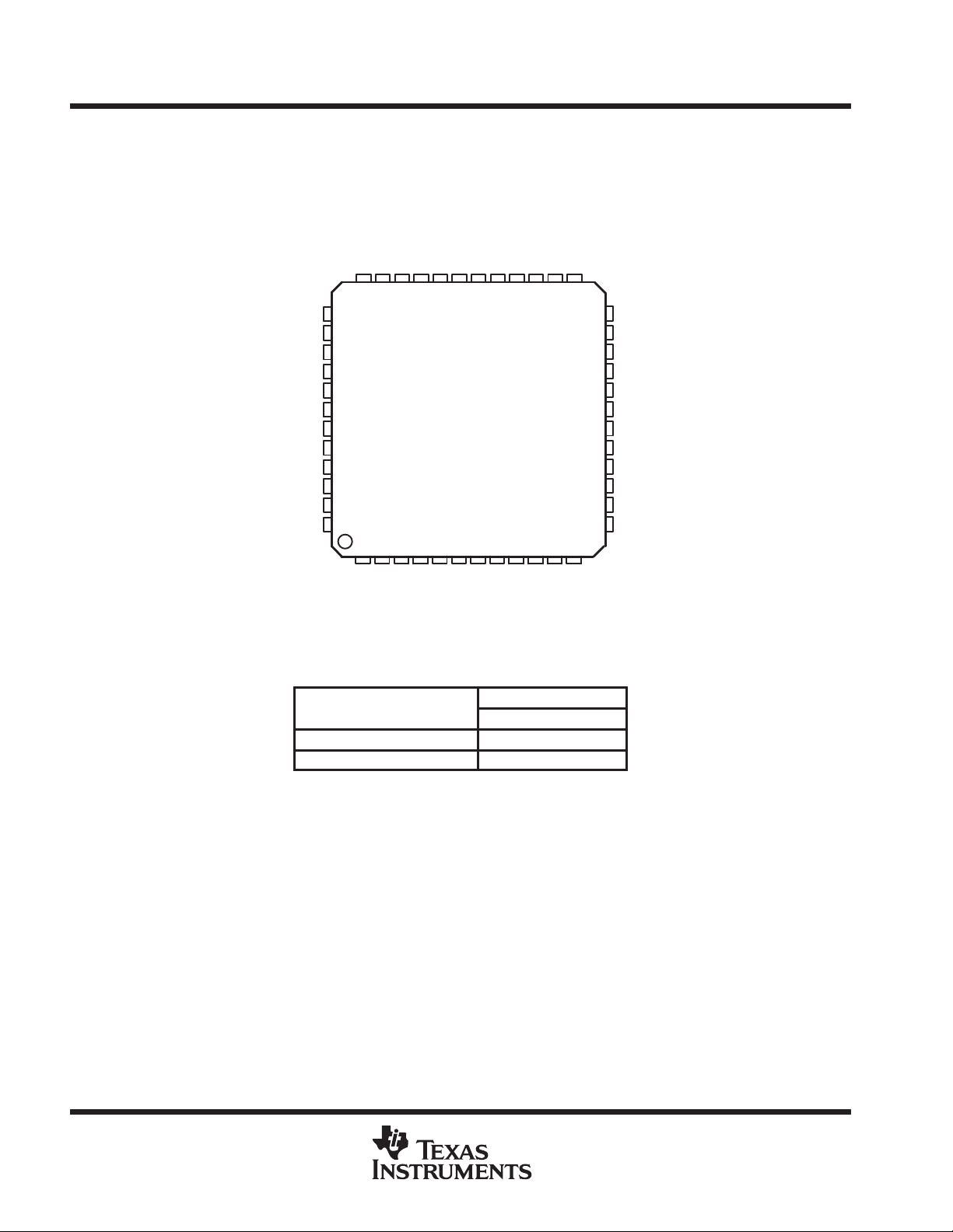
terminal assignments
LINEOUTR
LINEOUTL
CX3D2
CX3D1
PFB PACKAGE
(TOP VIEW)
CAP1
MODE0
AFILT1
CAP2
SS1
VREFOUT
VREF
AV
DD1
AV
MONOOUT
AV
DD2
LNLVLOUTL
MODE1
LNLVLOUTR
AV
SS2
GPIO
GPIO
CID0
CID1
EAPD
GPIO
35 34 33 32 3136 30
37
38
39
40
41
42
43
44
45
46
47
48
23
1
DD1
XTLIN
DV
5678
4
SS1
DV
XTLOUT
SS2
DV
BITCLK
28 27 2629
9
SDATAIN
10 11 12
DD2
SYNC
DV
25
RESETB
SDATAOUT
ORDERING INFORMATION
A
0°C to 70°C TLV320AIC27CPFB
–40°C to 85°C TLV320AIC27IPFB
PACKAGE
48-TQFP PFB
LINEINR
24
LINEINL
23
MIC2
22
21
MIC1
20
CDR
CDGND
19
CDL
18
VIDEOR
17
VIDEOL
16
AUXR
15
AUXL
14
PHONE
13
PCBEEP
2
POST OFFICE BOX 655303 • DALLAS, TEXAS 75265
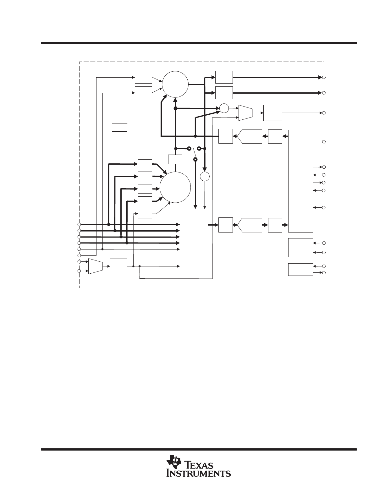
functional block diagram—two-channel mode
TLV320AIC27
STEREO AUDIO CODEC
SLAS253 – MARCH 2000
CD (18,20)
LINEIN (23,24)
VIDEO (16,17)
AUX (14,15)
PHONE (13)
PCBEEP (12)
MIC[1] (21)
MIC[2] (22)
MUX
KEY:
0dB/
20dB
VOL/
MUTE
VOL/
MUTE
MONO
STEREO
VOL/
MUTE
VOL/
MUTE
VOL/
MUTE
VOL/
MUTE
VOL/
MUTE
∑
3D
∑
RECORD
MUX
AND
MUTE
VOL/
MUTE
VOL/
MUTE
∑
MUX
VOL
∑
VOL
STEREO
DAC
STEREO
DAC
VOL/
MUTE
SRC
SERIAL
I/F
SRC
MASTER/
SLAVE
SELECT
OSC
(35,36)
LINEOUT
(39,41)
LNLVLOUT
(37)
MONOOUT
(47) EAPD
(6) BITCLK
(10) SYNC
(8)
SDATAIN
(5)
SDATAOUT
(11)
RESETB
(45)CID[0]
(46)CID[1]
(2) XTLIN
(3) XTLOUT
POST OFFICE BOX 655303 • DALLAS, TEXAS 75265
3
TLV320AIC27
STEREO AUDIO CODEC
SLAS253 – MARCH 2000
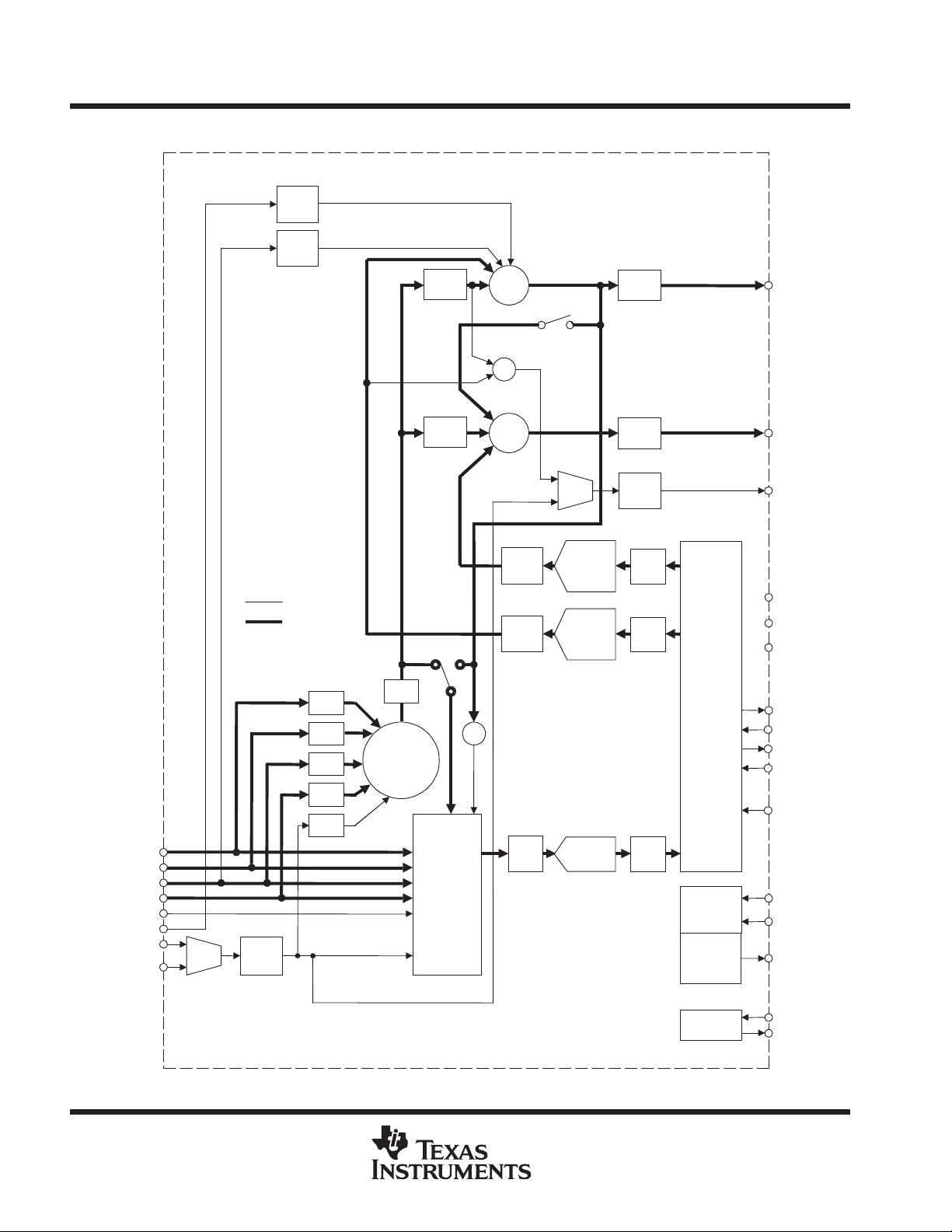
functional block diagram—6-channel I2S, quad, and modem modes
VOL/
MUTE
VOL/
MUTE
VOL/
MUTE
∑
∑
REV . 2.1
SWITCH
VOL/
MUTE
(35,36)
LINEOUT
(FRONT)
CD (18,20)
LINEIN (23,24)
VIDEO (16,17)
AUX (14,15)
PHONE (13)
PCBEEP (12)
MIC[1] (21)
MIC[2] (22)
MUX
KEY:
0dB/
20dB
MONO
STEREO
VOL/
MUTE
VOL/
MUTE
VOL/
MUTE
VOL/
MUTE
VOL/
MUTE
3D
∑
VOL/
MUTE
RECORD
MUX
AND
MUTE
∑
MUX
VOL/
MUTE
VOL/
MUTE
∑
VOL
REAR
STEREO
DAC
FRONT
STEREO
DAC
STEREO
ADC
VOL/
MUTE
VOL/
MUTE
SRC
SRC
SRC
SERIAL
I/F
MASTER/
SLAVE
SELECT
General
Supprt GPIO[1:3]
(39,41)
LINEOUT
(REAR)
(37)
MONOOUT
(40) MODE1
(30) MODE0
(47) EAPD
(6) BITCLK
(10) SYNC
(8)
SDATAIN
(5)
SDATAOUT
(11)
RESETB
(45)CID[0]
(46)CID[1]
(43,44,48)IO
OSC
4
POST OFFICE BOX 655303 • DALLAS, TEXAS 75265
(2) XTLIN
(3) XTLOUT
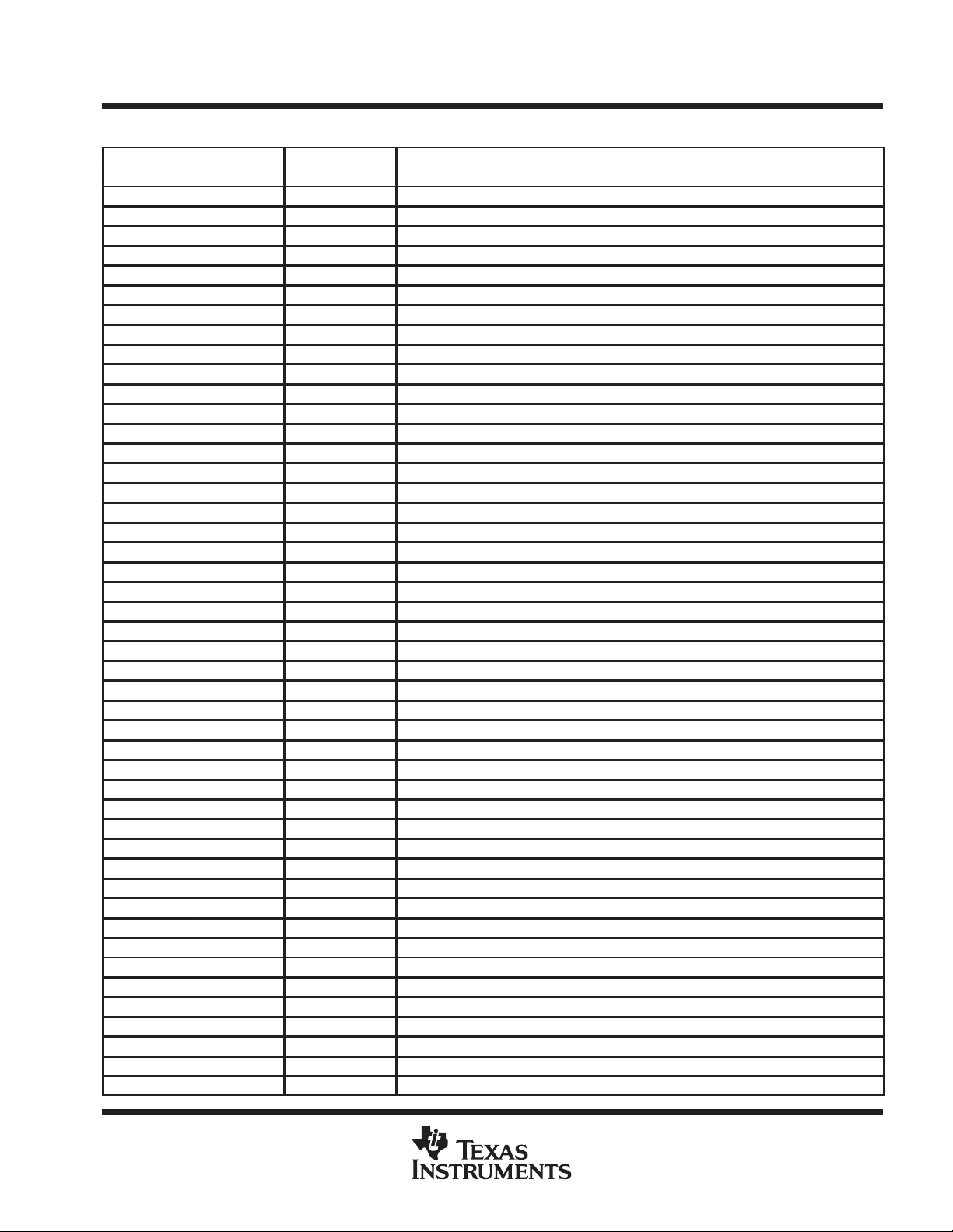
TYPE
DESCRIPTION
STEREO AUDIO CODEC
Terminal Functions
TERMINAL
NAME NO.
AFILT1 29 Analog output Buffered CAP2. This terminal has an internal connection.
VIDEOL 16 Analog input Mixer input, typically for VIDEO signal
VIDEOR 17 Analog input Mixer input, typically for VIDEO signal
AUXL 14 Analog input Mixer input, typically for AUX signal
AUXR 15 Analog input Mixer input, typically for AUX signal
AV
DD1
AV
DD2
AV
SS1
AV
SS2
BITCLK 6 Digital output Serial interface clock output to AC’97 controller
CAP1 31 Analog output Buffered CAP2. This terminal has an internal connection.
CAP2 32 Analog input Reference input/output; pulls to midrail if not driven
CDGND 19 Analog input CD input common-mode reference (ground)
CDL 18 Analog input Mixer input, typically for CD signal
CDR 20 Analog input Mixer input, typically for CD signal
CID0 45 Digital input Master/slave ID select (internal pullup)
CID1 46 Digital input Master/slave ID select (internal pullup)
CX3D1 33 Analog output Output pin for 3D difference signal
CX3D2 34 Analog input Input pin for 3D difference signal
DV
DD1
DV
DD2
DV
SS1
DV
SS2
EAPD 47 Digital output External amplifier power down/GPO
GPIO 43, 44, 48 General-purpose I/O
LINEINL 23 Analog input Mixer input, typically for LINE signal
LINEINR 24 Analog input Mixer input, typically for LINE signal
LINEOUTL 35 Analog output Main analog output for left channel
LINEOUTR 36 Analog output Main analog output for right channel
LNLVLOUTL 39 Analog output Left channel line-level output
LNLVLOUTR 41 Analog output Right channel line-level output
MIC1 21 Analog input Mixer input with extra gain, if required
MIC2 22 Analog input Mixer input with extra gain, if required
MONOOUT 37 Analog output Main mono output
MODE0 30 Digital input Mode select pin, internal pulldown
MODE1 40 Digital input Mode select pin, internal pulldown
PCBEEP 12 Analog input Mixer input, typically for PCBEEP signal
PHONE 13 Analog input Mixer input, typically for PHONE signal
RESETB 11 Digital input NOT reset input (active low, resets registers)
SDATAIN 8 Digital output Serial-data output to AC’97 controller
SDATAOUT 5 Digital input Serial-data input
SYNC 10 Digital input Serial-interface sync pulse from AC’97 controller
VREF 27 Analog output Buffered CAP2. This terminal has an internal connection.
VREFOUT 28 Analog output Reference for microphones; buffered CAP2
XTLIN 2 Digital input Clock-crystal connection or clock input (XTAL not used)
XTLOUT 3 Digital output Clock-crystal connection
25 Supply Analog positive supply
38 Supply Analog positive supply
26 Supply Analog ground supply, chip substrate
42 Supply Analog ground supply, chip substrate
1 Supply Digital positive supply
9 Supply Digital positive supply
4 Supply Digital ground supply
7 Supply Digital ground supply
TLV320AIC27
SLAS253 – MARCH 2000
POST OFFICE BOX 655303 • DALLAS, TEXAS 75265
5
TLV320AIC27
STEREO AUDIO CODEC
SLAS253 – MARCH 2000
absolute maximum ratings over operating free-air temperature (unless otherwise noted)
†
Digital supply voltage –0.3 V to 7 V. . . . . . . . . . . . . . . . . . . . . . . . . . . . . . . . . . . . . . . . . . . . . . . . . . . . . . . . . . . . . .
Analog supply voltage –0.3 V to 7 V. . . . . . . . . . . . . . . . . . . . . . . . . . . . . . . . . . . . . . . . . . . . . . . . . . . . . . . . . . . . . .
Voltage range digital inputs DV
Voltage range analog inputs AV
SS
DD
–0.3 V to DVDD +0.3 V. . . . . . . . . . . . . . . . . . . . . . . . . . . . . . . . . . . . . . . . . . . .
–0.3 V to AVDD +0.3 V. . . . . . . . . . . . . . . . . . . . . . . . . . . . . . . . . . . . . . . . . . .
Operating temperature range, TA 0°C to 70°C. . . . . . . . . . . . . . . . . . . . . . . . . . . . . . . . . . . . . . . . . . . . . . . . . . . . .
Storage temperature –65°C to 150°C. . . . . . . . . . . . . . . . . . . . . . . . . . . . . . . . . . . . . . . . . . . . . . . . . . . . . . . . . . . . .
Lead temperature (soldering 10 seconds) 260°C. . . . . . . . . . . . . . . . . . . . . . . . . . . . . . . . . . . . . . . . . . . . . . . . . . .
Lead temperature (soldering 2 minutes) 183°C. . . . . . . . . . . . . . . . . . . . . . . . . . . . . . . . . . . . . . . . . . . . . . . . . . . . .
†
Stresses beyond those listed under “absolute maximum ratings” may cause permanent damage to the device. These are stress ratings only, and
functional operation of the device at these or any other conditions beyond those indicated under “recommended operating conditions” is not
implied. Exposure to absolute-maximum-rated conditions for extended periods may affect device reliability.
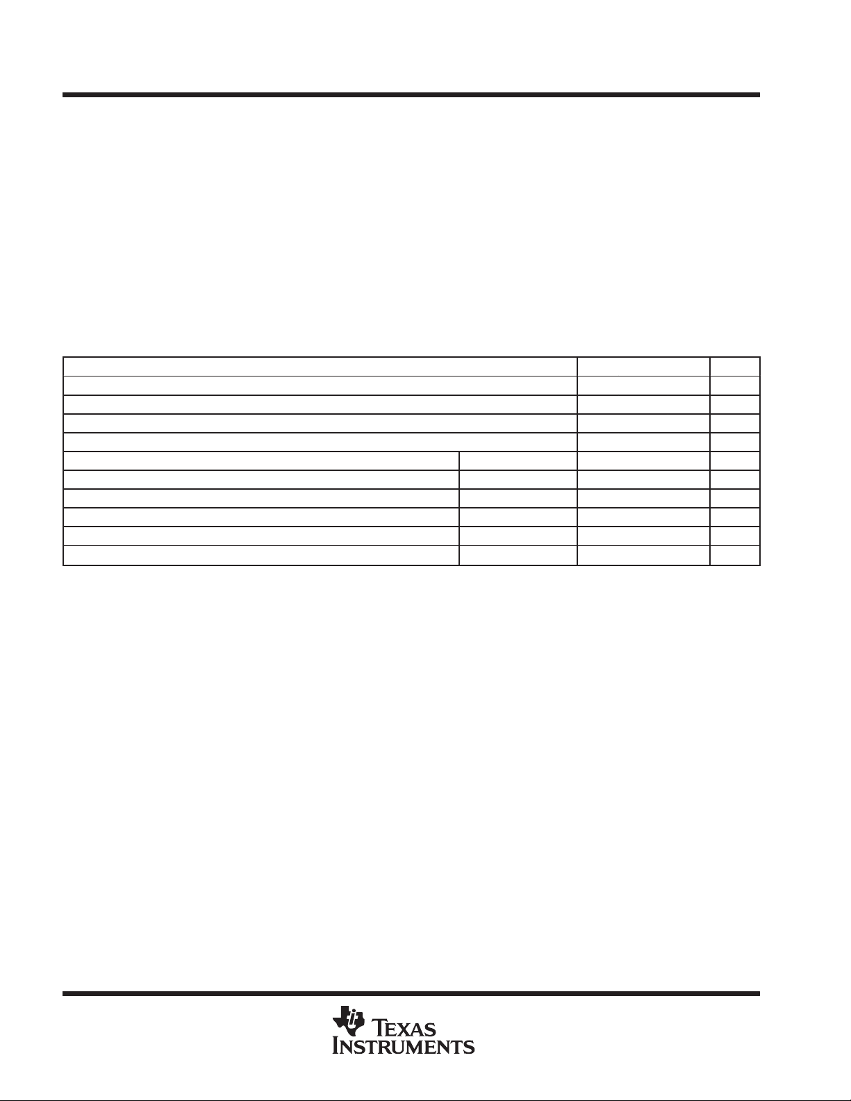
recommended operating conditions
MIN TYP MAX UNIT
Digital supply range, DV
Analog supply range, AV
Digital ground, DV
Analog ground, AV
Analog supply current DVDD, AVDD = 5 V 35 50 mA
Digital supply current DVDD, AVDD = 5 V 30 50 mA
Standby supply current (all PRs set) DVDD, AVDD = 5 V 150 600 µA
Analog supply current DVDD, AVDD = 3.3 V 22 33 mA
Digital supply current DVDD, AVDD = 3.3 V 20 22 mA
Standby supply current (all PRs set) DVDD, AVDD = 3.3 V 100 150 µA
DD
DD
SS
SS
3.3 to 5 V
3.3 to 5 V
0 V
0 V
6
POST OFFICE BOX 655303 • DALLAS, TEXAS 75265
TLV320AIC27
STEREO AUDIO CODEC
SLAS253 – MARCH 2000
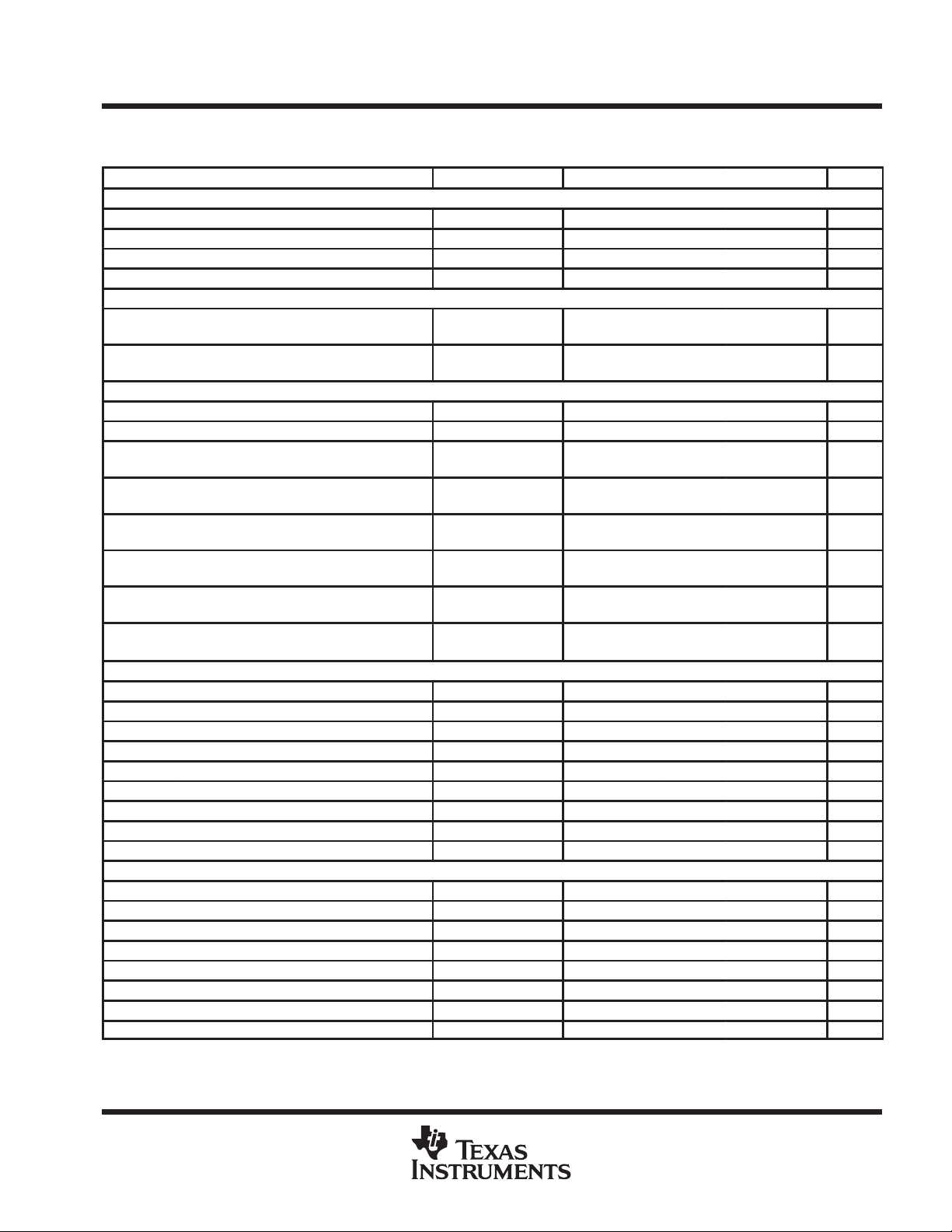
electrical characteristics, A VDD = 5 V , DVDD = 3.3 V , GND = 0 V, TA = 0°C to 70°C (unless otherwise
noted)
PARAMETER TEST CONDITIONS MIN TYP MAX UNIT
Digital Logic Levels (DVDD = 3.3 V or 5 V)
V
IL
V
IH
V
OL
V
OH
Analog I/O Levels (input signals on any inputs, outputs on LINEOUT L, R, and MONOOUT)
Reference Levels
CAP2 Reference input/output 2/5 AV
VREF Mixer reference
VREFOUT MIC reference
CAP1 ADC reference
AFILT1 DAC reference
DAC Circuit Specifications (AVDD = 5 V) 48-kHz sampling
ADC Circuit Specifications (AVDD = 5 V) 48-kHz sampling
NOTE 1: SNR is the ratio of 0-dB signal output level to the output level with no signal, measured A-weighted over a 20 Hz to 20 kHz bandwidth.
Input low level AVSS – 0.3 0.8 V
Input high level 2.2 AVDD + 0.3 V
Output low 0.1 × DV
Output high 0.9 × DV
Input level
Output level Into 10 kΩ load AVSS +100 mV
CAP2 impedance 75 kΩ
VREF current source (pins CAP1, AFILT2,
VREF and VREFOUT)
VREF current source (pins CAP1, AFILT1,
VREF and VREFOUT)
SNR A-weighted (see Note 1) 85 95 dB
Full-scale output voltage VREF = 2.5 V 1 Vrms
THD –3-dB full-scale input 74 96 dB
Frequency response 20 19200 Hz
Transition band 19200 28800 Hz
Stop band 28800 Hz
Out of band rejection –40 dB
Spurious-tone reduction –100 dB
PSRR 20 Hz to 20 kHz 40 dB
SNR A-weighted (see Note 1) 75 90 dB
ADC input for full-scale output VREF = 2.5 V 1 Vrms
THD –6-dB voltage input 80 95 dB
Frequency response 20 19200 Hz
Transition band 19200 28800 Hz
Stop band 28800 Hz
Stop-band rejection –74 dB
PSRR 20 Hz to 20 kHz 40 dB
Minimum input
impedance = 10 kΩ
AVDD = 3 V 5 15 mA
AVDD = 5 V 3 5 mA
AVSS –100 mV AVDD +100 mV V
DD
Near rail
to rail
AVDD/2 3/5 AV
DD
Buffered
CAP2
Buffered
CAP2
Buffered
CAP2
Buffered
CAP2
AVDD –100 mV V
DD
DD
V
V
V
V
V
V
V
POST OFFICE BOX 655303 • DALLAS, TEXAS 75265
7
TLV320AIC27
Input impedance (other mixer inputs)
kΩ
Input impedance mic inputs
kΩ
STEREO AUDIO CODEC
SLAS253 – MARCH 2000
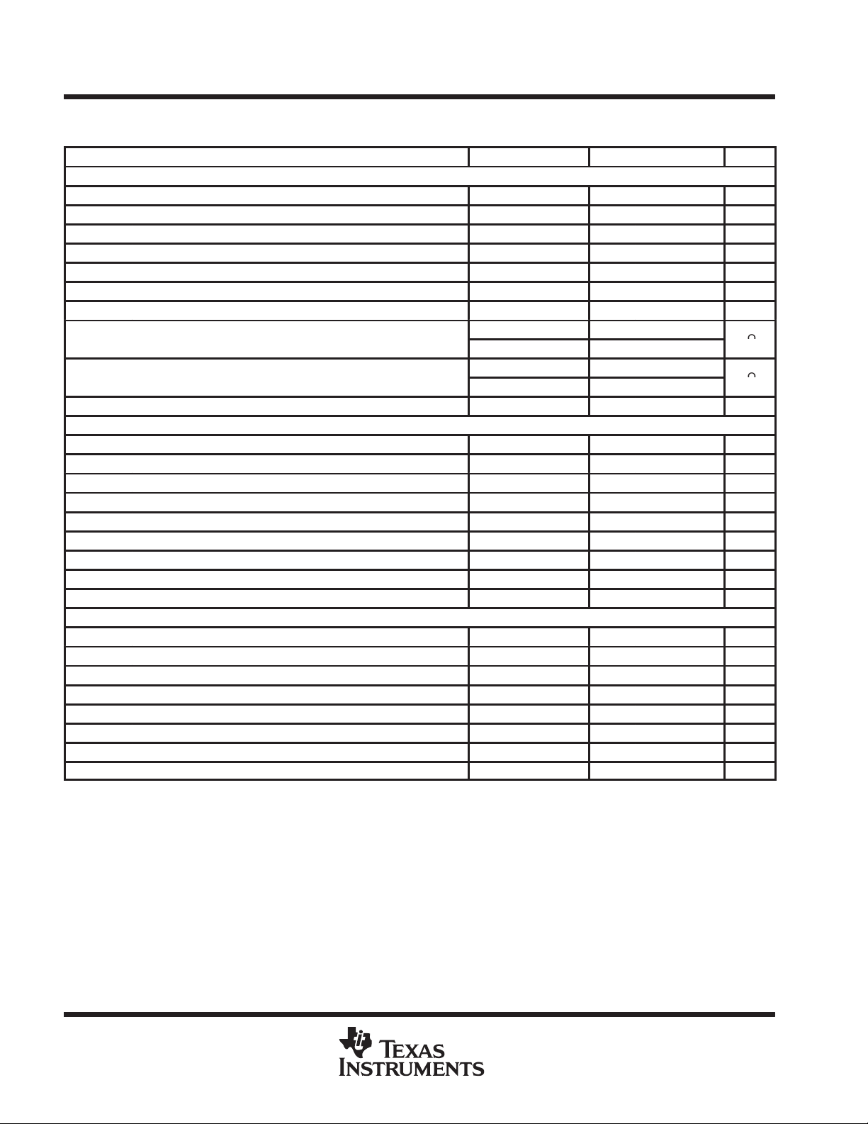
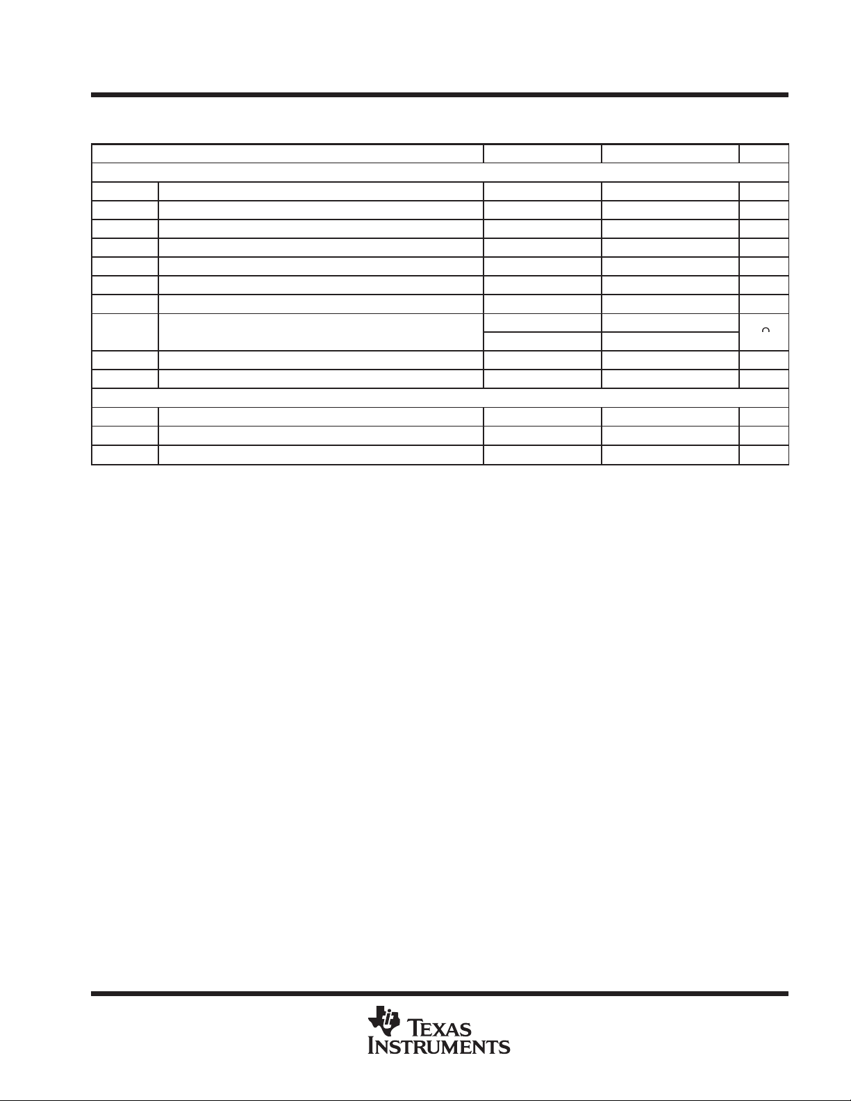
electrical characteristics, A VDD = 5 V , DVDD = 3.3 V , GND = 0 V, TA = 0°C to 70°C (unless otherwise
noted) (continued)
PARAMETER TEST CONDITIONS MIN TYP MAX UNIT
Mixer Circuit Specifications (AVDD = 5 V) 48-kHz sampling
SNR CD path A-weighted (see Note 1) 90 95 dB
SNR other paths A-weighted (see Note 1) 85 95 dB
Maximum input voltage AV
Maximum output voltage on LINEOUT 1.0 1.8 Vrms
THD 0-dB voltage input 74 90 dB
Frequency response (±1 dB) 20 20000 Hz
Input impedance (CD inputs) At any gain 15 kΩ
p
p
p
p
PSRR 20 Hz to 20kHz 40 dB
DAC Circuit Specifications (AVDD = 3.3 V) 48-kHz sampling
SNR A-weighted (see Note 1) 96 dB
Full scale output voltage VREF = 1.65 V 0.7 Vrms
THD –3-dB full-scale input 66 90 dB
Frequency response 20 Hz
Transition band 19200 19200 Hz
Stop band 28800 28800 Hz
Out-of-band rejection –40 dB
Spurious-tone reduction –100 dB
PSRR 20 Hz to 20 kHz 40 dB
ADC-Circuit Specifications (AVDD = 3.3 V) 48-kHz sampling
SNR A-weighted (see Note 1) 85 dB
ADC input for full-scale output VREF = 1.65 V 0.7 Vrms
THD –6-dB voltage input 74 80 dB
Frequency response 20 19200 Hz
Transition band 19200 28800 Hz
Stop band 28800 Hz
Stop-band rejection –74 dB
PSRR 20 Hz to 20 kHz 40 dB
NOTE 1: SNR is the ratio of 0-dB signal output level to the output level with no signal, measured A-weighted over a 20 Hz to 20 kHz bandwidth.
p
p
At maximum gain 10 20 30
At 0-db gain 50 100 150
At maximum gain 10 20 30
At 0-db gain 55 110 165
SS
1 AV
DD
Vrms
8
POST OFFICE BOX 655303 • DALLAS, TEXAS 75265
Input impedance (other mixer inputs)
kΩ
TLV320AIC27
STEREO AUDIO CODEC
SLAS253 – MARCH 2000
electrical characteristics, A VDD = 5 V , DVDD = 3.3 V , GND = 0 V, TA = 0°C to 70°C (unless otherwise
noted) (continued)
PARAMETER TEST CONDITIONS MIN TYP MAX UNIT
Mixer-Circuit Specifications (AVDD = 3.3 V) 48 kHz sampling
SNR CD path A-weighted (see Note 1) 92 dB
SNR other paths A-weighted (see Note 1) 92 dB
Maximum input voltage 0.66 Vrms
Maximum output voltage on LINEOUT 0.66 Vrms
THD 0-dB voltage input 74 90 dB
Frequency response (±1 dB) 20 20000 Hz
Input impedance (CD inputs) At any gain 15 kΩ
p
p
Input impedance mic inputs At any gain 30 kΩ
PSRR 20 Hz to 20 kHz 40 dB
Clock-Frequency Range
Crystal clock 24.576 MHz
BIT_CLK frequency 12.288 MHz
SYNC frequency 48.0 kHz
NOTE 1: SNR is the ratio of 0-dB signal output level to the output level with no signal, measured A-weighted over a 20 Hz to 20 kHz bandwidth.
p
At maximum gain 20
At 0-dB gain 100
POST OFFICE BOX 655303 • DALLAS, TEXAS 75265
9

TLV320AIC27
STEREO AUDIO CODEC
SLAS253 – MARCH 2000
detailed description
3D stereo enhancement
This device contains a stereo-enhancement circuit, designed to optimize the listening experience when the
device is used in a typical PC-operating environment (that is, with a pair of speakers placed either side of the
monitor with little spatial separation). This circuit creates a differential signal by subtracting left and right channel
playback data, then filters this difference signal using low-pass and high-pass filters whose time constants are
set using external capacitors connected to the CX3D pins 33 and 34. Typical values of 100 nF and 47 nF set
high-pass and low-pass poles at about 100 Hz and 1 kHz respectively . This frequency band corresponds to the
range over which the ear is most sensitive to directional effects.
The filtered difference signal is gain-adjusted by an amount set using the four-bit value written to register 22h
bits 3 to 0. Value 0h is disabled, and value Fh is maximum effect. A typical value of 8h is optimum. The user
interface most typically uses a slider type of control to allow the user to adjust the level of enhancement to suit
the program material. Bit D13 3D in register 20h is the overall 3D-enable bit. The capability register 00h reads
back the value 1 1000 in bits D14 to D10. This corresponds to decimal 24, which is registered with Intel as T exas
Instruments Stereo Enhancement.
Note that the external capacitors setting the filtering poles applied to the difference signal can be adjusted in
value, or even replaced with a direct connection between the pins. When such adjustments are made, the
amount of difference signal fed back into the main signal paths can be significant. This can cause large signals
which may limit, distort, or overdrive signal paths or speakers. Adjust these values carefully to select the desired
acoustic effect.
There is no provision for pseudo-stereo effects. Mono signals have no enhancement applied if they are in phase
and have the same amplitude.
Signals from the PCM DAC channels do not have stereo enhancement applied. It is assumed that these signals
have already been processed digitally with any required 3D-enhancement effect. Applying the analog
3D-enhancement will corrupt the digital effect. This is equivalent to setting the POP bit in register 20h. As a
result, the readback value of this bit is fixed as 1, and attempts to change it will be ignored. The POP bit is set
to one and cannot be reset.
variable sample rate support
The DACs and ADCs on this device support all the recommended sample rates specified in the Intel Revision
2.1 specification for both audio and modem rates. Default rates are 48 ksps. If alternative rates are selected,
the AC’97 interface continues to run at 48 kw/s (kilowords per second), but data is transferred across the link
in bursts such that the net sample rate selected is achieved. It is up to the AC’97 Revision 2.1-compliant
controller to ensure that data is supplied to the ac link, and received from the ac link at the appropriate rate.
The device supports on-demand sampling. That is, when the DAC signal-processing circuits need another
sample a request is sent to the controller, which must respond with a data sample in the next frame it sends.
For example, if a rate of 24 ksps is selected, on average the device requests a sample from the controller every
other frame, for each of the stereo DACs. Note that if an unsupported rate is written to one of the rate registers,
the rate defaults to the nearest rate supported. The register then responds when interrogated with the supported
rate the device has defaulted to.
10
POST OFFICE BOX 655303 • DALLAS, TEXAS 75265
TLV320AIC27
STEREO AUDIO CODEC
SLAS253 – MARCH 2000
variable sample rate support (continued)
ADCs are controlled similarly but with one difference: normally the left and right-channel ADCs sample at the
same rate.
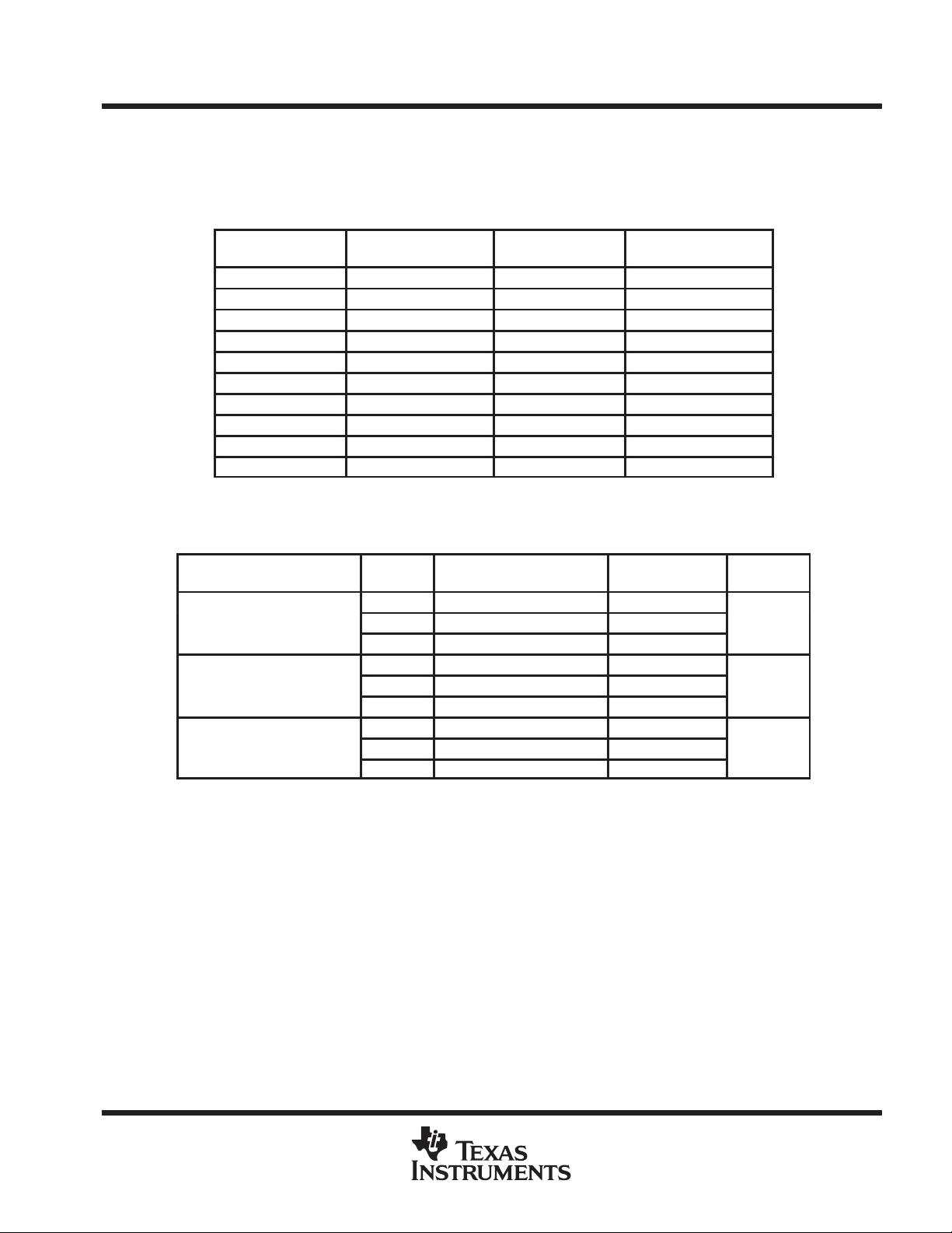
Table 1. Variable Sample Rates Supported
AUDIO
SAMPLE RATE
8000 1F40 7200 1C20
11025 2B11 8228.57 (57600/7) 2024
16000 3E80 8400 20D0
22050 5622 9000 2328
44100 AC44 9600 2580
48000 BB80 10285.71 (72000/7) 282D
CONTROL VALUE
D15–D0
MODEM
SAMPLE RATE
12000 2EE0
13714.28 (96000/7) 3592
19200 4B00
24000 5DC0
CONTROL VALUE
D15–D0
Table 2 shows which registers control which DAC rates, versus mode and ID selected.
Table 2. Variable Rate Register Location Versus Mode and ID
MODE ID
Rev 2.1 mode (00)
Rev 2.1 6-channel mode (01)
Quad mode (10)
FRONT DAC RATE
REGISTER
00 and 01 2Ch
10 2Eh
11 2Ch (center) and 30h (LFE)
00 and 01 2Ch
10 2Eh
11 2Ch (center) and 30h (LFE)
00 and 01 2Ch 2Eh
10 2Eh 2Ch
11 2Ch (center) and 30h (LFE) 2Eh
REAR DAC RATE
REGISTER
ADC RATE
REG
32h
32h
32h
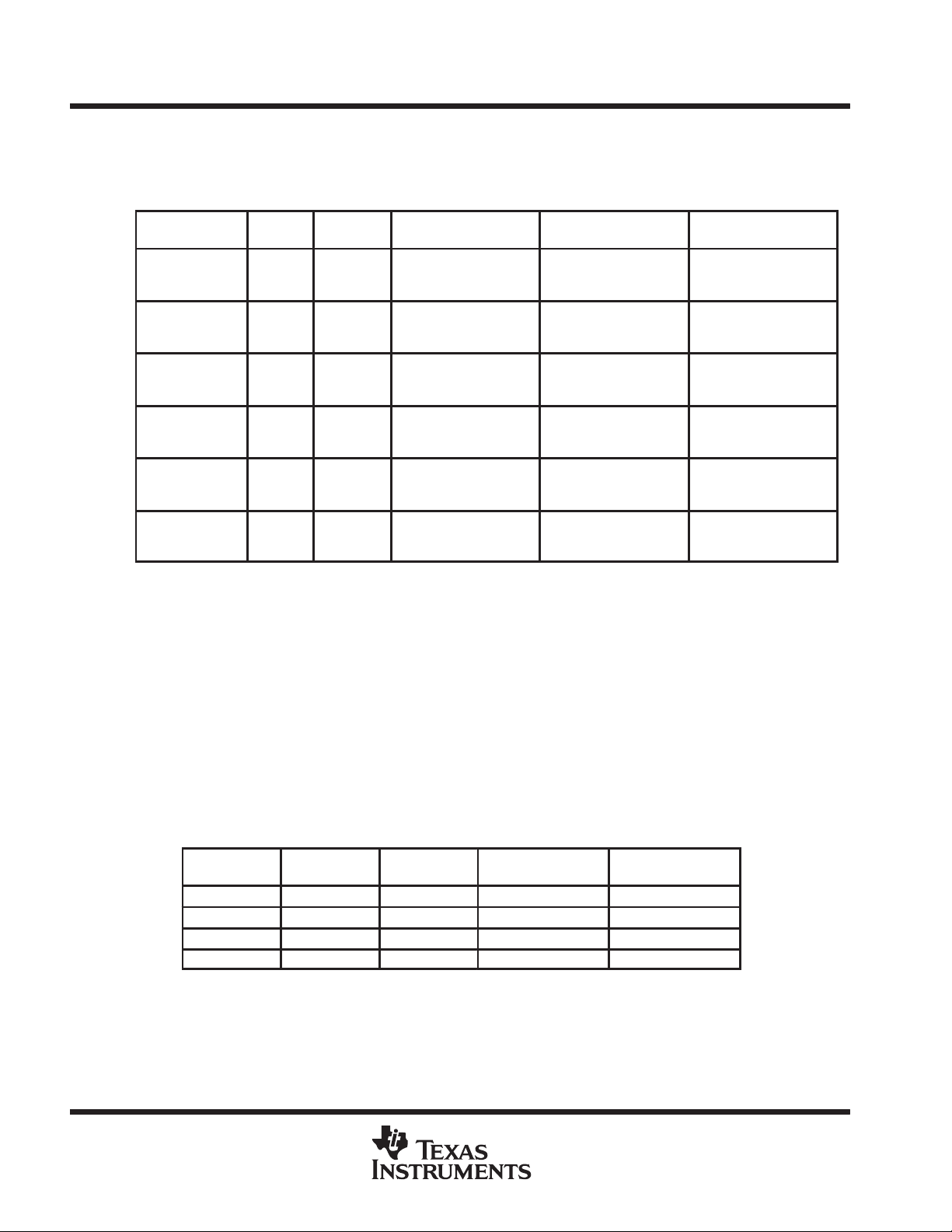
gain control register location versus mode and ID
Depending on the operational mode and ID of the device, the various gain control registers have locations in
the register map that may change. For example, if the codec is configured as ID 10, it means that the device
will be converting the rear surround DAC data. In this case, the surround DAC volume word written to register
38h is now used to control the master volume control, rather than the normal master volume 02h. In addition,
when the surround volume mute control is written as demute, mute in the DAC PGA register 18h is automatically
overridden. Then the user does not have to make an unexpected additional write to register 18h to demute the
DAC PGA.
POST OFFICE BOX 655303 • DALLAS, TEXAS 75265
11
TLV320AIC27
STEREO AUDIO CODEC
SLAS253 – MARCH 2000
gain control register location versus mode and ID (continued)
Table 3. Gain Control Register Location Versus Mode and ID
PGA
Front DAC PGA
Rear DAC PGA
Front mixer
Rear mixer
Front volume
Rear volume
CODECIDCONTROL
0x
10
11
0x
10
11
0x
10
11
0x
10
11
0x
10
11
0x
10
11
REG
18h
70h
72h Not muted (bit 15) Not muted (bit 15) Not muted (bit 15)
74h Permanently muted Not muted (bit 15) Permanently muted
02h
38h
36h
04h
REV 2.1 MODE (0x)
MUTE DEFAULT
Muted (bit 15)
AND with 38h, 7, 15
AND with 36h, 7, 15
Muted (bit 15) and
powered off
Muted (bit 15)
Muted (7 and 15)
Muted (7 and 15)
Muted (bit 15) Rev 2.1
switch enabled
QUAD MODE (10)
MUTE DEFAULT
Muted (bit 15)
AND with 38h, 7, 15
AND with 36h, 7, 15
Not muted (bit 15)
AND with 02h, 15
AND with 38h, 7, 15
Muted (bit 15)
Muted (7 and 15)
Muted (7 and 15)
Muted (7 and 15)
Muted (bit 15)
Muted (7 and 15)
MODEM MODE (11)
Muted (bit 15)
AND with 38h, 7, 15
AND with 36h, 7, 15
AND with 04h, 15
Muted (bit 15)
Muted (7 and 15)
Muted (7 and 15)
Muted (bit 15)
master/slave ID0/1 support
TL V320AIC27 supports operation as either a master or a slave codec. Configuring the device as master or slave
is accomplished by tying together the CID pins CID0 and CID1 (pins 45 and 46 ).
Fundamentally , a device identified as a master (ID = 00) produces BITCLK as an output, whereas a slave (any
ID but 00) must be provided with BITCLK as an input. The obvious implication is that if the master device on
an ac link is disabled, the slave devices cannot function.
The AC’97 Revision 2.1 specification defines the CID pins as having inverting sense and being provided with
internal weak pull ups. Therefore, if no connections are made to the CID0/1 pins, then these pins pull hi and
an ID = 00 (or master) is selected. External connections to ground select other IDs.
Table 4. ID Selection
PIN 45 CID0 PIN 46 CID1 ID SELECTED
NC NC 00 Master Output
NC Ground 01 Slave Input
Ground NC 10 Slave Input
Ground Ground 11 Slave Input
MASTER OR
SLAVE
BITCLK
12
POST OFFICE BOX 655303 • DALLAS, TEXAS 75265
6-channel (01)
TLV320AIC27
STEREO AUDIO CODEC
SLAS253 – MARCH 2000
master/slave ID0/1 support (continued)
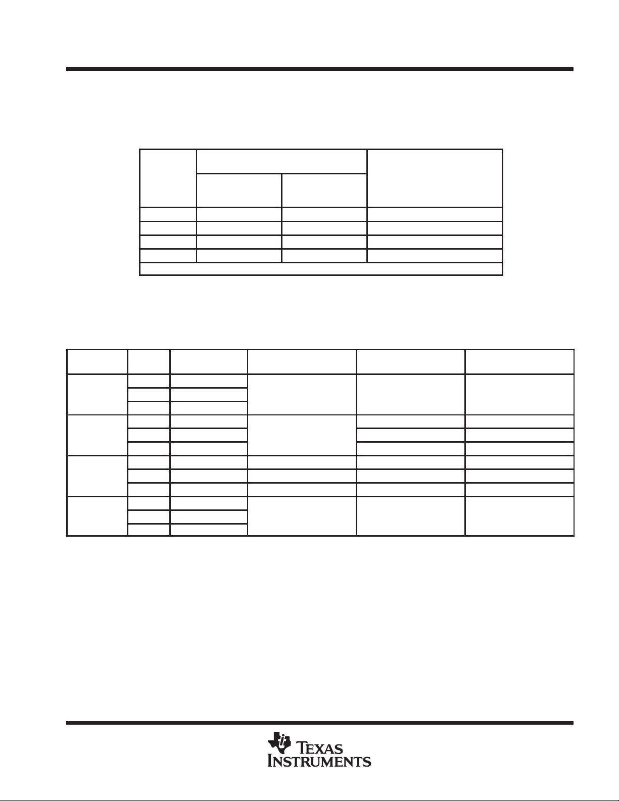
The TL V320AIC27 supports the AMAP function, whereby selection of an ID automatically maps the data from
the interface onto the PCM DACs.
Table 5. Default Slot to DAC Mappings Based on Codec ID
AC-LINK FRAME DATA
USED FOR DACs
CODEC ID
00 3 4 Original definition (master)
01 3 4 Original definition (docking)
10 7 8 Left/right surround channels
11 6 9 Center/LFE channels
The codec ID is available to the controller via register 28h and C3, bits D15 and D14
PCM LEFT DAC
USES DATA FROM
SLOT NUMBER
PCM RIGHT DAC
USES DATA FROM
SLOT NUMBER
The previous automatic mapping of data to slots is extended when the device is operated in the alternative
modes selectable via the mode pins. In these cases the selection of which data slots are mapped onto internal
DACs or I2S outputs is accomplished as shown in Table 6. Note that I2S enable bit must be set.
COMMENTS
Table 6. Slot to DAC and Mapping Based on Mode and Codec ID
MODE
Rev 2.1 (00)
Rev 2.1
-
Quad (10)
Modem (11)
CODECIDSLOTS MAPPED
TO FRONT DACs
00 or 01 3 and 4
10 7 and 8
11 6 and 9
00 or 01 3 and 4 7 and 8 6 and 9
10 7 and 8
11 6 and 9 7 and 8 3 and 4
00 or 01 3 and 4 7 and 8 7 and 8 6 and 9
10 7 and 8 3 and 4 3 and 4 6 and 9
11 6 and 9 7 and 8 7 and 8 3 and 4
00 or 01 3 and 4
10 7 and 8
11 6 and 9
SLOTS MAPPED TO
REAR DACs
Not supported in this mode Not supported in this mode Not supported in this mode
Not supported in this mode
5 (or 5 and 10 if DLM set) Not supported in this mode Not supported in this mode
DATA TO I2S D0
PIN 44
3 and 4 6 and 9
DATA TO I2S D1
PIN 43
slave codec register access definitions
Master codec access is exactly as defined for AC’97. For slave codec access, the AC’97 digital controller must
invalidate the tag bits for slots 1 and 2 command address and data (slot 0, bits 14 and 13) and place a nonzero
value (01, 10, or 11) into the codec ID field (slot 0, bits 1 and 0).
Slave codecs disregard the command address and command data (slot 0, bits 14 and 13) tag bits when they
see a two-bit codec ID value (slot 0, bits 1 and 0) that matches their configuration. In a sense, the slave codec
ID field functions as an alternative valid command address (for slave reads and writes) and command data (for
slave writes) tag indicator.
Slave codecs must monitor the frame valid bit and ignore the frame (regardless of the state of the slave codec
ID bits) when it is not valid. AC’97 digital controllers should set the frame valid bit for a frame with a slave register
access, even if no other bits in the output tag slot, except the slave codec ID bits, are set.
POST OFFICE BOX 655303 • DALLAS, TEXAS 75265
13
TLV320AIC27
STEREO AUDIO CODEC
SLAS253 – MARCH 2000
slave codec register access definitions (continued)
Table 7. Slave Codec Register Access Slot 0 – Bit Definitions
OUTPUT TAG SLOt (16 bits)
BIT DESCRIPTION
15 Frame valid
14 Slot 1 valid command address bit (master codec only)
13 Slot 2 valid command data bit (master codec only)
12–3 Slot 3–12 valid bits as defined by AC’97
2 Reserved (set to 0)
1–0 Two-bit codec ID field (00 reserved for master; 01, 10, 11 indicate slave)
New definitions for slave codec register access
control interface
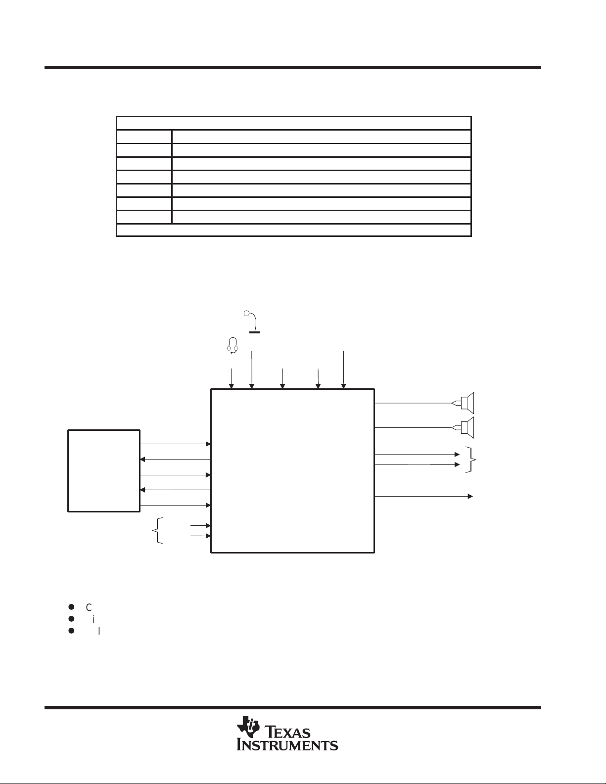
A digital interface is provided to control the TL V320AIC27 and transfer data to and from it. This serial interface
is compatible with the Intel AC’97, as illustrated in Figure 1.
system information
CD, VIDEO,
AUX, LINEINL/R
13122122
35
36
39
41
37
C54X
/C6X
OR AC’97
COMPLIANT
DIGITAL
CONTROLLER
SELECT
CHIP
RESET
BITCLK
SYNC
SDATAIN
SDATAOUT
CID0
CID1
11
6
10
8
5
45
46
MIC2
MIC1
PCBEEP PHONE
TLV320AIC27
Figure 1. Revision 2.1 Compliant Two-Channel Codec
The main control interface functions are:
D
Control of analog gain and signal paths through the mixer
D
Bidirectional transfer of ADC and DAC words to and from AC’97 controller
D
Selection of power down modes
LINEOUTL/R
LNLVLOUTL/R
MONOOUT
14
POST OFFICE BOX 655303 • DALLAS, TEXAS 75265
system information (continued)
TLV320AIC27
STEREO AUDIO CODEC
SLAS253 – MARCH 2000
TLV320AIC27
SDATAOUT
C54XX/C6X
McBSP
Or AC’97 compliant
digital controller
BITCLK
SDATAIN
SYNC
RESET
SDATAOUT
BITCLK
SDATAIN
SYNC
RESET
XTLOUT
TLV320AIC27
XTLIN
SDATAOUT
BITCLK
SDATAIN
SYNC
RESET
LINEOUTL
LINEOUTR
ID=00
LINEOUTL
LINEOUTR
ID=10
Front R data
Front L data
Surround R data
Surround L data
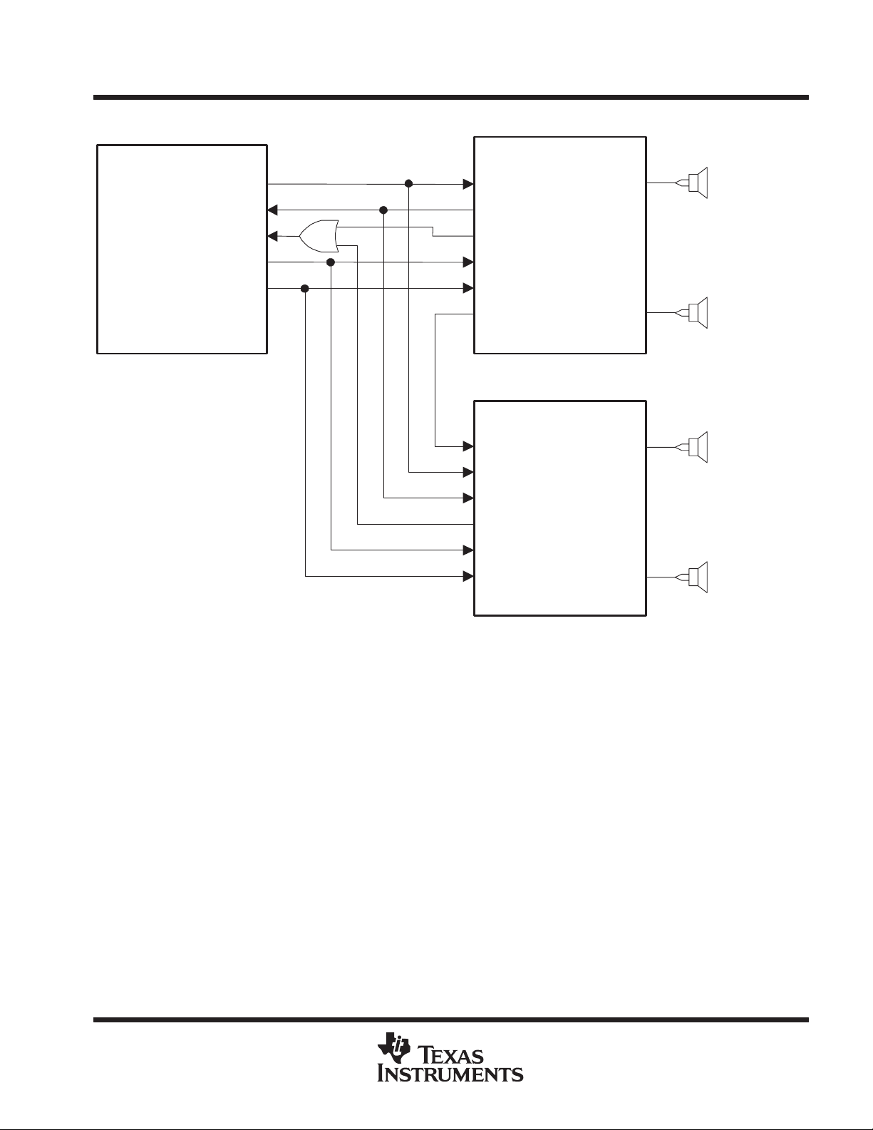
Figure 2. TLV320AIC27 In a Four-Channel System
POST OFFICE BOX 655303 • DALLAS, TEXAS 75265
15
TLV320AIC27
STEREO AUDIO CODEC
SLAS253 – MARCH 2000
system information (continued)
TLV320AIC27
C54XX
C6X
McBSP
SDATAOUT
SDATAIN
OR AC’97
COMPLIANT
DIGITAL
CONTROLLER
BITCLK
SYNC
RESET
SDATAOUT
BITCLK
SDATAIN
SYNC
RESET
XTLOUT
TLV320AIC27
XTLIN
SDATAOUT
BITCLK
SDATAIN
SYNC
RESET
TLV320AIC27
XTLIN
SDATAOUT
BITCLK
SDATAIN
SYNC
RESET
LINEOUTL
LINEOUTR
ID=00
LINEOUTL
LINEOUTR
ID=10
LINEOUTL
LINEOUTR
ID=11
Front R data
Front L data
Surround R data
Surround L data
Center data
LFE data
16
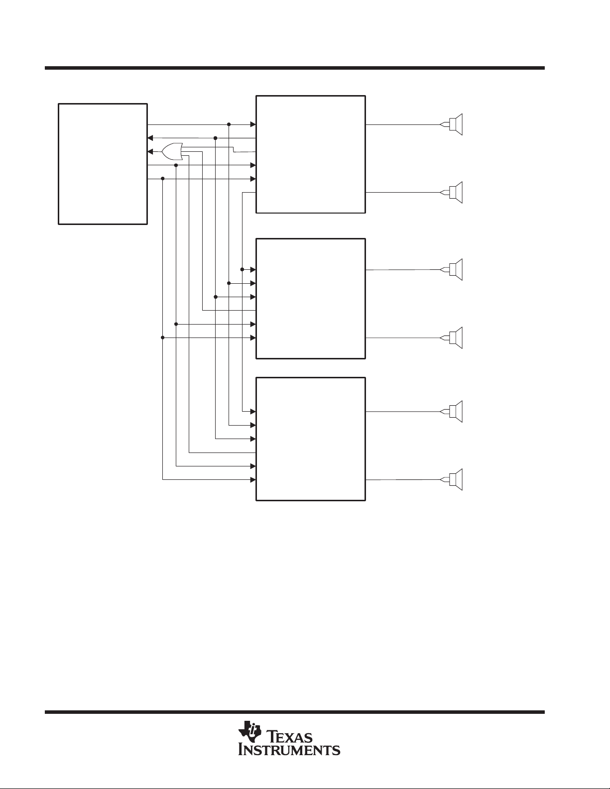
Figure 3. TLV320AIC27 In a Six-Channel System
POST OFFICE BOX 655303 • DALLAS, TEXAS 75265
 Loading...