

Page 1
SLAU229B – October 2007 – Revised August 2008
TLV320AIC12KEVMB-K and TLV320AIC14KEVMB-K User's
This user's guide describes the characteristics, operation, and use of evaluation modules
TLV320AIC12KEVMB and TLV320AIC14KEVMB, both as stand-alone and as kits
(TLV320AIC12KEVMB-K and TLV320AIC14KEVMB-K). A complete circuit description, schematic diagram
and bill of materials are also included.
The following related documents are available through the Texas Instruments web site at www.ti.com .
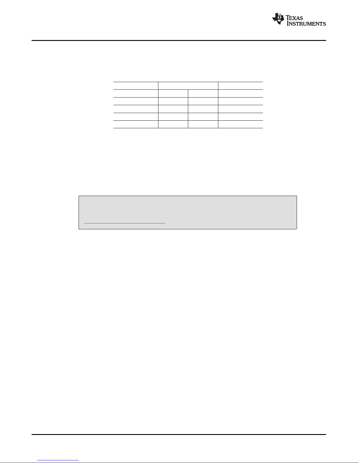
EVM-Compatible Device Data Sheets
Device Literature Number
TLV320AIC12K/14K SLWS115E
TAS1020B SLES025
REG1117-3.3 SBVS001
TPS767D318 SLVS209
SN74LVC125A SCAS290
SN74LVC1G125 SCES223
SN74LVC1G07 SCES296
User's Guide
Guide
Contents
1 EVM Overview ............................................................................................................... 3
2 Analog Interface .............................................................................................................. 3
3 Digital Interface .............................................................................................................. 4
4 Power Supplies .............................................................................................................. 6
5 EVM Operation ............................................................................................................... 6
6 Kit Operation ................................................................................................................. 7
7 EVM Bill of Materials ....................................................................................................... 29
Appendix A TLV320AIC12KEVMB/14KEVMB Schematic ................................................................. 32
Appendix B USB-MODEVM Schematic ...................................................................................... 33
List of Figures
1 TLV320AIC12KEVMB-K/14KEVMB-K Block Diagram .................................................................. 8
2 Default Software Screen .................................................................................................. 10
3 Information Tab ............................................................................................................. 12
4 Sounds and Audio Devices Properties .................................................................................. 13
5 Preset Configurations ...................................................................................................... 14
6 Device Controls Tab ....................................................................................................... 15
7 Control Register 1 Tab .................................................................................................... 16
8 Control Register 2 Tab .................................................................................................... 17
9 Control Register 3 Tab .................................................................................................... 17
10 Control Register 4 Tab .................................................................................................... 18
11 Control Register 5 Tab .................................................................................................... 18
12 Control Register 6 Tab .................................................................................................... 19
SMARTDM is a trademark of Texas Instruments.
I2C is a trademark of Koninklijke Philips Electronics N.V.
Windows is a registered trademark of Microsoft Corporation.
LabView is a trademark of National Instruments.
SLAU229B – October 2007 – Revised August 2008 TLV320AIC12KEVMB-K and TLV320AIC14KEVMB-K User's Guide 1
Submit Documentation Feedback
Page 2

www.ti.com
13 Command Line Interface Tab ............................................................................................ 20
14 File Menu .................................................................................................................... 21
15 Options Menu ............................................................................................................... 21
16 Help .......................................................................................................................... 22
List of Tables
1 Analog Interface Pinout ..................................................................................................... 3
2 Alternate Analog Connectors ............................................................................................... 4
3 Digital Interface Pinout ...................................................................................................... 4
4 Power Supply Pinout ........................................................................................................ 6
5 List of Jumpers ............................................................................................................... 7
6 USB-MODEVM SW2 Settings ............................................................................................. 9
7 USB Control Endpoint HIDSETREPORT Request .................................................................... 22
8 Data Packet Configuration ................................................................................................ 23
9 GPIO Pin Assignments .................................................................................................... 25
10 TLV320AIC12KEVMB/14KEVMB Bill of Materials ..................................................................... 29
11 USB-MODEVM Bill of Materials .......................................................................................... 30
2 TLV320AIC12KEVMB-K and TLV320AIC14KEVMB-K User's Guide SLAU229B – October 2007 – Revised August 2008
Submit Documentation Feedback
Page 3
www.ti.com
1 EVM Overview
1.1 Features
1.2 Introduction
2 Analog Interface
EVM Overview
• Full-featured evaluation board for the TLV320AIC12K/14K audio codec
• TLV320AIC12KEVMB-K/14KEVMB-K features USB connectivity for quick and easy setup.
• Intuitive evaluation software
• Easy interfacing to multiple analog sources
• Analog output signals from the TLV320AIC12K/14K are available on top and bottom connectors.
• On-board headphone jack, external microphone jack and electret microphone are included
• Digital control signals can be applied directly to top and bottom connectors.
The TLV320AIC12KEVMB-K/14KEVMB-K is a complete evaluation/demonstration kit, which includes a
USB-based motherboard called the USB-MODEVM Interface board and evaluation software for use with a
personal computer running Microsoft Windows
®
operating systems. Provisions are made for connecting all
audio inputs and outputs either from the modular connectors or with on-board terminals, a headphone
jack, and external microphone jack. An on-board electret microphone is also provided.
For maximum flexibility, the TLV320AIC12KEVMB/14KEVMB is designed for easy interfacing to multiple
analog sources. Samtec part numbers SSW-110-22-F-D-VS-K and TSM-110-01-T-DV-P provide a
convenient 10-pin dual row header/socket combination at J1 and J2. These headers/sockets provide
access to the analog input and output pins of the device. Consult Samtec at www.samtec.com or call
1-800-SAMTEC-9 for a variety of mating connector options. Table 1 summarizes the analog interface
pinout for the TLV320AIC12KEVMB/14KEVMB.
Table 1. Analog Interface Pinout
PIN NUMBER SIGNAL DESCRIPTION
J1.1 OUTM1 Inverting output of the DAC
J1.2 OUTP1 Noninverting output of the DAC
J1.3 OUTMV Programmable virtual ground for the output of OUTP2 and OUTP3
J1.4 OUTP2 Analog output number 2 from the 16- Ω driver
J1.5 OUTMV Programmable virtual ground for the output of OUTP2 and OUTP3
J1.6 OUTMV Programmable virtual ground for the output of OUTP2 and OUTP3
J1.7 OUTMV Programmable virtual ground for the output of OUTP2 and OUTP3
J1.8 OUTP2 Analog output number 3 from the 16- Ω driver
J1.9 AGND Analog Ground
J1.10 NC Not Connected
J1.11 AGND Analog Ground
J1.12 NC Not Connected
J1.13 AGND Analog Ground
J1.14 NC Not Connected
J1.15 NC Not Connected
J1.16 NC Not Connected
J1.17 AGND Analog Ground
J1.18 NC Not Connected
J1.19 AGND Analog Ground
J1.20 NC Not Connected
J2.1 INM2 Inverting analog input 2
SLAU229B – October 2007 – Revised August 2008 TLV320AIC12KEVMB-K and TLV320AIC14KEVMB-K User's Guide 3
Submit Documentation Feedback
Page 4
Digital Interface
www.ti.com
Table 1. Analog Interface Pinout (continued)
PIN NUMBER SIGNAL DESCRIPTION
J2.2 INP2 Noninverting analog input 2
J2.3 NC Not Connected
J2.4 NC Not Connected
J2.5 NC Not Connected
J2.6 NC Not Connected
J2.7 INM1 Inverting analog input 1
J2.8 INP1 Noninverting analog input 1
J2.9 AGND Analog Ground
J2.10 NC Not Connected
J2.11 AGND Analog Ground
J2.12 NC Not Connected
J2.13 AGND Analog Ground
J2.14 NC Not Connected
J2.15 NC Not Connected
J2.16 NC Not Connected
J2.17 AGND Analog Ground
J2.18 NC Not Connected
J2.19 AGND Analog Ground
J2.20 NC Not Connected
3 Digital Interface
In addition to the analog headers, the analog inputs and outputs may also be accessed through alternate
connectors, either screw terminals or audio jacks. The microphone input is also tied to J8 and the headset
output tied to J11. Table 2 summarizes the screw terminals available on the
TLV320AIC12KEVMB/14KEVMB.
Table 2. Alternate Analog Connectors
DESIGNATOR PIN 1 PIN 2 PIN3
J6 OUTP1 OUTM1
J7 OUTP2 OUTMV OUTP3
J9 INP2 INM2
J10 INM1 INP1
The TLV320AIC12KEVMB/14KEVMB is designed to easily interface with multiple control platforms.
Samtec part numbers SSW-110-22-F-D-VS-K and TSM-110-01-T-DV-P provide a convenient 10-pin dual
row header/socket combination at J4 and J5. These headers/sockets provide access to the digital control
and serial data pins of the device. Consult Samtec at www.samtec.com or call 1-800- SAMTEC-9 for a
variety of mating connector options. Table 3 summarizes the digital interface pinout for the
TLV320AIC12KEVMB/14KEVMB.
Table 3. Digital Interface Pinout
PIN NUMBER SIGNAL DESCRIPTION
J4.1 NC Not Connected
J4.2 NC Not Connected
J4.3 NC Not Connected
J4.4 DGND Digital Ground
J4.5 NC Not Connected
TLV320AIC12KEVMB-K and TLV320AIC14KEVMB-K User's Guide4 SLAU229B – October 2007 – Revised August 2008
Submit Documentation Feedback
Page 5
www.ti.com
Digital Interface
Table 3. Digital Interface Pinout (continued)
PIN NUMBER SIGNAL DESCRIPTION
J4.6 NC Not Connected
J4.7 NC Not Connected
J4.8 AIC12K/14K RESET Reset signal input to AIC12K/14KEVMB
J4.9 NC Not Connected
J4.10 DGND Digital Ground
J4.11 NC Not Connected
J4.12 NC Not Connected
J4.13 NC Not Connected
J4.14 AIC12K/14K RESET Reset signal input to AIC12K/14KEVMB
J4.15 NC Not Connected
J4.16 SCL I2C Serial Clock
J4.17 NC Not Connected
J4.18 DGND Digital Ground
J4.19 NC Not Connected
J4.20 SDA I2C Serial Data Input/Output
J5.1 NC Not Connected
J5.2 NC Not Connected
J5.3 SCLK Audio Serial Data Shift Clock (Input/Output)
J5.4 DGND Digital Ground
J5.5 NC Not Connected
J5.6 NC Not Connected
J5A.7 FSD Audio Serial Data Bus Frame Sync Delayed
J5B.7 FS Audio Serial Data Bus Frame Sync (Input/Output)
J5.8 NC Not Connected
J5.9 NC Not Connected
J5.10 DGND Digital Ground
J5.11 DIN Audio Serial Data Bus Data Input (Input)
J5.12 NC Not Connected
J5.13 DOUT Audio Serial Data Bus Data Output (Output)
J5.14 NC Not Connected
J5.15 NC Not Connected
J5.16 SCL I2C Serial Clock
J5.17 MCLK Master Clock Input
J5.18 DGND Digital Ground
J5.19 AIC12K/14K PWDN Power down signal input to AIC12K/14KEVMB
J5.20 SDA I2C Serial Data Input/Output
Note that J5 comprises the signals needed for a SMARTDM™ serial digital audio interface and I2C™
signals. The reset and power down ( RESET and PWRDN) signals are routed to J4. I2C™ is actually
routed from the USB-MODEVM to both connectors; however, the codec and EEPROM are only connected
to J5.
SLAU229B – October 2007 – Revised August 2008 TLV320AIC12KEVMB-K and TLV320AIC14KEVMB-K User's Guide 5
Submit Documentation Feedback
Page 6
Power Supplies
4 Power Supplies
J3 provides connection to the common power bus for the TLV320AIC12KEVMB/14KEVMB. Power is
supplied on the pins listed in Table 4 .
The TLV320AIC12KEVMB-K/14KEVMB-K motherboard (the USB-MODEVM Interface board) supplies
power to J3 of the TLV320AIC12KEVMB/14KEVMB. Power for the motherboard is supplied either through
its USB connection or via terminal blocks on that board.
4.1 Stand-Alone Operation
When used as a stand-alone EVM, power can be applied to J3 directly. The user must be sure to
reference the supplies to the appropriate grounds on that connector.
www.ti.com
Table 4. Power Supply Pinout
SIGNAL PIN NUMBER SIGNAL
NC J3.1 J3.2 NC
+5VA J3.3 J3.4 NC
DGND J3.5 J3.6 AGND
DVDD (1.8V) J3.7 J3.8 NC
IOVDD (3.3V) J3.9 J3.10 NC
CAUTION
Verify that all power supplies are within the safe operating limits shown on the
TLV320AIC12K/14K data sheet before applying power to the EVM.
4.2 USB-MODEVM Interface Power
The USB-MODEVM Interface board can be powered from several different sources:
• USB
• 6VDC–10VDC AC/DC external wall supply (not included)
• Lab power supply
When powered from the USB connection, JMP6 should have a shunt from pins 1–2 (this is the default
factory configuration). When powered from 6V-10VDC, either through the J8 terminal block or the J9
barrel jack, JMP6 should have a shunt installed on pins 2-3. If power is applied in any of these ways,
onboard regulators generate the required supply voltages and no further power supplies are necessary.
If lab supplies are used to provide the individual voltages required by the USB-MODEVM Interface, JMP6
should have no shunt installed. Voltages are then applied to J2 (+5VA), J3 (+5VD), J4 (+1.8VD), and J5
(+3.3VD). The +1.8VD and +3.3VD can also be generated on the board by the onboard regulators from
the +5VD supply; to enable this configuration, the switches on SW1 need to be set to enable the
regulators by placing them in the ON position (lower position, looking at the board with text reading
right-side up). If +1.8VD and +3.3VD are supplied externally, disable the onboard regulators by placing
SW1 switches in the OFF position.
Each power supply voltage has an LED (D1-D7) that lights when the power supplies are active.
5 EVM Operation
This section provides information on the analog input and output, digital control, and general operating
conditions for the TLV320AIC12KEVMB/14KEVMB.
6 TLV320AIC12KEVMB-K and TLV320AIC14KEVMB-K User's Guide SLAU229B – October 2007 – Revised August 2008
Submit Documentation Feedback
Page 7
www.ti.com
5.1 Analog Input
The analog input sources can be applied directly to J2 (top or bottom side). The analog inputs may also
be accessed through J8 and screw terminals J9 and J10.
5.2 Analog Output
The analog outputs from the TLV320AIC12K/14K are available on J1 (top or bottom). They also may be
accessed through J6 and J7 or J11. Note that the TLV320AIC14K only has one (differential) output which
can be accessed from J1 or screw terminal J6.
5.3 Digital Control
The digital control signals can be applied directly to J4 and J5 (top or bottom side). The modular
TLV320AIC12KEVMB/14KEVMB can also be connected directly to the USB-MODEVM Interface board
included as part of the TLV320AIC12EVMB-K/14EVMB-K. See the product folder for this EVM or the
TLV320AIC12K/14K for a current list of compatible interface and/or accessory boards.
5.4 Default Jumper Locations
Table 5 lists the jumpers found on the EVM and their respective factory default conditions. Please note
that jumper W5 must be set to position 1-2 (IOVDD=3.3V) when using the USB-MODEVM for I2C
communication.
JUMPER POSITION JUMPER DESCRIPTION
W1 1-2 digital audio clock signals. When set as slave (1-2), the codec receives the digital
W2 1-2
W3 Installed Provides a means of measuring IOVDD current
W4 Installed Provides a means of measuring DVDD current
W5 1-2
W6 Installed Selects on-board EEPROM as firmware source (required)
W7 Installed
W8 Installed Provides a means of measuring AVDD current
W9 Installed Provides a means of measuring DRVDD current
W10 Installed Coupling for OUTP1. Either directly or via capacitor
W11 1-2 Source for INM1. Set to 1-2 when using external common mode for MICIN
W12 Installed Disconnects electret microphone (MK1)
Kit Operation
Table 5. List of Jumpers
DEFAULT
Sets the codec as master or slave. When set as master (2-3), the codec provides the
audio clock signals.
Used for correct polarity for FSD. In stand-alone master, FSD must be pulled high
(2-3), In stand alone slave, FSD must be pulled low (1-2).
IOVDD select. Can be set to 3.3V (1-2) or 1.8V (2-3) although 3.3V is required when
using the USB-MODEVM for I2C communication.
When installed, allows the USB-MODEVM to hardware reset the device under user
control
6 Kit Operation
This section provides information on using the TLV320AIC12KEVMB-K/14KEVMB-K, including set up,
program installation, and program usage.
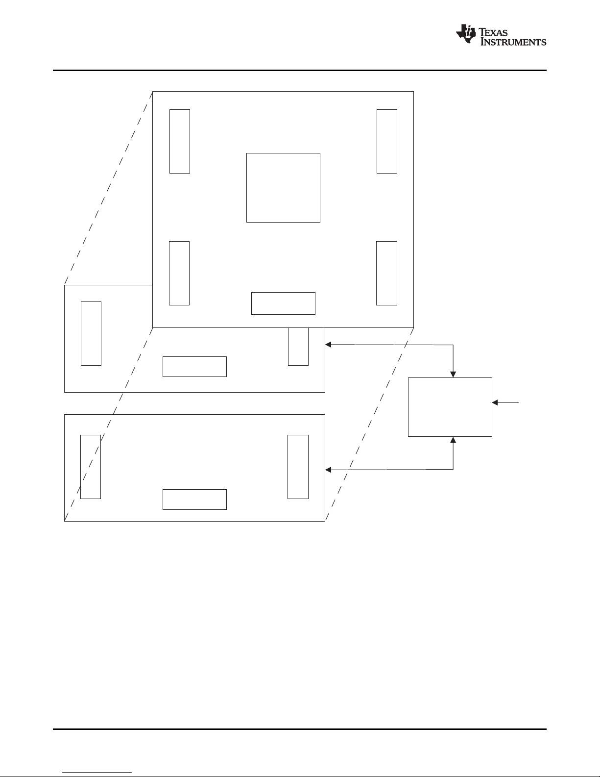
6.1 TLV320AIC12KEVMB-K/14KEVMB-K Block Diagram
A block diagram of the TLV320AIC12KEVMB-K/14KEVMB-K is shown in Figure 1 . The evaluation kit
consists of two circuit boards connected together. The motherboard is designated as the USB-MODEVM
Interface board, while the daughtercard is the TLV320AIC12KEVMB/14KEVMB described previously in
this manual.
SLAU229B – October 2007 – Revised August 2008 TLV320AIC12KEVMB-K and TLV320AIC14KEVMB-K User's Guide 7
Submit Documentation Feedback
Page 8
EVMPosition2
EVMPosition1
TLV320AIC12KEVMB/14KEVMB
ControlInterface
TAS1020B
USB8051
Microcontroller
USB
I C
2
SMARTDM
AudioInterface
TLV320AIC12K/14K
Kit Operation
www.ti.com
Figure 1. TLV320AIC12KEVMB-K/14KEVMB-K Block Diagram
The USB-MODEVM Interface board is intended to be used in USB mode, where control of the installed
EVM is accomplished using the onboard USB controller device. Provision is made, however, for driving all
the data buses (I2C, PCM/ SMARTDM™) externally. The source of these signals is controlled by SW2 on
the USB-MODEVM. Refer to Table 6 for details on the switch settings.
Additionally, SW3 on the USB-MODEVM (IOVDD SELECT) must be set up to 3.3V (SW3 position 1 on,
SW3 positions 2-8 off).
TLV320AIC12KEVMB-K and TLV320AIC14KEVMB-K User's Guide8 SLAU229B – October 2007 – Revised August 2008
Submit Documentation Feedback
Page 9

www.ti.com
Kit Operation
Table 6. USB-MODEVM SW2 Settings
SW-2 SWITCH
NUMBER LABEL SWITCH DESCRIPTION
1 A0 ON: A0 = 0
2 A1 ON: A1 = 0
3 A2 ON: A2 = 0
4 USB I2S ON: Digital Audio Bus connects to TAS1020
5 USB MCK ON: MCLK connects to TAS1020
6 USB SPI ON: SPI Bus connects to TAS1020
7 USB RST ON: EVM Reset Signal comes from TAS1020
8 EXT MCK ON: MCLK Signal is provided from USB-MODEVM J10
USB-MODEVM EEPROM I2C Address A0
OFF: A0 = 1
USB-MODEVM EEPROM I2C Address A1
OFF: A1 = 1
USB-MODEVM EEPROM I2C Address A2
OFF: A2 = 1
Digital Audio Bus Source Selection
OFF: Digital Audio Bus connects to USB-MODEVM J14
Digital Audio Bus MCLK Source Selection
OFF: MCLK connects to USB-MODEVM J14
SPI Bus Source Selection
OFF: SPI Bus connects to USB-MODEVM J15
RST Source Selection
OFF: EVM Reset Signal comes from USB-MODEVM J15
External MCLK Selection
OFF: MCLK Signal comes from either selection of SW2-5
For use with the TLV320AIC12KEVMB/14KEVMB, SW-2 positions 1, 3, 4, 5 and 6 should be set to ON,
while SW-2 positions 2, 7 and 8 should be set to OFF.
6.2 Installation
Ensure that the TLV320AIC12KEVMB/14KEVMB is installed on the USB-MODEVM Interface board,
aligning J1, J2, J3, J4, J5 with the corresponding connectors on the USB-MODEVM.
Place the CD-ROM into your PC CD-ROM drive. Locate the Setup program on the disk, and start it. The
Setup program will install the TLV320AIC12K/14K Evaluation Tool software on your PC.
The NI-VISA Runtime installer is embedded to the TLV320AIC12K/14K Evaluation Tool installer. This
software allows the program to communicate with the USB-MODEVM.
When the installation completes, click Finish on the TLV320AIC12K/14K Evaluation Tool installer window.
You may be prompted to restart your computer.
When installation is complete, attach a USB cable from your PC to the USB-MODEVM Interface board. As
configured at the factory, the board will be powered from the USB interface, so the power indicator LEDs
and the 'USB ACTIVE' LED on the USB-MODEVM should light.
The Found New Hardware Wizard will show up on the screen. Select the ' No, not this time' radio button
and click ' Next >'. Select ' Install the software automatically (Recommended)' and click ' Next >'. If the
driver installs correctly the message: ' The wizard has finished installing the software for: AIC12K/14K
EVM' should appear. Click ' Finish'. The AIC12K/14K EVM driver should now be installed. The device
should now appear on the Device Manager as ' NI-VISA USB Devices>AIC12K/14K EVM' and as ' Sound,
video and game controllers>USB Audio Device'.
Once the device drivers are installed launch the TLV320AIC12K/14K Evaluation Tool software on your
PC, located on the computer's desktop or in 'Start>Programs>Texas Instruments'.
The software should automatically find the TLV320AIC12K/14K, and a screen similar to the one in
Figure 2 should appear.
SLAU229B – October 2007 – Revised August 2008 TLV320AIC12KEVMB-K and TLV320AIC14KEVMB-K User's Guide 9
Submit Documentation Feedback
Page 10
Kit Operation
www.ti.com
6.3 USB-MODEVM Interface Board
The simple diagram shown in Figure 1 shows only the basic features of the USB-MODEVM Interface
board. The board is built around a TAS1020B streaming audio USB controller with an 8051-based core.
The board features two positions for modular EVMs, or one double-wide serial modular EVM may be
installed.
Since the TLV320AIC12KEVMB/14KEVMB is a double-wide modular EVM, it is installed with connections
to both EVM positions, which connects the TLV320AIC12K/14K digital control interface to the I2C port
realized using the TAS1020B, as well as the TAS1020B digital audio interface.
In the factory configuration, the board is ready to use with the TLV320AIC12KEVMB/14KEVMB. To view
all the functions and configuration options available on the USB-MODEVM board, see the USB-MODEVM
Interface Board schematic in Appendix B .
6.4 Program Description
After the TLV320AIC12KEVMBK/14KEVMB-K software installation (described in Section 6.2 ) is complete,
evaluation and development with the TLV320AIC12K/14K can begin.
TLV320AIC12KEVMB-K and TLV320AIC14KEVMB-K User's Guide10 SLAU229B – October 2007 – Revised August 2008
Figure 2. Default Software Screen
Submit Documentation Feedback
Page 11

www.ti.com
6.5 Indicators and Main Screen Controls
Figure 2 illustrates the indicators and the main screen controls near the top of the software screen display,
and a large tabbed interface below. This section discusses the controls above this tabbed section.
At the top left of the screen is an Interface indicator. The TLV320AIC12K/14K has an I2C interface. The
indicator is lit after the program begins. Below the Interface indicator is the Device Connected indicator.
The TLV320AIC12K/14K Evaluation Tool detects whether or not the TLV320AIC12KEVMB-K/14KEVMB-K
is present. If the device is unplugged from the USB port or if the device driver is not installed properly, the
Device Connected indicator will turn red. Otherwise, it will turn green.
To the right of the Interface indicator is a group box called Firmware. This box indicates the product
identification of the USB device, so AIC12K/14K EVM should be displayed in the box labeled Located
On:. The version of the firmware appears in the Version box below this.
To the right, the next group box contains controls for resetting the TLV320AIC12K/14K. A software reset
can be done by writing to a register in the TLV320AIC12K/14K; the writing is accomplished by pushing the
button labeled Software Reset. This button also resets to the default I2C address and refreshes the GUI's
register table and controls/indicators by reading all registers. The TLV320AIC12K/14K also may be reset
by toggling a GPIO pin on the USB-MODEVM, which is done by pushing the Hardware Reset button.
In order to perform a hardware reset, the RESET jumper (W7) must be installed
and SW2-7 on the USB-MODEVM must be turned OFF. Failure to do either of
these steps results in not generating a hardware reset or causing unstable
operation of the EVM, which may require cycling power to the USB-MODEVM.
Kit Operation
CAUTION
The ADC Overflow and DAC Overflow indicators light when the overflow flags are set in register 1 of the
TLV320AIC12K/14K. These indicators, as well as the other indicators on this panel, update only when
writing or reading registers, on resets or by pushing the Refresh button. The Indicator Updates and
Control Updates buttons enable/disable updates of indicators and controls, respectively.
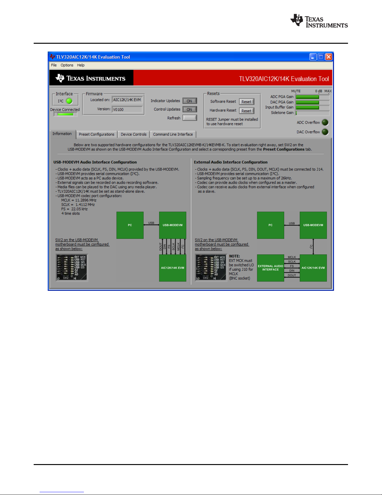
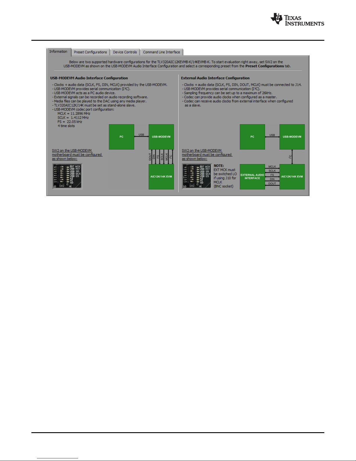
6.6 Information Tab
The information tab (Figure 3 ) shows information for two TLV320AIC12KEVMB-K/14KEVMB-K hardware
configurations.
The USB-MODEVM Audio Interface Configuration allows audio data and I2C communication between
the host computer and the TLV320AIC12K/14K. SW2 on the USB-MODEVM must be configured as
shown in the left section of Figure 3 .
SLAU229B – October 2007 – Revised August 2008 TLV320AIC12KEVMB-K and TLV320AIC14KEVMB-K User's Guide 11
Submit Documentation Feedback
Page 12
Kit Operation
www.ti.com
Figure 3. Information Tab
Additionally, the operating system's audio device must be configured as AIC12K/14K EVM (see Figure 4 ).
The External Audio Interface Configuration only allows I2C communication between the host computer
and the TLV320AIC12K/14K. In this configuration, the TLV320AIC12K/14K can transmit and receive audio
data to/from an external PCM device or DSP. SW2 on the USB-MODEVM must be configured as shown in
the right section of Figure 3 .
12 TLV320AIC12KEVMB-K and TLV320AIC14KEVMB-K User's Guide SLAU229B – October 2007 – Revised August 2008
Submit Documentation Feedback
Page 13

www.ti.com
Kit Operation
Figure 4. Sounds and Audio Devices Properties
6.7 Preset Configurations Tab
The Preset Configurations tab (Figure 5 ) provides several presets for both the USB-MODEVM Audio
Interface Configuration and the External Audio Interface Configuration. Also, there is a
TLV320AIC12K/14K Defaults preset which programs the codec's default register settings. When a radio
button is selected, a detailed description of the preset will appear on the Preset Configuration
Description box. To load a preset to the codec, select the desired preset by selecting the corresponding
radio button and pushing the Load button. At the same time, this will show the preset's executed
commands on the Command Buffer of the Command Line Interface tab (see Figure 13 ).
SLAU229B – October 2007 – Revised August 2008 TLV320AIC12KEVMB-K and TLV320AIC14KEVMB-K User's Guide 13
Submit Documentation Feedback
Page 14

Kit Operation
www.ti.com
6.8 Device Controls Tab
The Device Controls Tab (Figure 6 ) contains six enumerated Control Registers sub tabs with controls
for all six registers of the TLV320AIC12K/14K, a register table at the bottom of the tab, several controls
and an indicator at the right of the tab. The 8-bit I2C Address indicator shows the current I2C address.
The Device Position control lets the user select a specific codec on a master-slave chain to write to or
read from. The TLV320AIC12KEVMB-K/14KEVMB-K is configured as a stand-alone slave, so the device
position must be set to zero. The Program Device button, when pushed, programs the register
corresponding only to the selected Control Registers sub tab. The register table holds the current
register values in hexadecimal and binary format. The Register Dump to File button dumps the current
register values to a spreadsheet. Please refer to the TLV320AIC12K/14K datasheet for further details on
control register content.
Figure 5. Preset Configurations
14 TLV320AIC12KEVMB-K and TLV320AIC14KEVMB-K User's Guide SLAU229B – October 2007 – Revised August 2008
Submit Documentation Feedback
Page 15

www.ti.com
Kit Operation
6.8.1 Control Register 1 Tab
The Transfer Mode control lets the user select between continuous data transfer mode or programming
mode. In the continuous data transfer mode, only audio data is sent and received through the serial audio
bus. In the programming mode, control data is sent and received through the serial audio bus. The Data
Format Mode, if set to 15 bits + 1, allows the codec to run in continuous mode and switch to
programming mode by setting the LSB of DIN to 1 to send control data. The USB-MODEVM Audio
Interface Configuration currently supports continuous and 16-bits audio data transfers. The Mic Bias sets
the voltage of the BIAS pin to 2.35V or 1.35V. The Selected Filter button allows the user to select
between an FIR filter or an IIR filter for the decimation/interpolation low-pass filter. The Loopback
switches toggle the analog or digital loopback on and off. The indicator below each switch will light when
on only if the register data sent by pressing the Program Device button is acknowledged.
Figure 6. Device Controls Tab
SLAU229B – October 2007 – Revised August 2008 TLV320AIC12KEVMB-K and TLV320AIC14KEVMB-K User's Guide 15
Submit Documentation Feedback
Page 16

Kit Operation
6.8.2 Control Register 2 Tab
The Turbo Mode control (Figure 8 ) sets the SCLK frequency to 16 × FS × (number of devices) × mode or
MCLK ÷ P, where number of devices is the number of codecs in cascade (default=1) and the mode is 1 for
continuous data transfer mode and 2 for programming mode. The Host Port Control can be used to
assign different functions to the SDA pin or to set SCL and SDA for I2C or S2C. When using the
USB-MODEVM Audio Interface Configuration the Host Port Control must be set to SDA/SCL are I2C
interface pins.
If the host interface is not needed, the two pins of SCL and SDA can be programmed to become
general-purpose I/Os. If selected to be used as I/O pins, the SDA and SCL pins become output and input
pins respectively, determined by D1 and D0. SDA can then be set to 1 or 0 by toggling the General
Purpose Output control.
The Decimation/Interpolation filter bypass button bypasses the filters selected in register 1. This can be
useful when using a DSP to apply such filters. The I2C Base Address control allows the user to select the
first three bits (MSB first) of the device's 7-bit I2C address. The last 4 bits of the address will depend on
the automatic cascade detection (ACD) feature of SMARTDM™, which sets the device position.
www.ti.com
Figure 7. Control Register 1 Tab
16 TLV320AIC12KEVMB-K and TLV320AIC14KEVMB-K User's Guide SLAU229B – October 2007 – Revised August 2008
Submit Documentation Feedback
Page 17

www.ti.com
6.8.3 Control Register 3 Tab
The Control Register 3 Tab (Figure 9 ) allows the user to set the DAC Oversampling Rate (OSR), set
the Asynchronous Sampling Rate Factor and power down the ADC or DAC with the Power Down
Controls. The indicator below each power down switch will light when on only if the register data sent by
pressing the Program Device button is acknowledged. The USB-MODEVM Audio Interface
Configuration currently allows a fixed sampling rate and a single codec. For an OSR=256 the value of M,
set in register 4, must be a multiple of 2. Similarly, for an OSR=512 the value of M must be a multiple of 4.
Kit Operation
Figure 8. Control Register 2 Tab
6.8.4 Control Register 4 Tab
The Control Register 4 Tab (Figure 10 ) provides controls for P, N and M. Furthermore, an FS calculator
is provided for convenience. The calculator derives FS from the MCLK frequency entered by the user or
loaded by a preset by using the equation: FS=MCLK ÷ (16 × P × M × N). The PLL Method switch illustrates
that for coarse sampling, P must be equal to 8. Please note that the FS calculator and the PLL Method
SLAU229B – October 2007 – Revised August 2008 TLV320AIC12KEVMB-K and TLV320AIC14KEVMB-K User's Guide 17
Submit Documentation Feedback
Figure 9. Control Register 3 Tab
Page 18

Kit Operation
are merely for illustration; what is actually written to registers 4A and 4B are the values of P, M and N
only. The USB-MODEVM Audio Interface Configuration is set up for an MCLK=11.2896 MHz, so P, M
and N must satisfy the FS equation and the SCLK equation in Turbo Mode for that configuration. If using
the External Audio Interface Configuration, the divider values can be set to anything specified in the
TLV320AIC12K/14K datasheet.
6.8.5 Control Register 5 Tab
The Control Register 5 Tab (Figure 11 ) has several gain controls. The ADC PGA and DAC PGA gain
knobs range from -42dB to 20dB and each have a MUTE button. The gain knobs and the respective
MUTE buttons write to register 5A for the ADC PGA and to register 5B for the DAC PGA. Sliders are
provided for the Input Buffer Gain (0dB to 24dB) and the Digital Sidetone Gain (-21dB to -3dB w/ MUTE)
and they both share register 5C. For convenience, the corresponding register for each control is provided
to the right of the tab. An 'x' denotes the bits modified by the corresponding control.
www.ti.com
Figure 10. Control Register 4 Tab
6.8.6 Control Register 6 Tab
The Control Register 6 Tab (Figure 12 ) provides controls to select the analog input and to configure the
analog outputs. Note that OUTP2/P3 are only available on the TLV320AIC12/12K. The
TLV320AIC12KEVMB/14KEVMB provides a 1/8" audio jack (J8) to connect a microphone, an on-board
electret microphone (MK1) and another 1/8" audio jack (J11) to connect a stereo headset. There are four
options for the Analog Input Select control:
a. INP/M1 - selects input 1 as the input source (connected to screw terminal J10). To use this mode,
jumper W11 must be installed on pins 2-3.
b. MICIN self-biased to 1.35V (single-ended) - In this mode, the device internally self-biases the input to
1.35V. To use this mode, jumper W11 must be installed on pins 2-3. Jumper W12 must be installed if
using the on-board electret microphone (MK1), otherwise a microphone can be connected to J8.
18 TLV320AIC12KEVMB-K and TLV320AIC14KEVMB-K User's Guide SLAU229B – October 2007 – Revised August 2008
Figure 11. Control Register 5 Tab
Submit Documentation Feedback
Page 19

www.ti.com
Kit Operation
Please refer to Appendix A for details. Note that the ring contact in J8 is not connected.
c. MICIN with external common mode (pseudo-differential) - In this mode, the single ended input is
connected through ac-coupling to MICIN and the bias voltage used to generate the signal is also ac
coupled to INM1. To use this mode, jumper W11 must be installed on pins 1-2. Jumper W12 must be
installed if using the on-board electret microphone (MK1), otherwise a microphone can be connected to
J8. Please refer to Appendix A for details. Note that the ring contact in J8 is not connected.
d. INP/M2 - selects input 2 as the input source (connected to screw terminal J9).
The Output Configuration control (TLV320AIC12K only) sets outputs OUTP2/P3 to differential or
single-ended mode. If set to differential, OUTP2 and OUTP3 share pin OUTMV as the common inverting
output. If set to single-ended, OUTMV becomes a virtual ground for OUTP2/P3 at the common mode
voltage of 1.35V. Switch SW2 on the TLV320AIC12KEVMB/14KEVMB can be used to try multiple output
configurations on J7 and J11. Please see the Functional Description section on the TLV320AIC12K/14K
datasheet for details.
The Output Drivers Controls (TLV320AIC12K only) mutes and powers down OUTP2 and/or OUTP3.
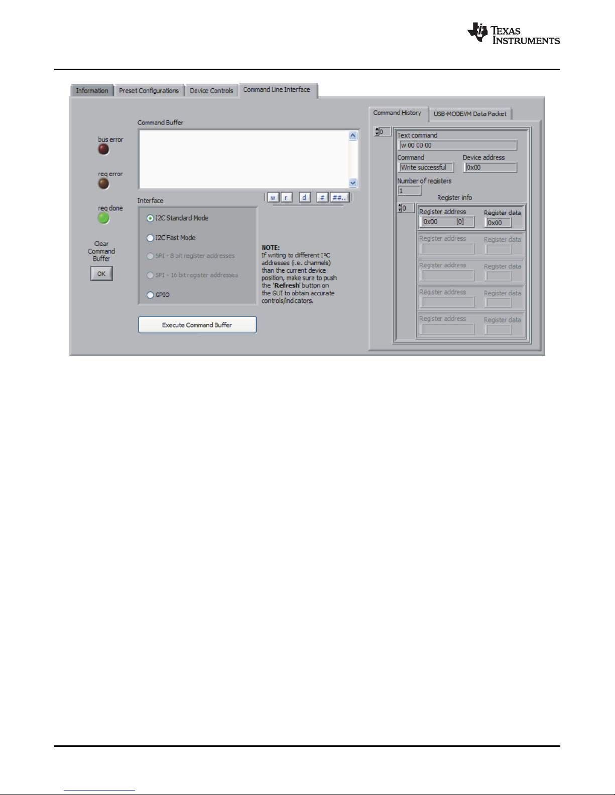
6.9 Command Line Interface Tab
A simple scripting language controls the TAS1020 on the USB-MODEVM from the LabView™-based PC
software. The main program controls, described previously, do nothing more than write a script which is
then handed off to an interpreter that sends the appropriate data to the correct USB endpoint. Because
this system is script-based, provision is made in this tab for the user to view the scripting commands that
are created as the controls are manipulated, as well as load and execute other scripts that have been
written and saved (see Figure 13 ). This design allows the software to be used as a quick test tool or to
help provide troubleshooting information in the rare event that the user encounters a problem with this
EVM.
Figure 12. Control Register 6 Tab
SLAU229B – October 2007 – Revised August 2008 TLV320AIC12KEVMB-K and TLV320AIC14KEVMB-K User's Guide 19
Submit Documentation Feedback
Page 20
Kit Operation
www.ti.com
Figure 13. Command Line Interface Tab
A script is loaded into the command buffer, either by operating the controls on the other tabs or by loading
a script file or preset.
When executed, either by loading commands from other tabs, loading a preset or pushing the Execute
Command Buffer button, an array containing executed commands will be displayed on the Command
History tab. Additionally, the return packet of data which results from the last command executed will be
displayed in the USB-MODEVM Data Packet tab. The logging function, described below, can be used to
see the results after every executed command.
The File menu (Figure 14 ) provides some options for working with scripts. The first option, Open
Command File..., loads a command file script into the command buffer. This script can then be executed
by pressing the Execute Command Buffer button.
The second option, Save Command File..., saves the contents of the command buffer into a file.
The third option is Log Script and Results..., which opens a file save dialog box. The user can choose a
location for a log file to be written using the file save dialog. When the Execute Command Buffer button is
pressed, the script will run and the script, along with resulting data read back during the script, will be
saved to the file specified. The log file is a standard text file which can be opened with any text editor, and
looks much like the source script file, but with the additional information of the result of each script
command executed.
The third menu item is a submenu of Recently Opened Files. This list is simply a list of script files that
have previously been opened, allowing fast access to commonly-used script files. The final menu item is
Exit, which terminates the TLV320AIC12K/14K Evaluation Tool software.
20 TLV320AIC12KEVMB-K and TLV320AIC14KEVMB-K User's Guide SLAU229B – October 2007 – Revised August 2008
Submit Documentation Feedback
Page 21

www.ti.com
Kit Operation
Figure 14. File Menu
The Options menu (Figure 15 ) provides two settings suitable for command line interface users and for
troubleshooting. These settings allows the user to evaluate the device in its most basic form.
The first option, Hardware Reset on Startup, enables (checked) and disables (unchecked) the hardware
reset commands every time the GUI starts. If checked, a series of commands will be sent to the TAS1020
to hardware reset the TLV320AIC12K/14K at startup. If unchecked, nothing will be written to the
TLV320AIC12K/14K when the GUI starts. This option is useful if the user wants to keep the registers
intact when closing and re-opening the GUI. Keep in mind that, every time the EVM-K is connected or
reconnected, a hardware reset must be done in order to write to the codec either by pushing the Hardware
Reset button on the GUI, pressing the push-button on the EVM or by using the command line interface.
The second option, Hardware Reset on USB reconnection, enables (checked) and disables (unchecked)
the hardware reset commands every time the EVM-K is reconnected while using the GUI. If unchecked, a
manual hardware reset must be done if writing to the codec as stated on the paragraph above.
Under the Help menu is an About... menu item (Figure 16 ) which displays information about the
TLV320AIC12KEVMB/14KEVMB software.
SLAU229B – October 2007 – Revised August 2008 TLV320AIC12KEVMB-K and TLV320AIC14KEVMB-K User's Guide 21
Submit Documentation Feedback
Figure 15. Options Menu
Page 22

Kit Operation
The actual USB protocol used as well as instructions on writing scripts are detailed in the following
subsections. While it is not necessary to understand or use either the protocol or the scripts directly,
understanding them may be helpful to some users.
6.9.1 USB-MODEVM Protocol
The USB-MODEVM is defined to be a Vendor-Specific class, and is identified on the PC system as an
NI-VISA device. Because the TAS1020 has several routines in its ROM which are designed for use with
HID-class devices, HID-like structures are used, even though the USB-MODEVM is not an HID-class
device. Data passes from the PC to the TAS1020 using the control endpoint.
Data is sent in an HIDSETREPORT (see Table 7 ):
www.ti.com
Figure 16. Help
Table 7. USB Control Endpoint
HIDSETREPORT Request
PART VALUE DESCRIPTION
bmRequestType 0x21 00100001
bRequest 0x09 SET_REPORT
wValue 0x00 don't care
wIndex 0x03 HID interface is index 3
wLength calculated by host
Data Data packet as described
below
TLV320AIC12KEVMB-K and TLV320AIC14KEVMB-K User's Guide22 SLAU229B – October 2007 – Revised August 2008
Submit Documentation Feedback
Page 23

www.ti.com
Kit Operation
The data packet consists of the following bytes, shown in Table 8 :
Table 8. Data Packet Configuration
BYTE NUMBER TYPE DESCRIPTION
Specifies serial interface and operation. The two values are logically OR'd.
Operation:
READ 0x00
WRITE 0x10
0 Interface
1 I2C Slave Address Slave address of I2C device or MSB of 16-bit reg addr for SPI
2 Length Length of data to write/read (number of bytes)
3 Register address Address of register for I2C or 8-bit SPI; LSB of 16-bit address for SPI
4..64 Data return packet is limited to 42 bytes, so advise only sending 32 bytes at any one
Interface:
GPIO 0x08
SPI_16 0x04
I2C_FAST 0x02
I2C_STD 0x01
SPI_8 0x00
Up to 60 data bytes could be written at a time. EP0 maximum length is 64. The
time.
Example usage:
Write two bytes (45, A0) to device starting at register 1 of an I2C device with address 80:
[0] 0x11
[1] 0x80
[2] 0x02
[3] 0x01
[4] 0x45
[5] 0xA0
Do the same with a fast mode I2C device:
[0] 0x12
[1] 0x80
[2] 0x02
[3] 0x01
[4] 0x45
[5] 0xA0
In each case, the TAS1020 will return, in an HID interrupt packet, the following:
[0] interface byte | status
status:
REQ_ERROR 0x80
INTF_ERROR 0x40
REQ_DONE 0x20
[1] for I2C interfaces, the I2C address as sent
for SPI interfaces, the read back data from SPI line for transmission of the corresponding byte
[2] length as sent
[3] for I2C interfaces, the reg address as sent
for SPI interfaces, the read back data from SPI line for transmission of the corresponding byte
[4..60] echo of data packet sent
SLAU229B – October 2007 – Revised August 2008 TLV320AIC12KEVMB-K and TLV320AIC14KEVMB-K User's Guide 23
Submit Documentation Feedback
Page 24

Kit Operation
www.ti.com
If the command is sent with no problem, the returning byte [0] should be the same as the sent one
logically or'd with 0x20 - in the second example above (fast mode), the returning packet should be:
[0] 0x32
[1] 0x80
[2] 0x02
[3] 0x01
[4] 0x45
[5] 0xA0
If for some reason the interface fails (for example, the I2C device does not acknowledge), it would come
back as:
[0] 0x52 --> interface | INTF_ERROR
[1] 0x80
[2] 0x02
[3] 0x01
[4] 0x45
[5] 0xA0
If the request is malformed, that is, the interface byte (byte [0]) takes on a value which is not described
above, the return packet would be:
[0] 0x93 --> 0x13 was sent, which is not valid, so 0x93 is returned
[1] 0x80
[2] 0x02
[3] 0x01
[4] 0x45
[5] 0xA0
Examples above used writes. Reading is similar:
Read two bytes from device starting at register 1 of an I2C device with address A0:
[0] 0x01
[1] 0x80
[2] 0x02
[3] 0x01
The return packet should be
[0] 0x21
[1] 0x80
[2] 0x02
[3] 0x01
[4] 0x45
[5] 0xA0
assuming that the values we wrote above starting at Register 5 were actually written to the device.
24 TLV320AIC12KEVMB-K and TLV320AIC14KEVMB-K User's Guide SLAU229B – October 2007 – Revised August 2008
Submit Documentation Feedback
Page 25

www.ti.com
6.9.1.1 GPIO Capability
The USB-MODEVM has seven GPIO lines. The user can access them by specifying the interface to be
0x08, and then using the standard format for packets—but addresses are unnecessary. The GPIO lines
are mapped into one byte (see Table 9 ):
Table 9. GPIO Pin Assignments
7 6 5 4 3 2 1 0
x P3.5 P3.4 P3.3 P1.3 P1.2 P1.1 P1.0
Example: write P3.5 to a 0, all others to 1:
[0] 0x18 --> write, GPIO
[1] 0x00 --> this value is ignored
[2] 0x01 --> length - ALWAYS a 1
[3] 0x00 --> this value is ignored
[4] 0x3F --> 00111111
The user may also read back from the GPIO to see the state of the pins. Suppose the port pins were
written as in the previous example.
Example: read the GPIO
[0] 0x08 --> read, GPIO
[1] 0x00 --> this value is ignored
[2] 0x01 --> length - ALWAYS a 1
[3] 0x00 --> this value is ignored
The return packet should be:
[0] 0x28
[1] 0x00
[2] 0x01
[3] 0x00
[4] 0x3F
Kit Operation
SLAU229B – October 2007 – Revised August 2008 TLV320AIC12KEVMB-K and TLV320AIC14KEVMB-K User's Guide 25
Submit Documentation Feedback
Page 26

Kit Operation
6.9.2 Writing Scripts
A script is simply a text file that contains data to send to the serial control buses. The scripting language is
quite simple, as is the parser for the language. Therefore, the program is not very forgiving about mistakes
made in the source script file, but the formatting of the file is simple. Consequently, mistakes should be
rare.
Each line in a script file is one command. There is no provision for extending lines beyond one line. A line
is terminated by a carriage return.
The first character of a line is the command. Commands are:
The first command, i, sets the interface to use for the commands to follow. This command must be
followed by one of the following parameters:
www.ti.com
i = = = = = = = Set interface bus to use
r = = = = = = = Read from the serial control bus
w = = = = = = = Write to the serial control bus
# = = = = = = = Comment
b = = = = = = = Break
d = = = = = = = Delay
i2cstd Standard mode I2C Bus
i2cfast Fast mode I2C bus
spi8 SPI bus with 8-bit register addressing
spi16 SPI bus with 16-bit register addressing
gpio Use the USB-MODEVM GPIO capability
For example, if a fast mode I2C bus is to be used, the script would begin with:
i i2cfast
No data follows the break command. Anything following a comment command is ignored by the parser,
provided that it is on the same line. The delay command allows the user to specify a time, in milliseconds,
that the script will pause before proceeding.
Note: UNLIKE ALL OTHER NUMBERS USED IN THE SCRIPT COMMANDS, THE DELAY TIME
IS ENTERED IN A DECIMAL FORMAT. Also, note that because of latency in the USB bus
as well as the time it takes the processor on the USB-MODEVM to handle requests, the
delay time may not be precise.
A series of byte values follows either a read or write command. Each byte value is expressed in
hexadecimal, and each byte must be separated by a space. Commands are interpreted and sent to the
TAS1020 by the program using the protocol described in Section 6.9.1 .
The first byte following a read or write command is the I2C slave address of the device (if I2C is used) or
the first data byte to write (if SPI is used—note that SPI interfaces are not standardized on protocols, so
the meaning of this byte will vary with the device being addressed on the SPI bus). The second byte is the
starting register address that data will be written to (again, with I2C; SPI varies—see Section 6.9.1 for
additional information about what variations may be necessary for a particular SPI mode). Following these
two bytes are data, if writing; if reading, the third byte value is the number of bytes to read, (expressed in
hexadecimal).
26 TLV320AIC12KEVMB-K and TLV320AIC14KEVMB-K User's Guide SLAU229B – October 2007 – Revised August 2008
Submit Documentation Feedback
Page 27

www.ti.com
Kit Operation
For example, to write the values 0x45 0xA0 to an I2C device with a slave address of 0x80, starting at a
register address of 0x01, one would write:
#example script
i i2cfast
w 80 01 45 A0
r 80 01 02
This script begins with a comment, specifies that a fast I2C bus will be used, then writes 0x45 0xA0 to the
I2C slave device at address 0x80, writing the values into registers 0x01 and 0x02. The script then reads
back two bytes from the same device starting at register address 0x01. Note that the slave device value
does not change. It is not necessary to set the R/ W bit for I2C devices in the script; the read or write
commands will do that for the user.
Any text editor may be used to write these scripts; Jedit is an editor that is highly recommended for
general usage. For more information, go to: http://www.jedit.org .
Once the script is written, it can be used in the command window by running the program, and then
selecting Open Command File... from the File menu. Locate the script and open it. The script will then be
displayed in the command buffer. The user may also edit the script once it is in the buffer and save it as
specified in Section 6.9 .
Once the script is in the command buffer, it may be executed by pressing the Execute Command Buffer
button. If the user has placed breakpoints in the script, it will execute to that point, and a dialog box will
show up with a continue button to continue executing the script.
Please refer to sections 3.1 (Power Down and Reset) and section 3.2 (AIC12 Control Register
Programming Procedures) on the TLV320AIC12/13/14/15 Codec Operating In Stand-Alone Slave Mode
application note for important details on programming the codec.
Special care must be taken when writing subregisters (4A-4B and 5A-5D).
Example: w 80 01 45 A0 01 20 B8 00
The previous command writes registers 1, 2, 3, 4A, 5C and 6. It will not increment from 3 to 4A and
then to 4B. The subregister to be written will depend on the data.
SLAU229B – October 2007 – Revised August 2008 TLV320AIC12KEVMB-K and TLV320AIC14KEVMB-K User's Guide 27
Submit Documentation Feedback
Page 28

Kit Operation
www.ti.com
Here is an example of a script:
# TLV320AIC12K/14K
# This configuration allows playing audio to the DAC from any media player on
# a computer and recording from the ADC on audio recording software. Pin
# MICIN is configured as the input. The input can be heard via OUTP1/M1 and
# OUTP2/P3 due to the digital sidetone. Audio files played on the computer
# can also be heard via those outputs.
#
# Hardware reset codec using TAS1020B's GPIO pin P3.5
i gpio
w 00 00 3F
# Delay has to be at least 6 MCLK cycles ~ 540ns
d 1
w 00 00 7F
#
# I2C interface
i i2cstd
#
# reg 03 - Software reset
w 80 03 21
#
# reg 01 - Clear ADC and DAC overflow flags.
r 80 01 01
#
# reg 02 - Turbo Mode
w 80 01 A0
#
# reg 04 - Set clock divider values (4A and 4B). P=8, M=1, N=4.
w 80 04 20
w 80 04 81
#
# reg 05 - 5B -> DAC PGA=–32dB, 5C -> Input Buffer Gain=24dB,
# Digital Sidetone Gain=–3dB. Defaults used for 5A and 5D.
w 80 05 4A
w 80 05 83
#
# reg 06 - MICIN with external common mode, OUTP2/P3 drivers on.
w 80 06 1C
#
# reg 01 - Continuous data transfer mode, 16 bits.
w 80 01 41
TLV320AIC12KEVMB-K and TLV320AIC14KEVMB-K User's Guide28 SLAU229B – October 2007 – Revised August 2008
Submit Documentation Feedback
Page 29

www.ti.com
7 EVM Bill of Materials
Table 10 and Table 11 contain a complete bill of materials for the modular
TLV320AIC12KEVMB/14KEVMB and the USB-MODEVM Interface Board.
REFERENCE DESIGNATOR DESCRIPTION MANUFACTURER MFG PART NUMBER
R7, R8 0 Ω 1/10W 5% chip resistor Panasonic (or equivalent) ERJ-3GEY0R00V
R5 2.7k Ω 1/10W 5% chip resistor Panasonic (or equivalent) ERJ-3GEYJ272V
R1-R4, R6 10k Ω 1/10W 5% chip resistor Panasonic (or equivalent) ERJ-3GEYJ103V
C8-C10, C19 0.1 µ F 6.3V ceramic chip TDK (or equivalent) C1005X5R0J104K
C1–C6, C11, C12, C20, C21 0.1 µ F 25V ceramic chip TDK (or equivalent) C1608X7R1E104K
C13-C15, C18 10 µ F 6.3V ceramic chip Panasonic (or equivalent) ECJ-1VB0J106M
C16, C17 10 µ F 16V ceramic chip TDK (or equivalent) C3216X5R0J106M
C22, C23 47 µ F 10V ceramic chip Murata (or equivalent) GRM32ER61A476KE20L
U1 Audio codec Texas Instruments TLV320AIC12KIDBT
U2 3.3V LDO voltage regulator Texas Instruments REG1117-3.3
U3 64K I2C EEPROM MicroChip 24LC64-I/SN
U4 Pos edge triggered D Flip-flop Texas Instruments SN74AUP1G74
J6, J9, J10 Screw terminal block, On Shore Technology ED555/2DS
J7 Screw terminal block, On Shore Technology ED555/3DS
J8, J11 3.5mm audio jack, T-R-S, SMD CUI Inc. SJ1-3515-SMT
J1A, J2A, J4A, J5A 20-pin SMT plug Samtec TSM-110-01-L-DV-P
J1B, J2B, J4B, J5B 20-pin SMT socket Samtec SSW-110-22-F-D-VS-K
J3A 10-pin SMT plug Samtec TSM-105-01-L-DV-P
J3B 10-pin SMT socket Samtec SSW-105-22-F-D-VS-K
N/A TLV320AIC12KEVMB/14KEVM Texas Instruments 6488702
W3, W4, W6-W10, W12 2-position jumper, 0.1" spacing Samtec TSW-102-07-L-S
W1, W2, W5, W11 3-position jumper, 0.1" spacing Samtec TSW-103-07-L-S
MK1 Omnidirectional microphone Knowles Acoustics MD9745APZ-F
SW1 Switch LT TOUCH 6X3.5 Panasonic - ECG EVQ-PJU04K
SW2 4PDT right angle switch E-Switch EG4208
TP13–TP16, TP27 PC Test Point - Miniature (red) Keystone Electronics 5000
TP11, TP12 PC Test Point - Miniature Keystone Electronics 5001
TP1-TP10, TP17-TP26 PC Test Point - Miniature Keystone Electronics 5002
N/A Header shorting block Samtec SNT-100-BK-T
EVM Bill of Materials
Table 10. TLV320AIC12KEVMB/14KEVMB Bill of Materials
capacitor, ± 10%, X5R
capacitor, ± 5%, X7R
capacitor, ± 10%, X5R
capacitor, ± 20%, X5R
capacitor, ± 10%, X5R
TLV320AIC14KIDBT
2-position
3-position
B PWB
cartridge
240GF SMD
(black)
(white)
SLAU229B – October 2007 – Revised August 2008 TLV320AIC12KEVMB-K and TLV320AIC14KEVMB-K User's Guide 29
Submit Documentation Feedback
Page 30

EVM Bill of Materials
www.ti.com
Table 11. USB-MODEVM Bill of Materials
Designators Description Manufacturer Mfg. Part Number
R4 10 Ω 1/10W 5% chip resistor Panasonic ERJ-3GEYJ100V
R10, R11 27.4 Ω 1/16W 1% chip resistor Panasonic ERJ-3EKF27R4V
R20 75 Ω 1/4W 1% chip resistor Panasonic ERJ-14NF75R0U
R19 220 Ω 1/10W 5% chip resistor Panasonic ERJ-3GEYJ221V
R14, R21, R22 390 Ω 1/10W 5% chip resistor Panasonic ERJ-3GEYJ391V
R13 649 Ω 1/16W 1% chip resistor Panasonic ERJ-3EKF6490V
R9 1.5k Ω 1/10W 5% Panasonic ERJ-3GEYJ152V
chip resistor
R1, R2, R3, R5, R6, R7, R8 2.7k Ω 1/10W 5% Panasonic ERJ-3GEYJ272V
chip resistor
R12 3.09k Ω 1/16W 1% Panasonic ERJ-3EKF3091V
chip resistor
R15, R16 10k Ω 1/10W 5% Panasonic ERJ-3GEYJ103V
chip resistor
R17, R18 100k Ω 1/10W 5% Panasonic ERJ-3GEYJ104V
chip resistor
RA1 10k Ω 1/8W Octal isolated CTS Corporation 742C163103JTR
resistor array
C18, C19 33pF 50V ceramic TDK C1608C0G1H330J
chip capacitor, ± 5%, NPO
C13, C14 47pF 50V ceramic TDK C1608C0G1H470J
chip capacitor, ± 5%, NPO
C20 100pF 50V ceramic TDK C1608C0G1H101J
chip capacitor, ± 5%, NPO
C21 1000pF 50V ceramic TDK C1608C0G1H102J
chip capacitor, ± 5%, NPO
C15 0.1 µ F 16V ceramic TDK C1608X7R1C104K
chip capacitor, ± 10%,X7R
C16, C17 0.33 µ F 16V ceramic TDK C1608X5R1C334K
chip capacitor, ± 20%,Y5V
C9, C10, C11, C12, C22, C23, 1 µ F 6.3V ceramic TDK C1608X5R0J105K
C24, C25, C26, C27, C28 chip capacitor, ± 10%, X5R
C1, C2, C3, C4, C5, C6, C7, 10 µ F 6.3V ceramic TDK C3216X5R0J106K
C8 chip capacitor, ± 10%, X5R
D1 50V, 1A, Diode MELF SMD Micro Commercial Components DL4001
D2 Yellow Light Emitting Diode Lumex SML-LX0603YW-TR
D3, D4, D6, D7 Green Light Emitting Diode Lumex SML-LX0603GW-TR
D5 Red Light Emitting Diode Lumex SML-LX0603IW-TR
Q1, Q2 N-Channel MOSFET Zetex ZXMN6A07F
X1 6MHz Crystal SMD Epson MA-505 6.000M-C0
U8 USB streaming controller Texas Instruments TAS1020BPFB
U2 5V LDO regulator Texas Instruments REG1117-5
U9 3.3V/1.8V dual output Texas Instruments TPS767D318PWP
LDO regulator
U3, U4 Quad, 3-state buffers Texas Instruments SN74LVC125APW
U5, U6, U7 Single IC buffer driver with Texas Instruments SN74LVC1G07DBVR
open drain o/p
U10 Single 3-state buffer Texas Instruments SN74LVC1G125DBVR
U1 64K 2-Wire serial EEPROM Microchip 24LC64I/SN
I2C
USB-MODEVM PCB Texas Instruments 6463995
30 TLV320AIC12KEVMB-K and TLV320AIC14KEVMB-K User's Guide SLAU229B – October 2007 – Revised August 2008
Submit Documentation Feedback
Page 31

www.ti.com
EVM Bill of Materials
Table 11. USB-MODEVM Bill of Materials (continued)
Designators Description Manufacturer Mfg. Part Number
TP1, TP2, TP3, TP4, TP5, Miniature test point terminal Keystone Electronics 5000
TP6, TP9, TP10, TP11
TP7, TP8 Multipurpose test point Keystone Electronics 5011
J7 USB type B slave connector Mill-Max 897-30-004-90-000000
J1, J2, J3, J4, J5, J8 2-position terminal block On Shore Technology ED555/2DS
J9 2.5mm power connector CUI Stack PJ-102B
J10 BNC connector, female, AMP/Tyco 414305-1
J11A, J12A, J21A, J22A 20-pin SMT plug Samtec TSM-110-01-L-DV-P
J11B, J12B, J21B, J22B 20-pin SMT socket Samtec SSW-110-22-F-D-VS-K
J13A, J23A 10-pin SMT plug Samtec TSM-105-01-L-DV-P
J13B, J23B 10-pin SMT socket Samtec SSW-105-22-F-D-VS-K
J6 4-pin double row header (2x2) Samtec TSW-102-07-L-D
J14, J15 12-pin double row header (2x6) Samtec TSW-106-07-L-D
JMP1–JMP4 2-position jumper, Samtec TSW-102-07-L-S
JMP8–JMP14 2-position jumper, Samtec TSW-102-07-L-S
JMP5, JMP6 3-position jumper, Samtec TSW-103-07-L-S
JMP7 3-position dual row jumper, Samtec TSW-103-07-L-D
SW1 SMT, half-pitch C & K Division, ITT TDA02H0SK1
SW2 SMT, half-pitch C & K Division, ITT TDA08H0SK1
terminal
thru-hole
PC mount
0.1"
0.1"
0.1" spacing
0.1" spacing
0.1" spacing
0.1" spacing
2-position switch
8-position switch
Jumper plug Samtec SNT-100-BK-T
SLAU229B – October 2007 – Revised August 2008 TLV320AIC12KEVMB-K and TLV320AIC14KEVMB-K User's Guide 31
Submit Documentation Feedback
Page 32

Appendix A
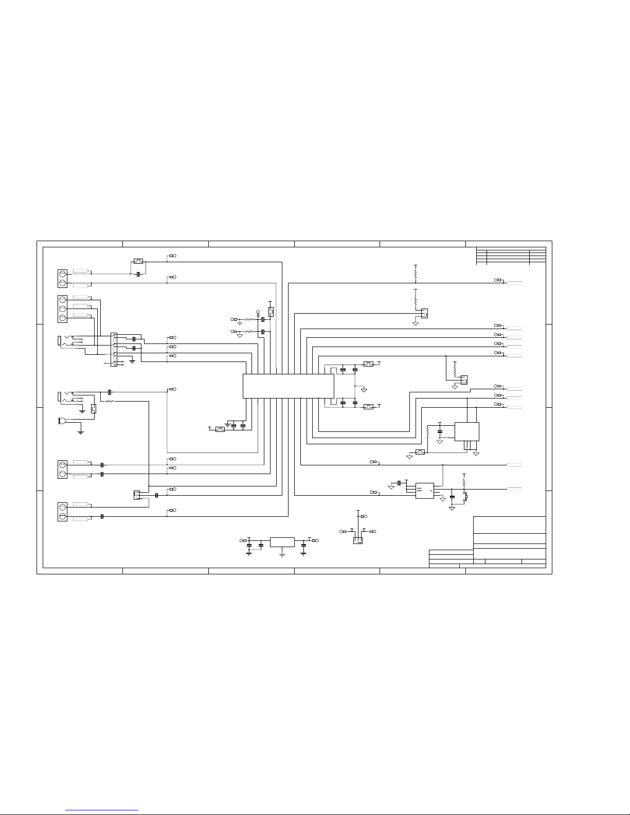
Appendix A TLV320AIC12KEVMB/14KEVMB Schematic
The schematic diagram is provided as a reference.
www.ti.com
32 TLV320AIC12KEVMB/14KEVMB Schematic SLAU229B – October 2007 – Revised August 2008
Submit Documentation Feedback
Page 33

1 2 3 4 5 6
A
B
C
D
6
54321
D
C
B
A
ti
12500 TI Boulevard, Dallas, TX 75243 USA
TITLE
SHEET OF FILE
SIZE
DATE REV19-Aug-2008
DRAWN BY
ENGINEER
REVISION HISTORY
REV ENGINEERING CHANGE NUMBER APPROVED
B
DATA ACQUISITION PRODUCTS
HIGH-PERFORMANCE ANALOG DIVISION
SEMICONDUCTOR GROUP
Jorge Arbona
Steve Leggio
Daughtercard_Interface.Sch
B
23
TLV320AIC12K_14K_DBT_EVMB
DOCUMENT CONTROL NO.N/A
GPIO0
2
DGND
4
GPIO1
6
GPIO2
8
DGND
10
GPIO3
12
GPIO4
14
SCL
16
DGND
18
SDA
20
CNTL
1
CLKX
3
CLKR
5
FSX
7
FSR
9
DX
11
DR
13
INT
15
TOUT
17
GPIO5
19
J5A
DAUGHTER-SERIAL
A0(+)
2
A1(+)
4
A2(+)
6
A3(+)
8
A4
10
A5
12
A6
14
A7
16
REF-
18
REF+
20
A0(-)
1
A1(-)
3
A2(-)
5
A3(-)
7
AGND
9
AGND
11
AGND
13
VCOM
15
AGND
17
AGND
19
J1A
DAUGHTER-ANALOG
-VA
2
-5VA
4
AGND
6
VD1
8
+5VD
10
+VA
1
+5VA
3
DGND
5
+1.8VD
7
+3.3VD
9
J3A
DAUGHTER-POWER
GPIO0
2
DGND
4
GPIO1
6
GPIO2
8
DGND
10
GPIO3
12
GPIO4
14
SCL
16
DGND
18
SDA
20
CNTL
1
CLKX
3
CLKR
5
FSX
7
FSR
9
DX
11
DR
13
INT
15
TOUT
17
GPIO5
19
J4A
DAUGHTER-SERIAL
MCLK
DIN
DOUT
FSD
SCLK
PWDN
RESET
SDA
SCL
J1A (TOP) = SAMTEC - P/N: TSM-110-01-L-DV-P
J1B (BOTTOM) = SAMTEC - P/N: SSW-110-22-F-D-V
J5A (TOP) = SAMTEC - P/N: TSM-110-01-L-DV-P
J5B (BOTTOM) = SAMTEC - P/N: SSW-110-22-F-D-V
J4A (TOP) = SAMTEC - P/N: TSM-110-01-L-DV-P
J4B (BOTTOM) = SAMTEC - P/N: SSW-110-22-F-D-V
J3A (TOP) = SAMTEC - P/N: TSM-105-01-L-DV-P
J3B (BOTTOM) = SAMTEC - P/N: SSW-105-22-F-D-V
+5VA
A0(+)
2
A1(+)
4
A2(+)
6
A3(+)
8
A4
10
A5
12
A6
14
A7
16
REF-
18
REF+
20
A0(-)
1
A1(-)
3
A2(-)
5
A3(-)
7
AGND
9
AGND
11
AGND
13
VCOM
15
AGND
17
AGND
19
J2A
DAUGHTER-ANALOG
J2A (TOP) = SAMTEC - P/N: TSM-110-01-L-DV-P
J2B (BOTTOM) = SAMTEC - P/N: SSW-110-22-F-D-VS-K
AGNDDGND
+3.3VD
+1.8VD
OUTMV
OUTP2
OUTP3
INM2 INP2
INP1INM1
OUTP1OUTM1
DIN
DOUT
MCLK
SCL
SDA
GPIO0
2
DGND
4
GPIO1
6
GPIO2
8
DGND
10
GPIO3
12
GPIO4
14
SCL
16
DGND
18
SDA
20
CNTL
1
CLKX
3
CLKR
5
FSX
7
FSR
9
DX
11
DR
13
INT
15
TOUT
17
GPIO5
19
J5B
DAUGHTER-SERIAL
FS
OUTMV
1 2
W7
/J1B
/J2B
/J4B
/J3B
Page 34
1 2 3 4 5 6
A
B
C
D
6
54321
D
C
B
A
ti
12500 TI Boulevard, Dallas, TX 75243 USA
TITLE
SHEET OF FILE
SIZE
DATE REV19-Aug-2008
DRAWN BY
ENGINEER
REVISION HISTORY
REV ENGINEERING CHANGE NUMBER APPROVED
B
DATA ACQUISITION PRODUCTS
HIGH-PERFORMANCE ANALOG DIVISION
SEMICONDUCTOR GROUP
Jorge Arbona
Steve Leggio
AIC12K_14K_DBT.Sch
B
33
TLV320AIC12K_14K_DBT_EVMB
DOCUMENT CONTROL NO.N/A
MCLK
DIN
DOUT
FS
SCLK
RESET
PWDN
SDA
SCL
R2
10K
IOVDD
VCC
8
VSS
4
SDA5SCL
6
A01A12A23WP
7
U3
24LC64I/SN
C12
0.1uF
R5
2.7K
1 2
W6
INP1
INM1
TP25
MCLK
TP26
/RESET
TP20
FS
TP22
SCLK
TP19
DOUT
TP18
DIN
TP23
SDA
TP24
SCL
TP17
PWDN
+3.3VD
MICBIAS
MICIN
OUTP1
EXT MIC IN
INM1
1
2
J6
OUT1
VIN3VOUT
2
GND
1
U2
REG1117-3.3
INM2
OUTM1
1
2
3
J7
OUT2
INP2
+5VA
C16
10uF
C4
0.1uF
C11
0.1uF
TP9
INM1
C17
10uF
TP10
INP1
1
2
J10
IN1
INP1
+3.3VA
TP11
AGND
C3
0.1uF
TP12
DGND
C2
0.1uF
TP8
INM2
TP13
+5VA
TP7
INP2
1
2
J9
IN2
TP14
+3.3VA
+3.3VD+1.8VD
C6
0.1uF
C1
0.1uF
TP15
+1.8VD
R1
10K
TP16
+3.3VD
1
2
3
W11
JMP
OUTP2
OUTMV
OUTP3
C5
0.1uF
SDA
DIN
FS
MCLK
/RESET
DOUT
FSD
+1.8V_D
M/S
IOVDD1
DGND
SCL
PWDN
SCLK
+3.3V_A
AGND
DRVDD
MICIN
MICBIAS
INP1
INM1
INP2
INM2
OUTP1
OUTM1
DRVSS
OUTP2
OUTMV
OUTP3
C13
10uFC80.1uF
+3.3VA
C15
10uF
C10
0.1uF
+1.8VD
C14
10uFC90.1uF
IOVDD
R4
10K
IOVDD
1
2
3
W2
JMP
R3
10K
IOVDD
1
2
3
W1
JMP
+3.3VA
INP2
INM2
OUTP1
OUTM1
TP2
OUTM1
TP1
OUTP1
OUTMV
OUTP3
TP5
OUTP3
TP4
OUTMV
OUTP2
TP3
OUTP2
M/S
MCLK
RESET
PWDN
DIN
DOUT
FS
1 2
W8
1 2
W3
1 2
W4
12
W9
TP6
MICIN
C18
10uF
C19
0.1uF
R6
10K
+3.3VD
CLK
1
D2PRE
7
VCC
8
GND
4
Q3CLR
6
Q
5
U4
SN74AUP1G74
C21
0.1uF
R7
0
TP27
IOVDD
IOVDD
123
W5
IOVDD
C20
0.1uF
+3.3VD
SW1
RESET
FSD
TP21
FSD
FSD
1 2
W10
TP28
DRVSS
R8
0
C23
47uF
C22
47uF
MK1
MD9745APZ-F
MICROPHONE
1 2
W12
HEADSET OUTPUT
5
4
2
3
6
1
8
7
9
11
10
12
SW2
4PDT_ESW_EG4208
5
1
3
4
2
J11
SJ1-3515-SMT
5
1
3
4
2
J8
SJ1-3515-SMT
IOVSS
1
SCLK
28
IOVDD
2
AVDD17AVSS
16
DVDD29DVSS
30
SDA27SCL26MCLK
25
FS
4
FSD
3
DIN
6
DOUT
5
M/S
7
/PWRDN
8
/RESET24INM122INP123INM220INP219BIAS
21
MICIN
18
DRVDD
11
DRVSS
12
OUTP110OUTP2
13
OUTM1
9
OUTP3
15
OUTMV
14
U1
TLV320AIC12K_DBT
Page 35

www.ti.com
Appendix B USB-MODEVM Schematic
The schematic diagram is provided as a reference.
Appendix B
SLAU229B – October 2007 – Revised August 2008 USB-MODEVM Schematic 33
Submit Documentation Feedback
Page 36

1 2 3 4 5 6
A
B
C
D
6
54321
D
C
B
A
ti
6730 SOUTH TUCSON BLVD., TUCSON, AZ 85706 USA
TITLE
SHEET OF FILE
SIZE
DATE REVdd MMM yyyy
DRAWN BY
ENGINEER
REVISION HISTORY
REV ENGINEERING CHANGE NUMBER APPROVED
B
DATA ACQUISITION PRODUCTS
HIGH-PERFORMANCE ANALOG DIVISION
SEMICONDUCTOR GROUP
FRYE D. ZERKETTS
I. C. SPOTTS
???
A
11
untitled
DOCUMENT CONTROL NO.1234567
MCLK
BCLK
LRCLK
I2SDIN
I2SDOUT
MISO
MOSI
SS
SCLK
RESET
INT
PWR_DWN
P3.3
P3.4
P3.5
P1.0
SDA
SCL
P1.1
P1.2
P1.3
Daughtercard Interface
Daughtercard Interface
MCLK
BCLK
LRCLK
I2SDIN
I2SDOUT
INT
MISO
MOSI
SS
SCLK
RESET
PWR_DWN
SDA
SCL
P3.3
P3.4
P3.5
P1.0
P1.1
P1.2
P1.3
USB Interface
USB Interface
Page 37

1 2 3 4 5 6
A
B
C
D
6
54321
D
C
B
A
ti
6730 SOUTH TUCSON BLVD., TUCSON, AZ 85706 USA
TITLE
SHEET OF FILE
SIZE
DATE REV3-Apr-2007
DRAWN BY
ENGINEER
REVISION HISTORY
REV ENGINEERING CHANGE NUMBER APPROVED
B
DATA ACQUISITION PRODUCTS
HIGH PERFORMANCE ANALOG DIVISION
SEMICONDUCTOR GROUP
RICK DOWNS
ROBERT BENJAMIN
C:\01_TI\designs\USB_MODEVM\usb-modevm_revD\USB Moth erboard - M odE vm .ddb - Docum ents\S CH \USB I nterface
D
12
USB-MODEVM INTERFACE
J9
CUI-STACK PJ102-BH
YELLOW
2.5 MM
6VDC-10VDC IN
C15
0.1uF
DOCUMENT CONTROL NO.
CSCHNE
32
CRESET
34
CSYNC
35
CDATI
36
CSCLK
37
MCLKO139MCLKO2
40
RESET
41
VREN
42
SDA43SCL
44
XTALO
46
XTALI
47
PLLFILI
48
PLLFILO
1
MCLKI
3
PUR
5
DP
6
DM
7
MRESET
9
DVSS
4
DVSS
16
DVSS
28
AVSS
45
TEST10EXTEN
11
CDATO
38
RSTO12NC20NC
22
P3.013P3.114P3.2/XINT15P3.317P3.418P3.5
19
AVDD
2
DVDD
33
DVDD
21
DVDD
8
P1.0
23
P1.1
24
P1.2
25
P1.3
26
P1.4
27
P1.5
29
P1.6
30
P1.7
31
U8
TAS1020BPFB
VCC
1
D-
2
D+
3
GND
4
J7
897-30-004-90-000000
R9
1.5K
R10
27.4
R11
27.4
C13
47pF
C14
47pF
123
JMP6
PWR SELECT
C20
100pF
C21
.001uF
R12
3.09K
X1
MA-505 6.000M-C0
C18
33pF
C19
33pF
+3.3VD
VCC
8
VSS
4
SDA5SCL
6
A01A12A23WP
7
U1
24LC64I/SN
+3.3VD
C9
0.1uF
TP9
TP10
R3
2.7KR52.7K
+3.3VD
MCLK
BCLK
LRCLK
I2SDIN
I2SDOUT
INT
MISO
MOSI
SS
SCLK
R13
649
+3.3VD
R4
10
C10
0.1uF
C11
0.1uF
C12
0.1uF
USB SLAVE CONN
EXT PWR IN
6.00 MHZ
6463996
RED
IOVDD
IOVDD
C23
0.1uF
C22
0.1uF
IOVDD
C27
0.1uF
+3.3VD
C26
0.1uF
+3.3VD
IOVDD
+3.3VD
IOVDD
TP11
MRESET
3.3VD ENABLE
1.8VD ENABLE
C17
0.33uF
C7
10uF
1GND
3
1EN
4
1IN
5
1IN
6
2GND
9
2EN
10
2IN
11
2IN
12
2OUT
17
2OUT
18
2RESET
22
1OUT
23
1OUT
24
1RESET
28
U9
TPS767D318PWP
R17
100K
+3.3VD
C8
10uF
D5
SML-LX0603IW-TR
D2
SML-LX0603YW-TR
D4
SML-LX0603GW-TR
R19
220
GREEN
USB I2S
USB MCK
USB SPI
USB SPI
USB I2S
USB MCK
+1.8VD
RESET
C24
0.1uF
USB ACTIVE
USB RST
USB RST
2
4
6
1
3
5
7 8
9 10
11 12
J15
EXTERNAL SPI
2
4
6
1
3
5
7 8
9 10
11 12
J14
EXTERNAL AUDIO DATA
PWR_DWN
J10
EXT MCLK
R20
75
+3.3VD
1
2
3
4
5
6
7
8
16
15
14
13
12
11
10
9
SW2
SW DIP-8
EXT MCK
241
3
J6
EXTERNAL I2C
IOVDD
SDA
SCL
+5VD
R15
10K
R16
10K
14
23
SW1
REGULATOR ENABLE
VIN3VOUT
2
GND
1
U2
REG1117-5
D1
DL4001
C16
0.33uF
C6
10uF
P3.3
P3.4
P3.5
P1.0
P1.1
P1.2
P1.3
J8
ED555/2DS
TP6
D3
SML-LX0603GW-TR
R14
390
GREEN
A0
A1
A2
24
1
53
U10
SN74LVC1G125DBV
C28
0.1uF
RA1
10K
VREF12VREF2
7
EN
8
GND
1
SCL2
6
SDA2
5
SCL1
3
SDA1
4
U11
PCA9306DCT
C30
0.1uF
R23
200k
C31
0.1uF
+3.3VD
IN
1
GND
2
EN
3
OUT
5
FB
4
U14
TPS73201DBV
116
215
314
413
512
611
710
89
SW3
IOVDD SELECT
C25
10uF
1.2V
1.4V
1.6V
1.8V
2.0V
2.5V
3.0V
3.3V
R27
25.5k
R29
28k
R35
46.4k
R36
30.9k
R34
36.5k
R32
48.7k
R31
32.4k
R33
39.2k
R25
22.1k
R26
137k
R28
76.8k
R30
56.2k
R18
30.1k
R37
52.3k
C37
0.1uF
VCCA
1
DIR1
2
1A1
4
1A2
5
2A1
6
2A2
7
DIR2
3
GND8GND
9
OE2
14
2B2
10
2B1
11
1B2
12
1B1
13
OE1
15
VCCB
16
U3
SN74AVC4T245PW
+3.3VD
C34
0.1uF
VCCA
1
A
3
GND
2
VCCB
6
B
4
DIR
5
U7
SN74AVC1T45DBV
C42
0.1uF
VCCA
1
A
3
GND
2
VCCB
6
B
4
DIR
5
U5
SN74AVC1T45DBV
C35
0.1uF
IOVDD
IOVDD
VCCA
1
DIR1
2
1A1
4
1A2
5
2A1
6
2A2
7
DIR2
3
GND8GND
9
OE2
14
2B2
10
2B1
11
1B2
12
1B1
13
OE1
15
VCCB
16
U12
SN74AVC4T245PW
+3.3VDIOVDD
C32
0.1uF
C33
0.1uF
EXT MCK
VCCA
1
DIR1
2
1A1
4
1A2
5
2A1
6
2A2
7
DIR2
3
GND8GND
9
OE2
14
2B2
10
2B1
11
1B2
12
1B1
13
OE1
15
VCCB
16
U4
SN74AVC4T245PW
C43
0.1uF
+3.3VD
24
1
53
U17
SN74AUP1G125DBV
C40
0.1uF
IOVDD
123
JMP7
JPR-1X3
1 2
JMP8
JPR-2X1
2 4
1
53
U15
SN74LVC1G126DBV
+3.3VD
C41
0.1uF
VCCA
1
A
3
GND
2
VCCB
6
B
4
DIR
5
U13
SN74AVC1T45DBV
C36
0.1uF
C38
0.1uF
+3.3VDIOVDD
IOVDD
+3.3VD
+3.3VD
C39
0.1uF
D8
SML-LX0603GW-TR
R24
220
GREEN
IOVDD
P3.1-P3.2
C44
1uF
+3.3VD
2 4
53
U16
SN74LVC1G06DBV
R38
10M
IOVDD
Page 38

1 2 3 4 5 6
A
B
C
D
6
54321
D
C
B
A
ti
6730 SOUTH TUCSON BLVD., TUCSON, AZ 85706 USA
TITLE
SHEET OF FILE
SIZE
DATE REV3-Apr-2007
DRAWN BY
ENGINEER
REVISION HISTORY
REV ENGINEERING CHANGE NUMBER APPROVED
B
DATA ACQUISITION PRODUCTS
HIGH-PERFORMANCE ANALOG DIVISION
SEMICONDUCTOR GROUP
RICK DOWNS
ROBERT BENJAMIN
C:\01_TI\designs\USB_MODEVM\usb-modevm_revD\USB Mother board - M odEvm .ddb - D ocum ents\SC H\D aughtercard I nterf ace
D
22
USB-MODEVM INTERFACE
DOCUMENT CONTROL NO.6463996
GPIO0
2
DGND
4
GPIO1
6
GPIO2
8
DGND
10
GPIO3
12
GPIO4
14
SCL
16
DGND
18
SDA
20
CNTL
1
CLKX
3
CLKR
5
FSX
7
FSR
9
DX
11
DR
13
INT
15
TOUT
17
GPIO5
19
J12
DAUGHTER-SERIAL
+5VD
+5VA
1 2
JMP2
1 2
JMP1
JPR-2X1
+5VA +5VD
J2
+5VA
J3
+5VD
+5VA +5VD
C2
10uF
C3
10uF
J4
+1.8VD
J5
+3.3VD
C4
10uF
C5
10uF
J1
-5VA
C1
10uF
A0(+)
2
A1(+)
4
A2(+)
6
A3(+)
8
A4
10
A5
12
A6
14
A7
16
REF-
18
REF+
20
A0(-)
1
A1(-)
3
A2(-)
5
A3(-)
7
AGND
9
AGND
11
AGND
13
VCOM
15
AGND
17
AGND
19
J11
DAUGHTER-ANALOG
GPIO0
2
DGND
4
GPIO1
6
GPIO2
8
DGND
10
GPIO3
12
GPIO4
14
SCL
16
DGND
18
SDA
20
CNTL
1
CLKX
3
CLKR
5
FSX
7
FSR
9
DX
11
DR
13
INT
15
TOUT
17
GPIO5
19
J17
DAUGHTER-SERIAL
+5VD
+5VA
A0(+)
2
A1(+)
4
A2(+)
6
A3(+)
8
A4
10
A5
12
A6
14
A7
16
REF-
18
REF+
20
A0(-)
1
A1(-)
3
A2(-)
5
A3(-)
7
AGND
9
AGND
11
AGND
13
VCOM
15
AGND
17
AGND
19
J16
DAUGHTER-ANALOG
+1.8VD
+3.3VD
+1.8VD
+3.3VD
123
JMP5
1 2
JMP3
1 2
JMP4
R2
2.7K
R1
2.7K
IOVDD
-5VA
-5VA
-5VA
MCLK
BCLK
LRCLK
I2SDIN
I2SDOUT
MISO
MOSI
SS
SCLK
RESET
P3.1-P3.2
PWR_DWN
P3.3
P3.4
P3.5
P1.0
SDA
SCL
P1.1
P1.2
P1.3
TP1 TP2 TP3
TP5
TP4
TP7
AGND
TP8
DGND
R21
390
R22
390
D7
SML-LX0603GW-TR
GREEN
D6
SML-LX0603GW-TR
GREEN
J11A (TOP) = SAM_TSM-110-01-L-DV-P
J11B (BOTTOM) = SAM_SSW-110-22-F-D-VS-
J12A (TOP) = SAM_TSM-110-01-L-DV-P
J12B (BOTTOM) = SAM_SSW-110-22-F-D-VS-
J13A (TOP) = SAM_TSM-105-01-L-DV-P
J13B (BOTTOM) = SAM_SSW-105-22-F-D-VS-
J16A (TOP) = SAM_TSM-110-01-L-DV-P
J16B (BOTTOM) = SAM_SSW-110-22-F-D-VS-
J17A (TOP) = SAM_TSM-110-01-L-DV-P
J17B (BOTTOM) = SAM_SSW-110-22-F-D-VS-
J18A (TOP) = SAM_TSM-105-01-L-DV-P
J18B (BOTTOM) = SAM_SSW-105-22-F-D-VS-
-VA
2
-5VA
4
AGND
6
VD1
8
+5VD
10
+VA
1
+5VA
3
DGND
5
+1.8VD
7
+3.3VD
9
J13
DAUGHTER-POWER
-VA
2
-5VA
4
AGND
6
VD1
8
+5VD
10
+VA
1
+5VA
3
DGND
5
+1.8VD
7
+3.3VD
9
J18
DAUGHTER-POWER
GND
1
A1
2
A2
3
A3
4
A4
5
A5
6
A6
7
A7
8
A8
9
A9
10
A10
11
A1112B11
13
B10
14
B9
15
B8
16
B7
17
B6
18
B5
19
B4
20
B3
21
B2
22
B1
23
GATE
24
U6
SN74TVC3010PW
IOVDD
+3.3VD
R6
200k
C29
0.1uF
IOVDD
R7
200k
R8
200k
+3.3VD
RA2
10k
IOVDD
INT
IOVDD
IOVDD
Page 39

FCC Warnings
This equipment is intended for use in a laboratory test environment only. It generates, uses, and can radiate radio frequency energy and
has not been tested for compliance with the limits of computing devices pursuant to subpart J of part 15 of FCC rules, which are designed
to provide reasonable protection against radio frequency interference. Operation of this equipment in other environments may cause
interference with radio communications, in which case the user at his own expense will be required to take whatever measures may be
required to correct this interference.
EVALUATION BOARD/KIT IMPORTANT NOTICE
Texas Instruments (TI) provides the enclosed product(s) under the following conditions:
This evaluation board/kit is intended for use for ENGINEERING DEVELOPMENT, DEMONSTRATION, OR EVALUATION PURPOSES
ONLY and is not considered by TI to be a finished end-product fit for general consumer use. Persons handling the product(s) must have
electronics training and observe good engineering practice standards. As such, the goods being provided are not intended to be complete
in terms of required design-, marketing-, and/or manufacturing-related protective considerations, including product safety and environmental
measures typically found in end products that incorporate such semiconductor components or circuit boards. This evaluation board/kit does
not fall within the scope of the European Union directives regarding electromagnetic compatibility, restricted substances (RoHS), recycling
(WEEE), FCC, CE or UL, and therefore may not meet the technical requirements of these directives or other related directives.
Should this evaluation board/kit not meet the specifications indicated in the User’s Guide, the board/kit may be returned within 30 days from
the date of delivery for a full refund. THE FOREGOING WARRANTY IS THE EXCLUSIVE WARRANTY MADE BY SELLER TO BUYER
AND IS IN LIEU OF ALL OTHER WARRANTIES, EXPRESSED, IMPLIED, OR STATUTORY, INCLUDING ANY WARRANTY OF
MERCHANTABILITY OR FITNESS FOR ANY PARTICULAR PURPOSE.
The user assumes all responsibility and liability for proper and safe handling of the goods. Further, the user indemnifies TI from all claims
arising from the handling or use of the goods. Due to the open construction of the product, it is the user’s responsibility to take any and all
appropriate precautions with regard to electrostatic discharge.
EXCEPT TO THE EXTENT OF THE INDEMNITY SET FORTH ABOVE, NEITHER PARTY SHALL BE LIABLE TO THE OTHER FOR ANY
INDIRECT, SPECIAL, INCIDENTAL, OR CONSEQUENTIAL DAMAGES.
TI currently deals with a variety of customers for products, and therefore our arrangement with the user is not exclusive.
TI assumes no liability for applications assistance, customer product design, software performance, or infringement of patents or
services described herein.
Please read the User’s Guide and, specifically, the Warnings and Restrictions notice in the User’s Guide prior to handling the product. This
notice contains important safety information about temperatures and voltages. For additional information on TI’s environmental and/or
safety programs, please contact the TI application engineer or visit www.ti.com/esh .
No license is granted under any patent right or other intellectual property right of TI covering or relating to any machine, process, or
combination in which such TI products or services might be or are used.
EVM WARNINGS AND RESTRICTIONS
It is important to operate the EVM daughterboard within the input voltage range of 3.3 V to 5 V and the output voltage range of 0 V to 5 V
and the EVM motherboard within the input voltage range of 6 VDC to 10 VDC when using an external AC/DC power supply. Refer to the
USB-MODEVM Interface Power section of this manual when using lab power supplies.
Exceeding the specified input range may cause unexpected operation and/or irreversible damage to the EVM. If there are questions
concerning the input range, please contact a TI field representative prior to connecting the input power.
Applying loads outside of the specified output range may result in unintended operation and/or possible permanent damage to the EVM.
Please consult the EVM User's Guide prior to connecting any load to the EVM output. If there is uncertainty as to the load specification,
please contact a TI field representative.
During normal operation, some circuit components may have case temperatures greater than 30 ° C. The EVM is designed to operate
properly with certain components above 85 ° C as long as the input and output ranges are maintained. These components include but are
not limited to linear regulators, switching transistors, pass transistors, and current sense resistors. These types of devices can be identified
using the EVM schematic located in the EVM User's Guide. When placing measurement probes near these devices during operation,
please be aware that these devices may be very warm to the touch.
Mailing Address: Texas Instruments, Post Office Box 655303, Dallas, Texas 75265
Copyright 2008, Texas Instruments Incorporated
Page 40

IMPORTANT NOTICE
Texas Instruments Incorporated and its subsidiaries (TI) reserve the right to make corrections, modifications, enhancements, improvements,
and other changes to its products and services at any time and to discontinue any product or service without notice. Customers should
obtain the latest relevant information before placing orders and should verify that such information is current and complete. All products are
sold subject to TI’s terms and conditions of sale supplied at the time of order acknowledgment.
TI warrants performance of its hardware products to the specifications applicable at the time of sale in accordance with TI’s standard
warranty. Testing and other quality control techniques are used to the extent TI deems necessary to support this warranty. Except where
mandated by government requirements, testing of all parameters of each product is not necessarily performed.
TI assumes no liability for applications assistance or customer product design. Customers are responsible for their products and
applications using TI components. To minimize the risks associated with customer products and applications, customers should provide
adequate design and operating safeguards.
TI does not warrant or represent that any license, either express or implied, is granted under any TI patent right, copyright, mask work right,
or other TI intellectual property right relating to any combination, machine, or process in which TI products or services are used. Information
published by TI regarding third-party products or services does not constitute a license from TI to use such products or services or a
warranty or endorsement thereof. Use of such information may require a license from a third party under the patents or other intellectual
property of the third party, or a license from TI under the patents or other intellectual property of TI.
Reproduction of TI information in TI data books or data sheets is permissible only if reproduction is without alteration and is accompanied
by all associated warranties, conditions, limitations, and notices. Reproduction of this information with alteration is an unfair and deceptive
business practice. TI is not responsible or liable for such altered documentation. Information of third parties may be subject to additional
restrictions.
Resale of TI products or services with statements different from or beyond the parameters stated by TI for that product or service voids all
express and any implied warranties for the associated TI product or service and is an unfair and deceptive business practice. TI is not
responsible or liable for any such statements.
TI products are not authorized for use in safety-critical applications (such as life support) where a failure of the TI product would reasonably
be expected to cause severe personal injury or death, unless officers of the parties have executed an agreement specifically governing
such use. Buyers represent that they have all necessary expertise in the safety and regulatory ramifications of their applications, and
acknowledge and agree that they are solely responsible for all legal, regulatory and safety-related requirements concerning their products
and any use of TI products in such safety-critical applications, notwithstanding any applications-related information or support that may be
provided by TI. Further, Buyers must fully indemnify TI and its representatives against any damages arising out of the use of TI products in
such safety-critical applications.
TI products are neither designed nor intended for use in military/aerospace applications or environments unless the TI products are
specifically designated by TI as military-grade or "enhanced plastic." Only products designated by TI as military-grade meet military
specifications. Buyers acknowledge and agree that any such use of TI products which TI has not designated as military-grade is solely at
the Buyer's risk, and that they are solely responsible for compliance with all legal and regulatory requirements in connection with such use.
TI products are neither designed nor intended for use in automotive applications or environments unless the specific TI products are
designated by TI as compliant with ISO/TS 16949 requirements. Buyers acknowledge and agree that, if they use any non-designated
products in automotive applications, TI will not be responsible for any failure to meet such requirements.
Following are URLs where you can obtain information on other Texas Instruments products and application solutions:
Products Applications
Amplifiers amplifier.ti.com Audio www.ti.com/audio
Data Converters dataconverter.ti.com Automotive www.ti.com/automotive
DSP dsp.ti.com Broadband www.ti.com/broadband
Clocks and Timers www.ti.com/clocks Digital Control www.ti.com/digitalcontrol
Interface interface.ti.com Medical www.ti.com/medical
Logic logic.ti.com Military www.ti.com/military
Power Mgmt power.ti.com Optical Networking www.ti.com/opticalnetwork
Microcontrollers microcontroller.ti.com Security www.ti.com/security
RFID www.ti-rfid.com Telephony www.ti.com/telephony
RF/IF and ZigBee® Solutions www.ti.com/lprf Video & Imaging www.ti.com/video
Mailing Address: Texas Instruments, Post Office Box 655303, Dallas, Texas 75265
Copyright © 2008, Texas Instruments Incorporated
Wireless www.ti.com/wireless
 Loading...