

GeneralĆPurpose3Vto5.5V
16ĆBit 22ĆKSPS DSP CODEC
TLV320AIC10
2000 AAP Data Converter Group
Data Manual
SLWS093C

IMPORTANT NOTICE
T exas Instruments and its subsidiaries (TI) reserve the right to make changes to their products or to discontinue
any product or service without notice, and advise customers to obtain the latest version of relevant information
to verify, before placing orders, that information being relied on is current and complete. All products are sold
subject to the terms and conditions of sale supplied at the time of order acknowledgment, including those
pertaining to warranty, patent infringement, and limitation of liability.
TI warrants performance of its semiconductor products to the specifications applicable at the time of sale in
accordance with TI’s standard warranty. Testing and other quality control techniques are utilized to the extent
TI deems necessary to support this warranty. Specific testing of all parameters of each device is not necessarily
performed, except those mandated by government requirements.
Customers are responsible for their applications using TI components.
In order to minimize risks associated with the customer’s applications, adequate design and operating
safeguards must be provided by the customer to minimize inherent or procedural hazards.
TI assumes no liability for applications assistance or customer product design. TI does not warrant or represent
that any license, either express or implied, is granted under any patent right, copyright, mask work right, or other
intellectual property right of TI covering or relating to any combination, machine, or process in which such
semiconductor products or services might be or are used. TI’s publication of information regarding any third
party’s products or services does not constitute TI’s approval, warranty or endorsement thereof.
Copyright 2000, Texas Instruments Incorporated

iii
Contents
Section Title Page
1 Introduction 1–1. . . . . . . . . . . . . . . . . . . . . . . . . . . . . . . . . . . . . . . . . . . . . . . . . . . . . .
1.1 Features 1–1. . . . . . . . . . . . . . . . . . . . . . . . . . . . . . . . . . . . . . . . . . . . . . . . . . .
1.2 Functional Block Diagram 1–3. . . . . . . . . . . . . . . . . . . . . . . . . . . . . . . . . . . .
1.3 Terminal Assignments 1–4. . . . . . . . . . . . . . . . . . . . . . . . . . . . . . . . . . . . . . . .
1.4 Ordering Information 1–4. . . . . . . . . . . . . . . . . . . . . . . . . . . . . . . . . . . . . . . . .
1.5 Terminal Functions 1–4. . . . . . . . . . . . . . . . . . . . . . . . . . . . . . . . . . . . . . . . . .
1.6 Definitions and Terminology 1–6. . . . . . . . . . . . . . . . . . . . . . . . . . . . . . . . . . .
1.7 Register Functional Summary 1–6. . . . . . . . . . . . . . . . . . . . . . . . . . . . . . . . .
2 Functional Description 2–1. . . . . . . . . . . . . . . . . . . . . . . . . . . . . . . . . . . . . . . . . . . .
2.1 Device Functions 2–1. . . . . . . . . . . . . . . . . . . . . . . . . . . . . . . . . . . . . . . . . . . .
2.1.1 Operating Frequencies 2–1. . . . . . . . . . . . . . . . . . . . . . . . . . . . . .
2.1.2 ADC Signal Channel 2–1. . . . . . . . . . . . . . . . . . . . . . . . . . . . . . . .
2.1.3 DAC Signal Channel 2–2. . . . . . . . . . . . . . . . . . . . . . . . . . . . . . . .
2.1.4 MIC Input 2–4. . . . . . . . . . . . . . . . . . . . . . . . . . . . . . . . . . . . . . . . . .
2.1.5 Antialiasing Filter 2–5. . . . . . . . . . . . . . . . . . . . . . . . . . . . . . . . . . .
2.1.6 Sigma-Delta ADC 2–5. . . . . . . . . . . . . . . . . . . . . . . . . . . . . . . . . . .
2.1.7 Decimation Filter 2–5. . . . . . . . . . . . . . . . . . . . . . . . . . . . . . . . . . .
2.1.8 Sigma-Delta DAC 2–5. . . . . . . . . . . . . . . . . . . . . . . . . . . . . . . . . . .
2.1.9 Interpolation Filter 2–5. . . . . . . . . . . . . . . . . . . . . . . . . . . . . . . . . .
2.1.10 Analog and Digital Loopback 2–5. . . . . . . . . . . . . . . . . . . . . . . . .
2.1.11 FIR Overflow Flag 2–5. . . . . . . . . . . . . . . . . . . . . . . . . . . . . . . . . .
2.1.12 Bypass Mode 2–5. . . . . . . . . . . . . . . . . . . . . . . . . . . . . . . . . . . . . .
2.1.13 Automatic Cascading Detection (ACD) 2–6. . . . . . . . . . . . . . . .
2.1.14 Low-Power Mode 2–6. . . . . . . . . . . . . . . . . . . . . . . . . . . . . . . . . . .
2.1.15 Event-Monitor Mode 2–6. . . . . . . . . . . . . . . . . . . . . . . . . . . . . . . .
2.2 Reset and Power-Down Functions 2–7. . . . . . . . . . . . . . . . . . . . . . . . . . . . .
2.2.1 Software and Hardware Reset 2–7. . . . . . . . . . . . . . . . . . . . . . . .
2.2.2 Software and Hardware Power Down 2–7. . . . . . . . . . . . . . . . . .
2.3 Clock Source 2–8. . . . . . . . . . . . . . . . . . . . . . . . . . . . . . . . . . . . . . . . . . . . . . .
2.4 Data Out (DOUT) 2–8. . . . . . . . . . . . . . . . . . . . . . . . . . . . . . . . . . . . . . . . . . . .
2.4.1 Data Out, Master Mode 2–8. . . . . . . . . . . . . . . . . . . . . . . . . . . . . .
2.4.2 Data Out, Slave Mode 2–8. . . . . . . . . . . . . . . . . . . . . . . . . . . . . . .
2.5 Data In (DIN) 2–8. . . . . . . . . . . . . . . . . . . . . . . . . . . . . . . . . . . . . . . . . . . . . . .
2.6 FC (Hardware Secondary Communication Request) 2–8. . . . . . . . . . . . .
2.7 Frame-Sync Function for TLV320AIC10 2–8. . . . . . . . . . . . . . . . . . . . . . . .
2.7.1 Frame-Sync (FS) Function—Continuous-Transfer
Mode (Master Only) 2–10. . . . . . . . . . . . . . . . . . . . . . . . . . . . . . . . .

iv
2.7.2 Frame-Sync (FS) Function—Fast-Transfer
Mode (Slave Only) 2–10. . . . . . . . . . . . . . . . . . . . . . . . . . . . . . . . . .
2.7.3 Frame-Sync (FS) Function—Master Mode 2–11. . . . . . . . . . . . .
2.7.4 Frame-Sync (FS) Function—Slave Mode 2–11. . . . . . . . . . . . . .
2.7.5 Frame-Sync Delayed (FSD) Function, Cascade Mode 2–12. . .
2.8 Multiplexed Analog Input and Output 2–13. . . . . . . . . . . . . . . . . . . . . . . . . . .
2.8.1 Multiplexed Analog Input 2–13. . . . . . . . . . . . . . . . . . . . . . . . . . . . .
2.8.2 Analog Output 2–13. . . . . . . . . . . . . . . . . . . . . . . . . . . . . . . . . . . . . .
2.8.3 Single-Ended Analog Input 2–14. . . . . . . . . . . . . . . . . . . . . . . . . . .
2.8.4 Single-Ended Analog Output 2–14. . . . . . . . . . . . . . . . . . . . . . . . .
3 Serial Communications 3–1. . . . . . . . . . . . . . . . . . . . . . . . . . . . . . . . . . . . . . . . . . .
3.1 Primary Serial Communication 3–1. . . . . . . . . . . . . . . . . . . . . . . . . . . . . . . .
3.2 Secondary Serial Communication 3–2. . . . . . . . . . . . . . . . . . . . . . . . . . . . .
3.2.1 Register Programming 3–3. . . . . . . . . . . . . . . . . . . . . . . . . . . . . .
3.2.2 Hardware Secondary Serial Communication Request 3–4. . . .
3.2.3 Software Secondary Serial Communication Request 3–5. . . .
3.3 Direct Configuration Mode 3–5. . . . . . . . . . . . . . . . . . . . . . . . . . . . . . . . . . . .
3.4 Continuous Data Transfer Mode 3–7. . . . . . . . . . . . . . . . . . . . . . . . . . . . . . .
3.5 DIN and DOUT Data Format 3–8. . . . . . . . . . . . . . . . . . . . . . . . . . . . . . . . . .
3.5.1 Primary Serial Communication DIN and
DOUT Data Format 3–8. . . . . . . . . . . . . . . . . . . . . . . . . . . . . . . . .
3.5.2 Secondary Serial Communication DIN and
DOUT Data Format 3–8. . . . . . . . . . . . . . . . . . . . . . . . . . . . . . . . .
3.5.3 Direct Configuration DCSI Data Format 3–8. . . . . . . . . . . . . . . .
4 Specifications 4–1. . . . . . . . . . . . . . . . . . . . . . . . . . . . . . . . . . . . . . . . . . . . . . . . . . . .
4.1 Absolute Maximum Ratings Over Operating Free-Air
Temperature Range 4–1. . . . . . . . . . . . . . . . . . . . . . . . . . . . . . . . . . . . . . . . . .
4.2 Recommended Operating Conditions 4–1. . . . . . . . . . . . . . . . . . . . . . . . . .
4.3 Electrical Characteristics Over Recommended Operating Free-Air
Temperature Range, AV
DD
= 5 V/3.3 V, DVDD = 5 V/3.3 V 4–1. . . . . . . .
4.3.1 Digital Inputs and Outputs, Fs = 8 kHz,
Output Not Loaded 4–1. . . . . . . . . . . . . . . . . . . . . . . . . . . . . . . . . .
4.3.2 ADC Path Filter, Fs = 8 kHz 4–2. . . . . . . . . . . . . . . . . . . . . . . . . .
4.3.3 ADC Dynamic Performance, Fs = 8 kHz 4–2. . . . . . . . . . . . . . .
4.3.4 ADC Channel Characteristics 4–3. . . . . . . . . . . . . . . . . . . . . . . .
4.3.5 DAC Path Filter, Fs= 8 kHz 4–3. . . . . . . . . . . . . . . . . . . . . . . . . . .
4.3.6 DAC Dynamic Performance 4–3. . . . . . . . . . . . . . . . . . . . . . . . . .
4.3.7 DAC Channel Characteristics 4–4. . . . . . . . . . . . . . . . . . . . . . . .
4.3.8 Op-Amp Interface (A1, A3, A4) 4–4. . . . . . . . . . . . . . . . . . . . . . .
4.3.9 Power-Supply Rejection 4–4. . . . . . . . . . . . . . . . . . . . . . . . . . . . .
4.3.10 Power Supply 4–5. . . . . . . . . . . . . . . . . . . . . . . . . . . . . . . . . . . . . .
4.4 Timing Requirements 4–5. . . . . . . . . . . . . . . . . . . . . . . . . . . . . . . . . . . . . . . .
4.4.1 Master Mode Timing Requirements 4–5. . . . . . . . . . . . . . . . . . .

v
5 Parameter Measurement Information 5–1. . . . . . . . . . . . . . . . . . . . . . . . . . . . . . .
6 Mechanical Information 6–1. . . . . . . . . . . . . . . . . . . . . . . . . . . . . . . . . . . . . . . . . . .
Appendix A—Register Set A–1. . . . . . . . . . . . . . . . . . . . . . . . . . . . . . . . . . . . . . . . . . . .
List of Illustrations
Figure Title Page
2–1 Timing Sequence of ADC Channel (Primary Communication Only) 2–1. . . . . .
2–2 Timing Sequence of ADC Channel (Primary and Secondary
Communication) 2–2. . . . . . . . . . . . . . . . . . . . . . . . . . . . . . . . . . . . . . . . . . . . . . . .
2–3 Timing Sequence of DAC Channel (Primary Communication Only) 2–3. . . . . .
2–4 Timing Sequence of DAC Channel (Primary and
Secondary Communication) 2–3. . . . . . . . . . . . . . . . . . . . . . . . . . . . . . . . . . . . . .
2–5 Typical Microphone Interface 2–4. . . . . . . . . . . . . . . . . . . . . . . . . . . . . . . . . . . . . . .
2–6 Cascading 2–6. . . . . . . . . . . . . . . . . . . . . . . . . . . . . . . . . . . . . . . . . . . . . . . . . . . . . . .
2–7 Event Monitor Mode Timing 2–6. . . . . . . . . . . . . . . . . . . . . . . . . . . . . . . . . . . . . . . .
2–8 Internal Power-Down Logic 2–7. . . . . . . . . . . . . . . . . . . . . . . . . . . . . . . . . . . . . . . . .
2–9 Timing Diagram for the FS Pulse Mode (M1M0 = 00) 2–9. . . . . . . . . . . . . . . . . .
2–10 Timing Diagram for the SPI_CP0 Mode (M1M0 = 01) 2–9. . . . . . . . . . . . . . . . .
2–11 Timing Diagram for the SPI_CP1 Mode (M1M0 = 10) 2–10. . . . . . . . . . . . . . . . .
2–12 Timing Diagram for the FS Frame Mode (M1M0 = 11) 2–10. . . . . . . . . . . . . . . .
2–13 Master Device Frame-Sync Signal With Primary and Secondary
Communication ( No Slaves) 2–11. . . . . . . . . . . . . . . . . . . . . . . . . . . . . . . . . . . . .
2–14 Master Device’s FS Output to DSP and FSD Output to the Slave 2–11. . . . . . .
2–15 Cascade Mode Connection (to DSP Interface) 2–12. . . . . . . . . . . . . . . . . . . . . . .
2–16 Master-Slave Frame-Sync Timing 2–12. . . . . . . . . . . . . . . . . . . . . . . . . . . . . . . . . .
2–17 INP and INM Internal Self-Biased (2.5-V) Circuit 2–13. . . . . . . . . . . . . . . . . . . . .
2–18 Differential Output Drive (Ground-Referenced) 2–13. . . . . . . . . . . . . . . . . . . . . . .
2–19 Single-Ended Input 2–14. . . . . . . . . . . . . . . . . . . . . . . . . . . . . . . . . . . . . . . . . . . . . . .
2–20 Single-Ended Output 2–14. . . . . . . . . . . . . . . . . . . . . . . . . . . . . . . . . . . . . . . . . . . . .
3–1 Primary Serial Communication Timing 3–1. . . . . . . . . . . . . . . . . . . . . . . . . . . . . . .
3–2 Hardware and Software Secondary Communication Request 3–2. . . . . . . . . . .
3–3 Device 3/Register 1 Read Operation Timing Diagram 3–3. . . . . . . . . . . . . . . . . .
3–4 Device 3/Register 1 Write Operation Timing Diagram 3–4. . . . . . . . . . . . . . . . . .
3–5 FS Output When Hardware Secondary Serial Communication
Is Requested Only Once (No Slave) 3–4. . . . . . . . . . . . . . . . . . . . . . . . . . . . . . .
3–6 Output When Hardware Secondary Serial Communication Is Requested
(Three Slaves) 3–5. . . . . . . . . . . . . . . . . . . . . . . . . . . . . . . . . . . . . . . . . . . . . . . . .
3–7 FS Output During Software Secondary Serial Communication Request
(No Slave) 3–5. . . . . . . . . . . . . . . . . . . . . . . . . . . . . . . . . . . . . . . . . . . . . . . . . . . . .

vi
3–8 Direct Configuration 3–6. . . . . . . . . . . . . . . . . . . . . . . . . . . . . . . . . . . . . . . . . . . . . . .
3–9 Direct Configuration Mode Timing 3–7. . . . . . . . . . . . . . . . . . . . . . . . . . . . . . . . . . .
3–10 Continuous Data Transfer Mode Timing 3–7. . . . . . . . . . . . . . . . . . . . . . . . . . . . .
3–11 Primary Communication DIN and DOUT Data Format 3–8. . . . . . . . . . . . . . . .
3–12 Secondary Communication DIN and DOUT Data Format 3–8. . . . . . . . . . . . . .
3–13 Direct Communication DCSI Data Format 3–8. . . . . . . . . . . . . . . . . . . . . . . . . . .
5–1 FS and FSD Timing 5–1. . . . . . . . . . . . . . . . . . . . . . . . . . . . . . . . . . . . . . . . . . . . . . .
5–2 Serial Communication Timing 5–1. . . . . . . . . . . . . . . . . . . . . . . . . . . . . . . . . . . . . . .
5–3 FFT–ADC Channel, f
s
= 8 kHz, Input = –3 dB 5–2. . . . . . . . . . . . . . . . . . . . . . . . .
5–4 FFT–ADC Channel, f
s
= 16 kHz, Input = –3 dB 5–2. . . . . . . . . . . . . . . . . . . . . . .
5–5 FFT–DAC Channel, f
s
= 8 kHz, Input = –3 dB 5–3. . . . . . . . . . . . . . . . . . . . . . . . .
5–6 FFT–DAC Channel, f
s
= 16 kHz, Input = –3 dB 5–3. . . . . . . . . . . . . . . . . . . . . . .
5–7 FFT–ADC Channel, f
s
= 8 kHz, Input = –1 dB 5–4. . . . . . . . . . . . . . . . . . . . . . . . .
5–8 FFT–ADC Channel, f
s
= 16 kHz, Input = –1 dB 5–4. . . . . . . . . . . . . . . . . . . . . . .
5–9 FFT–DAC Channel, f
s
= 8 kHz, Input = –0 dB 5–5. . . . . . . . . . . . . . . . . . . . . . . . .
5–10 FFT–DAC Channel, f
s
= 16 kHz, Input = –0 dB 5–5. . . . . . . . . . . . . . . . . . . . . .
List of Tables
Table Title Page
2–1 Serial Interface Modes 2–9. . . . . . . . . . . . . . . . . . . . . . . . . . . . . . . . . . . . . . . . . . . . .
3–1 Least Significant Bit Control Function 3–2. . . . . . . . . . . . . . . . . . . . . . . . . . . . . . . .

1–1
1 Introduction
The TL V320AIC10 provides high resolution signal conversion from digital-to-analog (D/A) and from analog-to-digital
(A/D) using oversampling sigma-delta technology. It allows 2-to-1 MUX inputs with built-in antialiasing filter and
amplification for general-purpose applications such as telephone hybrid interface, electret microphone preamp, etc.
Both IN and AUX inputs accept normal analog signals. This device consists of a pair of 16-bit synchronous serial
conversion paths (one for each direction), and includes an interpolation filter before the DAC and a decimation filter
after the ADC. The FIR filters can be bypassed to offer flexibility and power savings. Other overhead functions
provided on-chip include timing (programmable sample rate, continuous data transfer, and FIR bypass) and control
(programmable-gain amplifier, communication protocol, etc.). The sigma-delta architecture produces high-resolution
analog-to-digital and digital-to-analog conversion at low system cost.
The TL V320AIC10 design enhances communication with the DSP . The continuous data transfer mode fully supports
TI’s DSP autobuffering (ABU) to reduce DSP interrupt service overhead. The automatic cascading detection (ACD)
makes cascade programming simple and supports a cascade operation of one master and up to seven slaves. The
direct-configuration mode for host interface uses a single-wire serial port to directly program internal registers without
interference from the data conversion serial port, or without resetting the entire device. The event monitor mode
allows the DSP to monitor external events like phone off-hook ring detection.
In the lower-power mode, the TLV320AIC10 converts data at a sampling rate of 8 KSPS consuming only 39 mW.
The programmable functions of this device are configured through a serial interface that can be gluelessly interfaced
to any DSP that accepts 4-wire serial communications, such as the TMS320Cxx. The options include software reset,
device power-down, separate control for ADC and DAC turnoff, communications protocol, signal-sampling rate, gain
control, and system-test modes, as outlined in Appendix A.
The TLV320AIC10 is particularly suitable for a variety of applications in hands-free car kits, VOIP, cable modem,
speech, and telephony area including low-bit rate, high-quality compression, speech enhancement, recognition, and
synthesis. Its low-group delay characteristic makes it suitable for single or multichannel active-control applications.
The TL V320AIC10 is characterized for commercial operation from 0°C to 70°C, and industrial operation from –40°C
to 85°C.
1.1 Features
• C54xx software driver available
• 16-bit oversampling sigma-delta A/D converter
• 16-bit oversampling sigma-delta D/A converter
• Maximum output conversion rate:
– 22 ksps with on-chip FIR filter
– 88 ksps with FIR bypassed
• Voiceband bandwidth in FIR-bypassed mode and final sampling rate at 8 ksps
– 90-dB SNR/ADC and 87-dB SNR/DAC with DSP’s FIR (FIR bypassed at 88 ksps/5 V)
– 87-dB SNR/ADC and 85-dB SNR/DAC with DSP’s FIR (FIR bypassed at 88 ksps/3.3 V)
• On-chip FIR produced 84-dB SNR for ADC and 85-dB SNR for DAC over 11-kHz BW
• Built-in functions including PGA, antialiasing analog filter, and operational amplifiers for general-purpose
interface (such as MIC interface and hybrid interface)

1–2
• Glueless serial port interface to DSPs (TI TMS320Cxx, SPI, or standard DSPs)
• Automatic cascading detection (ACD) makes cascade programming simple and allows up to 8 devices to
be connected in cascade.
• On-fly reconfiguration modes include secondary-communication mode and direct-configuration mode (host
interface).
• Continuous data-transfer mode for use with autobuffering (ABU) to reduce DSP interrupt service overhead
• Event-monitor mode provides external-event control, such as RING/OFF-HOOK detection
• Programmable ADC and DAC conversion rate
• Programmable input and output gain control
• Separate software control for ADC and DAC power-down
• Analog (3 V to 5.5 V) supply operation
• Digital (3 V to 5.5 V) supply operation
• Power dissipation (P
D
) of 39 mWrms typical for 8-ksps at 3.3 V
• Hardware power-down mode to 0.5 mW
• Internal and external reference voltage (V
ref
)
• Differential and single-ended analog input/output
• 2s-complement data format
• Test mode, which includes digital loopback and analog loopback
• 600-ohm output driver
• VHDL code for serial interface available
1–3
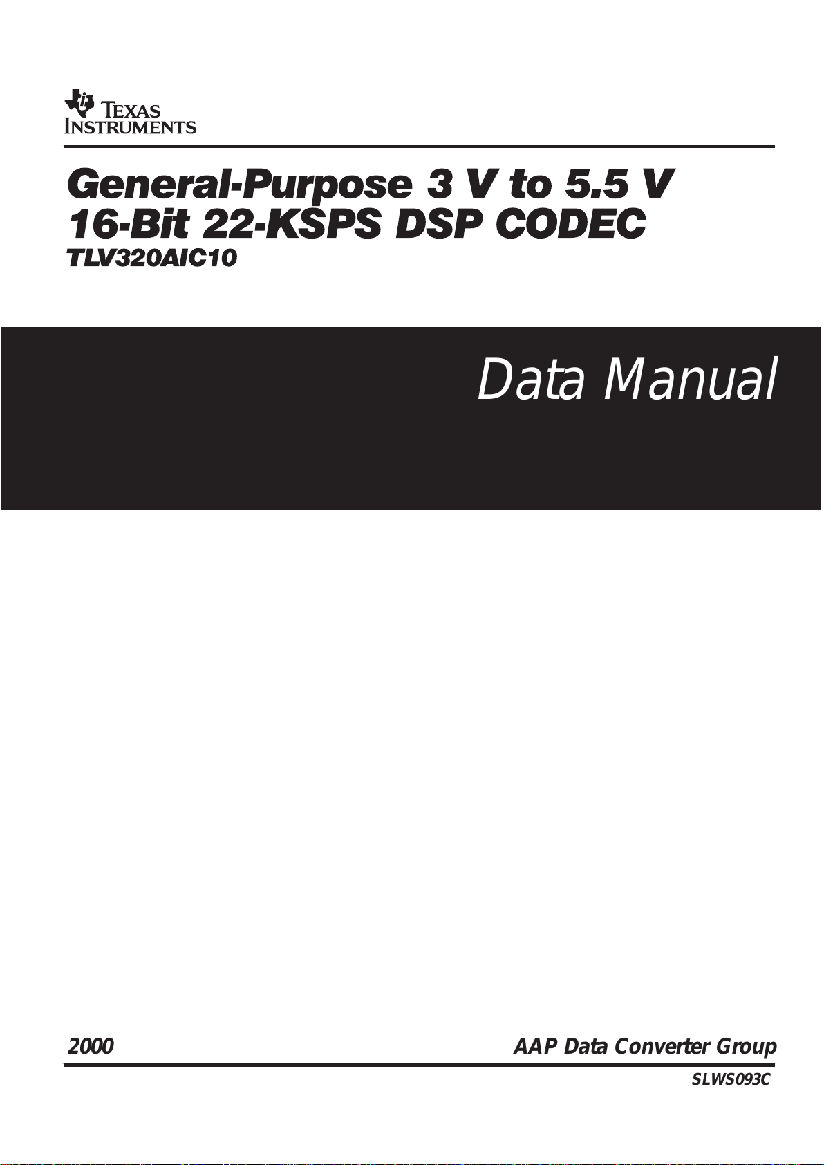
1.2 Functional Block Diagram
Sigma–
Delta
ADC
Sync
Filter
Low
Pass
Filter
Sigma–
Delta
DAC
ADREFP
ADREFM
MCLK
Interface
Circuit
Div
256xN
DIN
M/S
FSD
FS
SCLK
M0
M1
OUTP
OUTM
PGA
PGA
DOUT
Internal Clock Circuit
FIR
Filter
Analog
Loopback
Decimation Filter
Anti–
Aliasing
Filter
VMID
@ 5 mA
Vref
ALTI
FLAG
FC
DCSI
DAREFP
DAREFM
MUX
AURXM
AURXFP
INM
INP
AURXCP
1.5 V
or
2.5V
DTXOP
DTXIM
Receiver or MIC Amp
Transmitter Amp
DTXIP
DTXOM
+
–
+
–
–
+
A3
A4
A2
A1
Sync
Filter
FIR
Filter
Interpolation Filter
Digital
Loopback
1–4
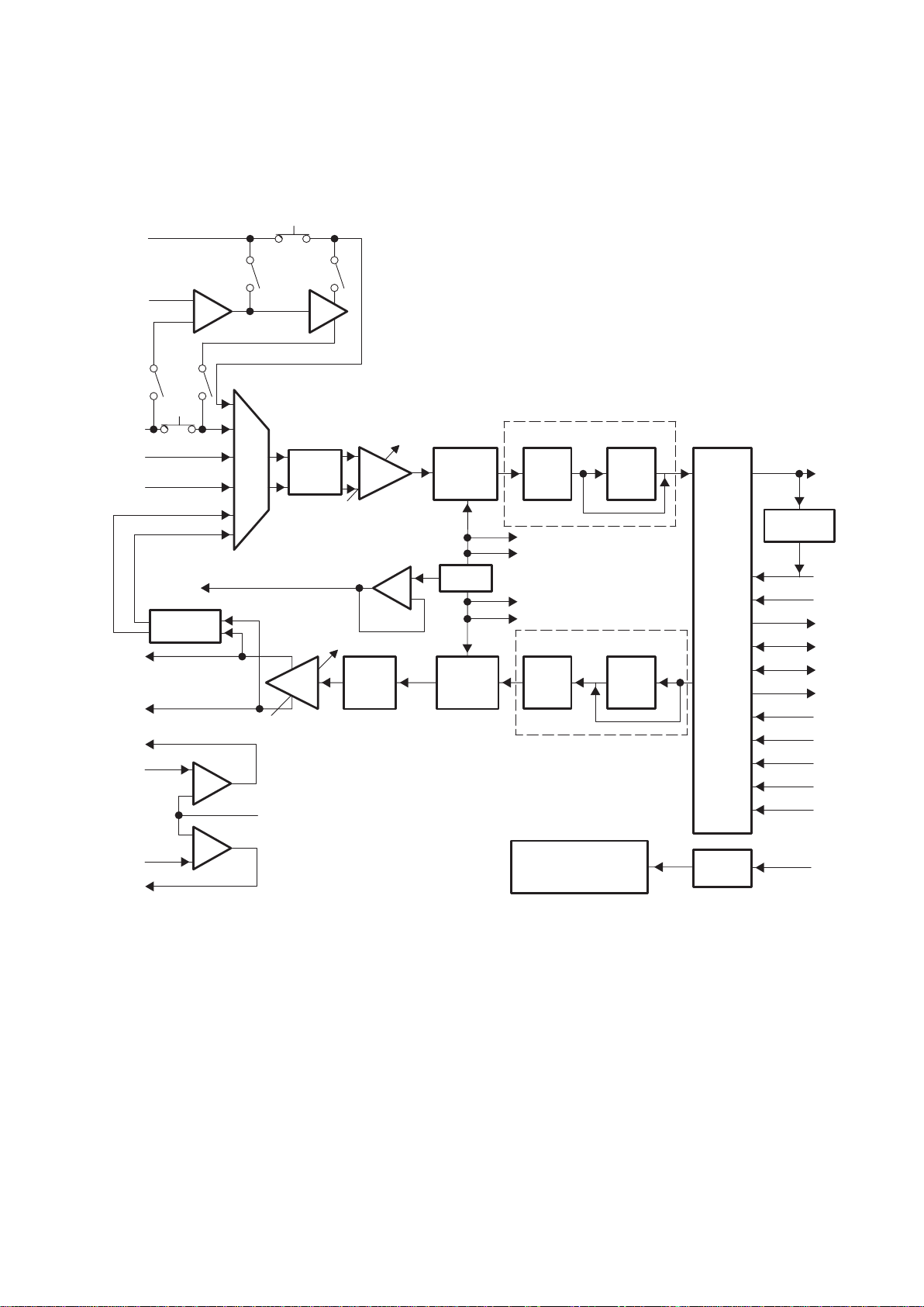
1.3 Terminal Assignments
14 15
NC
NC
AV
DD2
AV
SS
NC
NC
DV
DD2
DV
SS
NC
M/S
ALTIN
DCSI
36
35
34
33
32
31
30
29
28
27
26
25
16
1
2
3
4
5
6
7
8
9
10
11
12
AURXFP
AURXM
AURXCP
DTXOP
DTXOM
DTXIP
DTXIM
OUTP
OUTM
M0
M1
PWRDWN
17 18 19 20
FILT
47 46 45 44 4348 42
INM
INPAVAV
NC
FS
FLAG
FC
DV
DIN
NC
SCLK
MCLK
FSD
40 39 3841
21
22 23 24
37
13
NC
VMID
DV
RESET
DOUT
PFB PACKAGE
(TOP VIEW)
SS
DD1
DD1
SS
SS
AV
NC
SS
AV
NC
NOTE: All NC pins should be left unconnected.
1.4 Ordering Information
PACKAGE
T
A
48-TQFP PFB
0°C to 70°C TLV320AIC10C
–40°C to 85°C TLV320AIC10I
1.5 Terminal Functions
TERMINAL
NAME NO.
I/O
DESCRIPTION
ALTIN 26 I Serial input in the
event monitor
mode
AURXCP 3 I Receiver-path/GP amplifier noninverting input. It needs to be connected to AVSS if not used.
AURXM 2 I Receiver-path amplifier A1 inverting input, or inverting input to auxiliary analog input. It needs to be connected to
AVSS if not used. Can also be used for general-purpose amplification.
AURXFP 1 I Receiver-path amplifier A1 feedback, or noninverting input to auxiliary analog input. It needs to be connected to
AVSS if not used. Can also be used for general-purpose amplification.
AV
DD1
AV
DD2
45
34
I Analog ADC power supply
AV
SS
33, 40,
42, 46
I Analog ground
DCSI 25 I Direct configuration serial input for directly programming of internal control registers
DIN 17 I Data input. DIN receives the DAC input data and register data from the external digital signal processor (DSP),
and is synchronized to SCLK and FS. Data is latched at the falling edge of SCLK when FS is low. DIN is at high
impedance when FS is not activated.
DOUT 16 O Data output. DOUT transmits the ADC output bits and registers data, and is synchronized to SCLK and FS. Data is
sent out at the rising edge of SCLK when FS is low. DOUT is at high impedance when FS is not activated.
1–5
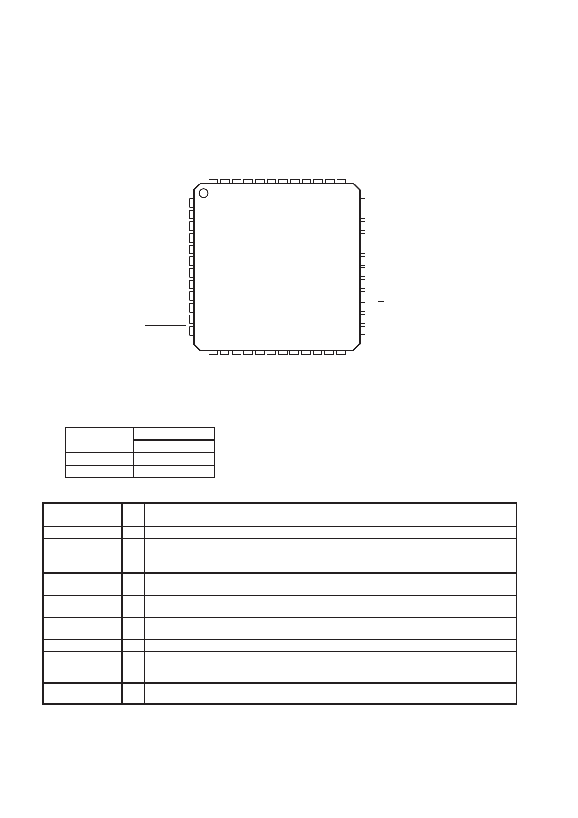
1.5 Terminal Functions (Continued)
TERMINAL
NAME NO.
I/O
DESCRIPTION
DTXIM 7 I Transmitter-path amplifier A3 analog inverting input. Can also be used for general-purpose amplification.
DTXIP 6 I Transmitter-path amplifier A4 analog noninverting input. Can also be used for general-purpose amplification.
DTXOM 5 O Transmitter path amplifier A4 feedback for negative output. Can also be used for general-purpose
amplification.
DTXOP 4 O Transmitter path amplifier A3 feedback for positive output. Can also be used for negative output.
DV
DD1
15 I Digital power supply
DV
DD2
30 I Digital power supply
DV
SS
14, 29 I Digital ground
FC 24 I Hardware request for secondary communication
FILT 38 O Bandgap filter. FILT is provided for decoupling of the bandgap reference, and provides 2.5 V. The optimal
capacitor value is 0.1 µF (ceramic). This voltage node should be loaded only with a high-impedance dc load.
FLAG 23 O Controlled by bit D4 of control register 3. If D4=0 (default), the FLAG pin outputs the communication flag that
goes low/high to indicate primary-communication/secondary-communication interval, respectively. If D4=1,
the FLAG pin outputs the value of D3.
FS 22 I/O Frame sync. When FS goes low, DIN begins receiving data bits and DOUT begins transmitting data bits. In
master mode, FS is internally generated and is low during data transmission to DIN and from DOUT . In slave
mode, FS is externally generated.
FSD 21 O Frame-sync delayed output. The FSD output synchronizes a slave device to the frame sync of the master
device. FSD is applied to the slave FS input and has the same duration as the master FS signal. Requires a
pullup resistor if not used.
INM 48 I Inverting input to analog modulator. INM requires an external R-C antialias filter with low output impedance if
the internal antialias filter is bypassed.
INP 47 I Noninverting input to analog modulator. INP requires an external R-C antialias filter with low output impedance
if the internal antialias filter is bypassed.
M0 10 I Combine with M1 to select serial interface mode (frame-sync mode)
M1 11 I Combine with M0 to select serial interface mode (frame-sync mode)
MCLK 20 I Master clock. MCLK derives the internal clocks of the sigma-delta analog interface circuit.
M/S 27 I Master/slave select input. When M/S is high, the device is the master, and when is low, it is a slave.
NC 18, 28, 31,
32, 35, 36,
37, 39, 41,
44
No connection
OUTM 9 O DAC’s inverting output. OUTM is functionally identical with and complementary to OUTP.
OUTP 8 O DAC’s noninverting output. OUTP can also be used alone for single-ended operation.
PWRDWN 12 I Power down. When PWRDWN is pulled low, the device goes into a power-down mode, the serial interface is
disabled, and most of the high-speed clocks are disabled. However, all register values are sustained and the
device resumes full-power operation without reinitialization when PWRDWN is pulled high again. PWRDWN
resets the counters only and preserves the programmed register contents. See paragraph 2.2.2 for more
information.
RESET 13 I Reset. The reset function is provided to initialize all the internal registers to their default values. The serial port
can be configured to the default state accordingly. See Appendix A,
Register Set
, and Subsection 2.2.1,
Reset
and Power-Down Functions
for detailed descriptions.
SCLK 19 I/O Shift clock. SCLK signal clocks serial data into DIN and out of DOUT during the frame-sync interval. When
configured as an output (M/S
high), SCLK is generated internally by multiplying the frame-sync signal
frequency by 256 (cascade devices < 5) or 512 (cascade devices > 4). When configured as an input (M/S low),
SCLK is generated externally and must be synchronous with the master clock and frame sync.
VMID 43 O Reference voltage output at A VDD/2

1–6
1.6 Definitions and Terminology
Data transfer interval The time during which data is transferred from DOUT to DIN. The interval is 16 shift clocks and the
data transfer is initiated by the falling edge of the FS signal.
Signal data This refers to the input signal and all of the converted representations through the ADC channel, and
the signal through the DAC channel to the analog output. This is in contrast with the purely-digital
software control data.
Primary
communication
Primary communication refers to the digital data-transfer interval. Since the device is synchronous,
the signal data words from the ADC channel and to the DAC channel occur simultaneously.
Secondary
communication
Secondary communication refers to the digital control and configuration data-transfer interval into
DIN, and the register read-data cycle from DOUT . The data transfer occurs when requested by hard-
ware or software.
SPI Serial peripheral interface standard set by Motorola
Frame/pulse sync Frame/pulse sync refers only to the falling edge of the signal FS that initiates the data-transfer inter-
val. The primary FS starts the primary communication, and the secondary FS starts the secondary
communication.
Frame/pulse sync and
sampling period
Frame/pulse sync and sampling period is the time between falling edges of successive primary FS
signals and it is always equal to 256xSCLK if the number of cascading devices is less than 5, or 512
xSCLK if the number of cascading devices is greater than 4.
f
s
The sampling frequency
ADC channel ADC channel refers to all signal-processing circuits between the analog input and the digital
conversion result at DOUT.
DAC channel DAC channel refers to all signal-processing circuits between the digital data word applied to DIN and
the differential output analog signal available at OUTP and OUTM.
Host A host is any processing system that interfaces to DIN, DOUT, SCLK, FS, and/or MCLK.
Dxx Bit position in the primary data word (xx is the bit number).
DSxx Bit position in the secondary data word (xx is the bit number).
d The alpha character
d
represents valid programmed or default data in the control-register format
(see Section 3.2,
Secondary Serial Communication
) when discussing other data bit portions of the
register.
PGA Programmable gain amplifier
FIR Finite-duration impulse response
DCSI Direct configuration serial interface for host control
1.7 Register Functional Summary
There are five control registers which are used as follows:
Register 0 The no-op register . Addressing register 0 allows secondary-communication request without altering any
other registers.
Register 1 Control register 1. The data in this register has the following functions:
• Produce the output flag to indicate a decimator FIR filter overflow (read cycle only)
• Enable of general-purpose operational amplifiers A1, A3, and A4
• Enable/bypass ADC’s analog antialiasing filter
• Select normal or auxiliary analog input
• Control 16-bit or (15+1)-bit mode of DAC operation
• Enable/bypass the decimator FIR filter
• Enable/bypass the interpolator FIR filter

1–7
Register 2 Control register 2. The data in this register has the following functions:
• Control of the low-power mode that converts data at the rate of 8 ksps
• Control of the N-divide register that determines the filter clock rate and sample period
Register 3 Control register 3. The data in this register has the following functions:
• Software reset and power down
• Selection of analog loopback, digital loopback, and event monitor mode
• Control of continuous data transfer mode
• Control of the value of one-bit general-purpose output flag
• Control the output of FLAG pin
• Enable/disable ADC path
• Enable/disable DAC path
• Control of 16-bit or (15+1)-bit mode of ADC operation
Register 4 Control register 4. The data in this register has the following functions:
• Control of the 4-bit gain of input amplifier
• Control of the 4-bit gain of output amplifier

1–8
2–1
2 Functional Description
2.1 Device Functions
2.1.1 Operating Frequencies
The sampling frequency represented by the frequency of the primary communication is derived from the master clock
(MCLK) input with the following equation:
Fs = Sampling (conversion) frequency = MCLK/(256 × N), N = 1, 2..., 32
The inverse of the sampling frequency is the time between the falling edges of two successive primary frame-sync
signals. This time is the conversion period. For example, to set the conversion rate to 8 kHz, MCLK = 256 × N × 8000.
NOTE: The value of N is defined in control register 2 and its power-up value is 32.
2.1.2 ADC Signal Channel
Both IN (INP, INM) and AUX (AURXFP, AURXM) inputs can use the built-in antialiasing filter that can be bypassed
by writing a 1 to bit D5 of control register 1. The AUX input can also be connected to the general-purpose amplifier
A1 for general-purpose applications, such as electret-microphone interface and 2-to-4-wire hybrid interface, by
writing a 1 to bit D6 of control register 1. Bit D4 of control register 1 selects between IN or AUX for the ADC. The
selected input signal is amplified by the PGA and applied to the ADC input. The ADC converts the signal into
discrete-output digital words in 2s-complement data format, corresponding to the analog-signal value at sampling
time. These 16-bit (or 15-bit) digital words, representing sampled values of the analog input signal after PGA, are
clocked out of the serial port (DOUT) at the positive edge of SCLK during the frame-sync (FS) interval at the rate of
one bit for each SCLK and one word for each primary communication. During secondary communication, the data
previously programmed into the registers can be read out. If a register read is not required, all 16 bits are cleared to
0 in the secondary communication. This read operation is accomplished by sending the appropriate register address
(D1 1-D9) with the read bit (D12) set to 1 during present secondary communication. The timing sequence is shown
in Figures 2–1 and 2–2.
The decimation FIR filter can be bypassed by writing a
1
to bit D2 of control register 1. The whole ADC channel can
be turned off for power savings by writing
01
to bits D2 and D1 of control register 3.
D0
16 SCLKs
SCLK
FS
DOUT
(16-bit)
DOUT
(15+1-bit)
D1
MSB LSB
LSB
D15
M/SD1
0 1 15 16
MSB
D15
D14
D14
……
……
……
……
NOTES: A. M/S is used to indicate whether the 15-bit data comes from a master or a slave device (master: M/S=1, slave: M/S=0).
B. The MSB (D15) is stable (the host can latch the data in at this time) at the falling edging of SCLK number 0; the last bit (D0,M/S)
is stable at the falling edging of SCLK number 15.
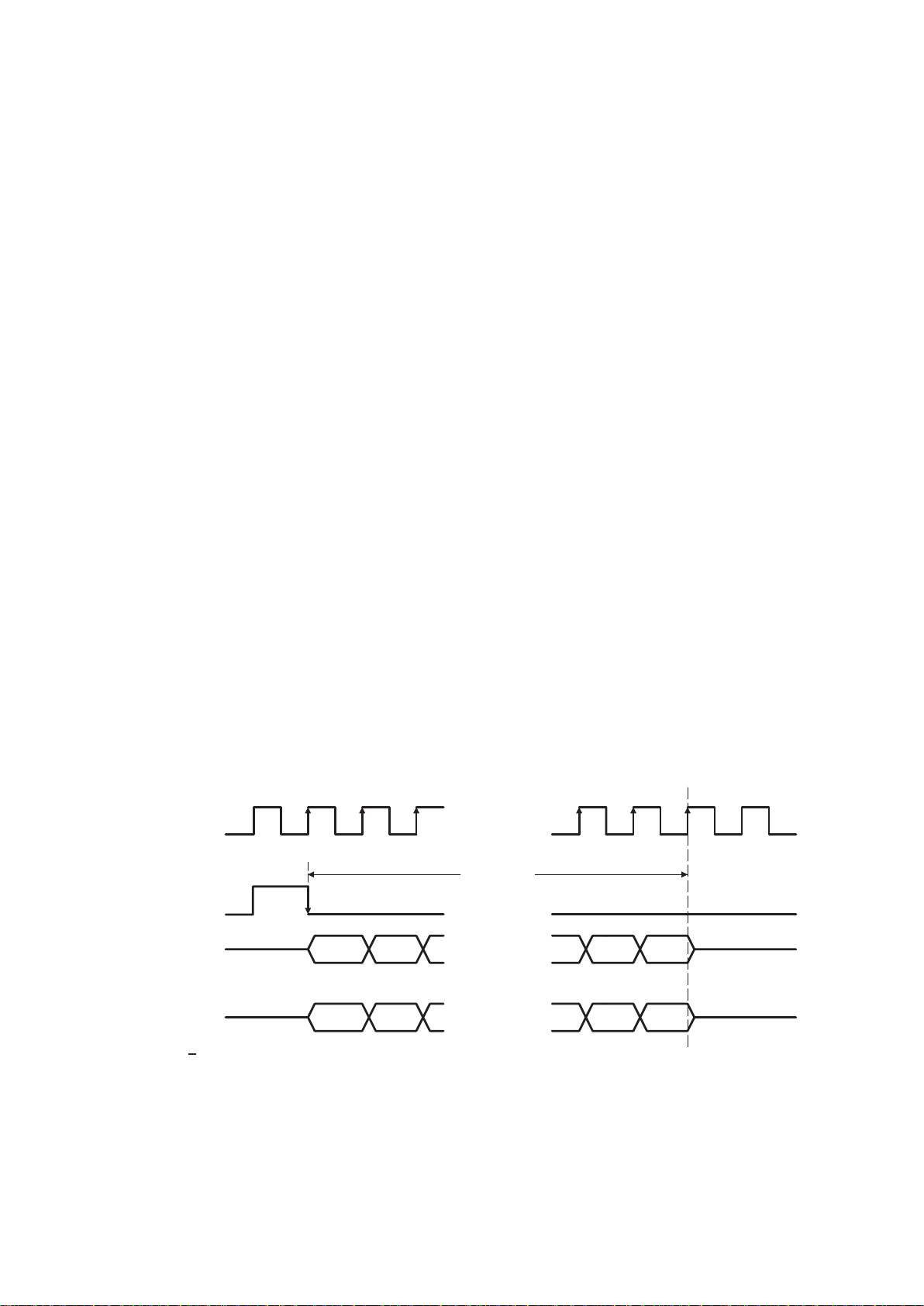
Figure 2–1. Timing Sequence of ADC Channel (Primary Communication Only)

2–2
FS
DOUT
(16-bit)
DOUT
(15+1-bit)
Primary Secondary
16 SCLKs
# SCLKs Per Sampling Period (See Note C)
16–bit ADC Data
15–bit ADC Data + M/S
M/S+ Register Data/
M/S+ All 0 (See Note A)
# SCLKs (See Note B)
M/S+ Register Data/
M/S+ All 0 (See Note A)
Primary
16 SCLKs
NOTES: A. M/S bit (D15) in the secondary communication is used to indicate whether the register data (address and content) come from a
master device or a slave device if read bit is set. Otherwise, it is all 0s except M/S bit (master: M/S=1, slave: M/S=0).
B. The number of SCLKs between FS (primary) and FS (secondary) is 128 if cascading devices are less than 5, or 256 if cascading
devices are greater than 4.
C. The number of SCLKs per data sampling period is 256 if cascading devices are less than 5, or 512 if cascading devices are greater
than 4.
Figure 2–2. Timing Sequence of ADC Channel (Primary and Secondary Communication)
2.1.3 DAC Signal Channel
DIN received the 16-bit serial data word (2s complement) from the host during the primary communication interval.
These 16-bit digital words, representing analog output signal before PGA, are clocked into the serial port (DIN) at
the falling edge of SCLK during the frame-sync interval, one bit for each SCLK and one word for each primary
communication interval. The data are converted to a pulse train by the sigma-delta DAC comprised of a
digital-interpolation filter and a digital 1-bit modulator. The output of the modulator is then passed to an internal
low-pass filter to complete the signal reconstruction. Finally, the resulting analog signal applied to the input of a
programmable-gain amplifier is capable of differentially driving a 600-ohm load at OUTP and OUTM. The timing
sequence is shown in Figure 2–3.
During secondary communication, the digital control and configuration data, together with the register address, are
clocked in through DIN (see Appendix A for register map). These 16-bit data are used either to initialize the register
or read out register content through DOUT . If a register initialization is not required, a no-operation word (D15-D9 are
all set to 0) can be used. If D12 is set to 1, the content of the control register, specified by D7-D0, will be sent out
through DOUT during the same secondary communication (see section 2.1.5). The timing sequence is shown in
Figure 2–4.
The interpolation FIR filter can be bypassed by writing a
1
to bit D1 of control register 1. The whole DAC channel can
be turned off for power savings by writing 10 to bits D2 and D1 of control register 3.
2–3
D0
16 SCLKs
SCLK
FS
DIN
(16-bit)
DIN
(15+1-bit)
D1
MSB LSB
LSB
D15
D0=0D1
0 1 15 16
MSB
D15
D14
D14
……
……
……
……
14
(See Note A)
NOTE A: d0 = 0 means no secondary-communication request (software secondary-request control, see Section 3.2).
Figure 2–3. Timing Sequence of DAC Channel (Primary Communication Only)
FS
DIN (16-bit)
(See Note A)
DIN
(15+1-bit)
Primary Secondary
16 SCLKs
# SCLKs Between Sampling Period (See Note D)
16–bit DAC Data
# SCLKs Between
Primary
16 SCLKs
FS (Primary) and
FS (Secondary)
(See Note C)
15–bit DAC Data +
D0 = 1 (See Note B)
Register Read/Write
Register Read/Write
NOTES: A. FC has to be set high for a secondary communication request when 16-bit DAC data format is used (see Section 3.2).
B. D0 = 1 means secondary communication request (software secondary request control, see Section 3.2)
C. The number of SCLKs between FS (Primary) and FS (Secondary) is 128 if cascading devices are less than 5, or 256 if cascading
devices are greater than 4.
D. The number of SCLKs per data sampling period is 256 if cascading devices are less than 5, or 512 if cascading devices are greater
than 4.
Figure 2–4. Timing Sequence of DAC Channel (Primary and Secondary Communication)
2–4
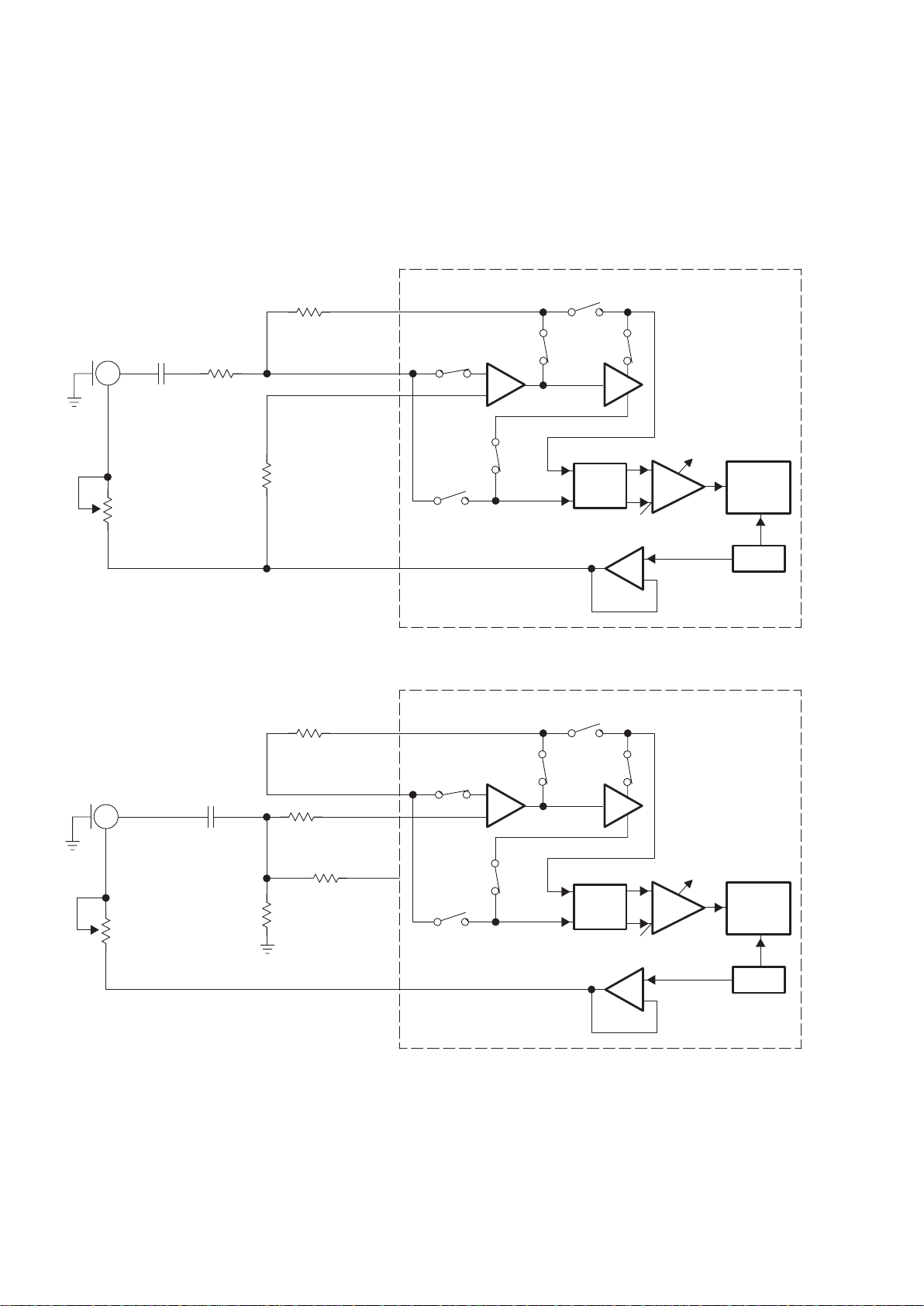
2.1.4 MIC Input
The auxiliary inputs (AURXFP, AURXCP, and AURXM) can be programmed to interface with a microphone such as
an electret microphone, as illustrated in Figure 2.5, by writing a 1 to both bit D6 and bit D4 of control register 1.
Sigma-
Delta
ADC
PGA
TLV320AIC11
Anti-
Aliasing
Filter
Vref
AURXFP
Electret
Microphone
MIC_BIAS VMID
10 kΩ
AURXM
AURXCP
20 kΩ
S2D
+
–
1 kΩ
Sigma-
Delta
ADC
PGA
TLV320AIC11
Anti-
Aliasing
Filter
Vref
AURXFP
Electret
Microphone
MIC_BIAS VMID
1 µF
20 kΩ
10 kΩ
AURXM
AURXCP
10 kΩ
10 kΩ
S2D
+
–
AVDD
1 kΩ
10 kΩ
0.1 µF
(a) Inverting Configuration
(b) Noninverting Configuration
Figure 2–5. Typical Microphone Interface

2–5
2.1.5 Antialiasing Filter
The built-in antialiasing filter has a 3-dB cutoff frequency of 70 kHz.
2.1.6 Sigma-Delta ADC
The sigma-delta analog-to-digital converter is a sigma-delta modulator with 128× oversampling. The ADC provides
high-resolution, low-noise performance using oversampling techniques. Due to the oversampling employed, only
single-pole RC filters are required on the analog inputs.
2.1.7 Decimation Filter
The decimation filters reduce the digital data rate to the sampling rate. This is accomplished by decimating with a ratio
of 1:64. The output of the decimation filter is a 16-bit 2s-complement data word clocking at the sample rate selected
for that particular data channel. The BW of the filter is 0.45 × FS and scales linearly with the sample rate.
2.1.8 Sigma-Delta DAC
The sigma-delta digital-to-analog converter is a sigma-delta modulator with 128× oversampling. The DAC provides
high-resolution, low-noise performance using oversampling techniques.
2.1.9 Interpolation Filter
The interpolation filter resamples the digital data at a rate of 64 times the incoming sample rate. The high-speed data
output from the interpolation filter is then used in the sigma-delta DAC. The BW of the filter is 0.45 x FS and scales
linearly with the sample rate.
2.1.10 Analog and Digital Loopback
The analog and digital loopbacks provide a means of testing the modem data ADC/DAC channels and can be used
for in-circuit system level tests. The analog loopback routes the DAC low-pass filter output into the analog input where
it is then converted by the ADC to a digital word. The digital loopback routes the ADC output to the DAC input on the
device. Analog loopback is enabled by writing
01
to bits D7 and D6 respectively in control register 3. Digital loopback
is enabled by writing 10 to bits D7 and D6 in control register 3 (see Appendix A).
2.1.11 FIR Overflow Flag
The decimator FIR filter sets an overflow flag (bit D7) in control register 1 to indicate that the input analog signal has
exceeded the range of the internal decimation-filter calculations. When the FIR overflow flag has been set in the
register, it remains set until the register is read by the user. Reading this value resets the overflow flag.
If FIR overflow occurs, the input signal has to be attenuated either by the PGA or some other method.
2.1.12 Bypass Mode
An option is provided to bypass the FIR filter sections of the decimation and interpolation filters. This mode is selected
through bits D1 and D2 of control register 1, and effectively increases the frequency of FS signal to 4 times the normal
FIR-filter output rate. The sinc filters of the two paths can not be bypassed.

2–6
2.1.13 Automatic Cascading Detection (ACD)
The TLV320AIC10’s ACD makes cascade programming easy and supports the operation of up to eight devices in
cascade. See Appendix A for register map description.
MCLK
DIN
DOUT
FS
SCLK
MCLK
DIN
DOUT
FS
SCLK
MCLK
DIN
DOUT
FS
SCLK
Slave 6 Slave 1 Slave 0Master
MCLK
DIN
DOUT
FSD
SCLK
FSD FSD
FS
CLKOUT
DX
DR
FSX
FSR
CLKX
CLKR
TMS320C5X
DVDD
FSD
M/S M/S M/S M/S
(or Master Clock Source)
DVDD
1 kΩ
Figure 2–6. Cascading
2.1.14 Low-Power Mode
To select the low-power mode, in which the AIC10 typically consumes 38.6 mW, set bit D7 of control register 2 to 1
and set the sampling rate at 8 ksps.
2.1.15 Event-Monitor Mode
This mode is only available during the register-write cycle, and is enabled by writing 11 to bits D6 and D7 of control
register 3. The event monitor mode is provided for applications that need hardware control and monitoring of external
events. By allowing the device to drive the FLAG terminal (set through bit D3 of the control register 3), the host DSP
is capable of system control through the same serial port that connects the device. Along with this control is the
capability of monitoring the value of the ALTIN terminal during a secondary communication cycle. One application
of this function is in monitoring RING DETECT or OFFHOOK DETECT from a phone-answering system. FLAG allows
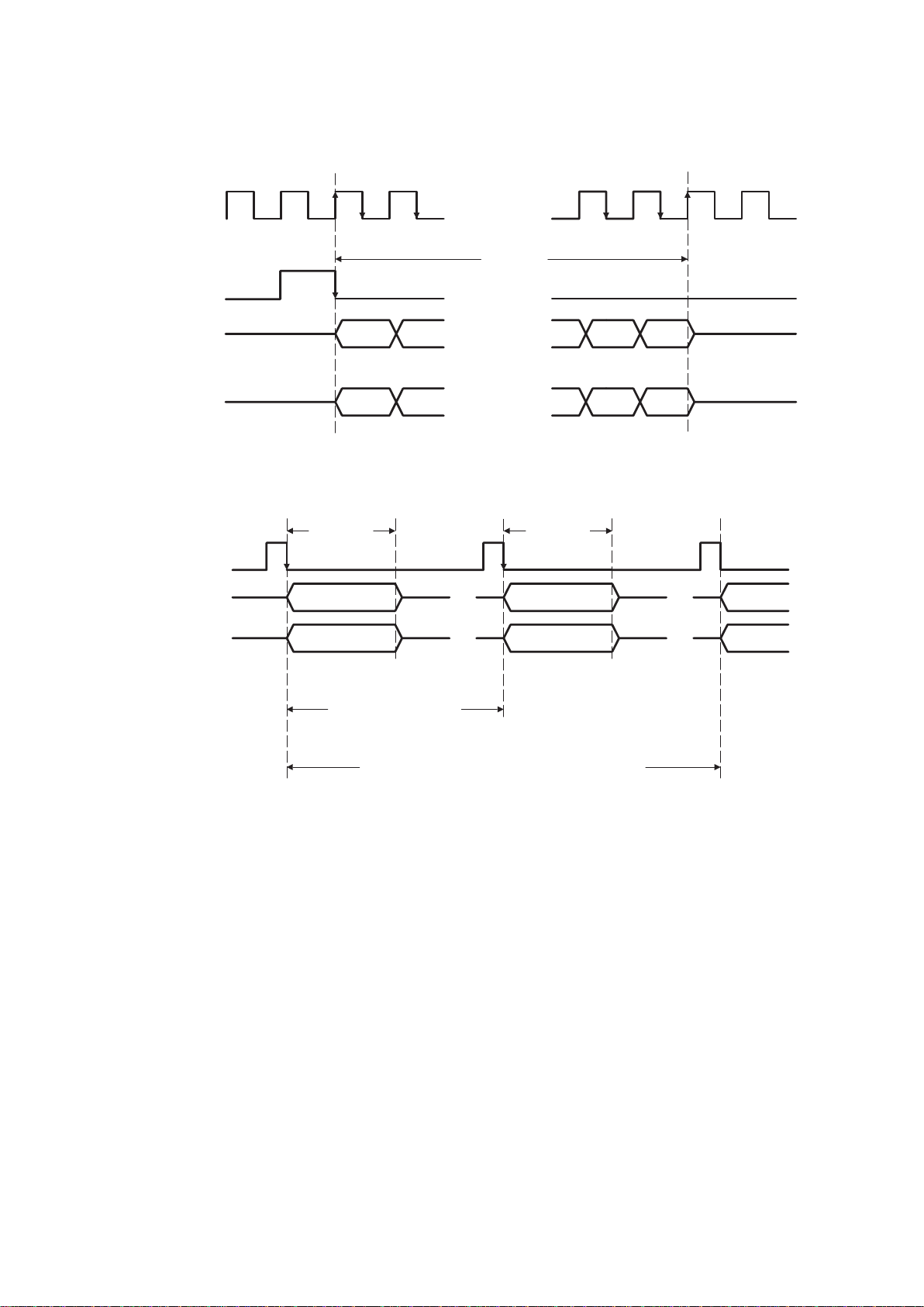
response to these incoming control signals. Figure 2–7 shows the timing associated with this operating mode.
FS
DOUT
ALTDI
Primary Secondary
16 bits
NOTE A: When DIN performs a write operation (sets D12 to 0) during secondary communication.
Figure 2–7. Event Monitor Mode Timing

2–7
2.2 Reset and Power-Down Functions
2.2.1 Software and Hardware Reset
The TLV320AIC10 resets the internal counters and registers in response to either of two events:
• A low-going reset pulse is applied to terminal RESET
• A 1 is written to the programmable-software reset bit (D3 of control register 1)
Either event resets the control registers and clears all the sequential circuits in the device. Reset signals should be
at least 6 master-clock periods long, and it is recommended to synchronize the reset signal with the master clock in
master/slave cascade. For devices in cascade, it takes at least two FS cycles to apply software reset to all devices,
with the master being always programmed last.
2.2.2 Software and Hardware Power Down
With the exception of the digital interface, the device enters the power-down mode when D1 and D2 in control register
3 are set to 1. When PWRDWN is taken low, the entire device is powered down. In either case, the register contents
are preserved and the output of the monitor amplifier is held at the midpoint voltage to minimize pops and clicks.
The amount of power drawn during software power down is higher than it is during a hardware power down because
of the current required to keep the digital interface active. Additional differences between software and hardware
power-down modes are detailed in the following paragraphs. Figure 2–8 represents the internal power-down logic.
PWRDWN
Software Power Down
(For Control Register 3, D1 & D2)
D1 and D2 are
programmed through a
secondary write operation
Internal TLV320AIC10
Figure 2–8. Internal Power-Down Logic
2.2.2.1 Software Power Down
When D1 and D2 of control register 3 are set to 1, TL V320AIC10 enters the software power-down mode. In this state,
the digital-interface circuit is still active, while the internal ADC and DAC channels and differential outputs OUTP and
OUTM are disabled, and DOUT and FSD are inactive. Register data in secondary serial communications is still
accepted, but data in primary serial communications is ignored. The device returns to normal operation when D1 and
D2 of control register 3 are reset.
2.2.2.2 Hardware Power Down
When PWRDWN is held low, the device enters the hardware power-down mode. In this state, the internal-clock
control circuit and the differential outputs OUTP and OUTM are disabled. All other digital I/Os are either disabled, or
remain in the same state they were in immediately before power down. DIN can not accept any data input. The device
can only be returned to normal operation by taking and holding PWRDWN high. When not holding the device in the
hardware power-down mode, PWRDWN
should be tied high.

2–8
2.3 Clock Source
MCLK is the external master-clock input. The clock circuit generates and distributes the necessary clocks throughout
the device. When the device is in the master mode, SCLK and FS are output and derived from MCLK in order to
provide clocking of the serial communications between the device and a DSP (digital signal processor). When in the
slave mode, SCLK and FS are all inputs. The SCLK can be connected to a faster clock source to speed up serial
communication between the slave and the master while the internal clock is maintained at 256 clocks per FS period
for internal processing. In SPI mode, the device is a slave and SCLK is connected to the SPICLK source.
2.4 Data Out (DOUT)
DOUT is placed in the high-impedance state after completing transmission of the LSB. In primary communication the
data word is the ADC conversion result. In secondary communication the data in the register read results when
requested by the read/write (R/W) bit. If a register read is not requested, the low eight bits of the secondary word are
all zeroes. The state of the master/slave (M/S) terminal is reflected by the MSB in secondary communication (DOUT ,
bit D15), and by the LSB in primary communication (DOUT, bit D0).
2.4.1 Data Out, Master Mode
In the master mode, DOUT is taken from the high-impedance state by the falling edge of the master frame-sync (FS).
The most significant data bit then appears first on DOUT.
2.4.2 Data Out, Slave Mode
In the slave mode, DOUT is taken from the high-impedance state by the falling edge of the external frame-sync (FS).
The most significant data bit then appears first on DOUT.
2.5 Data In (DIN)
In a primary communication, the data word is the input digital signal to the DAC channel. If (15+1)-bit data format is
used, the LSB (D0) is used to request a secondary communication. In a secondary communication, the data is the
control and configuration data that sets the device for a particular function (see Section 3,
Serial Communications
).
The LSB of control register 1 determines whether it is a 15-bit or a 16-bit input.
2.6 FC (Hardware Secondary Communication Request)
The FC input provides for hardware requests for secondary communications. FC works in conjunction with the LSB
of the primary data word. FC should be tied low if not used.
2.7 Frame-Sync Function for TLV320AIC10
The frame-sync signal (FS) indicates the device is ready to send or receive data. FS is an output if the M/S pin is
connected to HI (master mode), and an input if the M/S pin is connected to LO (slave mode). The output FSD is a
delay version of the first frame-sync signal (FS) that is output 32 SCLKs after the first FS, and serves as the
frame-sync input to the next slave (see Figure 2–17). The data transferred out of DOUT and into DIN begins on the
falling edge of the FS signal. It can be configured as a frame or as a pulse signal, as determined by pins M0 and M1.
In normal operation, the digital serial interface consists of the shift clock (SCLK), the frame-sync signal (FS), the
ADC-channel data output (DOUT), and the DAC-channel data input (DIN). During the primary frame-synchronization
interval, SCLK clocks the ADC channel results out through DOUT , and clocks 16-bit/(15+1) DAC data in through DIN.
During the secondary frame-sync interval, SCLK clocks the register data out through DOUT in normal operation. If
the read bit (D12) is set to 1 and the device transfers control and device parameter in through DOUT. The timing
sequence is shown in Figures 2-1, 2-2, 2-3, and 2-4.

2–9
The TLV320AIC10 has three serial-interface modes that support most modern DSP engines. This modes can be
selected by M0 and M1. In mode 0 (Figure 2–9), FS is one-bit wide and it is active high one SCLK period before the
first bit (MSB) of each data transmission. In modes 1 (Figure 2–10) and 2 (Figure 2–1 1), the TL V320AIC10 operates
as a slave to interface with an SPI master in which FS is the SPISEL that determines the sampling rate. SCLK needs
to be free-running. In mode 3 (Figure 2–12), FS is low during data transmission into DIN and DOUT.
Table 2–1. Serial Interface Modes
MODE M1 M0 FRAME SYNC (FS) FORMAT
0 0 0 Pulse mode
1 0 1 SPI_CP0 mode (SPI mode 0)
2 1 0 SPI_CP1 mode (SPI mode 1)
3 1 1 Frame mode
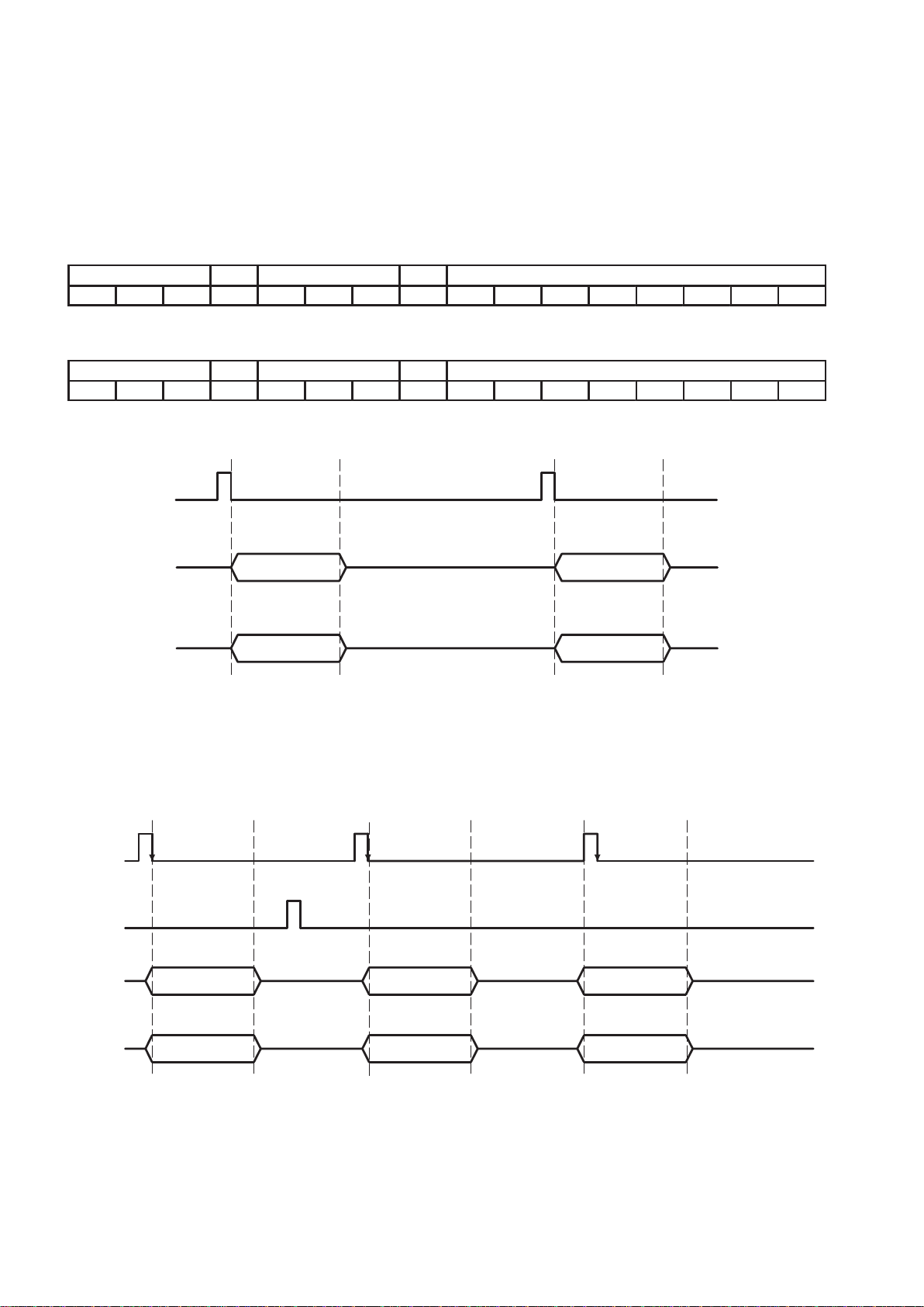
D0
16 SCLKs
SCLK
FS
DIN/DOUT
(16-bit)
D1
MSB LSB
D15
0 1 15 16
D14
……
……
……
14
Figure 2–9. Timing Diagram for the FS Pulse Mode (M1M0 = 00)
D0
16 SCLKs
(SCLK)
(FS)
DIN/DOUT
(16-bit)
D1
MSB LSB
D15
01 15
D14
……
……
……
14
SPICLK
SPISEL
Figure 2–10. Timing Diagram for the SPI_CP0 Mode (M1M0 = 01)

2–10
D0
16 SCLKs
(SCLK)
(FS)
DIN/DOUT
(16-bit)
D1
MSB LSB
D15
01 15
D14
……
……
……
14
SPICLK
SPISEL
Figure 2–11. Timing Diagram for the SPI_CP1 Mode (M1M0 = 10)
D0
16 SCLKs
SCLK
FS
DIN/DOUT
(16-bit)
D1
MSB LSB
D15
0 1 15 16
D14
……
……
……
14
Figure 2–12. Timing Diagram for the FS Frame Mode (M1M0 = 11)
NOTE: In frame mode, if AIC10 is in slave mode, DIN/DOUT should be delayed by one SCLK from the falling edge of FS.
2.7.1 Frame-Sync (FS) Function—Continuous-Transfer Mode (Master Only)
Writing a 1 to bit D5 of control register 3 enables the continuous-transfer mode. In this mode, the data bits are
transmitted and received contiguously with no inactivity between bits at the very next FS, and no further frame sync
FSs are generated. Secondary communication is not available. To disable the continuous transfer mode, use the
direct-configuration mode (See section 3.3) or reset the device.
2.7.2 Frame-Sync (FS) Function—Fast-Transfer Mode (Slave Only)
By connecting the fast clock to the SCLK pin, data can be transmitted and received at a higher rate than 256 x Fs
in the slave mode for a stand-alone AIC10.

2–11
2.7.3 Frame-Sync (FS) Function—Master Mode
The master mode in the TLV320AIC10 is selected by connecting pin M/S pin to HI. In the master mode, the
TL V320AIC10 generates the frame-sync signal (FS) to the DSP that goes low on the rising edge of SCLK and remains
low during a 16-bit data transfer.
DIN/DOUT
Primary Secondary
16 SCLKs
Primary
16 SCLKs
FS
(see Note B)
FS
(see Note A)
Primary Secondary Primary
NOTES: A. Primary and secondary serial communications
B. Primary serial communication only
Figure 2–13. Master Device Frame-Sync Signal With Primary and Secondary Communication ( No Slaves)
2.7.4 Frame-Sync (FS) Function—Slave Mode
The slave mode is selected by connecting pin M/S to LO. The frame-sync timing is generated externally by the master,
as shown in Figure 2–14 (that is, FSD) and is applied to FS of the slave to control the ADC and DAC timing.
MP
32 SCLKs
FSD (Master)
to FS (Slave)
FS
(Master to DSP)
SP MS SS MP
NOTE: MP: master primary (master-device data is transferred during this period, the DOUT of the slave device is in high-impedance state).
SP: slave primary (slave device data is transferred during this period, the DOUT of master device is in high-impedance state).
MS: master secondary (master device control register information is transferred during this period, the DOUT of slave device is in high impedance state).
SS: slave secondary (slave device control register information is transferred during this period, the DOUT of master device is in high impedance state).
Figure 2–14. Master Device’s FS Output to DSP and FSD Output to the Slave

2–12
2.7.5 Frame-Sync Delayed (FSD) Function, Cascade Mode
In cascade mode, the DSP must be able to identify the master and slaves according to the register map shown in
Appendix A. Each device in the cascade contains a 3-bit cascade register (D15-D13 in the register address) that has
been programmed by the ACD (automatic cascade detection) with an address value equal to its position in the
cascade during the device’s power-up initialization (see Section 2.1.1 1). The device address of the master is always
equal to the number of slaves in the cascade. For example, in Figure 2–15, D15-D13 of the master will be
011
, as
shown in row 4 of Table A-1 (Appendix A). The DSP receives all frame-sync pulses from the master though the
master’s FS. The master FSD is output to the first slave, and the first slave FSD is output to the second slave device,
and so on. Figure 2–15 shows the cascade of 4 TLV320AIC10s in which the closest one to the DSP is the master,
and the rest are slaves. The FSD output of each device is input to the FS terminal of the succeeding device.
Figure 2–16 shows the FSD timing sequence in the cascade.
MCLK
DIN
DOUT
FS
SCLK
MCLK
DIN
DOUT
FS
SCLK
MCLK
DIN
DOUT
FS
SCLK
Slave 2 Slave 1 Slave 0Master
MCLK
DIN
DOUT
FSD
SCLK
FSD FSD
FS
CLKOUT
DX
DR
FSX
FSR
CLKX
CLKR
TMS320C54XX
DVDD
FSD
M/S M/S M/S M/S
(or Master Clock Source)
DVDD
1 kΩ
Figure 2–15. Cascade Mode Connection (to DSP Interface)
M
32 SCLKs
Master FS
P
S2
P
S1
P
S0
P
M
S
S2
S S
Master FSD,
Slave 2 FS
Slave 2 FSD,
Slave 1 FS
Slave 1 FSD,
Slave 0 FS
Slave 0 FSD
(See Note)
32 SCLKs
32 SCLKs
32 SCLKs
NOTE: Slave 0 FSD should be left open.
Figure 2–16. Master-Slave Frame-Sync Timing

2–13
2.8 Multiplexed Analog Input and Output
The two differential analog inputs (INP and INM, or AUXP and AUXM) are multiplexed into the sigma-delta modulator .
The performance of the AUX channel is similar to the normal-input channel. The gain of the input amplifiers is set
through control register 4.
2.8.1 Multiplexed Analog Input
To produce excellent common-mode rejection of unwanted-signal performance, the analog signal is processed
differentially until it is converted to digital data. The signal applied to the INM and INP terminals should be differential
to preserve the device specifications. The signal source driving the analog inputs (INP and INM, or AUXP and AUXM)
should have a low source impedance to attain the lowest noise performance and accuracy. To obtain maximum
dynamic range, the signal should be ac-coupled to the input terminal. The analog input signal is self-biased to the
mid-supply . Bits D3 and D4 of control register 1 select these input sources. The default condition self-biases the input,
since the register default value selects INP and INM as the sources for the ADC.
TLV320AIC10
INP
V
INP
2.5 V
INM
V
INM
Figure 2–17. INP and INM Internal Self-Biased (2.5-V) Circuit
2.8.2 Analog Output
OUTP and OUTM are differential outputs and can typically drive a 600-ohm load directly. Figure 2–18 shows the
circuit when the load is ground-referenced.
–
OUTM
+
10 k Ω
10 k Ω
10 k Ω
Load
10 k Ω
+5 V
–5 V
TLE2062
OUTP
Figure 2–18. Differential Output Drive (Ground-Referenced)

2–14
2.8.3 Single-Ended Analog Input
The two differential inputs (INP and INM, or AUXP and AUXM) can be configured to work as single-ended inputs by
connecting INP or AUXP to the analog input, and INM or AUXM to the external common-mode input. This is illustrated
in Figure 2–19.
Analog Input
100 Ω
INP
INM
Common-Mode Input
C
Figure 2–19. Single-Ended Input
2.8.4 Single-Ended Analog Output
The differential output of TL V320AIC10 can be configured as a single-ended output. This is illustrated in Figure 2–20.
R
L
OUTP
OUTM
C
Figure 2–20. Single-Ended Output

3–1
3 Serial Communications
DOUT, DIN, SCLK, SXCLK, FS, and FC are the serial communication signals. SCLK is used to perform internal
processing and data transfer for serial interface between AIC10 and DSP. In the pulse/frame FS mode, there are 256
SCLKs per sampling period (512 if there are more than 4 devices in cascade). The digital-output data for the ADC
is taken from DOUT. The digital-input data for the DAC is applied to DIN. The synchronization clock for the serial
communication data and the frame-sync is taken from SCLK. The frame-sync signal that starts the ADC and DAC
data-transfer interval is taken from FS. Primary serial communication is used for signal data transmitted from the ADC
or to the DAC. Secondary communication is used to read or write words that control both the options and the circuit
configurations of the device.
The purpose of the primary and secondary communications is to allow conversion data and control data to be
transferred across the same serial port. A primary transfer is always dedicated to conversion data. A secondary
transfer or an asynchronous communication is used to set up and/or read the register values. A primary transfer
occurs for every conversion period. A secondary transfer occurs only when requested. Secondary serial
communication can be requested either by hardware (FC terminal) or by software (D0 of primary data input to DIN).
The direct configuration mode uses pin DCSI to program control registers instantly.
3.1 Primary Serial Communication
Primary serial communication is used to transmit and receive conversion signal data. The DAC word length depends
on the states of bit D0 in control register 1. After power up or reset, the device defaults to 15-bit mode. When the DAC
word length is 15 bits, the last bit of the primary 16-bit serial communication word is a control bit used to request
secondary serial communication. In the 16-bit mode, all 16 bits of the primary-communication word are used as data
for the DAC, and the hardware terminal FC must be used to request secondary communication.
Figure 3-1 shows the timing relationship for SCLK, FS, DOUT, and DIN in a primary communication. The timing
sequence for this operation is as follows:
• FS is brought low by the TLV320AIC10.
• A 16-bit word is transmitted from the ADC (DOUT), and then a 16-bit word is received from the DAC (DIN).
D0D13D15 D14 D12 D11 D10 D9 D8 D7 D6 D5 D4 D3 D2 D1
SCLK
FS
DIN
D0D13D15 D14 D12 D11 D10 D9 D8 D7 D6 D5 D4 D3 D2 D1
DOUT
Figure 3–1. Primary Serial Communication Timing

3–2
3.2 Secondary Serial Communication
Secondary serial communication is used to read or write 16-bit words that program both the options and the circuit
configurations of the device. Register programming always occurs during secondary communication. Four primary
and secondary communication cycles are requested to program the four registers. If the default value for a particular
register is desired, then the register addressing can be omitted during secondary communications. The NOOP
command addresses a pseudo-register (register 0), and no register programming takes place during this secondary
communication. If secondary communication is desired for any device (either master or slave), then a secondary
communication must be requested for all devices, starting with the master. This results in a secondary frame-sync
(FS) for all devices. The NOOP command can be used for devices that do not need a secondary operation.
During a secondary communication, a register can be written to or read from. When writing to a register, DIN contains
the value to be written. The data returned on DOUT is + 0000000000000 (3-bit device address).
There are two methods of initiating a secondary communication, as illustrated in Figure 3–2:
• Asserting a high level on FC (hardware request)
• Asserting the LSB of the DIN 16-bit serial communication high while in the 15-bit mode (software request)
NOTE:
The secondary communication request should not be asserted during the first two samples
after power up.
FC
(Hardware)
16-Bit Mode
(Control 1 Register, D0)
Internal TLV320AIC10
(LSB of DIN)
Secondary Request
Figure 3–2. Hardware and Software Secondary Communication Request
Pulling FC high causes the start of the secondary communication’s 128 or 256 SCLKs (see Figures 2–2 and 2–4)
after the start of the primary communication frame, depending on the number of devices in cascade.
The second method to initiate a secondary communication is asserting the LSB high. A software request is typically
used when the request resolution of the DAC channel is less than 16 bits. Then the least significant bit (D0) can be
used for secondary requests, as shown in Table 3–1. The request is made by placing the device in the 15-bit DAC
mode and making the LSB of DIN high. All devices should be in 15-bit DAC mode, and secondary communication
should be requested for all devices.
Table 3–1. Least Significant Bit Control Function
CONTROL BIT D0 CONTROL BIT FUNCTION
0 No operation (NOOP)
1 Secondary communication request

3–3
3.2.1 Register Programming
All register programming occurs during secondary communication through DIN or ALTI, and data are latched and
valid on the falling edge of the SCLK during the frame-sync signal. If the default value of a particular register is desired,
that register does not need to be addressed during the secondary communication interval. The no-op command
(DS15-DS8 all set to 0) addresses the pseudo-register (register 0), and no register programming takes place during
the communication.
In addition, each register can be read back through DOUT during secondary communications by setting the read bit
(D12) to 1. When a register is in the read mode, no data can be written to the register during this cycle. A subsequent
secondary communication is required to return this register to the write mode.
For example, if the contents of control register 1 of device 3 are desired to be read out from DOUT, the following
procedure must be performed through DIN:
• Request secondary communication by setting either D0 = 1(software request), or FC = high (hardware
request) during the primary communication interval.
• During the secondary communication interval (FS), send data in through DIN using the following format:
Device Address RW Register Address X Register Content
0 1 1 1 0 0 1 x x x x x x x x x
DS15 DS0
• Then, during the same frame, the following data will be read from DOUT ; the last 8 bits of DOUT will contain
register 1 data.
Device Address RW Register Address X Register Content
0 1 1 x x x x x d d d d d d d d
DS15 DS0
Figure 3–3 is the timing diagram of this procedure.
DOUT
PS
DIN
Register 1 Read
FS
Low 8 Bit (D0 – D7) is
the content of register 1
Figure 3–3. Device 3/Register 1 Read Operation Timing Diagram
3–4
To program control register 1, the following procedure must be performed through DIN:
• Request secondary communication by setting either D0=1(software request), or FC = high (hardware
request) during the primary communication interval.
• At the secondary communication interval (FS), send data in the following format through DIN:
Device Address RW Register Address X Register Content
0 1 1 0 0 0 1 x d d d d d d d d
DS15 DS0
• The following is the data out of DOUT.
Device Address RW Register Address X Register Content
0 1 1 0 x x x x 0 0 0 0 0 0 0 0
DS15 DS0
Figure 3–4 is the timing diagram of this procedure.
DOUT
PS
DIN
Register Write
FS
(Device Addr) + All 0
Figure 3–4. Device 3/Register 1 Write Operation Timing Diagram
3.2.2 Hardware Secondary Serial Communication Request
A secondary communication can be requested by asserting an FC pulse that sets an internal flag. This flag will be
reset as soon as the programming of control registers is finished. Thus, one FC pulse needs to be asserted per
secondary communication request. Figures 3–5 and 3–6 show the FS output from a master device.
DIN
FS
Primary Secondary Primary
FC
Secondary
Request
No Secondary
Request
DAC Data In
Register
Read/Write
DAC Data In
DOUT
ADC Data Out
Register
Read/Write
ADC Data Out
Figure 3–5. FS Output When Hardware Secondary Serial Communication
Is Requested Only Once (No Slave)

3–5
M
Master FS
P
S2
P
S1
P
S0
P
M
S
S2
S S
FC
(See Note)
S1
S
S0
M
P
FC pulse needs to be inserted any time
within the primary communication
NOTES: A. FC of master device and slave devices should be connected together
B. Primary communication interval = 256 SCLKs if cascading devices < 5
C. Primary communication interval = 512 SCLKs if cascading devices > 4
Figure 3–6. Output When Hardware Secondary Serial Communication Is Requested (Three Slaves)
3.2.3 Software Secondary Serial Communication Request
The LSB of the DAC data within a primary transfer can request a secondary communication through bit D0 of control
register 1 when the device is in the 15-bit mode.
For all serial communications, the most significant bit is transferred first. For a 16-bit ADC word and a 16-bit DAC word,
D15 is the most significant bit and D0 is the least significant bit. For a 15-bit DAC data word in a primary
communication, D15 is the most significant bit, D1 is the least significant bit. Bit D0 is then used for the secondary
communication request control. All digital data values are in 2s-complement data format (see Figure 3–7).
If the data format is set to 16-bit word, all 16 bits are either ADC or DAC data, and secondary communication can
only be requested by hardware (FC terminal), or control registers can be programmed by the direct configuration
mode.
PS
DIN
Register
FS
No Secondary
Communication Request
Data (D0 = 1)
Read/Write
P
Data (D0 = 0)
Secondary
Communication Request
Figure 3–7. FS Output During Software Secondary Serial Communication Request (No Slave)
3.3 Direct Configuration Mode
For DSP applications that use continuous data transfer mode for autobuffering, or for DMA operations that do not
have the capability to interfere with the data conversion channel by inserting the secondary communication, the
TLV320AIC10’s direct-configuration mode provides a flexible alternative to programming control registers through
pin DCSI. The serial input to DCSI should normally be in a high state, start its valid data with a start bit of logic low,
and pull high as a stop bit after transmission of the LSB. DCSI requires a pullup resistor for 3-state input. The AIC10
registers data bits on the falling edge of SCLK. Figure 3–8 shows a typical connection between the C54x and the
AIC10 using DCSI for direct configuration of control registers. Figure 3–9 shows the timing diagram for the direct
configuration mode.

3–6
TMS320C54XX TLV320AIC10
DCSI
M/S
FSDFS
DIN
DOUT
SCLK
DVDD
TLV320AIC10
DCSI
M/S
FS
DIN
DOUT
SCLK
DGND
DX0
FSX1
FSR1
DX1
DR1
CLKX1
CLKR1
CLKX0
DVDD
1 kΩ
TMS320C5402 TLV320AIC10
MCLK
DCSI
FSD
FS
DIN
DOUT
SCLK
Host Processor
SDO
CLKIN
BFSX0
BFSR0
BDX0
BDR0
BCLKX0
BCLKR0
DVDD
1 kΩ
MCLK
M/S
DVDD
(Use Pullup Resistor if
SDO Is 3-State Serial Bus)
(a) Direct Configuration Between C54 and AIC10
(b) Direct Configuration for Host Interface
Figure 3–8. Direct Configuration
FSD
DVDD
1 kΩ
DVDD
1 kΩ

3–7
D0D13D15 D14 D12 D11 D10 D9 D8 D7 D6 D5 D4 D3 D2 D1
SCLK
DCSI
Start Bit
= 0
Device
Address
Register
Address
Register Data Stop Bit
= 1
Figure 3–9. Direct Configuration Mode Timing
To program control register 1 of device 3, send data in with the following format through DCSI:
SB Device Address Register Address X Register Content
0 0 1 1 0 0 1 x x x x x x x x x
D15 D0
3.4 Continuous Data Transfer Mode
In continuous data transfer mode, the 16-bit converter data are transferred contiguously with no inactivity between
bits. This mode is available in the stand-alone master with M1M0 = 00 (FS-pulse mode) and selected by setting bit
D5 of control register 3 to 1. The frame sync pulse overlaps the last bit transmitted in the previous 16 bits of data.
The secondary communication request is not allowed in this mode and therefore the direct configuration mode should
be used to program the internal control registers. The continuous data transfer mode is designed to support the TI
DSP McBSP’s autobuffering unit (ABU) operation in which serial port interrupts are not generated with each word
transferred to prevent CPU’s ISR overheads.
D15 D14 D13 D12 D11 D10 D9 D8 D7 D6 D5 D4 D3 D2 D1 D0
D15 D14 D13 D12 D11 D10 D9 D8 D7 D6 D5 D4 D3 D2 D1 D0
SCLK
FS
DIN
DOUT
E15 E13 E12
E15 E14 E13 E12
E14C0
C0
Figure 3–10. Continuous Data Transfer Mode Timing

3–8
3.5 DIN and DOUT Data Format
3.5.1 Primary Serial Communication DIN and DOUT Data Format
DIN
(15 + 1)-Bit Mode
A/D & D/A Data
Secondary
Communication
Request
D15 – D1 D0
DOUT
(15 + 1)-Bit Mode
M/S Bit
D15 – D1 D0
DIN
16-Bit Mode
A/D & D/A Data
D15 – D0
DOUT
16-Bit Mode
D15 – D0
Figure 3–11. Primary Communication DIN and DOUT Data Format
3.5.2 Secondary Serial Communication DIN and DOUT Data Format
0
D8D15 D14 D13 X X X X D7 – D0
D8D15 D14 D13 1 D11 D10 D9 D7 – D0
DIN (Read)
Register Address
Don’t CareReserved
R/WDevice Address
D8D15 D14 D13 D11 D10 D9 D7 – D0
DIN (Write)
Data to the
Register
Device Address
DOUT (Read)
Register Data
Figure 3–12. Secondary Communication DIN and DOUT Data Format
3.5.3 Direct Configuration DCSI Data Format
0 D12
Register AddressDevice Address
D8D14 D13 D1 1 D10 D9 D7 – D0
DCSI (Write)
Data to the
Register
Figure 3–13. Direct Communication DCSI Data Format

4–1
4 Specifications
4.1 Absolute Maximum Ratings Over Operating Free-Air Temperature Range
(Unless Otherwise Noted)
†
Supply voltage range, DVDD, AVDD (see Note 1) –0.3 V to 7 V. . . . . . . . . . . . . . . . . . . . . . . . . . . . . . . . . . . . . . .
Output voltage range, all digital output signals –0.3V to DVDD+0.3 V. . . . . . . . . . . . . . . . . . . . . . . . . . . . . . . . . . .
Input voltage range, all digital input signals –0.3V to DVDD +0.3 V. . . . . . . . . . . . . . . . . . . . . . . . . . . . . . . . . . . .
Case temperature for 10 seconds: package 260°C. . . . . . . . . . . . . . . . . . . . . . . . . . . . . . . . . . . . . . . . . . . . . . . . . .
Operating free-air temperature range, T
A
–40°C to 85°C. . . . . . . . . . . . . . . . . . . . . . . . . . . . . . . . . . . . . . . . . . . . .
Storage temperature range, T
stg
–65°C to 150°C. . . . . . . . . . . . . . . . . . . . . . . . . . . . . . . . . . . . . . . . . . . . . . . . . . . .
†
Stresses beyond those listed under “absolute maximum ratings” may cause permanent damage to the device. These are stress ratings only and
functional operation of the device at these or any other conditions beyond those indicated under “recommended operating conditions” is not
implied. Exposure to absolute-maximum-rated conditions for extended periods may affect device reliability.
NOTE 1: All voltage values are with respect to VSS.
4.2 Recommended Operating Conditions
MIN NOM MAX UNIT
Analog supply voltage, A V
DD
3 5.5 V
Digital supply voltage, DV
DD
3 5.5 V
Analog signal peak-to-peak input voltage, V
I(analog)
(5 V supply), single-ended. 3 V
Analog signal peak-to-peak input voltage, V
I(analog)
(3.3 V supply), single-ended. 2 V
Differential output load resistance, R
L
600 Ω
Output load capacitance, C
L
20 pF
Divider N = Even 40
Master clock
Divider N = Odd 20
MH
z
ADC or DAC conversion rate 22 kHz
Operating free-air temperature, T
A
–40 85 °C
4.3 Electrical Characteristics Over Recommended Operating Free-Air Temperature
Range, AV
DD
= 5 V/3.3 V, DVDD = 5 V/3.3 V
4.3.1 Digital Inputs and Outputs, Fs = 8 kHz, Output Not Loaded
PARAMETER TEST CONDITIONS MIN TYP MAX UNIT
V
OH
High-level output voltage, DOUT IO = -360 µA 2.4 DVDD+0.5 V
V
OL
Low-level output voltage, DOUT IO = 2 mA DVSS–0.5 0.4 V
I
IH
High-level input current, any digital input VIH = 5 V 10 µA
I
IL
Low-level input current, any digital input VIL = 0.6 V 10 µA
C
i
Input capacitance 10 pF
C
o
Output capacitance 10 pF

4–2
4.3.2 ADC Path Filter, Fs = 8 kHz (see Note 2)
PARAMETER TEST CONDITIONS MIN TYP MAX UNIT
0 Hz to 300 Hz –0.5 0.2
300 Hz to 3 kHz –0.5 0.25
3.3 kHz –0.5 0.3
Filter gain relative to gain at 1020 H
z
3.6 kHz –3
dB
4 kHz –35
≥ 4.4 kHz –74
NOTE 2: The filter gain outside of the passband is measured with respect to the gain at 1024 Hz. The analog input test signal is a sine wave with
0 dB = 4 V
I(PP)
as the reference level for the analog input signal. The pass band is 0 to 3600 Hz for an 8-kHz sample rate. This pass
band scales linearly with the sample rate.
4.3.3 ADC Dynamic Performance, Fs = 8 kHz
4.3.3.1 ADC Signal-to-Noise (see Note 3)
PARAMETER TEST CONDITIONS MIN TYP MAX UNIT
VI = –1 dB 78 84
VI = –3 dB 76 81
SNR
Signal-to-noise ratio
VI = –9 dB 72 78
dB
VI = –40 dB 37 42
NOTE 3: The test condition is a 1020-Hz input signal with an 8-kHz conversion rate. Input and output common mode is 2.5 V for 5-V supply , and
1.5-V for 3.3-V supply.
4.3.3.2 ADC Signal-to-Distortion (see Note 3)
PARAMETER TEST CONDITIONS MIN TYP MAX UNIT
VI = –1 dB 76 80
VI = –3 dB 76 80
THD
Signal-to-total harmonic distortion
VI = –9 dB 80 85
dB
VI = –40 dB 64 72
NOTE 3: The test condition is a 1020-Hz input signal with an 8-kHz conversion rate. Input and output common mode is 2.5 V for 5-V supply , and
1.5-V for 3.3-V supply.
4.3.3.3 ADC Signal-to-Distortion + Noise (see Note 3)
PARAMETER TEST CONDITIONS MIN TYP MAX UNIT
VI = –1 dB 76 80
VI = –3 dB 74 79
THD+N
Signal-to-total harmonic distortion
+
noise
VI = –9 dB 72 78
dB
VI = –40 dB 38 43
NOTE 3: The test condition is a 1020-Hz input signal with an 8-kHz conversion rate. Input and output common mode is 2.5 V for 5-V supply , and
1.5-V for 3.3-V supply.

4–3
4.3.4 ADC Channel Characteristics
PARAMETER TEST CONDITIONS MIN TYP MAX UNIT
V
I(PP)
Peak-to-peak input voltage (differential) Preamp gain = 0 dB 4 V
Dynamic range VI = –3 dB 82 dB
Intrachannel isolation 87 dB
E
G
Gain error VI = –1 dB at 1020 Hz 0.6 dB
E
O(ADC)
ADC converter offset error ±15 mV
CMRR Common-mode rejection ratio at INM, INP or AUXM, AUXP VI = –1 dB at 1020 Hz 80 dB
Idle channel noise (on-chip reference) V
INP,INM
= 0 V 25 70 µVrms
R
j
Input resistance TA = 25°C 35 kΩ
Channel delay 17/f
s
s
4.3.5 DAC Path Filter, Fs = 8 kHz (see Note 4)
PARAMETER TEST CONDITIONS MIN TYP MAX UNIT
0 Hz to 300 Hz –0.5 0.2
300 Hz to 3 kHz –0.65 0.25
3.3 kHz –0.75 0.3
Filter gain relative to gain at 1020 H
z
3.6 kHz –3
dB
4 kHz –35
≥ 4.4 kHz –74
NOTE 4: The filter gain outside of the passband is measured with respect to the gain at 1020 Hz. The input signal is the digital equivalent of a
sine wave (digital full scale = 0 dB). The nominal differential DAC channel output with this input condition is 6 V
I(PP)
. The pass band
is 0 to 3600 Hz for an 8-kHz sample rate. This pass band scales linearly with the conversion rate.
4.3.6 DAC Dynamic Performance
4.3.6.1 DAC Signal-to-Noise When Load is 600 Ω (see Note 5)
PARAMETER TEST CONDITIONS MIN TYP MAX UNIT
VI = 0 dB 80 85
VI = –3 dB 78 84
SNR
Signal-to-noise ratio
VI = –9 dB 72 78
dB
VI = –40 dB 35 42
NOTE 5: The test condition is the digital equivalent of a 1020 Hz input signal with an 8-kHz conversion rate. The test is measured at output of
application schematic low-pass filter. The test is conducted in 16-bit mode.
4.3.6.2 DAC Signal-to-Distortion when load is 600 Ω. (see Note 5)
PARAMETER TEST CONDITIONS MIN TYP MAX UNIT
VI = 0 dB 70 77
VI = –3 dB 78 85
THD
Signal-to-total harmonic distortion
VI = –9 dB 78 85
dB
VI = –40 dB 62 66
NOTE 5: The test condition is the digital equivalent of a 1020 Hz input signal with an 8-kHz conversion rate. The test is measured at output of
application schematic low-pass filter. The test is conducted in 16-bit mode.

4–4
4.3.6.3 DAC Signal-to-Distortion + Noise When Load is 600 Ω (see Note 5)
PARAMETER TEST CONDITIONS MIN TYP MAX UNIT
VI = 0 dB 70 77
VI = –3 dB 73 78
THD+N
Signal-to-total harmonic distortion
+
noise
VI = –9 dB 70 78
dB
VI = –40 dB 35 42
NOTE 5: The test condition is the digital equivalent of a 1020 Hz input signal with an 8-kHz conversion rate. The test is measured at output of
application schematic low-pass filter. The test is conducted in 16-bit mode.
4.3.7 DAC Channel Characteristics
PARAMETER TEST CONDITIONS MIN TYP MAX UNIT
Dynamic range VI = 0 dB at 1020 Hz 82 dB
Interchannel isolation 100 dB
E
G
Gain error, 0 dB VO = 0 dB at 1020 Hz 0.5 dB
Idle channel narrow band noise 0 kHz to 4 kHz, See Note 6 25 70 µVrms
V
OO
Output offset voltage at OUT (differential) DIN = all zeros 30 mV
p
5 V
Differential with respect to common mode
–4 4
VOAnalog output voltage
3.3 V
Differential with res ect to common mode
and full-scale digital input
–2.5 2.5
V
Channel delay 18/f
s
NOTE 6: The conversion rate is 8 kHz.
4.3.8 Op-Amp Interface (A1, A3, A4)
PARAMETER TEST CONDITIONS MIN TYP MAX UNIT
A
V
Gain 100
Input voltage range 0.5 AVDD –
0.5
V
Input offset voltage 10 mV
Input offset current 0 mA
Output power 15 mW
SNR Signal-to-noise ratio Input frequency = 1020 Hz 90 dB
THD + N Signal-to-total harmonic distortion + noise Input frequency = 1020 Hz 90 dB
Unity-gain bandwidth Open loop 10 MHz
Noise output voltage 30 µVrms
4.3.9 Power-Supply Rejection (see Note 7)
PARAMETER TEST CONDITIONS MIN TYP MAX UNIT
AV
DD
Supply-voltage rejection ratio, analog supply fj = 0 to fs/2 75 dB
pp
DAC channel
95
DVDDSuppl
y-v
oltage rejection ratio
ADC channel
f
j
= 0 to 30 kHz
86
dB
NOTE 7: Power supply rejection measurements are made with both the ADC and the DAC channels idle and a 200 mV peak-to-peak signal
applied to the appropriate supply .

4–5
4.3.10 Power Supply
4.3.10.1Low-Power Mode (set control register bit D7 to 1)
PARAMETER TEST CONDITIONS MIN TYP MAX UNIT
P
D
Power dissipation All sections on, VDD = 3.3 V 39.3 mW
pp
All sections on, AVDD = 3.3 V 9.7 mA
I
DD
(analog)
Supply current
All sections on, AVDD = 5 V 11.2 mA
pp
All sections on, AVDD = 3.3 V 2.3 mA
I
DD
(digital)
Supply current
All sections on, AVDD = 5 V 4.9 mA
4.3.10.2Normal Operation
PARAMETER TEST CONDITIONS MIN TYP MAX UNIT
P
D
Power dissipation All sections on, VDD = 3.3 V 48.5 mW
All sections on, AVDD = 3.3 V 13.6 mA
pp
All sections on, AVDD = 5 V 14.8 mA
I
DD
(analog)
Supply current
Power down, AVDD = 3.3 V 3 µA
Power down, AVDD = 5 V 11 µA
All sections on, AVDD = 3.3 V 1.1 mA
pp
All sections on, AVDD = 5 V 2.3 mA
I
DD
(digital)
Supply current
Power down, AVDD = 3.3 V 0.15 mA
Power down, AVDD = 5 V 0.6 mA
4.4 Timing Requirements (see
Parameter Measurement Information
)
4.4.1 Master Mode Timing Requirements
PARAMETERS TEST CONDITIONS MIN TYP MAX UNIT
t
d1
Delay time, SCLK↑ to FS↓ 5 ns
t
d2
Delay time, SCLK↑ to DOUT 15 ns
t
su1
Setup time, DIN, before SCLK low 5 ns
t
h1
Hold time, DIN, after SCLK high 1/2T+5 ns
t
en1
Enable time, FS↓ to DOUT 1/2T+5 ns
t
dis1
Disable time, FS↑ to DOUT Hi-Z
CL = 20 pF
5 ns
t
d3
Delay time, MCLK↓ to SCLK↑ 10 ns
t
d(CH-FL)
Delay time, SCLK high to FS/FSD high (see Figure 5-1) 5 ns
t
d(CH-FH)
Delay time, SCLK high to FS/FSD high 5 ns
t
wH
Pulse duration, MCLK high 12.5 ns
t
wL
Pulse duration, MCLK low 12.5 ns

4–6

5–1
5 Parameter Measurement Information
SCLK
FS/FSD
t
d(CH–FL)
0.8 V
2.4 V
t
d(CH–FH)
Figure 5–1. FS and FSD Timing
MCLK
SCLK
FS
DOUT
DIN
t
d3
t
d1
t
wL
t
wH
t
en1
t
h1
t
su1
D15
D15 D14
D14
t
d2
t
dls
Figure 5–2. Serial Communication Timing
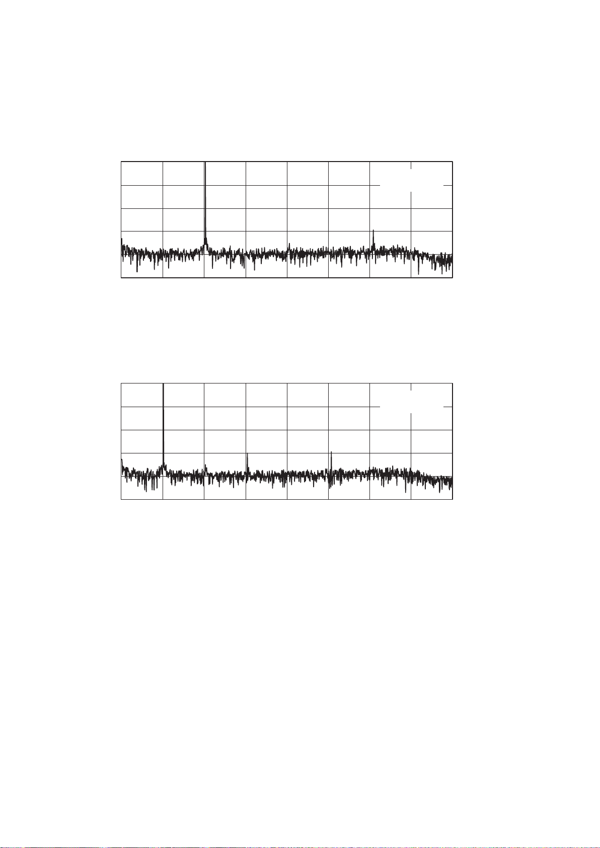
5–2
–150
–120
–90
–60
–30
0
0 500 1000 1500 2000 2500 3000 3500 4000
AMPLITUDE
vs
FREQUENCY
f – Frequency – Hz
fs = 8 kHz
Input = –3 dB
Amplitude – dB
Figure 5–3. FFT–ADC Channel, fs = 8 kHz, Input = –3 dB
–150
–120
–90
–60
–30
0
0 1000 2000 3000 4000 5000 6000 7000 8000
AMPLITUDE
vs
FREQUENCY
f – Frequency – Hz
fs = 16 kHz
Input = –3 dB
Amplitude – dB
Figure 5–4. FFT–ADC Channel, fs = 16 kHz, Input = –3 dB

5–3
–150
–120
–90
–60
–30
0
0 500 1000 1500 2000 2500 3000 3500 4000
AMPLITUDE
vs
FREQUENCY
f – Frequency – Hz
fs = 8 kHz
Input = –3 dB
Amplitude – dB
Figure 5–5. FFT–DAC Channel, fs = 8 kHz, Input = –3 dB
–150
–120
–90
–60
–30
0
0 1000 2000 3000 4000 5000 6000 7000 8000
AMPLITUDE
vs
FREQUENCY
f – Frequency – Hz
fs = 16 kHz
Input = –3 dB
Amplitude – dB
Figure 5–6. FFT–DAC Channel, fs = 16 kHz, Input = –3 dB

5–4
–150
–120
–90
–60
–30
0
0 500 1000 1500 2000 2500 3000 3500 4000
AMPLITUDE
vs
FREQUENCY
f – Frequency – Hz
fs = 8 kHz
Input = –1 dB
Amplitude – dB
Figure 5–7. FFT–ADC Channel, fs = 8 kHz, Input = –1 dB
–150
–120
–90
–60
–30
0
0 1000 2000 3000 4000 5000 6000 7000 8000
AMPLITUDE
vs
FREQUENCY
f – Frequency – Hz
fs = 16 kHz
Input = –1 dB
Amplitude – dB
Figure 5–8. FFT–ADC Channel, fs = 16 kHz, Input = –1 dB

5–5
–150
–120
–90
–60
–30
0
0 500 1000 1500 2000 2500 3000 3500 4000
AMPLITUDE
vs
FREQUENCY
f – Frequency – Hz
fs = 8 kHz
Input = –0 dB
Amplitude – dB
Figure 5–9. FFT–DAC Channel, fs = 8 kHz, Input = 0 dB
–150
–120
–90
–60
–30
0
0 1000 2000 3000 4000 5000 6000 7000 8000
AMPLITUDE
vs
FREQUENCY
f – Frequency – Hz
fs = 16 kHz
Input = –0 dB
Amplitude – dB
Figure 5–10. FFT–DAC Channel, fs = 16 kHz, Input = 0 dB

5–6

6–1
6 Mechanical Information
PFB (S-PQFP-G48) PLASTIC QUAD FLATPACK
4073176/B 10/96
Gage Plane
0,13 NOM
0,25
0,45
0,75
Seating Plane
0,05 MIN
0,17
0,27
24
25
13
12
SQ
36
37
7,20
6,80
48
1
5,50 TYP
SQ
8,80
9,20
1,05
0,95
1,20 MAX
0,08
0,50
M
0,08
0°–7°
NOTES: A. All linear dimensions are in millimeters.
B. This drawing is subject to change without notice.
C. Falls within JEDEC MS-026

6–2

A–1
Appendix A
Register Set
Bits D15 through D13 represent the device address in the cascade set by the automatic cascade detection described
in Section 2.1.13. In cascading, the master is the device directly connected to the DSP . For example, if there are four
devices in the cascade, as shown in row 4 of T able A-1 and in Section 2.7.5, the device address D15-D13 of the master
will have a binary value of
011
. The other three slaves’ addresses are
010, 001,
and
000,
corresponding to their
positions in the cascade. The device address for a stand-alone device is always
000
. Bits D1 1 through D8 comprise
the address of the register that is written with data carried in D7 through D0. D12 determines a read or write cycle
to the addressed register; a low selects a write cycle.
The following table shows the register map.
REGISTER MAP
D15 D14 D13 D12 D11 D10 D9 D8 D7 D6 D5 D4 D3 D2 D1 D0
Device Address RW Register Address X Control Register Content
T able A–1. Device Address
D15 D0D1D2D3D4D5D6D7D8D9D10D11D12D13D14
Device Address R/W Register Adress X Register Content
Device 0
REGISTER MAP
000
000
000
000
000
000
000
000
Device 1
001
001
001
001
001
001
001
Device 2
010
010
010
010
010
010
Device 3
011
011
011
011
011
Device 4
100
100
100
100
Device 5
101
101
101
Device 6
110
110
Device 7
1118
7
6
5
4
3
1
2
DEVICE ADDRESS (D15–D13)# Devices
in Cascade
T able A–2. Register Address
REGISTER NO. D11 D10 D9 REGISTER NAME
0 0 0 0 No operation
1 0 0 1 Control 1
2 0 1 0 Control 2
3 0 1 1 Control 3
4 1 0 0 Control 4

A–2
A.1 Control Register 1
T able A–3. Register Map
D7 D6 D5 D4 D3 D2 D1 D0 DESCRIPTION
ovf – – – – – – – Decimator FIR overflow flag
– 1 – – – – – – Enable HYBRID receiver/MIC amp (A1)
– 0 – – – – – – Disable HYBRID/MIC amp (A1)
– – 1 – – – – – Bypass antialiasing filter
– – 0 – – – – – Enable antialiasing filter
– – – 1 – – – – Select AUXP and AUXM for ADC
– – – 0 – – – – Select INP and INM for ADC
– – – – 1 – – – Software reset
– – – – 0 – – – Default
– – – – – 1 – – Bypass decimation/interpolation FIR filter
– – – – – 0 – Normal operation with FIR filter
– – – – – – 1 – Enable HYBRID transmitter/MIC amps (A3,A4)
– – – – – – 0 – Disable HYBRID transmitter/MIC amps (A3,A4)
– – – – – – – 1 16-bit data format for DAC
– – – – – – – 0 15-bit data + LSB format for DAC
Default value: 00000000
NOTE: A software reset is a one-shot operation and this bit is cleared to 0 after reset. It is not necessary to write a 0 to end the
master reset operation.
A.2 Control Register 2
Table A–4. Control Register 2
D7 D6 D5 D4 D3 D2 D1 D0 DIVIDE VALUE
1 – – – – – – – Low-power operation mode
0 – – – – – – – Normal operation mode
– 1 – – – – – – S–D modulator stops
– 0 – – – – – – S–D modulator runs
– – R – – – – – Reserved
– – – 1 1 1 1 1 Frequency Divider N = 31
– – – • •
– – –
• •
– – – • •
– – – 0 0 0 0 1 Frequency Divider N = 1
– – – 0 0 0 0 0 Frequency Divider N = 32
Default value: 00000000
NOTE: The serial port interface always gluelessly works with the DSP. The following modes will not produce
50% duty cycle SCLK:
1. If the number of devices in cascade >4 and N is an odd number (i.e., N = 1, 3, 5,...)
2. If the number of devices in cascade ≤4, FIR is bypassed, and N ≠ 4, 8, 12, 16, 20, 24, 28, 32

A–3
A.3 Control Register 3
Table A–5. Control Register 3
D7 D6 D5 D4 D3 D2 D1 D0 DESCRIPTION
0 0 – – – – – – Default
0 1 – – – – – – Analog loopback enabled
1 0 – – – – – – Digital loopback enabled
1 1 – – – – – – Event-monitor mode enabled (write cycle only)
– – 1 – – – – – Continuous data-transfer mode (master only)
– – 0 – – – – – Default
– – – 1 – – – – FLAG output = D3
– – – 0 – – – – FLAG output = secondary communication flag
– – – F – – – FLAG value
– – – – – 0 0 – Default
– – – – – 0 1 – Disable ADC channel
– – – – – 1 0 – Disable DAC channel
– – – – – 1 1 – Software power-down mode
– – – – – – – 1 16-bit data format for ADC
– – – – – – – 0 Not 16-bit data format for ADC
Default value: 00000000

A–4
A.4 Control Register 4
Table A–6. Control Register 4
D7 D6 D5 D4 D3 D2 D1 D0 DESCRIPTION
1 1 1 1 – – – – ADC input PGA gain = MUTE
1 1 1 0 – – – – ADC input PGA gain = 24 dB
1 1 0 1 – – – – ADC input PGA gain = 18 dB
1 1 0 0 – – – – ADC input PGA gain = 12 dB
1 0 1 1 – – – – ADC input PGA gain = 9 dB
1 0 1 0 – – – – ADC input PGA gain = 6 dB
1 0 0 1 – – – – ADC input PGA gain = 3 dB
1 0 0 0 – – – – ADC input PGA gain = –3 dB
0 1 1 1 – – – – ADC input PGA gain = –6 dB
0 1 1 0 – – – – ADC input PGA gain = –9 dB
0 1 0 1 – – – – ADC input PGA gain = –12 dB
0 1 0 0 – – – – ADC input PGA gain = –18 dB
0 0 1 1 – – – – ADC input PGA gain = –24 dB
0 0 1 0 – – – – ADC input PGA gain = –30 dB
0 0 0 1 – – – – ADC input PGA gain = –36 dB
0 0 0 0 – – – – ADC input PGA gain = 0 dB
– – – – 1 1 1 1 DAC output PGA gain = MUTE
– – – – 1 1 1 0 DAC output PGA gain = 24 dB
– – – – 1 1 0 1 DAC output PGA gain = 18 dB
– – – – 1 1 0 0 DAC output PGA gain = 12 dB
– – – – 1 0 1 1 DAC output PGA gain = 9 dB
– – – – 1 0 1 0 DAC output PGA gain = 6 dB
– – – – 1 0 0 1 DAC output PGA gain = 3 dB
– – – – 1 0 0 0 DAC output PGA gain = –3 dB
– – – – 0 1 1 1 DAC output PGA gain = –6 dB
– – – – 0 1 1 0 DAC output PGA gain = –9 dB
– – – – 0 1 0 1 DAC output PGA gain = –12 dB
– – – – 0 1 0 0 DAC output PGA gain = –18 dB
– – – – 0 0 1 1 DAC output PGA gain = –24 dB
– – – – 0 0 1 0 DAC output PGA gain = –30 dB
– – – – 0 0 0 1 DAC output PGA gain = –36 dB
– – – – 0 0 0 0 DAC output PGA gain = 0 dB
Default value: 00000000

A–5
Sigma-
Delta
ADC
PGA
TLV320AIC10
Anti-
Aliasing
Filter
AURXCP
AURXFP
AURXM
Vref
VMID
DTXOP
DTXIM
DTXIP
DTXOM
Sigma-
Delta
DAC
PGA
Low
Pass
Filter
OUTP
OUTM
Figure A–1. Differential Configuration for Hybrid Connection

A–6
Sigma-
Delta
ADC
PGA
TLV320AIC10
Anti-
Aliasing
Filter
AURXCP
AURXFP
AURXM
Vref
VMID
DTXOP
DTXIM
DTXIP
DTXOM
Sigma-
Delta
DAC
PGA
Low
Pass
Filter
OUTP
OUTM
Figure A–2. Single-Ended Configuration of Hybrid Connection

IMPORTANT NOTICE
T exas Instruments and its subsidiaries (TI) reserve the right to make changes to their products or to discontinue
any product or service without notice, and advise customers to obtain the latest version of relevant information
to verify, before placing orders, that information being relied on is current and complete. All products are sold
subject to the terms and conditions of sale supplied at the time of order acknowledgment, including those
pertaining to warranty, patent infringement, and limitation of liability.
TI warrants performance of its semiconductor products to the specifications applicable at the time of sale in
accordance with TI’s standard warranty. Testing and other quality control techniques are utilized to the extent
TI deems necessary to support this warranty. Specific testing of all parameters of each device is not necessarily
performed, except those mandated by government requirements.
Customers are responsible for their applications using TI components.
In order to minimize risks associated with the customer’s applications, adequate design and operating
safeguards must be provided by the customer to minimize inherent or procedural hazards.
TI assumes no liability for applications assistance or customer product design. TI does not warrant or represent
that any license, either express or implied, is granted under any patent right, copyright, mask work right, or other
intellectual property right of TI covering or relating to any combination, machine, or process in which such
semiconductor products or services might be or are used. TI’s publication of information regarding any third
party’s products or services does not constitute TI’s approval, warranty or endorsement thereof.
Copyright 2000, Texas Instruments Incorporated
 Loading...