
TLV320AD12A
3.3-V INTEGRATED ADSL CODEC
SLWS088B – JULY 1999 – REVISED MARCH 2000
D
Complete Discrete Multitone (DMT)-Based
DDD
Asymmetric Digital Subscriber Line (ADSL)
Coder/Decoder (Codec) Solution
D
Complies With ANSI T1.413, Issue 2 and
ITU G.992.1
D
Supports up to 8-Mbit/s Downstream and
800-kbit/s Upstream Duplex
D
Integrated 14-Bit Converter for
Transmitter/Receiver
D
Integrated Transmit/Receive (TX/RX)
Channel Filters
D
Integrated TX/RX Attenuation/Gain
D
Integrated Reference
D
High-Speed Parallel Interface
description
The TL V320AD12A is a high-speed coder/decoder (codec) for central office-side (CO) discrete-multitone (DMT)
asymmetric-digital subscriber line (ADSL) access that supports ANSI Std T1.413, Issue 2 and ITU G.992.1. The
codec is a low-power device comprised of five major functional blocks: transmitter (TX), receiver (RX), clock,
reference, and host interface.
D
2s-Complement Data Format
D
Selectable 2.2-MSPS or 4.4-MSPS Parallel
Data Transfer Rate
D
Serial Configuration Port
D
Eight General-Purpose (GP) Output
Terminals
D
Supports Multiple-Channel Configuration
D
Single 3.3-V Supply
D
Hardware/Software Power Down
D
–40°C to 85°C Operation
D
Packaged in 100-Pin Plastic Quad Flatpack
The transmit channel consists of a 25.875-kHz to 1.104-MHz digital band-pass filter, a 14-bit, 8.832-MSPS DAC,
a 1.104-MHz analog low-pass filter, and a transmit attenuator. The receiver channel consists of a two
programmable-gain-amplifier stages (PGA), a 138-kHz analog low-pass filter, a 14-bit, 4.416-MSPS ADC, a
138-kHz digital low-pass filter. An onboard reference circuit generates 1.5-V reference voltage for the
converters.
The codec has two interface ports: a parallel port for data transfer, and a serial port for control. The parallel port
is 16 bits wide, and is reserved for moving data between the codec and a DSP, such as the TMS320C6XX.
Configuration is done via the serial port. A special interface scheme enables multichannel system design. The
TLV320AD12A can be powered down via a dedicated terminal or through software control to reduce heat
dissipation. Additionally , there is a general-purpose (GP) port consisting of eight output terminals for control of
external circuitry.
Please be aware that an important notice concerning availability, standard warranty, and use in critical applications of
Texas Instruments semiconductor products and disclaimers thereto appears at the end of this data sheet.
PRODUCTION DATA information is current as of publication date.
Products conform to specifications per the terms of Texas Instruments
standard warranty. Production processing does not necessarily include
testing of all parameters.
POST OFFICE BOX 655303 • DALLAS, TEXAS 75265
Copyright 2000, Texas Instruments Incorporated
1
TLV320AD12A
3.3-V INTEGRATED ADSL CODEC
SLWS088B – JULY 1999 – REVISED MARCH 2000
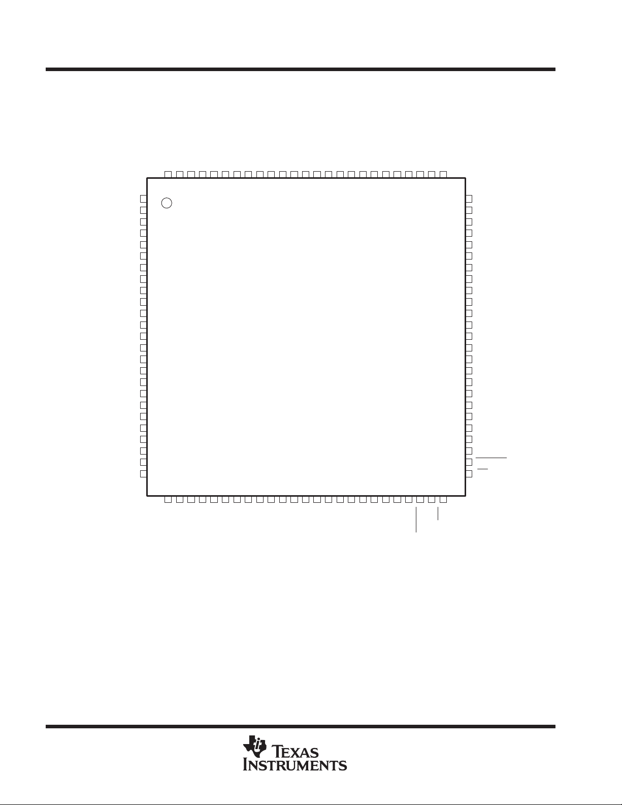
PZ PACKAGE
(TOP VIEW)
_FIL_TX
GP0
GP1
GP2
GP3
GP4
GP5
GP6
GP7
DVSS
NC
VMID_ADC
AVDD_ADC
A VSS_ADC
NC
DVDD_RX
DVSS_RX
D0
D1
D2
D3
D4
D5
D6
D7
D8
1
2
3
4
5
6
7
8
9
10
11
12
13
14
15
16
17
18
19
20
21
22
23
24
25
NC
100
26
NC
99
27
NC
98
28
NC
97
29
RXM
95
96
31
30
RXP
AVDD_FIL_RX
AVSS_FIL_RX
93
94
33
32
V
92
SS
REFM
NC
VMID_REF
89
90
91
REFP
88
TL V320AD12A
38
37
36
35
34
AVDD_REF
AVSS_REF
86
87
40
39
AVSS_FIL_TX
NC
84
85
42
41
TXM
AVDD
83
44
43
82
TXP
81
45
NC
80
46
NC
79
47
NC
78
48
NC
77
49
NC
76
75
74
73
72
71
70
69
68
67
66
65
64
63
62
61
60
59
58
57
56
55
54
53
52
51
50
NC
NC
NC
NC
AVSS2_TX
AVDD2_TX
COMPB_TX
COMPA_TX
AVSS1_TX
AVDD1_TX
NC
NC
NC
NC
NC
NC
NC
DVSS
DVDD_DAC
DVSS_DAC
ADR1
ADR0
PWDN
RESET
CS
D9
D11
D12
D10
DVDD_BF
DVSS_BF
No connection (leave open)
2
POST OFFICE BOX 655303 • DALLAS, TEXAS 75265
D13
D14
D15
SDO
SDI
FS
SCLK
INT
OSEN
CLKIN
CLKOUT
DVSS_CLK
SYNC
DVDD_CLK
DVSS_LG
DVDD_LG
NC
WETX
OE
TLV320AD12A
I/O
†
DESCRIPTION
3.3-V INTEGRATED ADSL CODEC
SLWS088B – JULY 1999 – REVISED MARCH 2000
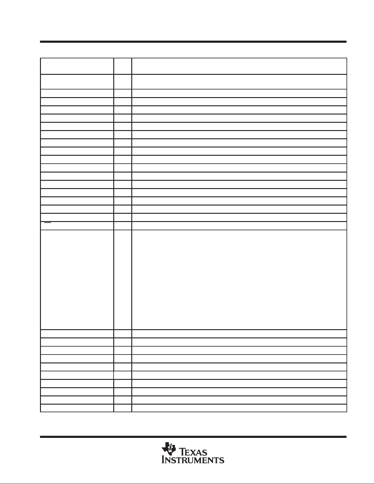
Terminal Functions
TERMINAL
NAME NO.
ADR0
ADR1
AVDD_ADC 12 I Analog-to-digital converter (ADC) analog power supply
AVDD1_TX 66 I TX-channel analog power supply 1
AVDD2_TX 70 I TX-channel analog power supply 2
AVDD_FIL_RX 93 I RX-channel filter analog power supply
AVDD_FIL_TX 83 I TX-channel filter analog power supply
AVDD_REF 86 I Reference analog power supply
AVSS_ADC 13 I ADC analog ground
AVSS1_TX 67 I TX-channel analog ground 1
AVSS2_TX 71 I TX-channel analog ground 2
AVSS_FIL_RX 94 I RX-channel filter analog ground
AVSS_FIL_TX 84 I TX-channel filter analog ground
AVSS_REF 87 I Reference analog ground
CLKIN 42 I 35.328-MHz external oscillator clock input
CLKOUT 41 O 4.416-MHz clock output
COMPA_TX 68 I TX-channel decoupling capacitor input A (add 500 pF X7R ceramic capacitor to AVDD1_TX)
COMPB_TX 69 I TX-channel decoupling capacitor input B (add 1-µF X7R ceramic capacitor to AVDD1_TX)
CS 51 I Parallel-port chip select
D15
D14
D13
D12
D11
D10
D9
D8
D7
D6
D5
D4
D3
D2
D1
D0
DVDD_BF 26 I Digital I/O buffer power supply
DVDD_CLK 44 I Digital clock power supply
DVDD_DAC 57 I Digital power supply for digital-to-analog converter (DAC)
DVDD_LG 47 I Digital logic power supply
DVDD_RX 15 I Digital power supply for RX channel
DVSS 9, 58 I Digital ground
DVSS_BF 27 I Digital I/O buffer ground
DVSS_CLK 43 I Digital clock ground
DVSS_DAC 56 I Digital ground for DAC
DVSS_LG 46 I Digital logic ground
†
I = input, O = output, I/O = 3-state input/output
54
55
34
33
32
31
30
29
28
25
24
23
22
21
20
19
18
17
I Serial-port chip ID address. ADR0 is the least significant bit.
(MSB)
Parallel-port data. D0 is the least significant bit.
I/O
(LSB)
POST OFFICE BOX 655303 • DALLAS, TEXAS 75265
3
TLV320AD12A
I/O
†
DESCRIPTION
3.3-V INTEGRATED ADSL CODEC
SLWS088B – JULY 1999 – REVISED MARCH 2000
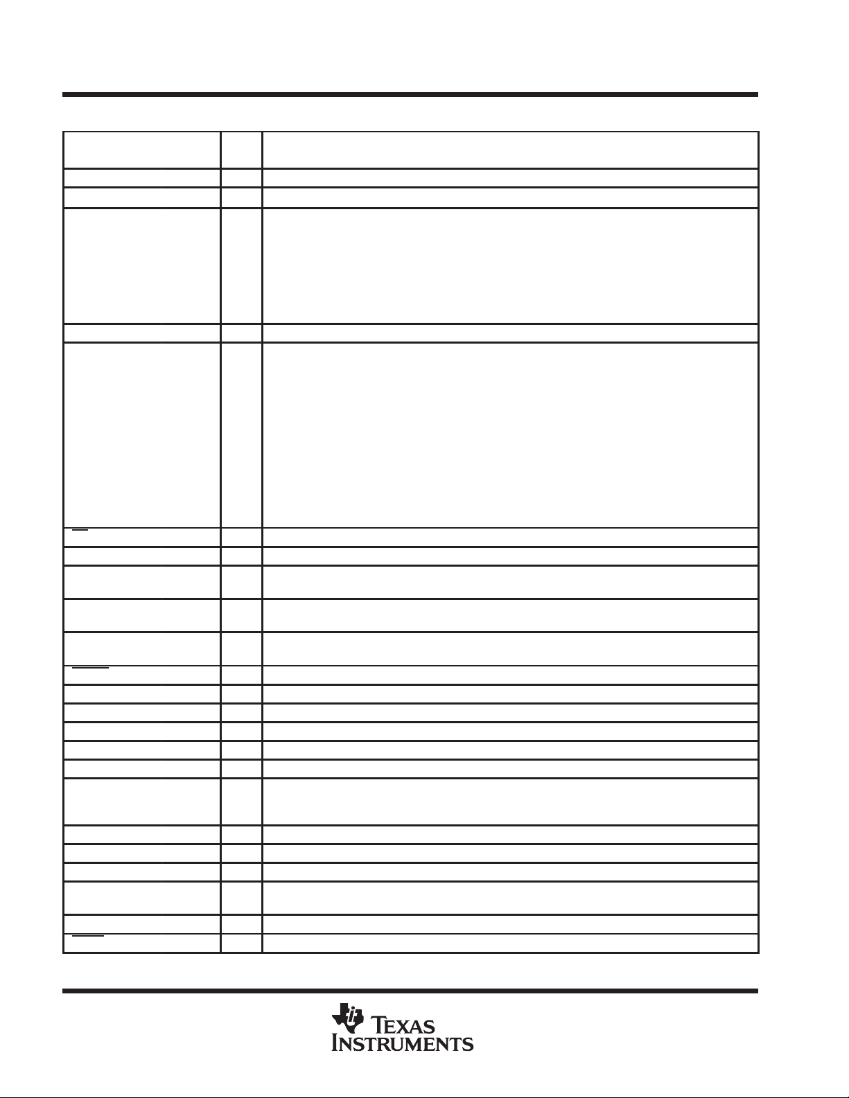
Terminal Functions (Continued)
TERMINAL
NAME NO.
DVSS_RX 16 I Digital ground for RX channel
FS 38 I Frame sync input
GP7
GP6
GP5
GP4
GP3
GP2
GP1
GP0
INT 40 O Data rate clock output (INT is 4.416 MHz when OSEN = 1, 2.208 MHz when OSEN = 0)
NC
OE 50 I Parallel-port output enable from host processor
OSEN 39 I Over-sampling enable input. OSEN = 1 enables oversampling mode (INT = 4.416 MHz)
PWDN 53 I
REFM 89 O
REFP 88 O
RESET 52 I Hardware system reset. An low level will reset the device.
RXM 96 I Receive RX input minus. RXM is self-biased to AVDD_FIL_RX/2.
RXP 95 I Receive RX input plus. RXP is self-biased to AVDD_FIL_RX/2.
SCLK 37 O Serial clock output
SDI 36 I Serial data input
SDO 35 O Serial data output
SYNC 45 I
TXM 82 O T ransmit output minus
TXP 81 O Transmit output plus
VMID_ADC 11 O Decoupling 1.5 V for ADC. Add 10-µF tantalum, and 0.1-µF X7R ceramic capacitors to A VSS_ADC.
VMID_REF 90 O
V
SS
WETX 48 I Parallel-port write enable for TX channel from host processor
†
I = input, O = output, I/O = 3-state input/output
8
7
6
5
4
3
2
1
10, 14,
49, 59,
60, 61,
62, 63,
64, 65,
72, 73,
74, 75,
76, 77,
78, 79,
80, 85,
91, 97,
98, 99,
100
92 I Substrate. Connect VSS to analog ground.
O General-purpose output port
No connection. All the NC pins should be left open.
Power-down input. When PWDN = 0, the device is in normal operating mode. When PWDN = 1, the
device is in hardware power-down mode.
Decoupling reference voltage minus. Add 10-µF tantalum and 0.1-µF X7R ceramic capacitors to
AVSS_REFP. The normal dc voltage at this terminal is 0.5 V . See figure 7 for the configuration.
Decoupling reference voltage plus. Add 10-µF tantalum and 0.1-µF X7R ceramic capacitors to
AVSS_REFM. The normal dc voltage at this terminal is 2.5 V. See figure 7 for the configuration.
SYNC pulse for clock synchronization. A high pulse to the pin synchronizes the internal clock
operation. The default state of the pin is low. Refer to Figure 3 for detail. Tie the SYNC terminal to
the DVSS_LG terminal for autosynchronization.
Decoupling 1.5 V reference voltage. Add 10-µF tantalum, and 0.1-µF X7R ceramic capacitors to
AVSS_REF.
4
POST OFFICE BOX 655303 • DALLAS, TEXAS 75265
functional block diagram
Codec
Interface
D0–D15
WETX
INT
D0–D15
OE
ADR0
ADR1
FS
SDI
SDO
SCLK
Input
Buffer
Parallel
Bus
Ouput
Buffer
Serial
Interface
2.208 MSPS
4.416 MSPS
(Over-Sampling)
2.208 MSPS
4.416 MSPS
(Over-Sampling)
Clock
Generator
1.104 MHz
Digital
LPF
138 kHz
Digital
LPF
25.875 kHz
Digital
HPF
SCR7[D0]
(Bypassed at Default)
14 Bit
4.416 MSPS
RX
ADC
Internal
Reference
3.3-V INTEGRATED ADSL CODEC
SLWS088B – JULY 1999 – REVISED MARCH 2000
14 Bit
8.832 MSPS
TX
DAC
0 to 9 dB
(1 dB/step)
RX PGA2
PGA2 PGA1
4 Vp-p
General
Purpose
Output
1.104 MHz
TX
LPF
138 KHz
RX
LPF
Control Block
TLV320AD12A
0 to –24 dB
(–1 dB/step)
TX PAA
TXP
PAA
TXM
0 to 6 dB
(1 dB/step)
RX PGA1
RXP
RXM
OSEN
CLKOUT
4.416 MHz
CLKIN
35.328 MHz
GP0–GP7
PWDN RESET SYNC
functional description
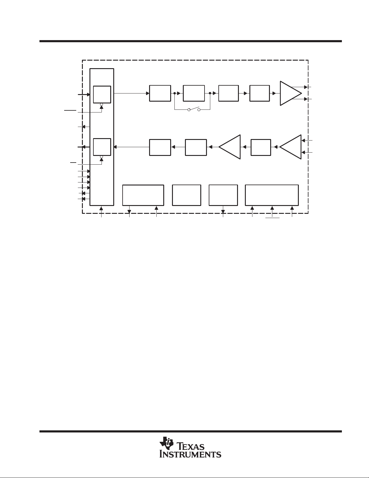
The TL V320AD12A is a low-power device consisting of transmitter, receiver , clock, reference, and host interface
(see the functional block diagram). It is designed to be paired with the TL V320AD1 1A remote terminal-side (RT)
codec.
The TLV320AD12A transmit channel consists of a 1.104-MHz digital low-pass filter (LPF), a 25.875-kHz
high-pass filter (HPF) that can be enabled, a 14-bit, 8.832-megabyte samples-per-second (MSPS) digital-toanalog converter (DAC), a 1.104-MHz analog LPF , and a programmable amplifier attenuator (P AA). The receive
channel consists of a two-stage programmable gain amplifier (PGA), a 138-kHz analog LPF, a 14-bit,
4.416-MSPS analog-to-digital converter (ADC), and a 138-kHz digital LPF. An onboard reference circuit
generates a 1.5-V reference for the converters.
transmit channel
The transmit channel contains a high-performance, 14-bit DAC that operates at an 8.832 MHz sampling rate
and provides a 4× oversampling to reduce the DAC noise. The low-pass filter limits the output of the transmitter
to 1.104 MHz. The programmable attenuator, with a range of 0 dB to 24 dB in –1-dB steps, drives the external
ADSL line driver. The TX HPF can be enabled by software control as shown in the functional block diagram.
receive channel
The receive channel contains a high-performance, 14-bit ADC that operates at a 4.416-MHz sampling rate and
provides 16x oversampling to reduce the antialiasing noise. The two PGAs reduce the dynamic-range
requirement of the high-resolution ADC. The two LPFs limit the input signal bandwidth to 138 kHz.
POST OFFICE BOX 655303 • DALLAS, TEXAS 75265
5

TLV320AD12A
3.3-V INTEGRATED ADSL CODEC
SLWS088B – JULY 1999 – REVISED MARCH 2000
functional description (continued)
clock generation
The clock generator provides the necessary clock signals for the device. The external oscillator specifications
are:
• 3.3-V supply
• 35.328 MHz, ±50 PPM
• 60/40 minimum duty cycle (50/50 is optimum)
Table 1 describes the major clocks generated internally.
Table 1. Clock Description
FREQUENCY
CLOCK
OSEN = 0 OSEN = 1
INT 2.208 4.416
CLKOUT 4.416 4.416
SCLK 4.416 4.416
(MHz)
INT
The interrupt (INT) to the host processor is 4.416 MHz when OSEN = 1 and 2.208 MHz when OSEN = 0.
CLKOUT
The 4.416-MHz clock output (CLKOUT) is synchronous with the master clock (35.328 MHz).
SCLK
The serial clock (SCLK) output, used in the serial codec interface, has a fixed frequency of 4.416 MHz and is
synchronous with the master clock (35.328 MHz).
parallel interface
The TL V320AD12A codec has a 16-bit parallel interface for TX and RX data. The input and output buffers (see
diagram) are updated at either 2.208 MSPS or 4.416 MSPS (over-sampling mode). Strobes OE and WETX
(from the host transceiver) are edge-triggered signals. Incoming data is registered on the rising edge of WETX.
Output data from the codec is enabled after the falling edge of OE
, and is disabled after the rising edge of OE.
The INT cycle time is hardware configurable for either 4.416 MHz (OSEN = 1), or 2.208 MHz (OSEN = 0).
For the 16-bit parallel data, D0 is the LSB and D15 is the MSB. The parallel TX and RX data contains 16 valid
bits. All 16 bits are used in the digital filtering.
keep-out zones (KOZs)
The last clock input (CLKIN cycle) before a transition of CLKOUT is defined as a keep-out zone (KOZ). These
zones are reserved for sampling of analog signals. All digital I/Os (except CLKIN) should be quiet during these
keep-out zones.
oversampling mode
The OSEN pin selects 2× oversampling mode (INT running at 4.416 MHz), or 1× oversampling mode (INT
running at 2.208 MHz).
serial interface
The serial port is used for codec configuration and register reading. The word length is 16 bits. Two
hardware-configuration terminals, ADR1 and ADR0, are used to configure the device identification (ID). Up to
four codecs can be identified for each common serial port.
6
POST OFFICE BOX 655303 • DALLAS, TEXAS 75265
TLV320AD12A
SCR0
0000
3.3-V INTEGRATED ADSL CODEC
SLWS088B – JULY 1999 – REVISED MARCH 2000
serial interface (continued)
The master codec (ADR[1:0] = 00) provides SCLK to the host processor. The SCLK terminals on the other
codecs are left unconnected. All the codecs in a multicodec system should be synchronized by SYNC pin so
that their SCLK signals are in phase—even though the slave’s SCLKs are not being used. This ensures proper
latching of the data to the codec.
SCLK is a continuously-running 4.416-MHz fixed-frequency clock. The clock is synchronized to the codec
internal events and CLKOUT (to the host), so the KOZs can be observed. A host DSP can drive the FS
(synchronized to the CLKOUT from codec) into the codec to initiate a 16-bit serial I/O frame.
general-purpose (GP) port
The GP port provides eight outputs. Each output is capable of delivering 0.5 mA for control of external circuitry
such as LEDs, gain control, and power down.
internal voltage reference
The built-in reference provides the needed reference voltage and current to individual analog blocks. It is also
brought out to external terminals for noise decoupling.
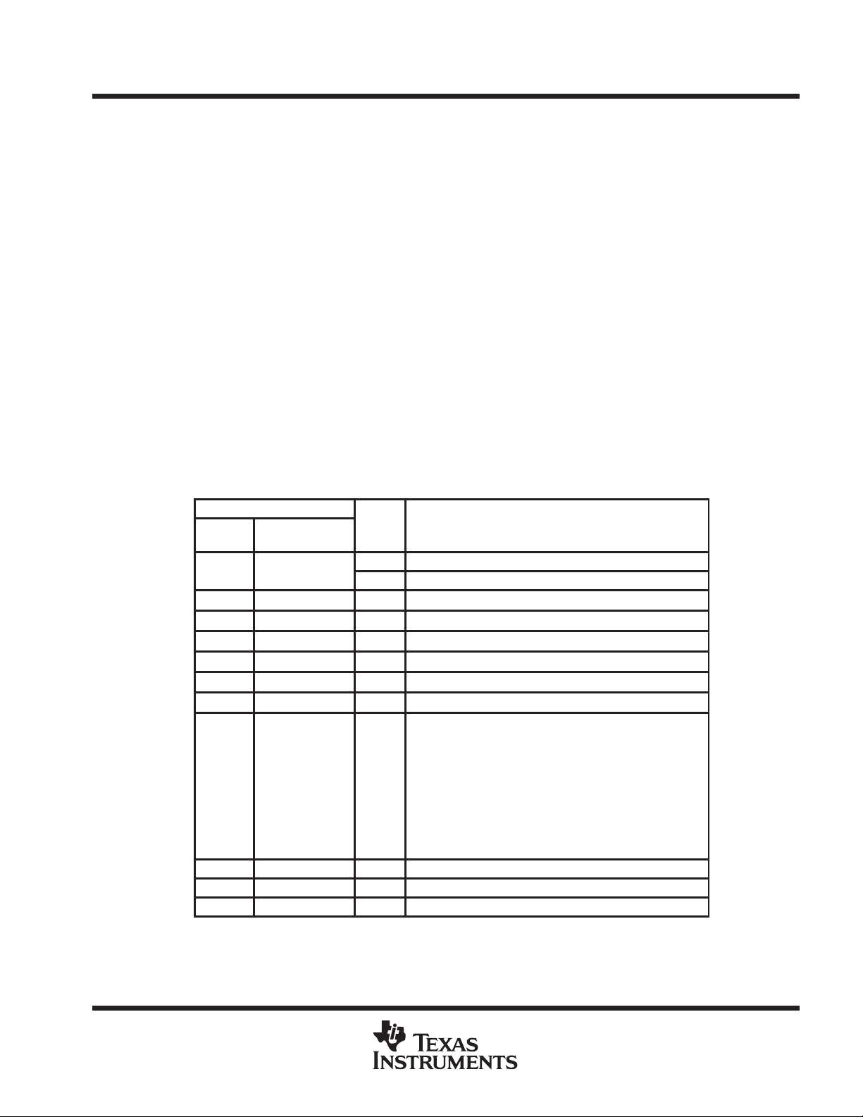
register programming
See Figure 4 for timing and format details.
Table 2. System Control Register (SCR)
REGISTER
NAME
SCR1
SCR2
SCR3
SCR4
SCR5
SCR6
SCR7
SCR8 1000 R/W Reserved
SCR9 1001 R/W D[7:0] = receive-channel offset word [7:0]
SCR10 1010 R/W D[7:0] = receive-channel offset word [15:8]
NOTES: 1. All blank bits should be filled with 0s during register write operation.
ADDRESS
S3, S2, S1, S0
0001 R/W D[4:0]= transmit-channel PAA control.
0010 R/W D[3:0] = receive-channel PGA2 control.
0011 R/W D[2:0] = receive-channel PGA1 control.
0100 Reserved
0101 Reserved
0110 R/W D[7:0] = general-purpose output control.
0111 R/W
2. All registers, except for chip ID, are set to 0 at power on.
MODE FUNCTION
R D6: chip ID = 1
W D0: software reset (self clearing). D1–D7 reserved.
Miscellaneous control (set to 1 to enable)
D0: enable TX DHPF (25.875 kHz)
D1: software power-down RX channel with reference on
D2: software power-down TX channel with reference on
D3: analog loopback. TXP and TXM are internally
connected to RXP and RXM.
D4: digital loopback. RX channel digital output is internally
connected to TX channel digital input.
D5: TX parallel interface (read-back) test mode enable
D6–D7: reserved
POST OFFICE BOX 655303 • DALLAS, TEXAS 75265
7
 Loading...