Texas Instruments TLV320AC40IPT, TLV320AC40CDW Datasheet
TLV320AC40, TLV320AC41
3-V VOICE-BAND AUDIO PROCESSORS (VBAP)
SLWS045A – JUNE 1996 – REVISED APRIL 1997
1
POST OFFICE BOX 655303 • DALLAS, TEXAS 75265
D
Single 3-V Operation
D
Low Power Consumption:
– Operating Mode ... 20 mW Typ
– Standby Mode ... 5 mW Typ
– Power-Down Mode ... 2 mW Typ
D
Combined A/D, D/A, and Filters
D
Extended Variable-Frequency Operation
– Sample Rates up to 16 kHz
– Passband up to 7.2 kHz
D
Electret Microphone Bias Reference
Voltage Available
D
Drive a Piezo Speaker Directly
D
Compatible With All Digital Signal
Processors (DSPs)
D
Selectable Between 8-Bit Companded and
13-Bit (Dynamic Range) Linear Conversion:
– TLV320AC40 . . . µ-Law and Linear
Modes
– TLV320AC41 ... A-Law and Linear
Modes
D
Programmable Volume Control in Linear
Mode
D
300-Hz to 3.6-kHz Passband with Specified
Master Clock
D
Designed for Standard 1.152-MHz Master
Clock in DECT Standard for Hand-Held
Battery-Powered T elephones
1
2
3
4
5
6
7
8
9
10
20
19
18
17
16
15
14
13
12
11
PDN
EARA
EARB
EARGS
V
CC
MICMUTE
DCLKR
DIN
FSR
EARMUTE
MICBIAS
MICGS
MICIN
VMID
GND
LINSEL
TSX/DCLKX
DOUT
FSX
CLK
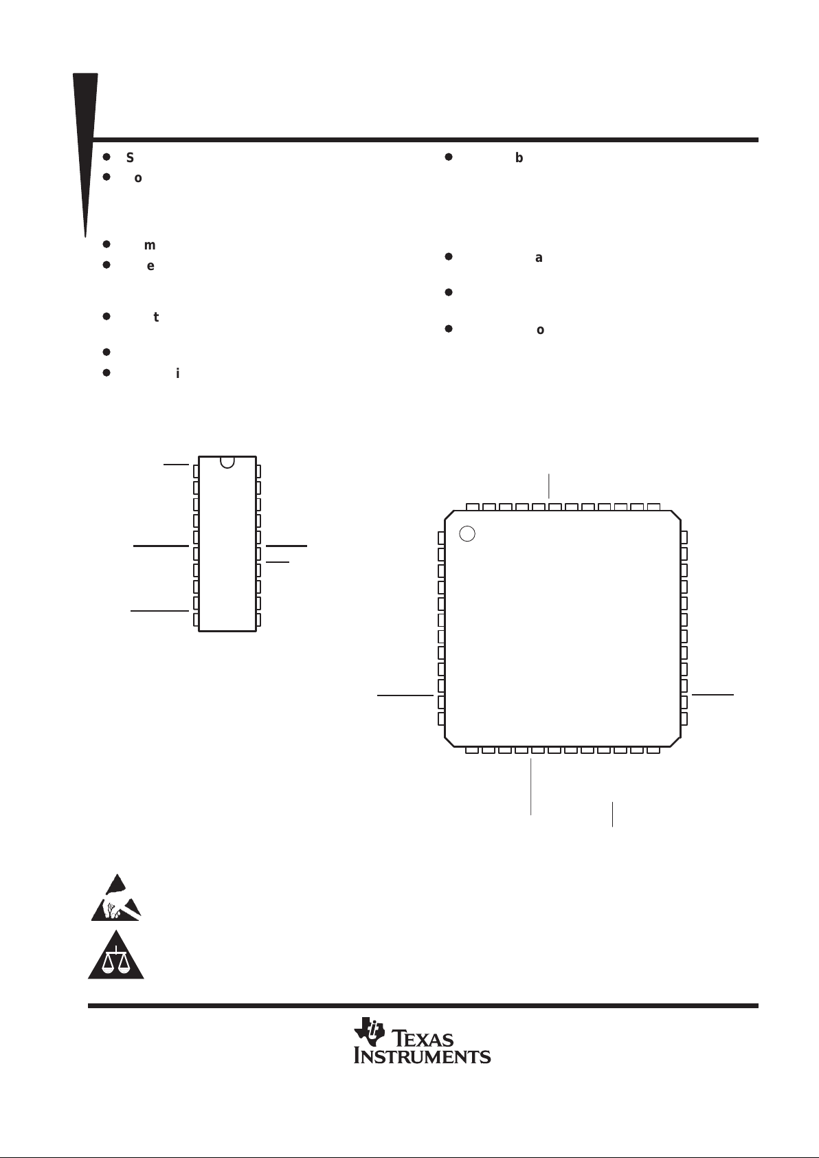
DW OR N PACKAGE
(TOP VIEW)
14 15
VMID
NC
AGND
NC
NC
NC
NC
NC
NC
DGND
LINSEL
NC
36
35
34
33
32
31
30
29
28
27
26
25
16
1
2
3
4
5
6
7
8
9
10
11
12
NC
NC
NC
AV
CC
NC
NC
NC
NC
DV
CC
NC
MICMUTE
NC
17 18 19 20
PT PACKAGE
(TOP VIEW)
MICGS
MICINNCNC
47 46 45 44 4348 42
NCNCEARGS
EARB
EARA
PDN
TSX/DCLKX
NC
NC
DIN
EARMUTE
NC
CLK
FSX
DOUT
40 39 3841
21
22 23 24
37
13
NC
MICBIAS
NC
DCLKR
FSR
NC – No internal connection
These devices have limited built-in ESD protection. The leads should be shorted together or the device placed in conductive foam
during storage or handling to prevent electrostatic damage to the MOS gates.
Please be aware that an important notice concerning availability, standard warranty, and use in critical applications of
Texas Instruments semiconductor products and disclaimers thereto appears at the end of this data sheet.
VBAP is a trademark of Texas Instruments Incorporated.
PRODUCTION DATA information is current as of publication date.
Products conform to specifications per the terms of Texas Instruments
standard warranty. Production processing does not necessarily include
testing of all parameters.
Copyright 1997, Texas Instruments Incorporated

TLV320AC40, TLV320AC41
3-V VOICE-BAND AUDIO PROCESSORS (VBAP)
SLWS045A – JUNE 1996 – REVISED APRIL 1997
2
POST OFFICE BOX 655303 • DALLAS, TEXAS 75265
description
The TLV320AC40 and TLV320AC41 voice-band audio processor (VBAP) integrated circuits perform the
transmit encoding (A/D conversion) and receive decoding (D/A conversion) together with transmit and receive
filtering for voice-band communications systems. Cellular telephone systems are targeted in particular;
however, these integrated circuits can function in other systems including digital audio, telecommunications,
and data acquisition.
These devices are pin-selectable for either of two modes — companded and linear — providing data in two
formats. In the companded mode, data is transmitted and received in 8-bit words. In the linear mode, 13 bits
of data, and either three bits of gain-setting control data, or three 0 bits of padding (to create a16-bit word), are
sent and received.
The transmit section is designed to interface directly with an electret microphone element. The microphone input
signal (MICIN) is buffered and amplified with provision for setting the amplifier gain to accommodate a range
of signal input levels. The amplified signal is passed through antialiasing and bandpass filters. The filtered signal
is then applied to the input of a compressing analog-to-digital converter (COADC) when companded mode is
selected. Otherwise, the analog-to-digital converter performs a linear conversion. The resulting data is then
clocked out of DOUT as a serial data stream.
The receive section converts a frame of serial data on DIN to analog through an expanding digital-to-analog
converter (EXDAC) when the companded mode is selected; otherwise, a linear conversion is performed. The
analog signal then passes through switched capacitor filters, which provide out-of-band rejection, (sin x)/x
correction functions, and smoothing. The filtered signal is sent to the earphone amplifier. The earphone amplifier
has a differential output with adjustable gain and is designed to minimize static power dissipation.
A single on-chip high-precision band-gap circuit generates all voltage references, eliminating the need for
external reference voltages. An internal reference voltage, VMID, equal to V
CC
/2 is used to develop the midlevel
virtual ground for all the amplifier circuits and the microphone bias circuit. Another reference voltage, MICBIAS,
can supply bias current for the microphone.
The TL V320AC4xC devices are characterized for operation from 0°C to 70°C. The TLV320AC4xI devices are
characterized for operation from –40°C to 85°C.
TLV320AC40, TLV320AC41
3-V VOICE-BAND AUDIO PROCESSORS (VBAP)
SLWS045A – JUNE 1996 – REVISED APRIL 1997
3
POST OFFICE BOX 655303 • DALLAS, TEXAS 75265
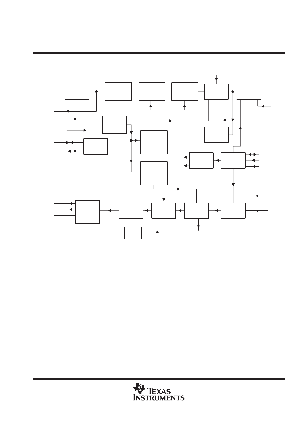
functional block diagram
12
13
8
DIN
FSR
7
14
15
LINSEL
1
PDN
16
GND
5
V
CC
10
4
3
2
EARMUTE
EARGS
EARB
EARA
Earphone
Amplifier
288 kHz
A/D
Converter
Voltage
Reference
Band-Gap
Voltage
Reference
8 kHz
288 kHz
Clock
Generator
Autozero
DCLKR
CLK
TSX
/DCLKX
FSX
DOUT
Output
Logic
ADC
MICGS
20
17
19
18
6
VMID
MICBIAS
VMID
VMID
Generator
MICIN
MICMUTE
Input
Buffer
Receive
Buffer
Receive
Filter
DAC
Input
Logic
288 kHz 8 kHz
9
15
11
Transmit
Third-Order
Antialias
Transmit
Sixth-Order
Low Pass
Transmit
First-Order
High Pass
D/A
Converter
Voltage
Reference
Clock
Control
NOTE A: Terminal numbers shown are for the DW and N packages.
LINSEL
TLV320AC40, TLV320AC41
3-V VOICE-BAND AUDIO PROCESSORS (VBAP)
SLWS045A – JUNE 1996 – REVISED APRIL 1997
4
POST OFFICE BOX 655303 • DALLAS, TEXAS 75265
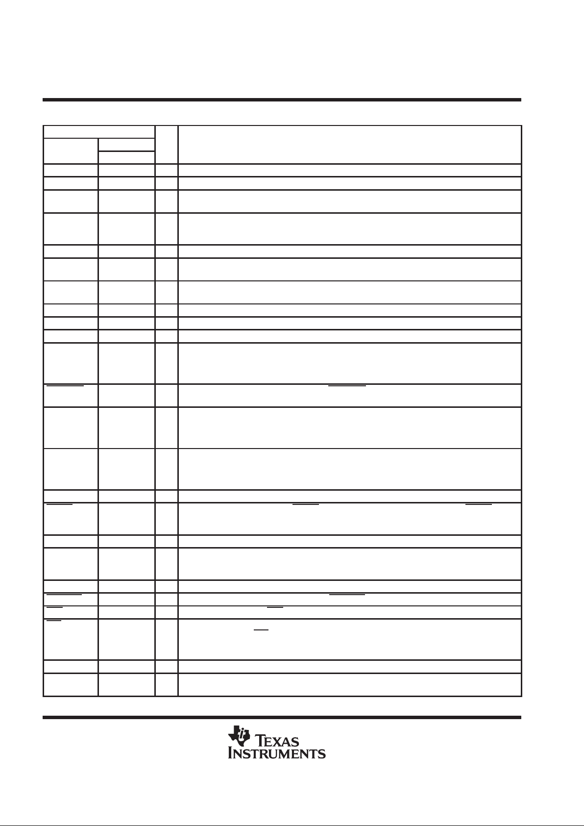
Terminal Functions
TERMINAL
NO.
I/O DESCRIPTION
NAME
DW, N PT
AGND — 34 Ground return for all internal analog circuits
AV
CC
— 4 3-V supply voltage for all internal analog circuits
CLK 11 19 I Clock input. In the fixed-data-rate mode, CLK is the master clock input as well as the transmit and
receive data clock input . In the variable-data-rate mode, CLK is the master clock input only (digital).
DCLKR 7 14 I Selection of fixed- or variable-data-rate operation. When DCLKR is connected to VCC, the device
operates in the fixed-data-rate mode. When DCLKR is not connected to VCC, the device operates in
the variable-data-rate mode and DCLKR becomes the receive data clock (digital).
DGND — 27 Ground return for all internal digital circuits
DIN 8 15 I Receive data input. Input data is clocked in on consecutive negative transitions of the receive data
clock, which is CLK for a fixed data rate and DCLKR for a variable data rate (digital).
DOUT 13 21 O Transmit data output. Transmit data is clocked out on consecutive positive transitions of the transmit
data clock, which is CLK for a fixed data rate and DCLKX for a variable data rate (digital).
DV
CC
— 9 3-V supply voltage for all internal digital circuits
EARA 2 44 O Earphone output. EARA forms a differential drive when used with the EARB signal (analog).
EARB 3 45 O Earphone output. EARB forms a differential drive when used with the EARA signal (analog).
EARGS 4 46 I Earphone gain set input of feedback signal for the earphone output. The ratio of an external potential
divider network connected across EARA and EARB adjusts the power amplifier gain. Maximum gain
occurs when EARGS is connected to EARB. Minimum gain occurs when EARGS is connected to
EARA. Earphone frequency response correction is performed using an RC approach (analog).
EARMUTE 10 17 I Earphone output mute control signal. When EARMUTE is low, the output amplifier is disabled and no
audio is sent to the earphone (digital).
FSR 9 16 I Frame-synchronization clock input for the receive channel. In the variable-data-rate mode, this signal
must remain high for the duration of the time slot. The receive channel enters the standby condition
when FSR is TTL-low for five frames or longer. The device enters a production test-mode condition
when either FSR or FSX is held high for five frames or longer (digital).
FSX 12 20 I Frame synchronization clock input for the transmit channel. FSX operates independently of FSR, but
also in an analogous manner to FSR. The transmit channel enters the standby condition when FSX is
low for five frames or longer. The device enters a production test-mode condition when either FSX or
FSR is held high for five frames or longer (digital).
GND 16 — Ground return for all internal circuits
LINSEL 15 26 I Linear selection input. When low , LINSEL selects linear coding/decoding. When high, LINSEL selects
companded coding/decoding. Companding code on the ’AC40 is µ-law , and companding code on the
’AC41 is A-law (digital).
MICBIAS 20 42 O Microphone bias. MICBIAS voltage for the electret microphone is equal to VMID.
MICGS 19 41 O Output of the internal microphone amplifier. MICGS is used as the feedback to set the microphone
amplifier gain. If sidetone is required, it is accomplished by connecting a series network between
MICGS and EARGS (analog).
MICIN 18 40 I Microphone input. Electret microphone input to the internal microphone amplifier (analog)
MICMUTE 6 11 I Microphone input mute control signal. When MICMUTE is active (low), zero code is transmitted (dig.).
PDN 1 43 I Power-down input. When PDN is low, the device powers down to reduce power consumption (digital).
TSX/DCLKX 14 22 I/O Transmit time slot strobe (active-low output) or data clock (input) for the transmit channel. In the
fixed-data-rate mode, TSX
/DCLKX is an open-drain output that pulls to ground and is used as an enable
signal for a 3-state buffer. In the variable-data-rate mode, DCLKX becomes the transmit data clock input
(digital).
V
CC
5 — 3-V supply voltage for all internal circuits
VMID 17 36 O VCC/2 bias voltage reference. A pair of external, low-leakage, high-frequency capacitors
(1 µF and 470 pF) should be connected between VMID and ground for filtering.
TLV320AC40, TLV320AC41
3-V VOICE-BAND AUDIO PROCESSORS (VBAP)
SLWS045A – JUNE 1996 – REVISED APRIL 1997
5
POST OFFICE BOX 655303 • DALLAS, TEXAS 75265
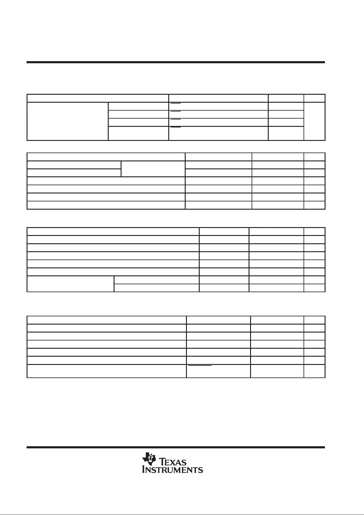
absolute maximum ratings over operating free-air temperature range (unless otherwise noted)
†
Supply voltage range, V
CC
(see Note 1) –0.3 V to 5.5 V. . . . . . . . . . . . . . . . . . . . . . . . . . . . . . . . . . . . . . . . . . . . .
Output voltage range at DOUT, VO –0.3 V to 5.5 V. . . . . . . . . . . . . . . . . . . . . . . . . . . . . . . . . . . . . . . . . . . . . . . . . .
Input voltage range at DIN, V
I
–0.3 V to 5.5 V. . . . . . . . . . . . . . . . . . . . . . . . . . . . . . . . . . . . . . . . . . . . . . . . . . . . . .
Continuous total power dissipation See Dissipation Rating Table. . . . . . . . . . . . . . . . . . . . . . . . . . . . . . . . . . . . .
Operating free-air temperature range: C suffix 0°C to 70°C. . . . . . . . . . . . . . . . . . . . . . . . . . . . . . . . . . . . . . . . . .
I suffix –40°C to 85°C. . . . . . . . . . . . . . . . . . . . . . . . . . . . . . . . . . . . . . . . .
Storage temperature range, T
stg
–65°C to 150°C. . . . . . . . . . . . . . . . . . . . . . . . . . . . . . . . . . . . . . . . . . . . . . . . . . .
Lead temperature 1,6 mm (1/16 inch) from case for 10 seconds 260°C. . . . . . . . . . . . . . . . . . . . . . . . . . . . . . .
†
Stresses beyond those listed under “absolute maximum ratings” may cause permanent damage to the device. These are stress ratings only, and
functional operation of the device at these or any other conditions beyond those indicated under “recommended operating conditions” is not
implied. Exposure to absolute-maximum-rated conditions for extended periods may affect device reliability.
NOTE 1: Voltage value is with respect to GND.
DISSIPATION RATING TABLE
PACKAGE
TA ≤ 25°C
POWER RATING
DERATING FACTOR
ABOVE TA = 25°C
TA = 70°C
POWER RATING
TA = 85°C
POWER RATING
DW 1025 mW 8.2 mW/°C 656 mW 533 mW
N 1150 mW 9.2 mW/°C 736 mW 598 mW
PT 1075 mW 7.1 mW/°C 756 mW 649 mW
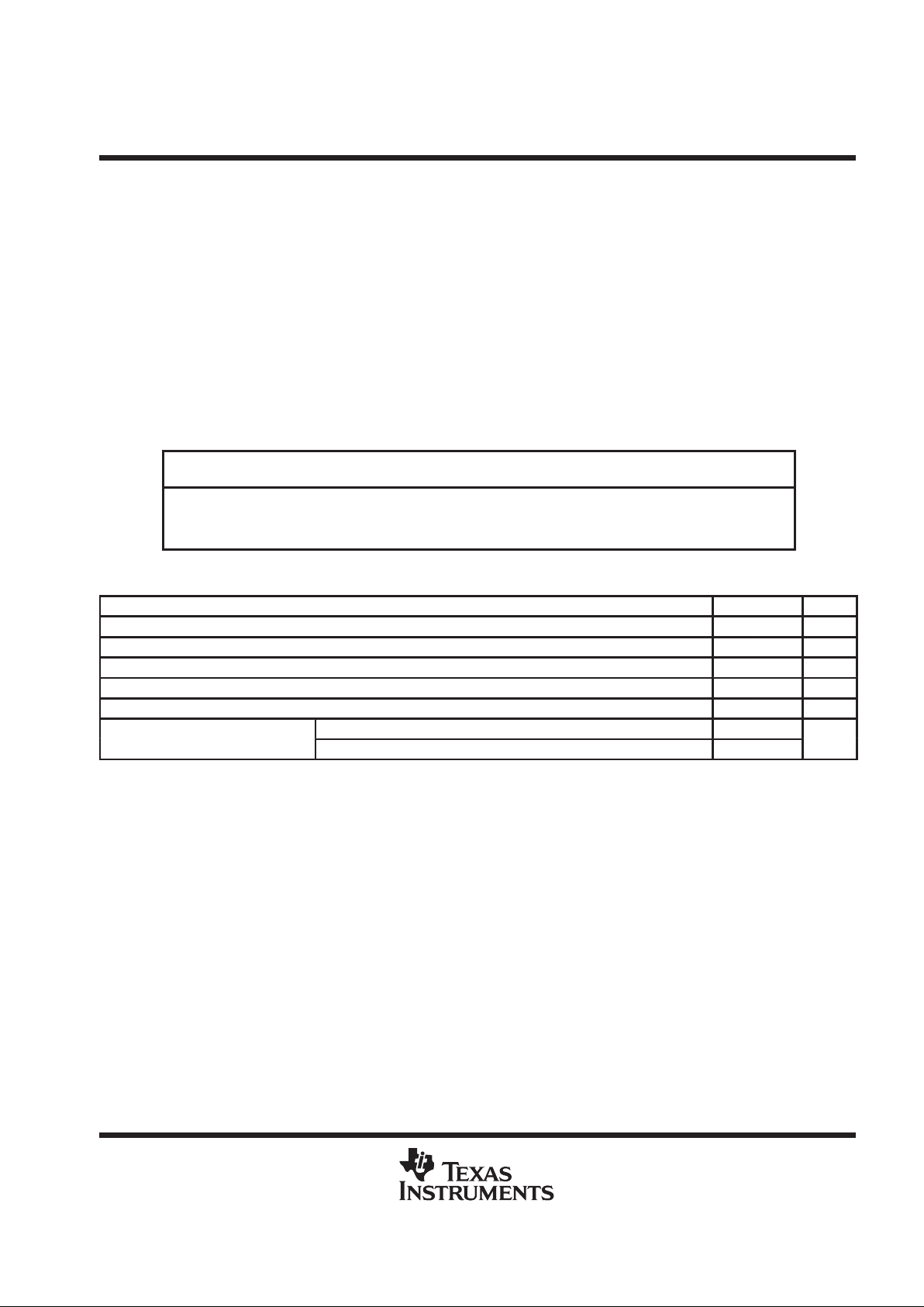
recommended operating conditions (see Note 2)
MIN MAX UNIT
Supply voltage, VCC (see Note 3) 2.7 3.3 V
High-level input voltage, V
IH
2.2 V
Low-level input voltage, V
IL
0.8 V
Load resistance between EARA and EARB, RL (see Note 4) 600 Ω
Load capacitance between EARA and EARB, CL (see Note 4) 50 nF
p
p
TLV320AC40C, TLV320AC41C 0 70
°
Operating free-air temperature, T
A
TLV320AC40I, TLV320AC41I –40 85
°C
NOTES: 2. To avoid possible damage to these CMOS devices and resulting reliability problems, the power-up sequence detailed in the system
reliability features paragraph should be followed.
3. Voltages at analog inputs, outputs, and VCC are with respect to GND.
4. RL and CL should not be applied simultaneously.
TLV320AC40, TLV320AC41
3-V VOICE-BAND AUDIO PROCESSORS (VBAP)
SLWS045A – JUNE 1996 – REVISED APRIL 1997
6
POST OFFICE BOX 655303 • DALLAS, TEXAS 75265
electrical characteristics over recommended ranges of supply voltage and free-air temperature
(unless otherwise noted)
supply current, f
DCLKR
or f
DCLKX
= 1.152 MHz, outputs not loaded, VCC = 3 V, TA = 25°C
PARAMETER TEST CONDITIONS MIN MAX UNIT
Operating PDN is high with CLK signal present 7.5
Power down PDN is low for 500 µs 0.75
I
CC
Supply current from V
CC Standby – both PDN is high with FSX and FSR held low 2
mA
Standby – one
PDN is high with either FSX or FSR pulsing
with the other held low
4.5
digital interface
PARAMETER TEST CONDITIONS MIN TYP†MAX UNIT
V
OH
High-level output voltage
IOH = –3.2 mA, VCC = 3 V 2.4 2.8 V
V
OL
Low-level output voltage
DOUT
IOL = 3.2 mA, VCC = 3 V 0.2 0.4 V
I
IH
High-level input current, any digital input VI = 2.2 V to V
CC
10 µA
I
IL
Low-level input current, any digital input VI = 0 to 0.8 V 10 µA
C
i
Input capacitance 5 pF
C
o
Output capacitance 5 pF
†
All typical values are at VCC = 3 V, TA = 25°C.
microphone interface
PARAMETER TEST CONDITIONS MIN TYP†MAX UNIT
V
IO
Input offset voltage at MICIN VI = 0 to 3 V ±5 mV
I
IB
Input bias current at MICIN ±200 nA
B
1
Unity-gain bandwidth, open loop at MICIN
‡
1.5 MHz
C
i
Input capacitance at MICIN 5 pF
A
V
Large-signal voltage amplification at MICGS 10000 V/V
p
VMID 3 µA
IOmaxMaximum output current
MICBIAS (source only) 1 mA
†
All typical values are at VCC = 3 V, TA = 25°C.
‡
The frequency of the first pole is 100 Hz.
speaker interface
PARAMETER TEST CONDITIONS MIN TYP†MAX UNIT
V
O(PP)
AC output voltage 3§Vpp
V
OO
Output offset voltage at EARA, EARB (single-ended) Relative to GND 80 mVpk
I
I(lkg)
Input leakage current at EARGS VI = 0.5 V to (VCC – 0.5) V ±200 nA
IOmax Maximum output current RL = 600 Ω ±2.5 mA
r
o
Output resistance at EARA, EARB 1 Ω
Gain change
EARMUTE low, max level
when muted
–60 dB
†
All typical values are at VCC = 3 V, TA = 25°C.
§
2.5 Vpp when VCC is 2.7 V.
TLV320AC40, TLV320AC41
3-V VOICE-BAND AUDIO PROCESSORS (VBAP)
SLWS045A – JUNE 1996 – REVISED APRIL 1997
7
POST OFFICE BOX 655303 • DALLAS, TEXAS 75265
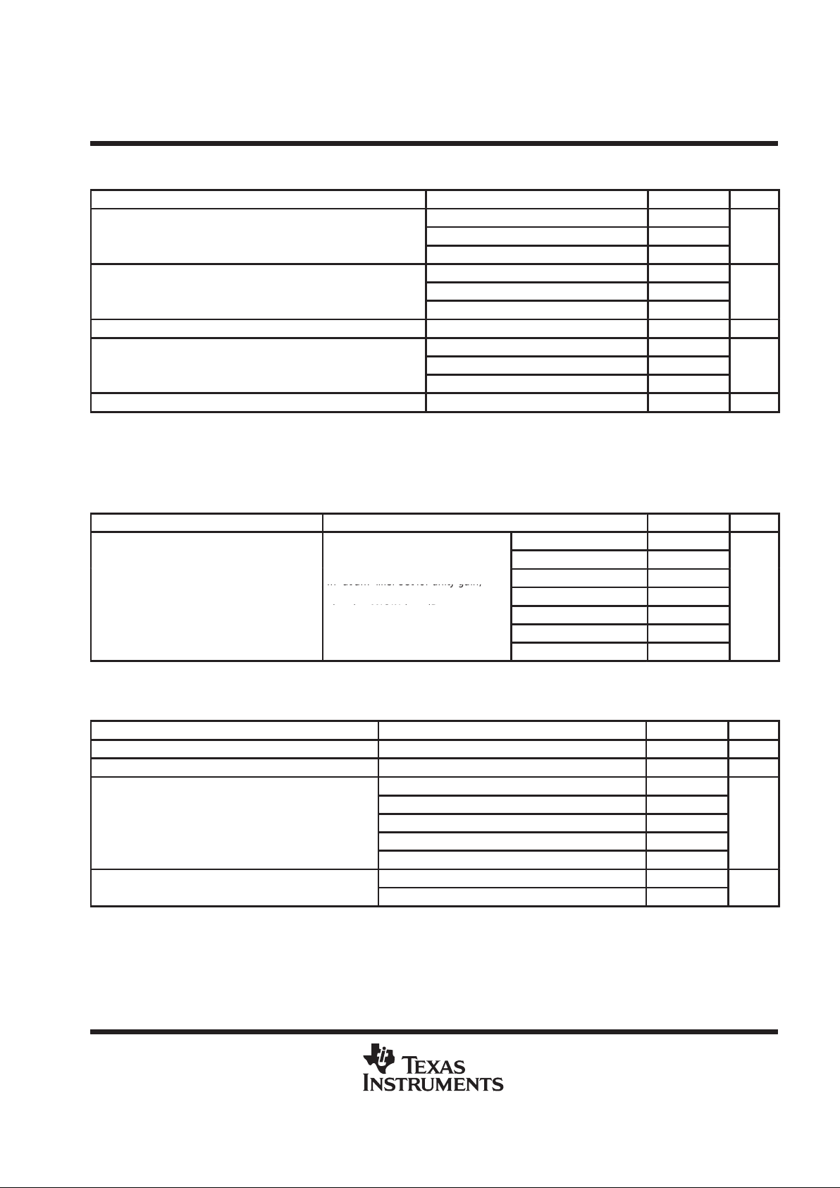
transmit gain and dynamic range, companded mode (µ-law or A-law) or linear mode selected, VCC = 3 V,
TA = 25°C (unless otherwise noted) (see Notes 5 and 6)
PARAMETER TEST CONDITIONS MIN MAX UNIT
Companded mode selected, µ-law (’AC40) 0.614
Transmit reference-signal level (0 dB) (see Note 7)
Companded mode selected, A-law (’AC41) 0.616
Vrms
Linear mode selected (’AC40 and ’AC41) 0.626
Companded mode selected, µ-law (’AC40) 2.5
Overload-signal level (MICIN at unity gain)
Companded mode selected, A-law (’AC41) 2.5
Vpp
Linear mode selected (’AC40 and ’AC41) 2.5
Absolute gain error 0-dB input signal ±1 dB
MICIN to DOUT at 3 dBm0 to –40 dBm0 ±0.5
Gain error with input level relative to gain at –10 dBm0
MICIN to DOUT at –41 dBm0 to –50 dBm0 ±1.5
dB
MICIN to DOUT at –51 dBm0 to –55 dBm0 ±2
Gain variation VCC ±10%, TA = 0°C to 70°C ±0.5 dB
NOTES: 5. Unless otherwise noted, the analog input is 0 dB, 1020-Hz sine wave, where 0 dB is defined as the zero-reference point of the channel
under test.
6. The input amplifier is set for inverting unity gain.
7. The reference-signal level, which is input to the transmit channel, is defined as a value 3 dB below the full-scale value of 2 V.
transmit filter transfer, companded mode (µ-law or A-law) or linear mode selected, over recommended
ranges of supply voltage and free-air temperature, CLK = 1.152 MHz, FSX = 8 kHz (see Note 6)
PARAMETER TEST CONDITIONS MIN MAX UNIT
f
MICIN
= 50 Hz –10 0
f
MICIN
= 200 Hz –2.8 0
Input amplifier set for unity gain
,
f
MICIN
= 300 Hz to 3 kHz ±0.25
Gain relative to input signal gain at 1.02 kHz
In ut am lifier set for unity gain,
noninverting maximum gain output
f
MICIN
= 3.3 kHz –0.55 0.2
dB
signal at MICIN is 0 dB
f
MICIN
= 3.4 kHz –1 –0.1
f
MICIN
= 4 kHz –14
f
MICIN
≥4.6 kHz –32
NOTE 6. The input amplifier is set for inverting unity gain.
transmit idle channel noise and distortion, companded mode with µ-law or A-law selected, over
recommended ranges of supply voltage and operating free-air temperature (see Note 8)
PARAMETER TEST CONDITIONS MIN MAX UNIT
Transmit noise, psophometrically weighted MICIN connected to MICGS through a 10-kΩ resistor –72 dBm0p
Transmit noise, C-message weighted MICIN connected to MICGS through a 10-kΩ resistor 10 dBrnC0
MICIN to DOUT at 0 dBm0 to –24 dBm0 36
MICIN to DOUT at –25 dBm0 to –30 dBm0 34
Transmit signal-to-distortion ratio with sine-wave input
MICIN to DOUT at –31 dBm0 to –38 dBm0 30
dB
MICIN to DOUT at –39 dBm0 to –40 dBm0 24
MICIN to DOUT at –41 dBm0 to –45 dBm0 20
Intermodulation distortion, 2-tone CCITT method,
CCITT G.712 (7.1), R2 49
composite power level –13 dBm0
CCITT G.712 (7.2), R3 51
dB
NOTE 8: Transmit noise, linear mode: 200 µVrms is equivalent to –74 dB (referenced to device 0-dB level).
 Loading...