

DEVICE
SHUTDOWN
Selecti
(
OU060)
(Lit # SLOU060)
TLV2780, TLV2781, TLV2782, TLV2783, TLV2784, TLV2785, TLV278xA
FAMILY OF 1.8 V HIGH-SPEED RAIL-TO-RAIL INPUT/OUTPUT
OPERATIONAL AMPLIFIERS WITH SHUTDOWN
SLOS245 – MARCH 2000
D
Supply Voltage Range . . . 1.8 V to 3.6 V
D
Rail-to-Rail Input/Output
D
High Bandwidth ...8 MHz
D
High Slew Rate . . . 4.8 V/µs
D
V
Exceeds Rails . . . –0.2 V to VDD+ 0.2
ICR
D
Supply Current . . . 650 µA/Channel
D
Input Noise Voltage ...9 nV/√Hz at 10 kHz
D
Specified Temperature Range
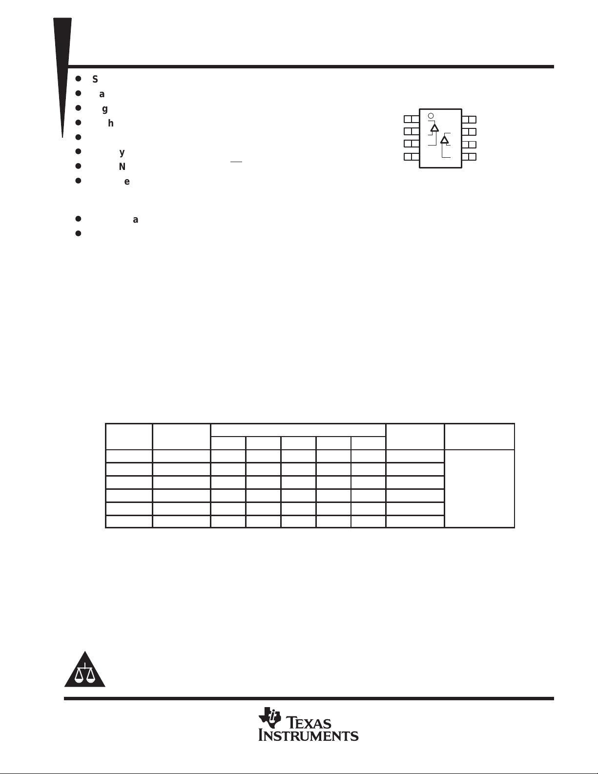
D, DGK, OR P PACKAGE
1OUT
1IN–
1IN+
GND
TLV2782
(TOP VIEW)
1
2
3
4
8
7
6
5
V
DD
2OUT
2IN–
2IN+
– 0°C to 70°C... Commercial Grade
– –40°C to 125°C... Industrial Grade
D
Ultra-Small Packaging
D
Universal Op Amp EVM
description
The TL V278x single supply operational amplifiers provide rail-to-rail input and output capability. The TLV278x
takes the minimum operating supply voltage down to 1.8 V over the extended industrial temperature range
(–40°C to 125°C) while adding the rail-to-rail output swing feature. The TL V278x also provides 8 MHz bandwidth
from only 650 µA of supply current. The maximum recommended supply voltage is 3.6 V, which allows the
devices to be operated from (±1.8 V supplies down to ±0.9 V) two rechargable cells.
The combination of wide bandwidth, low noise, and low distortion makes it ideal for high speed and high
resolution data converter applications. Its high output drive and bandwidth means that it is also suitable for video
line driving applications.
All members are available in PDIP , SOIC, and the newer , smaller SOT -23 (singles), MSOP (duals), and TSSOP
(quads).
FAMILY PACKAGE TABLE
NO. OF
CHANNELS
TLV2780
TLV2781
TLV2782 2 8 8 — — 8 —
TLV2783 2 14 14 — — 10 Yes
TLV2784
TLV2785
†
†
†
†
†
This device is in the Product Preview stage of development. Contact the local TI sales office for more
information.
1 8 8 6 — — Yes
1 8 8 5 — — —
4 14 14 — 14 — —
4 16 16 — 16 — Yes
PDIP SOIC SOT-23 TSSOP MSOP
PACKAGE TYPES
UNIVERSAL
EVM BOARD
Refer to the EVM
on Guide
Lit # SL
Please be aware that an important notice concerning availability, standard warranty, and use in critical applications of
Texas Instruments semiconductor products and disclaimers thereto appears at the end of this data sheet.
This document contains information on products in more than one phase
of development. The status of each device is indicated on the page(s)
specifying its electrical characteristics.
POST OFFICE BOX 655303 • DALLAS, TEXAS 75265
Copyright 2000, Texas Instruments Incorporated
1
TLV2780, TLV2781, TLV2782, TLV2783, TLV2784, TLV2785, TLV278xA
AT 25 C
3000 µV
AT 25 C
OUTLINE
†
DIP
DIP
40°C to 125°C
V
40°C to 125°C
FAMILY OF 1.8 V HIGH-SPEED RAIL-TO-RAIL INPUT/OUTPUT
OPERATIONAL AMPLIFIERS WITH SHUTDOWN
SLOS245 – MARCH 2000
TLV2780 and TLV2781 AVAILABLE OPTIONS
T
A
0°C to 70°C
-40°C to 125°C
†
This package is available taped and reeled. To order this packaging option, add an R suffix to the part number (e.g., TLV2780CDR).
‡
This package is only available taped and reeled. For standard quantities (3,000 pieces per reel), add a R suffix (i.e., TL V2780CDBVR). For smaller
quantities (250 pieces per mini-reel), add a T suffix to the part number (e.g. TLV2780CDBVT).
T
A
0°C to 70°C 3000 µV
°
–
†
This package is available taped and reeled. To order this packaging option, add an R suffix to the part number (e.g., TLV2782CDR).
VIOmax
3000 µV
°
2000 µV
VIOmax
°
°
SMALL
(D)
TLV2782CD
TLV2783CD
TLV2782ID
TLV2783ID
TLV2782AID
TLV2783AID
SMALL OUTLINE
TLV2782 and TLV2783 AVAILABLE OPTIONS
†
(D)
TLV2780CD
TLV2781CD
TLV2780ID
TLV2781ID
†
(DGK)
TLV2782CDGK—xxTIAAI
TLV2782IDGK—xxTIAAJ
—
—
SYMBOL (DGS)
PACKAGED DEVICES
SOT-23
(DBV)‡ SYMBOL
TLV2780CDBV
TLV2781CDBV
TLV2780IDBV
TLV2781IDBV
PACKAGED DEVICES
MSOP
—
—
—
—
—
TLV2783CDGS—xxTIAAK
—
TLV2783IDGS—xxTIAAL—TLV2783IN
—
—
PLASTIC DIP
(P)
VAOC
VAPC
VAOI
VAPI
PLASTIC
†
SYMBOL
—
—
TLV2780IP
TLV2781IP
(N)
—
—
—
—
—
—
PLASTIC
(P)
—
—
TLV2782IP
—
—
—
TLV2784 and TLV2785 AVAILABLE OPTIONS
max
T
A
0°C to 70°C 3000 µV
°
–
†
This package is available taped and reeled. T o order this packaging option, add an R suffix to the part number
(e.g., TLV2784CDR).
°
IO
AT 25°C
3000 µV
2000 µV
SMALL OUTLINE
(D)
TLV2784CD
TLV2785CD
TLV2784ID
TLV2785ID
TLV2784AID
TLV2785AID
PACKAGED DEVICES
PLASTIC DIP
(N)
—
—
TLV2784IN
TLV2785IN
—
—
†
TSSOP
(PW)
TLV2784CPW
TLV2785CPW
TLV2784IPW
TLV2785IPW
TLV2784AIPW
TLV2785AIPW
2
POST OFFICE BOX 655303 • DALLAS, TEXAS 75265
TLV2780, TLV2781, TLV2782, TLV2783, TLV2784, TLV2785, TLV278xA
FAMILY OF 1.8 V HIGH-SPEED RAIL-TO-RAIL INPUT/OUTPUT
OPERATIONAL AMPLIFIERS WITH SHUTDOWN
SLOS245 – MARCH 2000
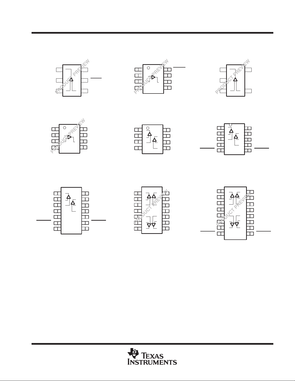
TLV278x PACKAGE PINOUTS
OUT
GND
IN+
D OR P PACKAGE
NC
IN–
IN+
GND
D OR N PACKAGE
TLV2780
DBV PACKAGE
(TOP VIEW)
1
6
2
5
3
4
TLV2781
(TOP VIEW)
1
2
3
4
(TOP VIEW)
8
7
6
5
TLV2783
V
DD
SHDN
IN–
NC
V
DD
OUT
NC
TLV2780
D OR P PACKAGE
(TOP VIEW)
NC
IN–
IN+
GND
D, DGK, OR P PACKAGE
1OUT
1IN–
1IN+
GND
1
2
3
4
TLV2782
(TOP VIEW)
1
2
3
4
TLV2784
D, N, OR PW PACKAGE
(TOP VIEW)
TLV2781
DBV PACKAGE
(TOP VIEW)
SHDN
8
V
7
6
5
8
7
6
5
DD
OUT
NC
V
DD
2OUT
2IN–
2IN+
OUT
GND
IN+
1OUT
1IN–
1IN+
GND
1SHDN
1
2
3
TLV2783
DGS PACKAGE
(TOP VIEW)
1
10
2
3
4
5
TLV2785
D, N, OR PW PACKAGE
(TOP VIEW)
V
5
4
9
8
7
6
DD
IN–
V
DD
2OUT
2IN–
2IN+
2SHDN
1OUT
1IN–
1IN+
GND
NC
1SHDN
NC
NC – No internal connection
1
14
2
13
3
12
4
11
5
10
6
7
1
V
DD
2OUT
2IN–
2IN+
NC
2SHDN
9
8
NC
1OUT
1IN–
1IN+
V
DD
2IN+
2IN–
2OUT
14
4OUT
2
13
4IN–
3
12
4IN+
4
11
GND
5
10
3IN+
6
7
9
3IN–
8
3OUT
1OUT
1IN–
1IN+
V
DD
2IN+
2IN–
2OUT
1SHDN
1
16
2
15
3
14
4
13
5
12
6
11
7
10
8
4OUT
4IN–
4IN+
GND
3IN+
3IN–
3OUT
9
2SHDN
POST OFFICE BOX 655303 • DALLAS, TEXAS 75265
3
TLV2780, TLV2781, TLV2782, TLV2783, TLV2784, TLV2785, TLV278xA
PACKAGE
JC
JA
A
Suppl
oltage, V
V
Operating free-air temperature, T
°C
‡
V
FAMILY OF 1.8 V HIGH-SPEED RAIL-TO-RAIL INPUT/OUTPUT
OPERATIONAL AMPLIFIERS WITH SHUTDOWN
SLOS245 – MARCH 2000
absolute maximum ratings over operating free-air temperature range (unless otherwise noted)
Supply voltage, VDD (see Note 1) 4 V. . . . . . . . . . . . . . . . . . . . . . . . . . . . . . . . . . . . . . . . . . . . . . . . . . . . . . . . . . . . .
Differential input voltage, VID ±V
Input current, I
(any input) ± 10 mA. . . . . . . . . . . . . . . . . . . . . . . . . . . . . . . . . . . . . . . . . . . . . . . . . . . . . . . . . . . . . .
I
Output current, IO ± 10 mA. . . . . . . . . . . . . . . . . . . . . . . . . . . . . . . . . . . . . . . . . . . . . . . . . . . . . . . . . . . . . . . . . . . . . .
Continuous total power dissipation See Dissipation Rating Table. . . . . . . . . . . . . . . . . . . . . . . . . . . . . . . . . . . . .
Operating free-air temperature range, TA: C suffix 0°C to 70°C. . . . . . . . . . . . . . . . . . . . . . . . . . . . . . . . . . . . . .
Maximum junction temperature, T
Storage temperature range, T
Lead temperature 1,6 mm (1/16 inch) from case for 10 seconds 260°C. . . . . . . . . . . . . . . . . . . . . . . . . . . . . . .
†
Stresses beyond those listed under “absolute maximum ratings” may cause permanent damage to the device. These are stress ratings only, and
functional operation of the device at these or any other conditions beyond those indicated under “recommended operating conditions” is not
implied. Exposure to absolute-maximum-rated conditions for extended periods may affect device reliability.
NOTE 1: All voltage values, except differential voltages, are with respect to GND.
D (8) 38.3 176 710 mW
D (14) 26.9 122.3 1022 mW
D (16) 25.7 114.7 1090 mW
DBV (5) 55 324.1 385 mW
DBV (6) 55 294.3 425 mW
DGK (8) 54.23 259.96 481 mW
DGS (10) 54.1 257.71 485 mW
N (14, 16) 32 78 1600 mW
P (8) 41 104 1200 mW
PW (14) 29.3 173.6 720 mW
PW (16) 28.7 161.4 774 mW
. . . . . . . . . . . . . . . . . . . . . . . . . . . . . . . . . . . . . . . . . . . . . . . . . . . . . . . . . . . . . . .
I suffix –40°C to 125°C. . . . . . . . . . . . . . . . . . . . . . . . . . . . . . . . . . . .
150°C. . . . . . . . . . . . . . . . . . . . . . . . . . . . . . . . . . . . . . . . . . . . . . . . . . . . . . . . .
J
–65°C to 150°C. . . . . . . . . . . . . . . . . . . . . . . . . . . . . . . . . . . . . . . . . . . . . . . . . . .
stg
DISSIPATION RATING TABLE
Θ
(°C/W)
Θ
(°C/W)
T
≤ 25°C
POWER RATING
†
DD
recommended operating conditions
pp
y v
Common-mode input voltage range, V
p
Shutdown on/off voltage level
‡
Relative to GND.
4
DD
MIN MAX UNIT
Single supply 1.8 3.6
Split supply ±0.9 ±1.8
ICR
p
A
C-suffix 0 70
I-suffix –40 125
VDD < 2.7 V 0.75V
IH
VDD = 2.7 to 3.6 V 2
V
IL
POST OFFICE BOX 655303 • DALLAS, TEXAS 75265
–0.2 VDD+0.2 V
°
DD
V
0.6
,
TLV278
VIOInput offset voltage
V
IC
VDD/2,
V
TLV278xA
8µV/°C
V
1.8 V
IC DD
CMRR
Common-mode rejection ratio
V
2.7 V/ 3.6 V
dB
IC DD
V
2.7 V/ 3.6 V
V
V
A
gg g
L
,
V/mV
V
2.7 V/ 3.6 V
V
Common-mode input voltage range
CMRR
V
V
IC
VDD/2
ODD
TLV2780, TLV2781, TLV2782, TLV2783, TLV2784, TLV2785, TLV278xA
FAMILY OF 1.8 V HIGH-SPEED RAIL-TO-RAIL INPUT/OUTPUT
OPERATIONAL AMPLIFIERS WITH SHUTDOWN
SLOS245 – MARCH 2000
electrical characteristics at specified free-air temperature, VDD = 1.8 V, 2.7 V (unless otherwise
noted)
dc performance
PARAMETER TEST CONDITIONS
DD
DD
DD
DD
DD
x
=
=
=
= 1.8
=
V
= V
/2
p
α
†
Temperature coefficient of input offset
VIO
voltage
Large-signal differential voltage R
VD
amplification
Full range is 0°C to 70°C for the C suffix and –40°C to 125°C for the I suffix. If not specified, full range is –40°C to 125°C.
VO = VDD/2,
RL = 2 kΩ,
RS = 50 Ω
VIC = 0 to VDD,
RS = 50 Ω
VIC = 1.2 V to VDD,
RS = 50 Ω
= 2 kΩ,
V
= 1 V
O(PP)
†
T
A
25°C 250 3000
Full range 4500
25°C 250 2000
Full range 3000
25°C 50 76
Full range 50
25°C 55 80
Full range 50
25°C 70 100
Full range 70
25°C 200 600
Full range 50
25°C 200 1000
Full range 70
MIN TYP MAX
UNIT
µ
°
input characteristics
PARAMETER TEST CONDITIONS
ICR
I
I
r
C
†
Input offset current
IO
Input bias current
IB
Differential input resistance 25°C 1000 GΩ
i(d)
Common-mode input capacitance f = 1 kHz 25°C 2.8 pF
i(c)
Full range is 0°C to 70°C for the C suffix and –40°C to 125°C for the I suffix. If not specified, full range is –40°C to 125°C.
p
Measured over
range,
RS = 50 Ω
=
=
VO = VDD/2,
RL = 2 kΩ,
RS = 50 Ω
,
VDD = 1.8 V
VDD = 2.7 V
TLV278xC Full range 100
TLV278xI Full range 300
TLV278xC Full range 100
TLV278xI Full range 300
†
T
A
25°C or
full range
25°C or-
Full range
25°C 2.5 15
25°C 2.5 15
MIN TYP MAX
–0.2
to
2
–0.2
to
2.9
UNIT
pA
pA
POST OFFICE BOX 655303 • DALLAS, TEXAS 75265
5
TLV2780, TLV2781, TLV2782, TLV2783, TLV2784, TLV2785, TLV278xA
V
V
I
OH
mA
V
2.7 V
VOHHigh-level output voltage
V
V
V
I
OH
mA
V
V
IC DD
,
VOLLow-level output voltage
V
V
mV
IC DD
,
V
V
DD
,
IOOutput current
25°C17mA
DD
,
Sourcing
IOSShort-circuit output current
25°C21mA
Sinking
IDDSupply current (per channel)
V
VDD/2
SHDN
V
A
DD
,
,
k
ygj
DD
,
,
dB
DD
,
,
FAMILY OF 1.8 V HIGH-SPEED RAIL-TO-RAIL INPUT/OUTPUT
OPERATIONAL AMPLIFIERS WITH SHUTDOWN
SLOS245 – MARCH 2000
electrical characteristics at specified free-air temperature, VDD = 1.8 V, 2.7 V (unless otherwise
noted) (continued)
output characteristics
PARAMETER TEST CONDITIONS
= 1.8
DD
VIC = VDD/2,
= –1
–
p
VIC = VDD/2,
= –5
–
V
= V
= V
= 1.8 V,
= 2.7 V,
/2,
/2,
IOL = 1 mA
p
p
p
†
Full range is 0°C to 70°C for the C suffix and –40°C to 125°C for the I suffix. If not specified, full range is –40°C to 125°C.
V
IOL = 5 mA
V
VO = 0.5 V from
V
VO = 0.5 V from
=
DD
VDD = 3.6 V 25°C 3.58
= 1.8
DD
= 2.7
DD
VDD = 3.6 V 25°C 3.55
= 1.8
DD
= 2.7
DD
Positive rail 10
Negative rail
Positive rail
Negative rail 23
VDD = 1.8 V 13
VDD = 2.7 V
VDD = 1.8 V
VDD = 2.7 V 45
†
T
A
25°C 1.7 1.77
Full range 1.63
25°C 2.6 2.68
Full range 2.6
25°C 1.5 1.55
Full range 1.46
25°C 2.5 2.55
Full range 2.45
25°C 70
Full range 80
25°C 180 240
Full range 290
25°C 120 170
Full range 200
°
°
MIN TYP MAX
15
35
UNIT
power supply
pp
Supply voltage rejection ratio V
SVR
(∆VDD /∆VIO)
†
Full range is 0°C to 70°C for the C suffix and –40°C to 125°C for the I suffix. If not specified, full range is –40°C to 125°C.
6
PARAMETER TEST CONDITIONS
p
=
O
V
VIC = VDD/2
VIC = VDD/2
V
VIC = VDD/2
POST OFFICE BOX 655303 • DALLAS, TEXAS 75265
,
= 1.8 V to 2.7 V, No load,
= 2.7 V to 3.6 V, No load,
= 1.8 V to 3.6 V, No load,
=
DD
Full range
Full range 58
Full range 70
Full range 60
†
T
A
25°C 650 770
25°C 60 75
25°C 75 90
25°C 65 80
MIN TYP MAX
820
UNIT
µ
V
V
SR+Positive slew rate at unity gain
R
C
V
2.7 V
C
L
F
V
V
V/µs
V
V
SR–Negative slew rate at unity gain
R
V
2.7 V
C
L
F
V
V
R
2 kΩ
C
25 pF
25°C
(STEP)PP
,
tsSettling time
25°C
s
(STEP)PP
,
V
O(PP)
VDD/2
25°C
VnEquivalent input noise voltage
V/√H
I
y,
SHDN
V
nA
25°C
ns
TLV2780, TLV2781, TLV2782, TLV2783, TLV2784, TLV2785, TLV278xA
FAMILY OF 1.8 V HIGH-SPEED RAIL-TO-RAIL INPUT/OUTPUT
OPERATIONAL AMPLIFIERS WITH SHUTDOWN
SLOS245 – MARCH 2000
electrical characteristics at specified free-air temperature, VDD = 1.8 V, 2.7 V (unless otherwise
noted) (continued)
dynamic performance
PARAMETER TEST CONDITIONS
UGBW Unity gain bandwidth
φ
m
†
Full range is 0°C to 70°C for the C suffix and –40°C to 125°C for the I suffix. If not specified, full range is –40°C to 125°C.
Phase margin
Gain margin
RL = 2 kΩ,C
V
= 1 V,
O(PP)
= 2 kΩ,
L
= 50 pF
= 50
V
= 1 V,
O(PP)
= 2 kΩ,
L
= 50 pF
C
= 50
,
=
L
VDD = 1.8 V,
V
AV = –1,
CL = 10 pF, RL = 2 kΩ
VDD = 2.7 V,
V
AV = –1,
CL = 10 pF, RL = 2 kΩ
= 1 V,
= 1 V,
= 25 pF
L
= 1.8
DD
=
DD
= 3.6
DD
= 1.8
DD
=
DD
= 3.6
DD
p
=
L
0.1% 1.7
0.01%
0.1%
0.01% 2.4
†
T
A
25°C 8 MHz
25°C
Full range 3.1
25°C
Full range 3.5
25°C
Full range 3.6
25°C
Full range 1.89
25°C
Full range 1.97
25°C
Full range 3.4
°
°
MIN TYP MAX UNIT
3.3 4.3
3.8 4.8
4 5
2.1 2.8
2.2 2.8
3.5 4.2
58°
8 dB
2.8
1.7
µ
noise/distortion performance
PARAMETER TEST CONDITIONS
THD + N Total harmonic distortion plus noise
p
I
n
Equivalent input noise current f = 1 kHz 0.9
T
A
=
=
RL = 2 kΩ,
f = 10 kHz
f = 1 kHz
f = 10 kHz 9
,
AV = 1 0.055%
AV = 10 0.08%
AV = 100
MIN TYP MAX
0.45%
18
UNIT
n
fA/√Hz
shutdown characteristics
PARAMETER TEST CONDITIONS
DD(SHDN)
t
(on)
t
(off)
†
Full range is 0°C to 70°C for the C suffix and –40°C to 125°C for the I suffix. If not specified, full range is –40°C to 125°C.
‡
Disable time and enable time are defined as the interval between application of the logic signal to SHDN and the point at which the supply current
has reached half its final value.
Supply current, all channels in shutdown mode
(TLV2780, TLV2783, TLV2785)
Amplifier turnon time
Amplifier turnoff time
‡
‡
= 0
RL = 2 kΩ
RL = 2 kΩ
†
T
A
25°C 900 1400
Full range 1700
°
MIN TYP MAX
800
200
UNIT
z
POST OFFICE BOX 655303 • DALLAS, TEXAS 75265
7
TLV2780, TLV2781, TLV2782, TLV2783, TLV2784, TLV2785, TLV278xA
SR
Slew rate
FAMILY OF 1.8 V HIGH-SPEED RAIL-TO-RAIL INPUT/OUTPUT
OPERATIONAL AMPLIFIERS WITH SHUTDOWN
SLOS245 – MARCH 2000
TYPICAL CHARACTERISTICS
Table of Graphs
FIGURE
V
IO
CMRR Common-mode rejection ratio vs Frequency 3
V
OH
V
OL
V
O(PP)
Z
o
I
DD
I
DD
PSRR Power supply rejection ratio vs Frequency 12
A
VD
φ
m
V
n
I
DD(SHDN)
I
DD(SHDN)
I
DD(SHDN)
Input offset voltage vs Common-mode input voltage 1, 2
High-level output voltage vs High-level output current 4, 6
Low-level output voltage vs Low-level output current 5, 7
Maximum peak-to-peak output voltage vs Frequency 8
Output impedance vs Frequency 9
Supply current vs Supply voltage 10
Supply current vs Free-air temperature 11
Differential voltage amplification & phase vs Frequency 13
Gain-bandwidth product vs Free-air temperature 14
vs Supply voltage 15
vs Free-air temperature 16, 17
Phase margin vs Load capacitance 18
Equivalent input noise voltage vs Frequency 19
Voltage-follower large-signal pulse response vs Time 20
Voltage-follower small-signal pulse response vs Time 21
Inverting large-signal pulse response vs Time 22
Inverting small-signal pulse response vs Time 23
Crosstalk vs Frequency 24
Shutdown forward & reverse isolation vs Frequency 25
Shutdown supply current vs Free-air temperature 26
Shutdown supply current vs Supply voltage 27
Shutdown supply current/output voltage vs Time 28
8
POST OFFICE BOX 655303 • DALLAS, TEXAS 75265

TLV2780, TLV2781, TLV2782, TLV2783, TLV2784, TLV2785, TLV278xA
FAMILY OF 1.8 V HIGH-SPEED RAIL-TO-RAIL INPUT/OUTPUT
OPERATIONAL AMPLIFIERS WITH SHUTDOWN
SLOS245 – MARCH 2000
TYPICAL CHARACTERISTICS
INPUT OFFSET VOLTAGE
vs
COMMON-MODE INPUT VOLTAGE
400
VDD=1.8 V
200
TA=25° C
0
–200
–400
–600
Input Offset Voltage ––Vµ
–800
IO
V
–1000
–0.2 0 0.2 0.4 0.6 0.8 1 1.2 1.4 1.6 1.8 2
V
– Common-Mode Input Voltage – V
ICR
Figure 1
HIGH-LEVEL OUTPUT VOLTAGE
vs
HIGH-LEVEL OUTPUT CURRENT
1.8
1.6
1.4
1.2
1.0
0.8
0.6
0.4
– High-Level Output Voltage – V
0.2
OH
V
0.0
TA=125°C
TA=70°C
TA=25°C
TA=0°C
TA=40°C
0246810121416
IOH – High-Level Output Current – mA
VDD=1.8 V
INPUT OFFSET VOLTAGE
vs
COMMON-MODE INPUT VOLTAGE
100
VDD=2.7 V
50
TA=25 °C
0
–50
–100
–150
–200
–250
Input Offset Voltage ––Vµ
–300
IO
V
–350
–400
–0.2 0.2 0.6 1 1.4 1.8 2.2 2.6 3
V
– Common-Mode Input Voltage – V
ICR
Figure 2
LOW-LEVEL OUTPUT VOLTAGE
vs
LOW-LEVEL OUTPUT CURRENT
1.8
VDD=1.8 V
1.6
1.4
1.2
1.0
0.8
0.6
0.4
0.2
OL
V – Low-Level Output Voltage – V
0.0
TA=125°C
TA=70°C
TA=25°C
TA=0°C
TA=–40°C
0 2 4 6 8 10 12 1416 18 20 22 24 28
IOL – Low-Level Output Current – mA
COMMON-MODE REJECTION RATIO
vs
140
130
120
110
100
90
80
70
60
50
40
30
20
10
0
CMRR – Common-Mode Rejection Ratio – dB
FREQUENCY
VDD = 3.6 V
VDD = 2.7 V
VDD = 1.8 V
0 10 100 10k 1M 10M
1k 100k
f – Frequency – Hz
Figure 3
HIGH-LEVEL OUTPUT VOLTAGE
vs
HIGH-LEVEL OUTPUT CURRENT
2.7
2.4
2.1
1.8
1.5
TA=125°C
TA=70°C
1.2
0.9
0.6
– High-Level Output Voltage – V
0.3
OH
V
26
TA=25°C
TA=0°C
TA=–40°C
0
0 5 10 15 20 25 30 35 40
IOH – High-Level Output Current – mA
VDD = 2.7 V
Figure 4
LOW-LEVEL OUTPUT VOLTAGE
vs
LOW-LEVEL OUTPUT CURRENT
2.7
VDD= 2.7 V
2.4
2.1
1.8
1.5
1.2
0.9
0.6
OL
0.3
V – Low-Level Output Voltage – V
0.0
TA=125°C
TA= 70°C
TA=25°C
TA=0°C
TA=–40°C
0 5 10 15 20 25 30 35 40 45 50 55
IOL – Low-Level Output Current – mA
Figure 7
Figure 5
MAXIMUM PEAK-TO-PEAK
OUTPUT VOLTAGE
vs
V
O(PP)
AV = –10
RL=2 kΩ
CL = 10 pF
TA = 25° C
FREQUENCY
V
= 2.7 V
O(PP)
= 1.8 V
f – Frequency – Hz
2.8
2.6
2.4
2.2
2.0
1.8
1.6
1.4
1.2
1.0
0.8
– Maximum Peak-To-Peak Output Voltage – V
0.6
0.4
100 1 k 10 k 100 k 1 M 10 M
O(PP)
V
Figure 8
POST OFFICE BOX 655303 • DALLAS, TEXAS 75265
Figure 6
OUTPUT IMPEDANCE
vs
FREQUENCY
100
VDD = 2.7 V
TA = 25° C
Ω
10
AV = 10
1
– Output Impedance –Z
o
AV = 1
0.1
100 1k 10k 100k 1M 10M
f – Frequency – Hz
Figure 9
9

TLV2780, TLV2781, TLV2782, TLV2783, TLV2784, TLV2785, TLV278xA
FAMILY OF 1.8 V HIGH-SPEED RAIL-TO-RAIL INPUT/OUTPUT
OPERATIONAL AMPLIFIERS WITH SHUTDOWN
SLOS245 – MARCH 2000
TYPICAL CHARACTERISTICS
SUPPLY CURRENT
vs
700
600
500
400
300
200
DD
I Supply Current – –Aµ
100
SUPPLY VOLTAGE
TA = 125°C
TA = –40°C
TA = 25°C
AV= 1
VIC = V
0
0 0.6 1.2 1.8 2.4 3 3.6
VDD – Supply Voltage – V
DD/2
V
1.4
1.35
1.3
1.25
1.2
1.15
– Supply Current – mA
1.1
DD
I
1.05
1
–40 –25 –10 5 20 35 50 65 80 95 110 125
Figure 10
DIFFERENTIAL VOLTAGE AMPLIFICATION AND PHASE
vs
80
70
60
50
40
Phase
30
20
10
0
–10
–20
– Differential Voltage Amplification – dBA
–30
VD
–40
1 k 10 k 100 k
FREQUENCY
VDD = 1.8 V & 2.7 V
RL= 2 kΩ
CL = 10 pF
TA = 25° C
Gain
f – Frequency – Hz
1 M 10 M
Figure 13
SUPPLY CURRENT
vs
FREE-AIR TEMPERATURE
VDD = 3.6 V
VDD = 2.7 V
VDD = 1.8 V
AV = 1
VIC = VDD/2
TA – Free-Air Temperature – °C
Figure 11
240
210
180
150
120
90
60
30
Phase Margin – °
0
–30
–60
–90
–120
POWER SUPPLY REJECTION RATIO
vs
FREQUENCY
120
100
80
60
40
– Power Supply Rejection Ratio – dBPSRR
20
0
10 100 1 k 10 k 100 k 1 M 10 M
f – Frequency – Hz
Figure 12
GAIN-BANDWIDTH PRODUCT
vs
FREE-AIR TEMPERATURE
9
8
7
6
5
4
3
2
RL = 2 kΩ
Gain-Bandwidth Product – MHz
CL = 10 pF
1
f = 10 kHz
0
–40 –25 –10 5 20 35 50 65 80 95 110 125
TA – Free-Air Temperature – °C
VDD = 1.8 V
VDD = 2.7 V
Figure 14
VDD=2.7 V
TA=25°C
SLEW RATE
vs
SUPPLY VOLTAGE
8
7
6
5
4
3
SR – Slew Rate – V/µs
2
1
0
1.8 2 2.2 2.4 2.6 2.8 3 3.2 3.4 3.6
SR–
SR+
VDD – Supply Voltage – V
Figure 15
10
AV = 1
RL = 2 kΩ
CL =10 pF
VO = 1 V
PP
VIC = VDD/2
TA = 25° C
SLEW RATE
vs
FREE-AIR TEMPERATURE
6
5
4
3
2
SR – Slew Rate – V/µs
1
0
–40 –25 –10 5 20 35 50 65 80 95 110 125
SR+
SR–
VDD = 1.8 V
AV = 1
RL=2 kΩ
CL=10 pF
VIC = VDD/2
TA – Free-Air Temperature – °C
Figure 16
POST OFFICE BOX 655303 • DALLAS, TEXAS 75265
SLEW RATE
vs
FREE-AIR TEMPERATURE
6
5
4
3
2
SR – Slew Rate – V/µs
1
0
–40–25 –10 5 20 35 50 65 80 95 110 125
SR+
SR–
VDD = 2.7 V
AV = 1
RL= 2 kΩ
CL = 10 pF
VO = 1 V
VIC = VDD/2
TA – Free-Air Temperature – °C
Figure 17
PP

TLV2780, TLV2781, TLV2782, TLV2783, TLV2784, TLV2785, TLV278xA
FAMILY OF 1.8 V HIGH-SPEED RAIL-TO-RAIL INPUT/OUTPUT
OPERATIONAL AMPLIFIERS WITH SHUTDOWN
SLOS245 – MARCH 2000
TYPICAL CHARACTERISTICS
PHASE MARGIN
vs
100
– Phase Margin – °
m
φ
LOAD CAPACITANCE
90
80
70
60
50
40
30
VDD = 2.7 V
20
RL = 2 kΩ
AV = 1
10
TA = 25°C
0
10 100 1 k 10 k
CL – Load Capacitance – pF
Rnull=50 Ω
Rnull=20 Ω
Rnull=0 Ω
Figure 18
VOLTAGE-FOLLOWER LARGE-SIGNAL PULSE RESPONSE
vs
TIME
V
I
2.5
2
1.5
1
– Output Voltage – VV
0.5
O
0
VDD = 2.7 V
V
O
RL = 2 kΩ
CL = 10 pF
AV = 1
TA = 25°C
0 0.2 0.4 0.6 0.8 1 1.2 1.4 1.6 1.8
t – Time – µs
2.5
2
1.5
1
0.5
– Input Voltage – VV
I
Figure 20
EQUIVALENT INPUT NOISE VOLTAGE
vs
140
120
nV/ Hz– Equivalent Input Noise Voltage –V
100
80
60
40
20
0
10 100 1 k 10 k 100 k
n
FREQUENCY
TA = 25°C
VDD = 2.7 V
VDD = 1.8 V
f – Frequency – Hz
Figure 19
VOLTAGE-FOLLOWER SMALL-SIGNAL PULSE RESPONSE
vs
– Output Voltage – VV
TIME
V
I
V
1.40
1.35
1.30
O
1.25
O
VDD = 2.7 V
RL = 2 kΩ
CL = 10 pF
AV = 1
TA = 25°C
0 0.2 0.4 0.6 0.8 1 1.2 1.4
t – Time – µs
1.45
1.40
1.35
1.30
1.25
– Input Voltage – VV
I
Figure 21
INVERTING LARGE-SIGNAL PULSE RESPONSE
vs
TIME
V
I
2.5
2
1.5
1
V
0.5
– Output Voltage – VV
O
0
VDD = 2.7 V
RL = 2 kΩ
CL = 10 pF
AV = –1
TA = 25°C
O
0 0.3 0.6 0.9 1.2 1.5 1.8 2.1 2.4 2.7 3 3.3
t – Time – µs
1
0.5
0
–0.5
–1
– Input Voltage – VV
Figure 22
POST OFFICE BOX 655303 • DALLAS, TEXAS 75265
INVERTING SMALL-SIGNAL PULSE RESPONSE
vs
TIME
V
I
V
O
VDD = 2.7 V
RL = 2 kΩ
CL = 10 pF
AV = –1
TA = 25°C
t – Time – µs
I
1.40
1.35
1.30
– Output Voltage – VV
O
1.25
0 0.3 0.6 0.9 1.2 1.5 1.8 2.1 2.4 2.7 3
0.10
0.05
0
–0.05
– Input Voltage – VV
I
Figure 23
11

TLV2780, TLV2781, TLV2782, TLV2783, TLV2784, TLV2785, TLV278xA
FAMILY OF 1.8 V HIGH-SPEED RAIL-TO-RAIL INPUT/OUTPUT
OPERATIONAL AMPLIFIERS WITH SHUTDOWN
SLOS245 – MARCH 2000
TYPICAL CHARACTERISTICS
CROSSTALK
vs
0
–20
–40
–60
–80
Crosstalk – dB
–100
–120
–140
10 100 1 k 10 k 100 k
FREQUENCY
Crosstalk in Shutdown
VDD = 1.8 V & 2.7 V
VIC = 60% of V
AV = 1
RL= 2 kΩ
TA = 25°C
All Channels
Crosstalk/No Shutdown
f – Frequency – Hz
DD
Figure 24
SHUTDOWN SUPPLY CURRENT
vs
2.6
2.4
2.2
Aµ
2
1.8
1.6
1.4
1.2
1
0.8
– Supply Current –
0.6
DD
I
0.4
0.2
0
SUPPLY VOLTAGE
Shutdown = 0 V
VIC = VDD/2
AV = 1
TA = 125°C
TA = –40°C
0 0.4 0.8 1.2 1.6 2 2.4 2.8 3.2 3.6
VDD – Supply Voltage – V
Figure 27
TA = 25°C
SHUTDOWN FORWARD +
REVERSE ISOLATION
vs
140
120
100
80
60
40
20
Shutdown Forward Isolation - dB
0
10 100 1 k 10 k 100 k 1 M 10 M
FREQUENCY
Forward and Reverse Isolation
VDD = 1.8 & 2.7 V
VIC = VDD /2
RL = 2 kΩ
CL= 10 pF
AV = 1
TA = 25°C
f – Frequency – Hz
Figure 25
SHUTDOWN SUPPLY CURRENT / OUTPUT VOLTAGE
3.0
2.5
2.0
1.5
1.0
0.5
0.0
SD – Shutdown Pulse – V
–1.5
1.5
1.3
1.0
0.8
0.5
0.3
0.0
– Output Voltage – mVV
–0.3
O
–0.5
–0.8
1.8
1.5
1.3
1.0
0.8
0.5
0.3
0.0
– Shutdown Current – mA
–0.3
–0.5
–1 0 1 2 3 4 5
DD(SD)
I
I
DD(SD)
SD
SHUTDOWN SUPPLY CURRENT
vs
FREE-AIR TEMPERATURE
3
Shutdown = 0V
VIC = VDD/2
2.5
AV = 1
2.0
1.5
VDD= 3.6 V
1
VDD = 2.7 V
0.5
DD
I Shutdown Supply Current ––Aµ
0
–40–25 –10 5 20 35 50 65 80 95 110 125
VDD = 1.8 V
TA – Free-Air Temperature – °C
Figure 26
vs
TIME
V
O
VDD = 2.7 V
AV = 1
RL = 10 kΩ
CL = 10 pF
VIC = VDD/2
TA = 25° C
t – Time – µ
67 8 10
sec
9
Figure 28
12
POST OFFICE BOX 655303 • DALLAS, TEXAS 75265
TLV2780, TLV2781, TLV2782, TLV2783, TLV2784, TLV2785, TLV278xA
FAMILY OF 1.8 V HIGH-SPEED RAIL-TO-RAIL INPUT/OUTPUT
OPERATIONAL AMPLIFIERS WITH SHUTDOWN
SLOS245 – MARCH 2000
PARAMETER MEASUREMENT INFORMATION
_
+
R
null
R
L
C
L
Figure 29
APPLICATION INFORMATION
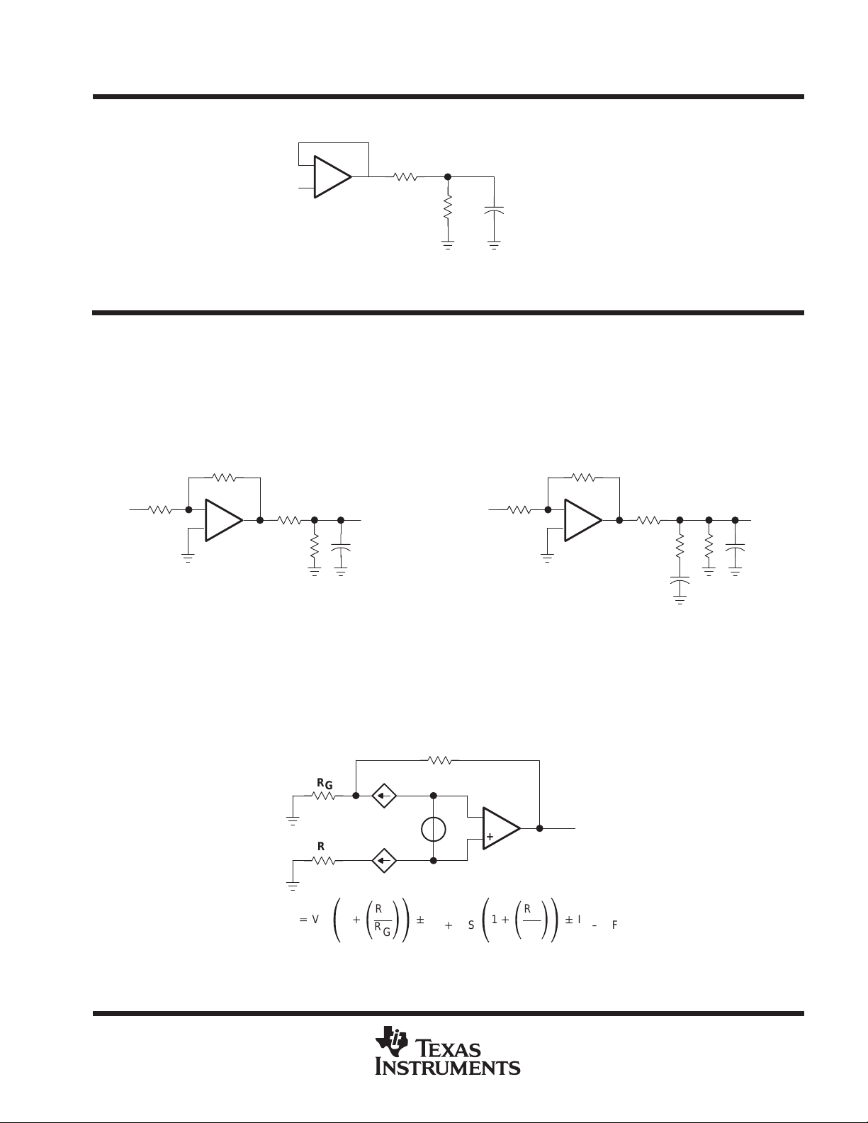
driving a capacitive load
When the amplifier is configured in this manner, capacitive loading directly on the output will decrease the
device’s phase margin leading to high frequency ringing or oscillations. Therefore, for capacitive loads of greater
than 10 pF, it is recommended that a resistor be placed in series (R
shown in Figure 30.
R
F
R
Input
G
–
+
R
NULL
Output
R
L
C
LOAD
Input
R
G
) with the output of the amplifier, as
NULL
R
F
R
–
+
NULL
Snubber
R
L
Output
C
L
C
(a) (b)
Figure 30. Driving a Capacitive Load
offset voltage
The output offset voltage, (VOO) is the sum of the input offset voltage (VIO) and both input bias currents (IIB) times
the corresponding gains. The following schematic and formula can be used to calculate the output offset
voltage:
R
F
I
VOO+
R
G
R
S
V
ǒ
IO
Figure 31. Output Offset Voltage Model
1
) ǒ
IB–
+
V
I
I
IB+
R
F
Ǔ
"
I
Ǔ
R
G
IB
)
–
+
R
1
) ǒ
F
Ǔ
R
G
R
ǒ
S
V
O
"
I
Ǔ
IB–RF
POST OFFICE BOX 655303 • DALLAS, TEXAS 75265
13
TLV2780, TLV2781, TLV2782, TLV2783, TLV2784, TLV2785, TLV278xA
FAMILY OF 1.8 V HIGH-SPEED RAIL-TO-RAIL INPUT/OUTPUT
OPERATIONAL AMPLIFIERS WITH SHUTDOWN
SLOS245 – MARCH 2000
APPLICATION INFORMATION
general configurations
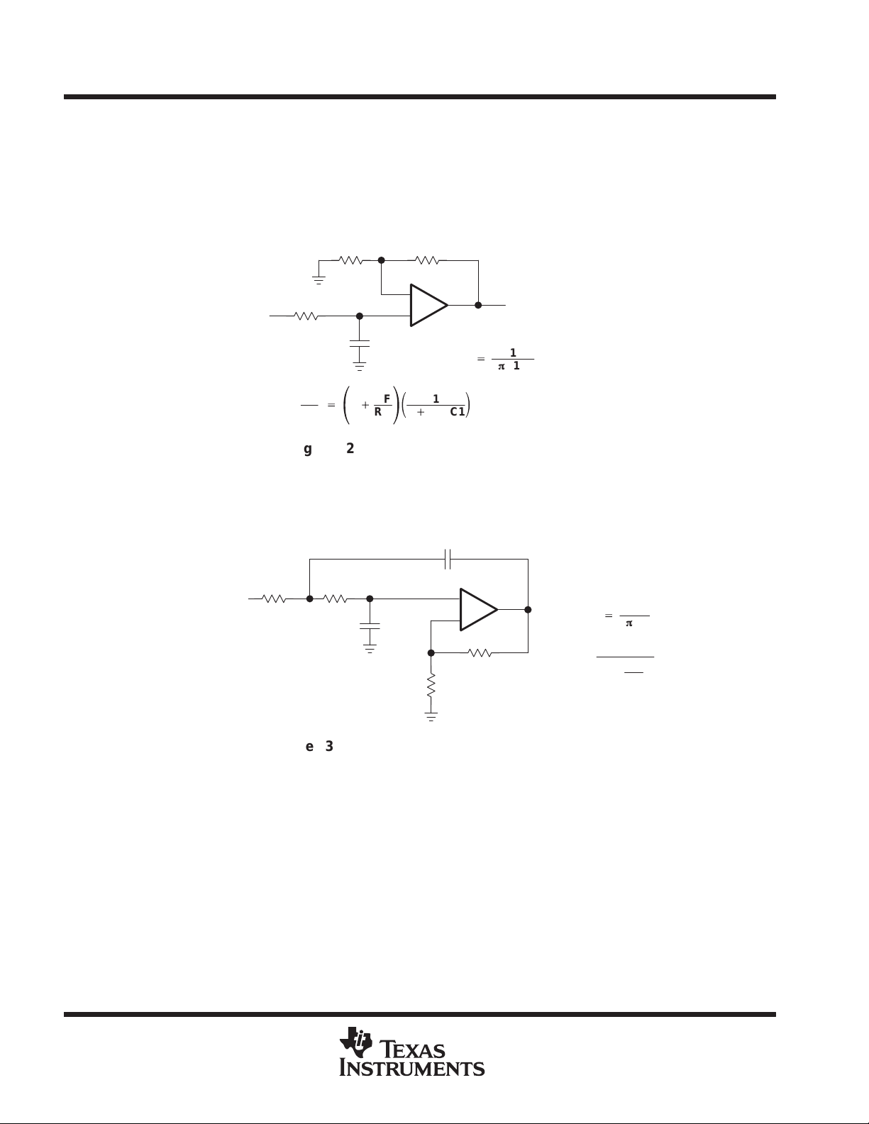
When receiving low-level signals, limiting the bandwidth of the incoming signals into the system is often
required. The simplest way to accomplish this is to place an RC filter at the noninverting terminal of the amplifer
(see Figure 32).
R
G
R
F
–
C1
R
F
R
G
+
ǒ
Ǔ
1)sR1C1
f
1
–3dB
Ǔ
V
I
R1
V
O
+ ǒ
1
V
I
)
+
V
O
1
2pR1C1
Figure 32. Single-Pole Low-Pass Filter
If even more attenuation is needed, a multiple pole filter is required. The Sallen-Key filter can be used for this
task. For best results, the amplifier should have a bandwidth that is 8 to 10 times the filter frequency bandwidth.
Failure to do this can result in phase shift of the amplifier.
C1
V
I
R2R1
C2
R
G
+
_
R
F
R1 = R2 = R
C1 = C2 = C
Q = Peaking Factor
(Butterworth Q = 0.707)
1
+
2pRC
R
F
1
2 –
(
)
Q
R
f
–3dB
G
=
14
Figure 33. 2-Pole Low-Pass Sallen-Key Filter
POST OFFICE BOX 655303 • DALLAS, TEXAS 75265

TLV2780, TLV2781, TLV2782, TLV2783, TLV2784, TLV2785, TLV278xA
FAMILY OF 1.8 V HIGH-SPEED RAIL-TO-RAIL INPUT/OUTPUT
OPERATIONAL AMPLIFIERS WITH SHUTDOWN
SLOS245 – MARCH 2000
APPLICATION INFORMATION
circuit layout considerations
T o achieve the levels of high performance of the TL V278x, follow proper printed-circuit board design techniques.
A general set of guidelines is given in the following.
D
Ground planes – It is highly recommended that a ground plane be used on the board to provide all
components with a low inductive ground connection. However, in the areas of the amplifier inputs and
output, the ground plane can be removed to minimize the stray capacitance.
D
Proper power supply decoupling – Use a 6.8-µF tantalum capacitor in parallel with a 0.1-µF ceramic
capacitor on each supply terminal. It may be possible to share the tantalum among several amplifiers
depending on the application, but a 0.1-µF ceramic capacitor should always be used on the supply terminal
of every amplifier. In addition, the 0.1-µF capacitor should be placed as close as possible to the supply
terminal. As this distance increases, the inductance in the connecting trace makes the capacitor less
effective. The designer should strive for distances of less than 0.1 inches between the device power
terminals and the ceramic capacitors.
D
Sockets – Sockets can be used but are not recommended. The additional lead inductance in the socket pins
will often lead to stability problems. Surface-mount packages soldered directly to the printed-circuit board
is the best implementation.
D
Short trace runs/compact part placements – Optimum high performance is achieved when stray series
inductance has been minimized. To realize this, the circuit layout should be made as compact as possible,
thereby minimizing the length of all trace runs. Particular attention should be paid to the inverting input of
the amplifier. Its length should be kept as short as possible. This will help to minimize stray capacitance at
the input of the amplifier.
D
Surface-mount passive components – Using surface-mount passive components is recommended for high
performance amplifier circuits for several reasons. First, because of the extremely low lead inductance of
surface-mount components, the problem with stray series inductance is greatly reduced. Second, the small
size of surface-mount components naturally leads to a more compact layout thereby minimizing both stray
inductance and capacitance. If leaded components are used, it is recommended that the lead lengths be
kept as short as possible.
POST OFFICE BOX 655303 • DALLAS, TEXAS 75265
15

TLV2780, TLV2781, TLV2782, TLV2783, TLV2784, TLV2785, TLV278xA
FAMILY OF 1.8 V HIGH-SPEED RAIL-TO-RAIL INPUT/OUTPUT
OPERATIONAL AMPLIFIERS WITH SHUTDOWN
SLOS245 – MARCH 2000
APPLICATION INFORMATION
shutdown function
Three members of the TLV278x family (TLV2780/3/5) have a shutdown terminal for conserving battery life in
portable applications. When the shutdown terminal is tied low, the supply current is reduced to 900 nA/channel,
the amplifier is disabled, and the outputs are placed in a high impedance mode. To enable the amplifier, the
shutdown terminal can either be left floating or pulled high. When the shutdown terminal is left floating, care
should be taken to ensure that parasitic leakage current at the shutdown terminal does not inadvertently place
the operational amplifier into shutdown.
general power dissipation considerations
For a given θJA, the maximum power dissipation is shown in Figure 34 and is calculated by the following formula:
T
MAX–TA
Where:
ǒ
q
= Maximum power dissipation of TLV278x IC (watts)
= Absolute maximum junction temperature (150°C)
= Free-ambient air temperature (°C)
= θ
+ θ
JC
P
T
T
θ
JA
D
MAX
A
PD+
θJC= Thermal coefficient from junction to case
θCA= Thermal coefficient from case to ambient air (°C/W)
Ǔ
JA
CA
MAXIMUM POWER DISSIPATION
vs
FREE-AIR TEMPERATURE
2
PDIP Package
1.75
1.5
SOIC Package
1.25
Low-K Test PCB
θJA = 176°C/W
1
0.75
0.5
Maximum Power Dissipation – W
SOT-23 Package
0.25
Low-K Test PCB
θJA = 324°C/W
0
–55–40 –25 –10 5
NOTE A: Results are with no air flow and using JEDEC Standard Low-K test PCB.
Low-K Test PCB
θJA = 104°C/W
20 35 50
TA – Free-Air Temperature – °C
TJ = 150°C
MSOP Package
Low-K Test PCB
θJA = 260°C/W
65 80 95 110 125
Figure 34. Maximum Power Dissipation vs Free-Air Temperature
16
POST OFFICE BOX 655303 • DALLAS, TEXAS 75265

macromodel information
TLV2780, TLV2781, TLV2782, TLV2783, TLV2784, TLV2785, TLV278xA
FAMILY OF 1.8 V HIGH-SPEED RAIL-TO-RAIL INPUT/OUTPUT
OPERATIONAL AMPLIFIERS WITH SHUTDOWN
SLOS245 – MARCH 2000
APPLICATION INFORMATION
Macromodel information provided was derived using Microsim
software used with Microsim
PSpice
. The Boyle macromodel (see Note 2) and subcircuit in Figure 35 are
Parts
Release 9.1, the model generation
generated using TL V278x typical electrical and operating characteristics at TA = 25°C. Using this information,
output simulations of the following key parameters can be generated to a tolerance of 20% (in most cases):
D
Maximum positive output voltage swing
D
Maximum negative output voltage swing
D
Slew rate
D
Quiescent power dissipation
D
Input bias current
D
Open-loop voltage amplification
NOTE 2: G. R. Boyle, B. M. Cohn, D. O. Pederson, and J. E. Solomon, “Macromodeling of Integrated Circuit Operational Amplifiers,”
of Solid-State Circuits,
V
DD
rp
1
IN+
2
IN–
SC-9, 353 (1974).
3
rd1 rd2
c1
11 12
D
G
S
dp
10
+
D
G
S
vc
–
53
D
Unity-gain frequency
D
Common-mode rejection ratio
D
Phase margin
D
DC output resistance
D
AC output resistance
D
Short-circuit output current limit
99
+
rss
css
r2
96
+
vb
–
91 90 92
egnd
–
dlp dln
fb
c2
ga
ioffgcm
5
IEEE Journal
ro2
7
+
vlim
–
8
ro1
OUT
iss
GND
* TLV2782_HVDD operational amplifier ”macromodel” subcircuit
* created using Model Editor release 9.1 on 03/3/00 at 9:47
* Model Editor is an OrCAD product.
*
* connections: non–inverting input
* | inverting input
* | | positive power supply
* | | | negative power supply
* | | | | output
* | | | | |
.subckt TLV2782_HVDD 1 2 3 4 5
*
egnd 99 0 poly(2) (3,0) (4,0) 0 .5 .5
fb 7 99 poly(5) vb vc ve vlp vln 0
c1 11 12 49.58E–15
c2 6 7 10.200E–12
css 10 99 1.0000E–30
dc 5 53 dy
de 54 5 dy
dlp 90 91 dx
dln 92 90 dx
dp 4 3 dx
4
41.096E6 –1E3 1E3 41E6
–41E6
–
ve
54
+
Figure 35. Boyle Macromodel and Subcircuit
PSpice
and
Parts
are trademarks of MicroSim Corporation.
dc
de
ga 6 0 11 12 544.75E–6
gcm 0 6 10 99 1.1538E–9
iss 10 4 dc 56.957E–6
hlim 90 0 vlim 1K
j1 11 2 10 jx1
J2 12 1 10 jx2
r2 6 9 100.00E3
rd1 3 11 1.8357E3
rd2 3 12 1.8357E3
ro1 8 5 10
ro2 7 99 10
rp 3 4 2.1845E3
rss 10 99 3.5114E6
vb 9 0 dc 0
vc 3 53 dc .81911
ve 54 4 dc .81911
vlim 7 8 dc 0
vlp 91 0 dc 45.400
vln 0 92 dc 45.400
.model dx D(Is=800.00E–18)
.model dy D(Is=800.00E–18 Rs=1m Cjo=10p)
.model jx1 NJF(Is=500.00E–15 Beta=5.2102E–3 Vto=–1)
.model jx2 NJF(Is=500.00E–15 Beta=5.2102E–3 Vto=–1)
.ends
+
+
––
–
vlnhlimvlp
+
POST OFFICE BOX 655303 • DALLAS, TEXAS 75265
17

TLV2780, TLV2781, TLV2782, TLV2783, TLV2784, TLV2785, TLV278xA
FAMILY OF 1.8 V HIGH-SPEED RAIL-TO-RAIL INPUT/OUTPUT
OPERATIONAL AMPLIFIERS WITH SHUTDOWN
SLOS245 – MARCH 2000
MECHANICAL DATA
D (R-PDSO-G**) PLASTIC SMALL-OUTLINE PACKAGE
14 PIN SHOWN
0.050 (1,27)
14
1
0.069 (1,75) MAX
0.020 (0,51)
0.014 (0,35)
8
7
A
0.010 (0,25)
0.004 (0,10)
DIM
0.157 (4,00)
0.150 (3,81)
PINS **
0.010 (0,25)
0.244 (6,20)
0.228 (5,80)
8
M
Seating Plane
0.004 (0,10)
14
0.008 (0,20) NOM
0°–8°
16
Gage Plane
0.010 (0,25)
0.044 (1,12)
0.016 (0,40)
A MAX
A MIN
NOTES: B. All linear dimensions are in inches (millimeters).
18
C. This drawing is subject to change without notice.
D. Body dimensions do not include mold flash or protrusion, not to exceed 0.006 (0,15).
E. Falls within JEDEC MS-012
POST OFFICE BOX 655303 • DALLAS, TEXAS 75265
0.197
(5,00)
0.189
(4,80)
0.344
(8,75)
0.337
(8,55)
0.394
(10,00)
0.386
(9,80)
4040047/D 10/96

TLV2780, TLV2781, TLV2782, TLV2783, TLV2784, TLV2785, TLV278xA
FAMILY OF 1.8 V HIGH-SPEED RAIL-TO-RAIL INPUT/OUTPUT
OPERATIONAL AMPLIFIERS WITH SHUTDOWN
SLOS245 – MARCH 2000
MECHANICAL DATA
DBV (R-PDSO-G5) PLASTIC SMALL-OUTLINE PACKAGE
0,95
1,30
1,00
0,40
0,20
45
1,80
1,50
1
3,10
2,70
3
0,05 MIN
M
0,25
3,00
2,50
Seating Plane
0,10
0,15 NOM
0°–8°
Gage Plane
0,25
0,55
0,35
NOTES: A. All linear dimensions are in millimeters.
B. This drawing is subject to change without notice.
C. Body dimensions include mold flash or protrusion.
4073253-4/B 10/97
POST OFFICE BOX 655303 • DALLAS, TEXAS 75265
19

TLV2780, TLV2781, TLV2782, TLV2783, TLV2784, TLV2785, TLV278xA
FAMILY OF 1.8 V HIGH-SPEED RAIL-TO-RAIL INPUT/OUTPUT
OPERATIONAL AMPLIFIERS WITH SHUTDOWN
SLOS245 – MARCH 2000
MECHANICAL DATA
DBV (R-PDSO-G6) PLASTIC SMALL-OUTLINE PACKAGE
0,95
1,30
1,00
0,40
0,20
46
1,80
1,50
1
3,10
2,70
3
0,05 MIN
M
0,25
3,00
2,50
Seating Plane
0,15 NOM
Gage Plane
0,25
0°–8°
0,10
NOTES: A. All linear dimensions are in millimeters.
B. This drawing is subject to change without notice.
C. Body dimensions include mold flash or protrusion.
4073253-5/B 10/97
20
POST OFFICE BOX 655303 • DALLAS, TEXAS 75265

TLV2780, TLV2781, TLV2782, TLV2783, TLV2784, TLV2785, TLV278xA
FAMILY OF 1.8 V HIGH-SPEED RAIL-TO-RAIL INPUT/OUTPUT
OPERATIONAL AMPLIFIERS WITH SHUTDOWN
SLOS245 – MARCH 2000
MECHANICAL DATA
DGK (R-PDSO-G8) PLASTIC SMALL-OUTLINE PACKAGE
0,65
0,38
0,25
8
1
3,05
2,95
5
3,05
2,95
4
Seating Plane
0,25
4,98
4,78
M
0,15 NOM
Gage Plane
0,25
0°–6°
0,69
0,41
1,07 MAX
NOTES: A. All linear dimensions are in millimeters.
B. This drawing is subject to change without notice.
C. Body dimensions do not include mold flash or protrusion.
D. Falls within JEDEC MO-187
0,15 MIN
0,10
4073329/A 02/97
POST OFFICE BOX 655303 • DALLAS, TEXAS 75265
21

TLV2780, TLV2781, TLV2782, TLV2783, TLV2784, TLV2785, TLV278xA
FAMILY OF 1.8 V HIGH-SPEED RAIL-TO-RAIL INPUT/OUTPUT
OPERATIONAL AMPLIFIERS WITH SHUTDOWN
SLOS245 – MARCH 2000
MECHANICAL DATA
DGS (S-PDSO-G10) PLASTIC SMALL-OUTLINE PACKAGE
0,50
10
1
1,07 MAX
3,05
2,95
0,27
0,17
6
3,05
2,95
5
Seating Plane
0,15
0,05
0,25
4,98
4,78
M
0,10
0,15 NOM
Gage Plane
0°–6°
0,25
0,69
0,41
NOTES: A. All linear dimensions are in millimeters.
B. This drawing is subject to change without notice.
C. Body dimensions do not include mold flash or protrusion.
4073272/A 12/97
22
POST OFFICE BOX 655303 • DALLAS, TEXAS 75265

TLV2780, TLV2781, TLV2782, TLV2783, TLV2784, TLV2785, TLV278xA
FAMILY OF 1.8 V HIGH-SPEED RAIL-TO-RAIL INPUT/OUTPUT
OPERATIONAL AMPLIFIERS WITH SHUTDOWN
SLOS245 – MARCH 2000
MECHANICAL DATA
N (R-PDIP-T**) PLASTIC DUAL-IN-LINE PACKAGE
16 PIN SHOWN
16
1
0.035 (0,89) MAX
PINS **
DIM
A
9
0.260 (6,60)
0.240 (6,10)
8
0.070 (1,78) MAX
0.020 (0,51) MIN
0.200 (5,08) MAX
A MAX
A MIN
Seating Plane
14
0.775
(19,69)
0.745
(18,92)
16
0.775
(19,69)
0.745
(18,92)
18
0.920
(23.37)
0.850
(21.59)
20
0.975
(24,77)
0.940
(23,88)
0.310 (7,87)
0.290 (7,37)
0.100 (2,54)
0.021 (0,53)
0.015 (0,38)
NOTES: A. All linear dimensions are in inches (millimeters).
B. This drawing is subject to change without notice.
C. Falls within JEDEC MS-001 (20 pin package is shorter then MS-001.)
0.010 (0,25)
M
0.125 (3,18) MIN
0°–15°
0.010 (0,25) NOM
14/18 PIN ONL Y
4040049/C 08/95
POST OFFICE BOX 655303 • DALLAS, TEXAS 75265
23

TLV2780, TLV2781, TLV2782, TLV2783, TLV2784, TLV2785, TLV278xA
FAMILY OF 1.8 V HIGH-SPEED RAIL-TO-RAIL INPUT/OUTPUT
OPERATIONAL AMPLIFIERS WITH SHUTDOWN
SLOS245 – MARCH 2000
MECHANICAL DATA
P (R-PDIP-T8) PLASTIC DUAL-IN-LINE PACKAGE
0.400 (10,60)
0.355 (9,02)
58
0.260 (6,60)
0.240 (6,10)
41
0.070 (1,78) MAX
0.020 (0,51) MIN
0.200 (5,08) MAX
0.125 (3,18) MIN
0.100 (2,54)
0.021 (0,53)
0.015 (0,38)
NOTES: A. All linear dimensions are in inches (millimeters).
B. This drawing is subject to change without notice.
C. Falls within JEDEC MS-001
0.010 (0,25)
M
0.310 (7,87)
0.290 (7,37)
Seating Plane
0°–15°
0.010 (0,25) NOM
4040082/B 03/95
24
POST OFFICE BOX 655303 • DALLAS, TEXAS 75265

TLV2780, TLV2781, TLV2782, TLV2783, TLV2784, TLV2785, TLV278xA
FAMILY OF 1.8 V HIGH-SPEED RAIL-TO-RAIL INPUT/OUTPUT
OPERATIONAL AMPLIFIERS WITH SHUTDOWN
SLOS245 – MARCH 2000
MECHANICAL DATA
PW (R-PDSO-G**) PLASTIC SMALL-OUTLINE PACKAGE
14 PIN SHOWN
0,65
14
1
1,20 MAX
0,30
0,19
8
6,60
4,50
4,30
6,20
7
A
0,15
0,05
M
0,10
Seating Plane
0,10
0,15 NOM
Gage Plane
0,25
0°–8°
0,75
0,50
PINS **
DIM
A MAX
A MIN
NOTES: A. All linear dimensions are in millimeters.
B. This drawing is subject to change without notice.
C. Body dimensions do not include mold flash or protrusion not to exceed 0,15.
D. Falls within JEDEC MO-153
8
3,10
2,90
14
5,10
4,90
16
5,10
20
6,60
6,404,90
24
7,90
7,70
28
9,80
9,60
4040064/E 08/96
POST OFFICE BOX 655303 • DALLAS, TEXAS 75265
25

IMPORTANT NOTICE
T exas Instruments and its subsidiaries (TI) reserve the right to make changes to their products or to discontinue
any product or service without notice, and advise customers to obtain the latest version of relevant information
to verify, before placing orders, that information being relied on is current and complete. All products are sold
subject to the terms and conditions of sale supplied at the time of order acknowledgment, including those
pertaining to warranty, patent infringement, and limitation of liability.
TI warrants performance of its semiconductor products to the specifications applicable at the time of sale in
accordance with TI’s standard warranty. Testing and other quality control techniques are utilized to the extent
TI deems necessary to support this warranty . Specific testing of all parameters of each device is not necessarily
performed, except those mandated by government requirements.
Customers are responsible for their applications using TI components.
In order to minimize risks associated with the customer’s applications, adequate design and operating
safeguards must be provided by the customer to minimize inherent or procedural hazards.
TI assumes no liability for applications assistance or customer product design. TI does not warrant or represent
that any license, either express or implied, is granted under any patent right, copyright, mask work right, or other
intellectual property right of TI covering or relating to any combination, machine, or process in which such
semiconductor products or services might be or are used. TI’s publication of information regarding any third
party’s products or services does not constitute TI’s approval, warranty or endorsement thereof.
Copyright 2000, Texas Instruments Incorporated
 Loading...