Texas Instruments TLV2782IDR, TLV2782IP, TLV2782ID, TLV2782CD, TLV2782AIDR Datasheet
...
DEVICE
SHUTDOWN
Selecti
(
OU060)
(Lit # SLOU060)
TLV2780, TLV2781, TLV2782, TLV2783, TLV2784, TLV2785, TLV278xA
FAMILY OF 1.8 V HIGH-SPEED RAIL-TO-RAIL INPUT/OUTPUT
OPERATIONAL AMPLIFIERS WITH SHUTDOWN
SLOS245 – MARCH 2000
D
Supply Voltage Range . . . 1.8 V to 3.6 V
D
Rail-to-Rail Input/Output
D
High Bandwidth ...8 MHz
D
High Slew Rate . . . 4.8 V/µs
D
V
Exceeds Rails . . . –0.2 V to VDD+ 0.2
ICR
D
Supply Current . . . 650 µA/Channel
D
Input Noise Voltage ...9 nV/√Hz at 10 kHz
D
Specified Temperature Range
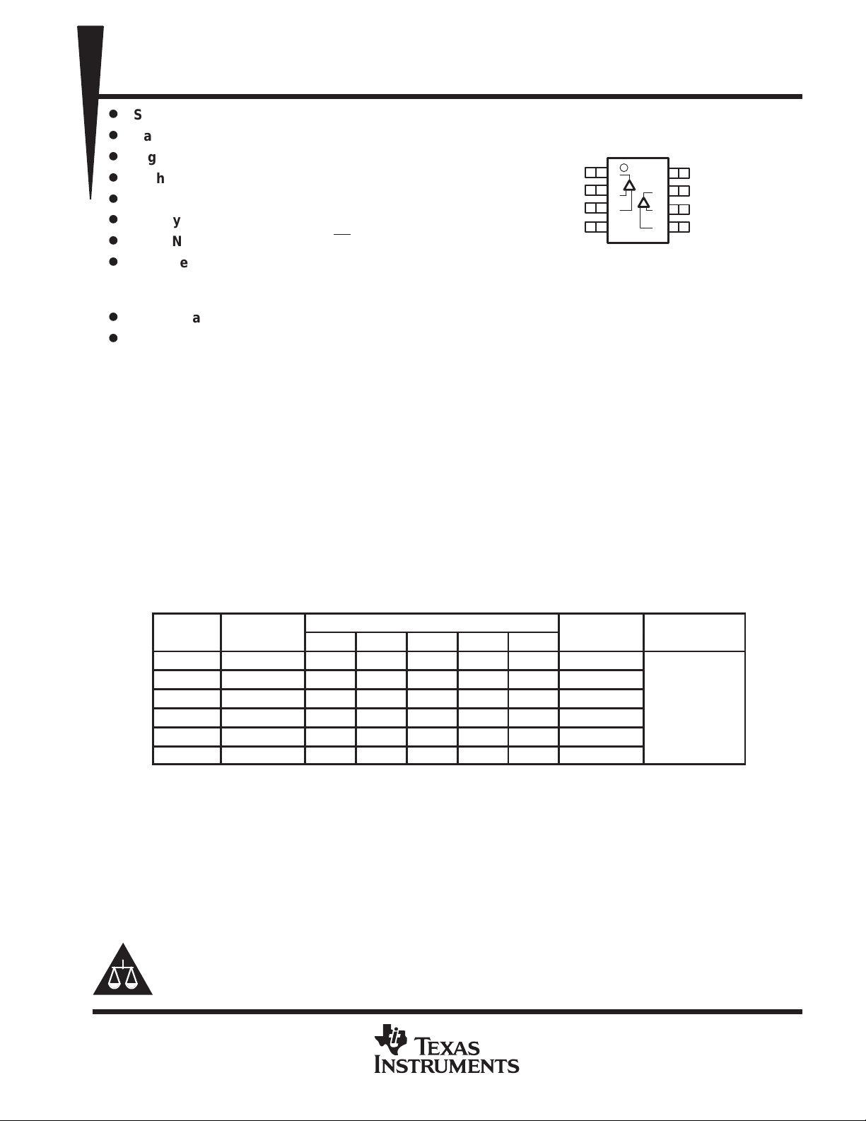
D, DGK, OR P PACKAGE
1OUT
1IN–
1IN+
GND
TLV2782
(TOP VIEW)
1
2
3
4
8
7
6
5
V
DD
2OUT
2IN–
2IN+
– 0°C to 70°C... Commercial Grade
– –40°C to 125°C... Industrial Grade
D
Ultra-Small Packaging
D
Universal Op Amp EVM
description
The TL V278x single supply operational amplifiers provide rail-to-rail input and output capability. The TLV278x
takes the minimum operating supply voltage down to 1.8 V over the extended industrial temperature range
(–40°C to 125°C) while adding the rail-to-rail output swing feature. The TL V278x also provides 8 MHz bandwidth
from only 650 µA of supply current. The maximum recommended supply voltage is 3.6 V, which allows the
devices to be operated from (±1.8 V supplies down to ±0.9 V) two rechargable cells.
The combination of wide bandwidth, low noise, and low distortion makes it ideal for high speed and high
resolution data converter applications. Its high output drive and bandwidth means that it is also suitable for video
line driving applications.
All members are available in PDIP , SOIC, and the newer , smaller SOT -23 (singles), MSOP (duals), and TSSOP
(quads).
FAMILY PACKAGE TABLE
NO. OF
CHANNELS
TLV2780
TLV2781
TLV2782 2 8 8 — — 8 —
TLV2783 2 14 14 — — 10 Yes
TLV2784
TLV2785
†
†
†
†
†
This device is in the Product Preview stage of development. Contact the local TI sales office for more
information.
1 8 8 6 — — Yes
1 8 8 5 — — —
4 14 14 — 14 — —
4 16 16 — 16 — Yes
PDIP SOIC SOT-23 TSSOP MSOP
PACKAGE TYPES
UNIVERSAL
EVM BOARD
Refer to the EVM
on Guide
Lit # SL
Please be aware that an important notice concerning availability, standard warranty, and use in critical applications of
Texas Instruments semiconductor products and disclaimers thereto appears at the end of this data sheet.
This document contains information on products in more than one phase
of development. The status of each device is indicated on the page(s)
specifying its electrical characteristics.
POST OFFICE BOX 655303 • DALLAS, TEXAS 75265
Copyright 2000, Texas Instruments Incorporated
1
TLV2780, TLV2781, TLV2782, TLV2783, TLV2784, TLV2785, TLV278xA
AT 25 C
3000 µV
AT 25 C
OUTLINE
†
DIP
DIP
40°C to 125°C
V
40°C to 125°C
FAMILY OF 1.8 V HIGH-SPEED RAIL-TO-RAIL INPUT/OUTPUT
OPERATIONAL AMPLIFIERS WITH SHUTDOWN
SLOS245 – MARCH 2000
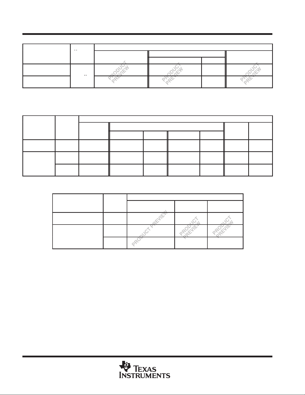
TLV2780 and TLV2781 AVAILABLE OPTIONS
T
A
0°C to 70°C
-40°C to 125°C
†
This package is available taped and reeled. To order this packaging option, add an R suffix to the part number (e.g., TLV2780CDR).
‡
This package is only available taped and reeled. For standard quantities (3,000 pieces per reel), add a R suffix (i.e., TL V2780CDBVR). For smaller
quantities (250 pieces per mini-reel), add a T suffix to the part number (e.g. TLV2780CDBVT).
T
A
0°C to 70°C 3000 µV
°
–
†
This package is available taped and reeled. To order this packaging option, add an R suffix to the part number (e.g., TLV2782CDR).
VIOmax
3000 µV
°
2000 µV
VIOmax
°
°
SMALL
(D)
TLV2782CD
TLV2783CD
TLV2782ID
TLV2783ID
TLV2782AID
TLV2783AID
SMALL OUTLINE
TLV2782 and TLV2783 AVAILABLE OPTIONS
†
(D)
TLV2780CD
TLV2781CD
TLV2780ID
TLV2781ID
†
(DGK)
TLV2782CDGK—xxTIAAI
TLV2782IDGK—xxTIAAJ
—
—
SYMBOL (DGS)
PACKAGED DEVICES
SOT-23
(DBV)‡ SYMBOL
TLV2780CDBV
TLV2781CDBV
TLV2780IDBV
TLV2781IDBV
PACKAGED DEVICES
MSOP
—
—
—
—
—
TLV2783CDGS—xxTIAAK
—
TLV2783IDGS—xxTIAAL—TLV2783IN
—
—
PLASTIC DIP
(P)
VAOC
VAPC
VAOI
VAPI
PLASTIC
†
SYMBOL
—
—
TLV2780IP
TLV2781IP
(N)
—
—
—
—
—
—
PLASTIC
(P)
—
—
TLV2782IP
—
—
—
TLV2784 and TLV2785 AVAILABLE OPTIONS
max
T
A
0°C to 70°C 3000 µV
°
–
†
This package is available taped and reeled. T o order this packaging option, add an R suffix to the part number
(e.g., TLV2784CDR).
°
IO
AT 25°C
3000 µV
2000 µV
SMALL OUTLINE
(D)
TLV2784CD
TLV2785CD
TLV2784ID
TLV2785ID
TLV2784AID
TLV2785AID
PACKAGED DEVICES
PLASTIC DIP
(N)
—
—
TLV2784IN
TLV2785IN
—
—
†
TSSOP
(PW)
TLV2784CPW
TLV2785CPW
TLV2784IPW
TLV2785IPW
TLV2784AIPW
TLV2785AIPW
2
POST OFFICE BOX 655303 • DALLAS, TEXAS 75265
TLV2780, TLV2781, TLV2782, TLV2783, TLV2784, TLV2785, TLV278xA
FAMILY OF 1.8 V HIGH-SPEED RAIL-TO-RAIL INPUT/OUTPUT
OPERATIONAL AMPLIFIERS WITH SHUTDOWN
SLOS245 – MARCH 2000
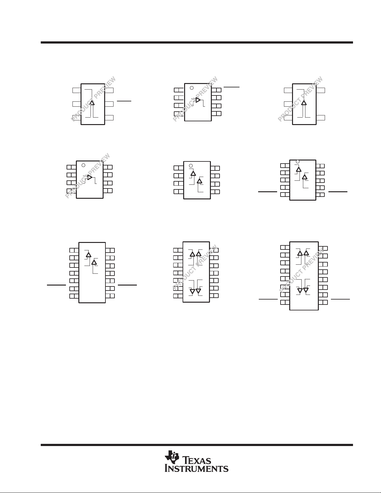
TLV278x PACKAGE PINOUTS
OUT
GND
IN+
D OR P PACKAGE
NC
IN–
IN+
GND
D OR N PACKAGE
TLV2780
DBV PACKAGE
(TOP VIEW)
1
6
2
5
3
4
TLV2781
(TOP VIEW)
1
2
3
4
(TOP VIEW)
8
7
6
5
TLV2783
V
DD
SHDN
IN–
NC
V
DD
OUT
NC
TLV2780
D OR P PACKAGE
(TOP VIEW)
NC
IN–
IN+
GND
D, DGK, OR P PACKAGE
1OUT
1IN–
1IN+
GND
1
2
3
4
TLV2782
(TOP VIEW)
1
2
3
4
TLV2784
D, N, OR PW PACKAGE
(TOP VIEW)
TLV2781
DBV PACKAGE
(TOP VIEW)
SHDN
8
V
7
6
5
8
7
6
5
DD
OUT
NC
V
DD
2OUT
2IN–
2IN+
OUT
GND
IN+
1OUT
1IN–
1IN+
GND
1SHDN
1
2
3
TLV2783
DGS PACKAGE
(TOP VIEW)
1
10
2
3
4
5
TLV2785
D, N, OR PW PACKAGE
(TOP VIEW)
V
5
4
9
8
7
6
DD
IN–
V
DD
2OUT
2IN–
2IN+
2SHDN
1OUT
1IN–
1IN+
GND
NC
1SHDN
NC
NC – No internal connection
1
14
2
13
3
12
4
11
5
10
6
7
1
V
DD
2OUT
2IN–
2IN+
NC
2SHDN
9
8
NC
1OUT
1IN–
1IN+
V
DD
2IN+
2IN–
2OUT
14
4OUT
2
13
4IN–
3
12
4IN+
4
11
GND
5
10
3IN+
6
7
9
3IN–
8
3OUT
1OUT
1IN–
1IN+
V
DD
2IN+
2IN–
2OUT
1SHDN
1
16
2
15
3
14
4
13
5
12
6
11
7
10
8
4OUT
4IN–
4IN+
GND
3IN+
3IN–
3OUT
9
2SHDN
POST OFFICE BOX 655303 • DALLAS, TEXAS 75265
3
TLV2780, TLV2781, TLV2782, TLV2783, TLV2784, TLV2785, TLV278xA
PACKAGE
JC
JA
A
Suppl
oltage, V
V
Operating free-air temperature, T
°C
‡
V
FAMILY OF 1.8 V HIGH-SPEED RAIL-TO-RAIL INPUT/OUTPUT
OPERATIONAL AMPLIFIERS WITH SHUTDOWN
SLOS245 – MARCH 2000
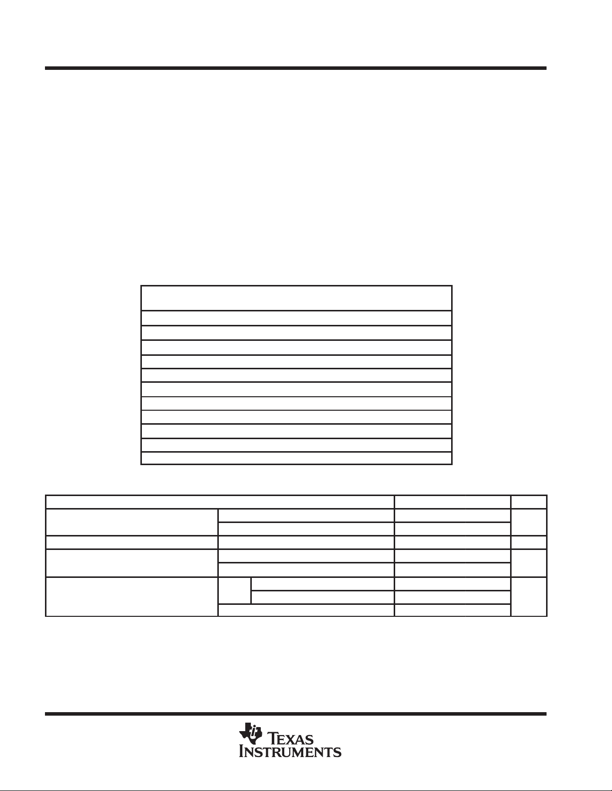
absolute maximum ratings over operating free-air temperature range (unless otherwise noted)
Supply voltage, VDD (see Note 1) 4 V. . . . . . . . . . . . . . . . . . . . . . . . . . . . . . . . . . . . . . . . . . . . . . . . . . . . . . . . . . . . .
Differential input voltage, VID ±V
Input current, I
(any input) ± 10 mA. . . . . . . . . . . . . . . . . . . . . . . . . . . . . . . . . . . . . . . . . . . . . . . . . . . . . . . . . . . . . .
I
Output current, IO ± 10 mA. . . . . . . . . . . . . . . . . . . . . . . . . . . . . . . . . . . . . . . . . . . . . . . . . . . . . . . . . . . . . . . . . . . . . .
Continuous total power dissipation See Dissipation Rating Table. . . . . . . . . . . . . . . . . . . . . . . . . . . . . . . . . . . . .
Operating free-air temperature range, TA: C suffix 0°C to 70°C. . . . . . . . . . . . . . . . . . . . . . . . . . . . . . . . . . . . . .
Maximum junction temperature, T
Storage temperature range, T
Lead temperature 1,6 mm (1/16 inch) from case for 10 seconds 260°C. . . . . . . . . . . . . . . . . . . . . . . . . . . . . . .
†
Stresses beyond those listed under “absolute maximum ratings” may cause permanent damage to the device. These are stress ratings only, and
functional operation of the device at these or any other conditions beyond those indicated under “recommended operating conditions” is not
implied. Exposure to absolute-maximum-rated conditions for extended periods may affect device reliability.
NOTE 1: All voltage values, except differential voltages, are with respect to GND.
D (8) 38.3 176 710 mW
D (14) 26.9 122.3 1022 mW
D (16) 25.7 114.7 1090 mW
DBV (5) 55 324.1 385 mW
DBV (6) 55 294.3 425 mW
DGK (8) 54.23 259.96 481 mW
DGS (10) 54.1 257.71 485 mW
N (14, 16) 32 78 1600 mW
P (8) 41 104 1200 mW
PW (14) 29.3 173.6 720 mW
PW (16) 28.7 161.4 774 mW
. . . . . . . . . . . . . . . . . . . . . . . . . . . . . . . . . . . . . . . . . . . . . . . . . . . . . . . . . . . . . . .
I suffix –40°C to 125°C. . . . . . . . . . . . . . . . . . . . . . . . . . . . . . . . . . . .
150°C. . . . . . . . . . . . . . . . . . . . . . . . . . . . . . . . . . . . . . . . . . . . . . . . . . . . . . . . .
J
–65°C to 150°C. . . . . . . . . . . . . . . . . . . . . . . . . . . . . . . . . . . . . . . . . . . . . . . . . . .
stg
DISSIPATION RATING TABLE
Θ
(°C/W)
Θ
(°C/W)
T
≤ 25°C
POWER RATING
†
DD
recommended operating conditions
pp
y v
Common-mode input voltage range, V
p
Shutdown on/off voltage level
‡
Relative to GND.
4
DD
MIN MAX UNIT
Single supply 1.8 3.6
Split supply ±0.9 ±1.8
ICR
p
A
C-suffix 0 70
I-suffix –40 125
VDD < 2.7 V 0.75V
IH
VDD = 2.7 to 3.6 V 2
V
IL
POST OFFICE BOX 655303 • DALLAS, TEXAS 75265
–0.2 VDD+0.2 V
°
DD
V
0.6
,
TLV278
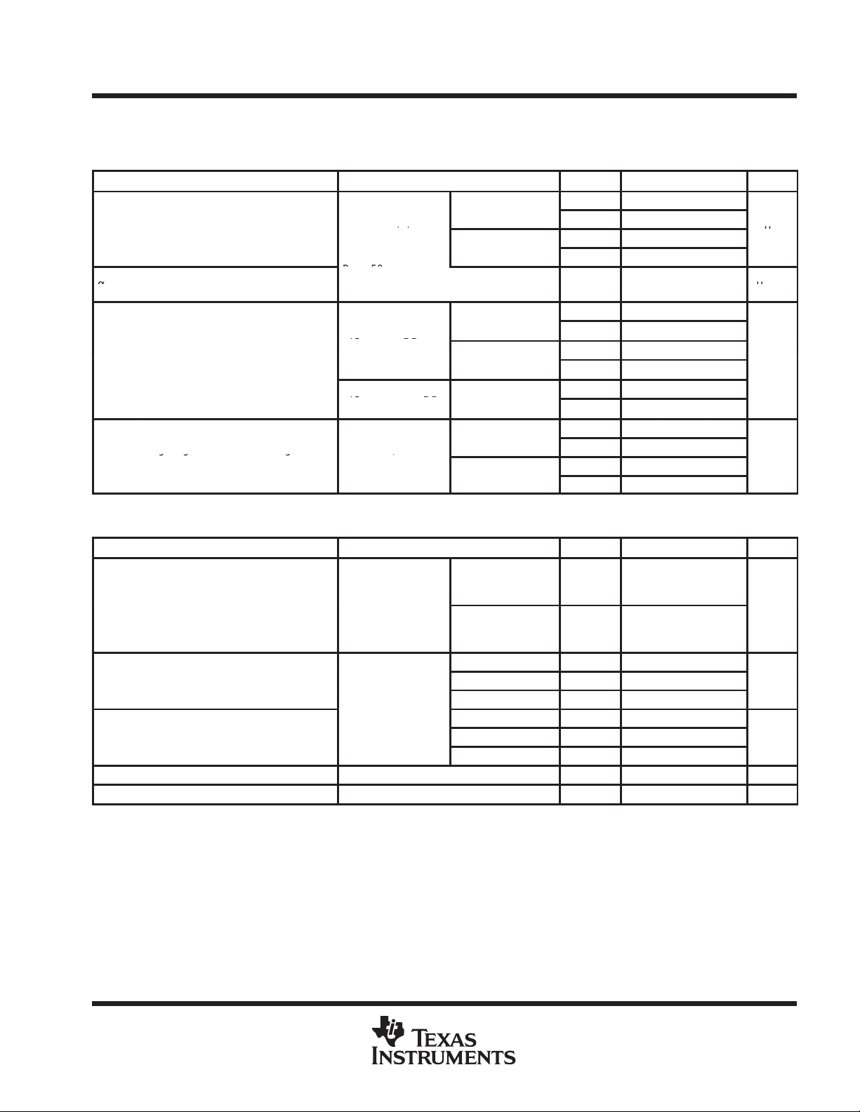
VIOInput offset voltage
V
IC
VDD/2,
V
TLV278xA
8µV/°C
V
1.8 V
IC DD
CMRR
Common-mode rejection ratio
V
2.7 V/ 3.6 V
dB
IC DD
V
2.7 V/ 3.6 V
V
V
A
gg g
L
,
V/mV
V
2.7 V/ 3.6 V
V
Common-mode input voltage range
CMRR
V
V
IC
VDD/2
ODD
TLV2780, TLV2781, TLV2782, TLV2783, TLV2784, TLV2785, TLV278xA
FAMILY OF 1.8 V HIGH-SPEED RAIL-TO-RAIL INPUT/OUTPUT
OPERATIONAL AMPLIFIERS WITH SHUTDOWN
SLOS245 – MARCH 2000
electrical characteristics at specified free-air temperature, VDD = 1.8 V, 2.7 V (unless otherwise
noted)
dc performance
PARAMETER TEST CONDITIONS
DD
DD
DD
DD
DD
x
=
=
=
= 1.8
=
V
= V
/2
p
α
†
Temperature coefficient of input offset
VIO
voltage
Large-signal differential voltage R
VD
amplification
Full range is 0°C to 70°C for the C suffix and –40°C to 125°C for the I suffix. If not specified, full range is –40°C to 125°C.
VO = VDD/2,
RL = 2 kΩ,
RS = 50 Ω
VIC = 0 to VDD,
RS = 50 Ω
VIC = 1.2 V to VDD,
RS = 50 Ω
= 2 kΩ,
V
= 1 V
O(PP)
†
T
A
25°C 250 3000
Full range 4500
25°C 250 2000
Full range 3000
25°C 50 76
Full range 50
25°C 55 80
Full range 50
25°C 70 100
Full range 70
25°C 200 600
Full range 50
25°C 200 1000
Full range 70
MIN TYP MAX
UNIT
µ
°
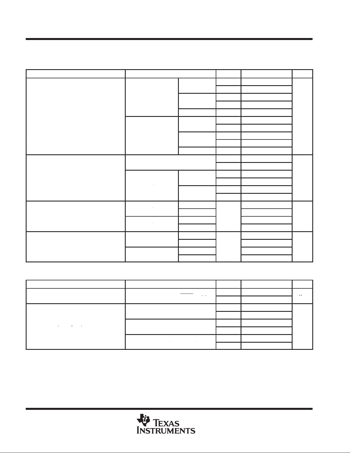
input characteristics
PARAMETER TEST CONDITIONS
ICR
I
I
r
C
†
Input offset current
IO
Input bias current
IB
Differential input resistance 25°C 1000 GΩ
i(d)
Common-mode input capacitance f = 1 kHz 25°C 2.8 pF
i(c)
Full range is 0°C to 70°C for the C suffix and –40°C to 125°C for the I suffix. If not specified, full range is –40°C to 125°C.
p
Measured over
range,
RS = 50 Ω
=
=
VO = VDD/2,
RL = 2 kΩ,
RS = 50 Ω
,
VDD = 1.8 V
VDD = 2.7 V
TLV278xC Full range 100
TLV278xI Full range 300
TLV278xC Full range 100
TLV278xI Full range 300
†
T
A
25°C or
full range
25°C or-
Full range
25°C 2.5 15
25°C 2.5 15
MIN TYP MAX
–0.2
to
2
–0.2
to
2.9
UNIT
pA
pA
POST OFFICE BOX 655303 • DALLAS, TEXAS 75265
5
TLV2780, TLV2781, TLV2782, TLV2783, TLV2784, TLV2785, TLV278xA
V
V
I
OH
mA
V
2.7 V
VOHHigh-level output voltage
V
V
V
I
OH
mA
V
V
IC DD
,
VOLLow-level output voltage
V
V
mV
IC DD
,
V
V
DD
,
IOOutput current
25°C17mA
DD
,
Sourcing
IOSShort-circuit output current
25°C21mA
Sinking
IDDSupply current (per channel)
V
VDD/2
SHDN
V
A
DD
,
,
k
ygj
DD
,
,
dB
DD
,
,
FAMILY OF 1.8 V HIGH-SPEED RAIL-TO-RAIL INPUT/OUTPUT
OPERATIONAL AMPLIFIERS WITH SHUTDOWN
SLOS245 – MARCH 2000
electrical characteristics at specified free-air temperature, VDD = 1.8 V, 2.7 V (unless otherwise
noted) (continued)
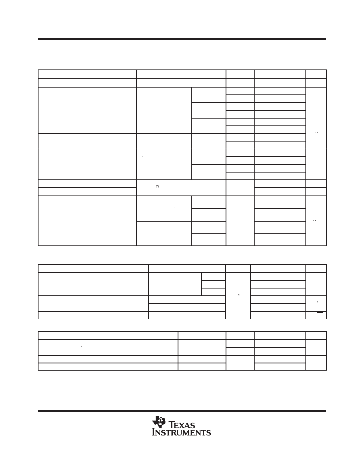
output characteristics
PARAMETER TEST CONDITIONS
= 1.8
DD
VIC = VDD/2,
= –1
–
p
VIC = VDD/2,
= –5
–
V
= V
= V
= 1.8 V,
= 2.7 V,
/2,
/2,
IOL = 1 mA
p
p
p
†
Full range is 0°C to 70°C for the C suffix and –40°C to 125°C for the I suffix. If not specified, full range is –40°C to 125°C.
V
IOL = 5 mA
V
VO = 0.5 V from
V
VO = 0.5 V from
=
DD
VDD = 3.6 V 25°C 3.58
= 1.8
DD
= 2.7
DD
VDD = 3.6 V 25°C 3.55
= 1.8
DD
= 2.7
DD
Positive rail 10
Negative rail
Positive rail
Negative rail 23
VDD = 1.8 V 13
VDD = 2.7 V
VDD = 1.8 V
VDD = 2.7 V 45
†
T
A
25°C 1.7 1.77
Full range 1.63
25°C 2.6 2.68
Full range 2.6
25°C 1.5 1.55
Full range 1.46
25°C 2.5 2.55
Full range 2.45
25°C 70
Full range 80
25°C 180 240
Full range 290
25°C 120 170
Full range 200
°
°
MIN TYP MAX
15
35
UNIT
power supply
pp
Supply voltage rejection ratio V
SVR
(∆VDD /∆VIO)
†
Full range is 0°C to 70°C for the C suffix and –40°C to 125°C for the I suffix. If not specified, full range is –40°C to 125°C.
6
PARAMETER TEST CONDITIONS
p
=
O
V
VIC = VDD/2
VIC = VDD/2
V
VIC = VDD/2
POST OFFICE BOX 655303 • DALLAS, TEXAS 75265
,
= 1.8 V to 2.7 V, No load,
= 2.7 V to 3.6 V, No load,
= 1.8 V to 3.6 V, No load,
=
DD
Full range
Full range 58
Full range 70
Full range 60
†
T
A
25°C 650 770
25°C 60 75
25°C 75 90
25°C 65 80
MIN TYP MAX
820
UNIT
µ
V
V
SR+Positive slew rate at unity gain
R
C
V
2.7 V
C
L
F
V
V
V/µs
V
V
SR–Negative slew rate at unity gain
R
V
2.7 V
C
L
F
V
V
R
2 kΩ
C
25 pF
25°C
(STEP)PP
,
tsSettling time
25°C
s
(STEP)PP
,
V
O(PP)
VDD/2
25°C
VnEquivalent input noise voltage
V/√H
I
y,
SHDN
V
nA
25°C
ns
TLV2780, TLV2781, TLV2782, TLV2783, TLV2784, TLV2785, TLV278xA
FAMILY OF 1.8 V HIGH-SPEED RAIL-TO-RAIL INPUT/OUTPUT
OPERATIONAL AMPLIFIERS WITH SHUTDOWN
SLOS245 – MARCH 2000
electrical characteristics at specified free-air temperature, VDD = 1.8 V, 2.7 V (unless otherwise
noted) (continued)
dynamic performance
PARAMETER TEST CONDITIONS
UGBW Unity gain bandwidth
φ
m
†
Full range is 0°C to 70°C for the C suffix and –40°C to 125°C for the I suffix. If not specified, full range is –40°C to 125°C.
Phase margin
Gain margin
RL = 2 kΩ,C
V
= 1 V,
O(PP)
= 2 kΩ,
L
= 50 pF
= 50
V
= 1 V,
O(PP)
= 2 kΩ,
L
= 50 pF
C
= 50
,
=
L
VDD = 1.8 V,
V
AV = –1,
CL = 10 pF, RL = 2 kΩ
VDD = 2.7 V,
V
AV = –1,
CL = 10 pF, RL = 2 kΩ
= 1 V,
= 1 V,
= 25 pF
L
= 1.8
DD
=
DD
= 3.6
DD
= 1.8
DD
=
DD
= 3.6
DD
p
=
L
0.1% 1.7
0.01%
0.1%
0.01% 2.4
†
T
A
25°C 8 MHz
25°C
Full range 3.1
25°C
Full range 3.5
25°C
Full range 3.6
25°C
Full range 1.89
25°C
Full range 1.97
25°C
Full range 3.4
°
°
MIN TYP MAX UNIT
3.3 4.3
3.8 4.8
4 5
2.1 2.8
2.2 2.8
3.5 4.2
58°
8 dB
2.8
1.7
µ
noise/distortion performance
PARAMETER TEST CONDITIONS
THD + N Total harmonic distortion plus noise
p
I
n
Equivalent input noise current f = 1 kHz 0.9
T
A
=
=
RL = 2 kΩ,
f = 10 kHz
f = 1 kHz
f = 10 kHz 9
,
AV = 1 0.055%
AV = 10 0.08%
AV = 100
MIN TYP MAX
0.45%
18
UNIT
n
fA/√Hz
shutdown characteristics
PARAMETER TEST CONDITIONS
DD(SHDN)
t
(on)
t
(off)
†
Full range is 0°C to 70°C for the C suffix and –40°C to 125°C for the I suffix. If not specified, full range is –40°C to 125°C.
‡
Disable time and enable time are defined as the interval between application of the logic signal to SHDN and the point at which the supply current
has reached half its final value.
Supply current, all channels in shutdown mode
(TLV2780, TLV2783, TLV2785)
Amplifier turnon time
Amplifier turnoff time
‡
‡
= 0
RL = 2 kΩ
RL = 2 kΩ
†
T
A
25°C 900 1400
Full range 1700
°
MIN TYP MAX
800
200
UNIT
z
POST OFFICE BOX 655303 • DALLAS, TEXAS 75265
7
TLV2780, TLV2781, TLV2782, TLV2783, TLV2784, TLV2785, TLV278xA
SR
Slew rate
FAMILY OF 1.8 V HIGH-SPEED RAIL-TO-RAIL INPUT/OUTPUT
OPERATIONAL AMPLIFIERS WITH SHUTDOWN
SLOS245 – MARCH 2000
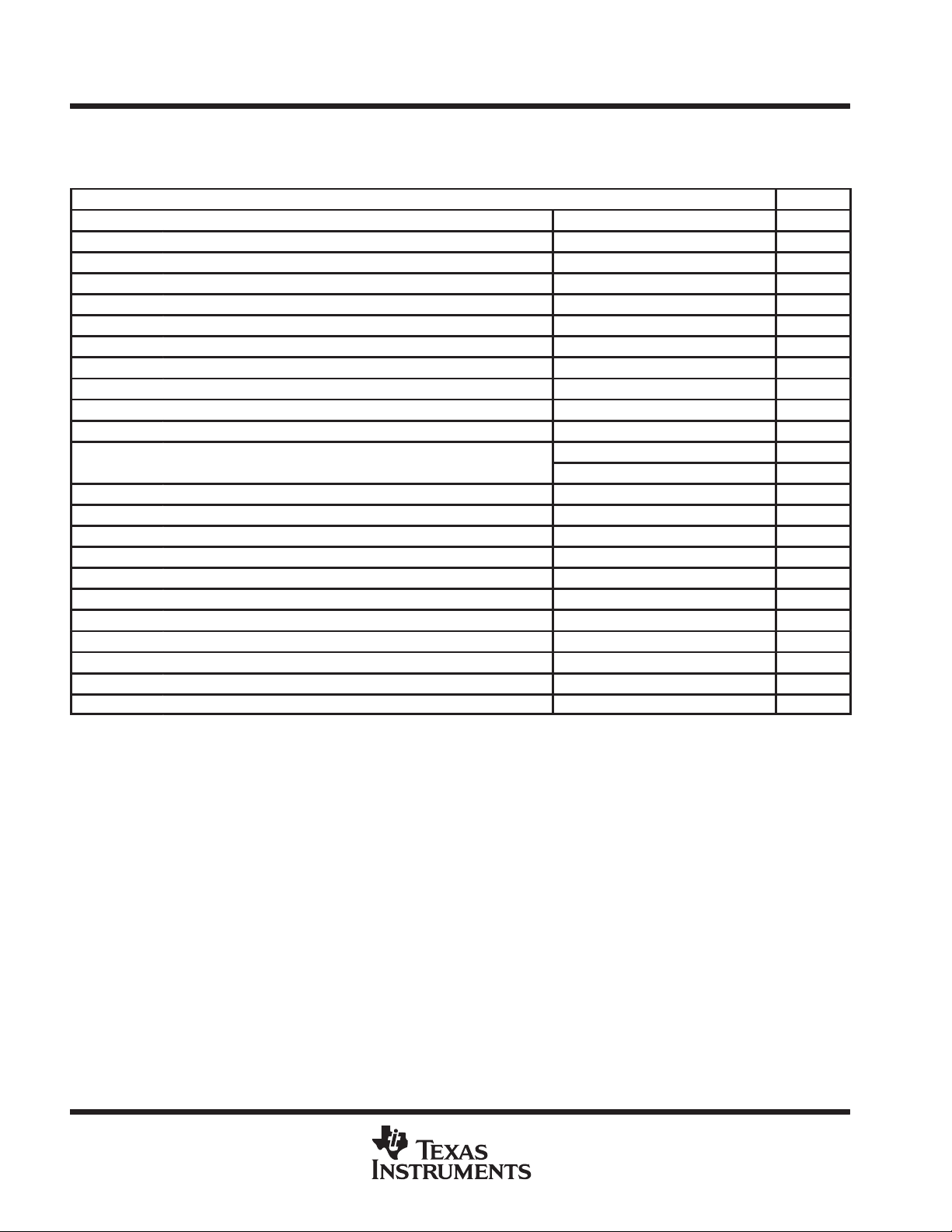
TYPICAL CHARACTERISTICS
Table of Graphs
FIGURE
V
IO
CMRR Common-mode rejection ratio vs Frequency 3
V
OH
V
OL
V
O(PP)
Z
o
I
DD
I
DD
PSRR Power supply rejection ratio vs Frequency 12
A
VD
φ
m
V
n
I
DD(SHDN)
I
DD(SHDN)
I
DD(SHDN)
Input offset voltage vs Common-mode input voltage 1, 2
High-level output voltage vs High-level output current 4, 6
Low-level output voltage vs Low-level output current 5, 7
Maximum peak-to-peak output voltage vs Frequency 8
Output impedance vs Frequency 9
Supply current vs Supply voltage 10
Supply current vs Free-air temperature 11
Differential voltage amplification & phase vs Frequency 13
Gain-bandwidth product vs Free-air temperature 14
vs Supply voltage 15
vs Free-air temperature 16, 17
Phase margin vs Load capacitance 18
Equivalent input noise voltage vs Frequency 19
Voltage-follower large-signal pulse response vs Time 20
Voltage-follower small-signal pulse response vs Time 21
Inverting large-signal pulse response vs Time 22
Inverting small-signal pulse response vs Time 23
Crosstalk vs Frequency 24
Shutdown forward & reverse isolation vs Frequency 25
Shutdown supply current vs Free-air temperature 26
Shutdown supply current vs Supply voltage 27
Shutdown supply current/output voltage vs Time 28
8
POST OFFICE BOX 655303 • DALLAS, TEXAS 75265
 Loading...