

Texas Instruments TLC7733IPWR, TLC7733IPWLE, TLC7733IDR, TLC7725QPWLE, TLC7725QPWR Datasheet
...
TLC7701, TLC7725, TLC7703, TLC7733, TLC7705
MICROPOWER SUPPLY VOLTAGE SUPERVISORS
SLVS087K – DECEMBER 1994 – REVISED JULY 1999
1
POST OFFICE BOX 655303 • DALLAS, TEXAS 75265
D
Power-On Reset Generator
D
Automatic Reset Generation After
Voltage Drop
D
Precision V oltage Sensor
D
T emperature-Compensated Voltage
Reference
D
Programmable Delay Time by External
Capacitor
D
Supply Voltage Range ...2 V to 6 V
D
Defined RESET Output from VDD ≥1 V
D
Power-Down Control Support for Static
RAM With Battery Backup
D
Maximum Supply Current of 16 µA
D
Power Saving Totem-Pole Outputs
D
T emperature Range ...–40°C to 125°C
description
The TLC77xx family of micropower supply voltage
supervisors provide reset control, primarily in
microcomputer and microprocessor systems.
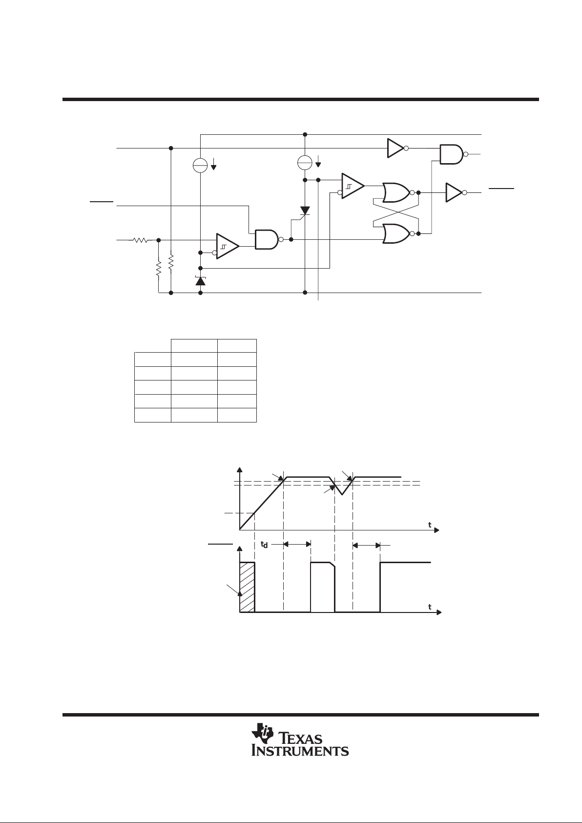
During power-on, RESET is asserted when V
DD
reaches 1 V. After minimum VDD (≥ 2 V) is
established, the circuit monitors SENSE voltage
and keeps the reset outputs active as long as
SENSE voltage (V
I(SENSE)
) remains below the
threshold voltage. An internal timer delays return
of the output to the inactive state to ensure proper
system reset. The delay time, t
d
, is determined by
an external capacitor:
td = 2.1 × 10⁴ × C
T
Where
CT is in farads
t
d
is in seconds
Except for the TLC7701, which can be customized with two external resistors, each supervisor has a fixed
SENSE threshold voltage set by an internal voltage divider . When SENSE voltage drops below the threshold
voltage, the outputs become active and stay in that state until SENSE voltage returns above threshold voltage
and the delay time, td, has expired.
Please be aware that an important notice concerning availability, standard warranty, and use in critical applications of
Texas Instruments semiconductor products and disclaimers thereto appears at the end of this data sheet.
PRODUCTION DATA information is current as of publication date.
Products conform to specifications per the terms of Texas Instruments
standard warranty. Production processing does not necessarily include
testing of all parameters.
Copyright 1999, Texas Instruments Incorporated
1
2
3
4
8
7
6
5
CONTROL
RESIN
CT
GND
V
DD
SENSE
RESET
RESET
D, JG, P OR PW PACKAGE
(TOP VIEW)
3212019
910111213
4
5
6
7
8
18
17
16
15
14
NC
SENSE
NC
RESET
NC
NC
RESIN
NC
CT
NC
NC
CONTROL
NC
RESET
NC
NC
NC
NC
V
DD
FK PACKAGE
(TOP VIEW)
GND
1
2
3
4
5
10
9
8
7
6
NC
CONTROL
RESIN
CT
GND
NC
V
DD
SENSE
RESET
RESET
U PACKAGE
(TOP VIEW)
TLC7701, TLC7725, TLC7703, TLC7733, TLC7705
MICROPOWER SUPPLY VOLTAGE SUPERVISORS
SLVS087K – DECEMBER 1994 – REVISED JULY 1999
2
POST OFFICE BOX 655303 • DALLAS, TEXAS 75265
description (continued)
In addition to the power-on-reset and undervoltage-supervisor function, the TLC77xx adds power-down control
support for static RAM. When CONTROL is tied to GND, RESET will act as active high. The voltage monitor
contains additional logic intended for control of static memories with battery backup during power failure. By
driving the chip select (CS
) of the memory circuit with the RESET output of the TLC77xx and with the CONTROL
driven by the memory bank select signal (CSH1
) of the microprocessor (see Figure 10), the memory circuit is
automatically disabled during a power loss. (In this application the TLC77xx power has to be supplied by the
battery.)
The TLC77xxI is characterized for operation over a temperature range of –40°C to 85°C; the TLC77xxQ is
characterized for operation over a temperature range of –40°C to 125°C; and the TLC77xxM is characterized
for operation over the full Military temperature range of –55°C to 125°C.
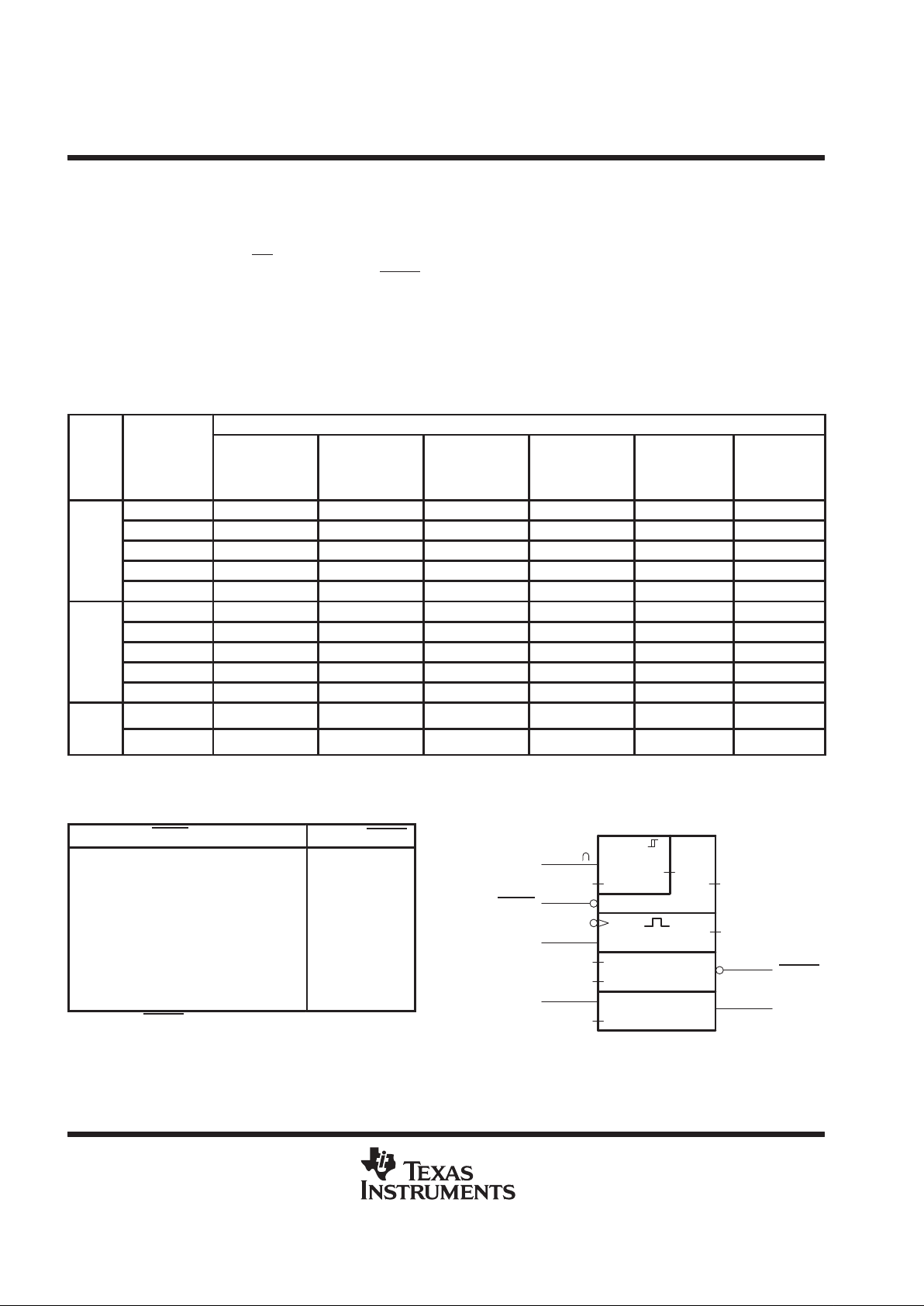
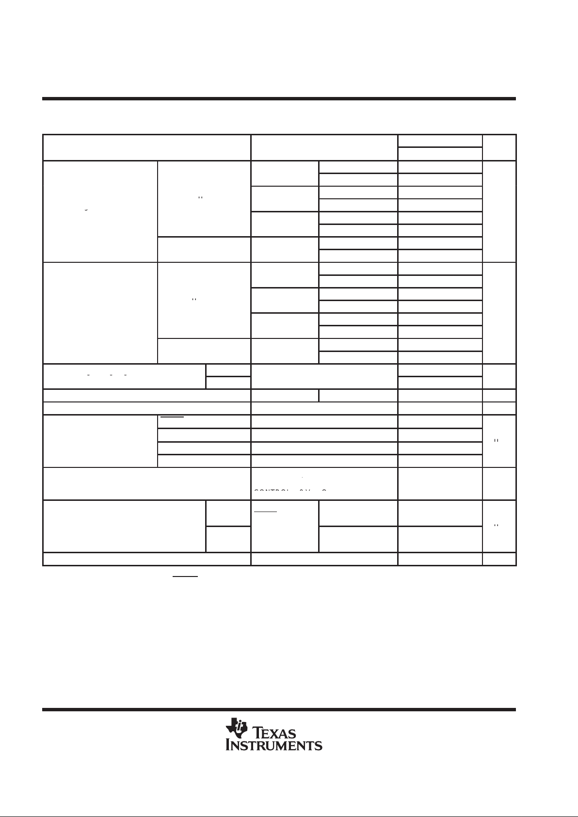
AVAILABLE OPTIONS
PACKAGED DEVICES
T
A
THRESHOLD
VOLTAGE
(V)
SMALL
OUTLINE (D)
†
CHIP
CARRIER (FK)
CERAMIC DIP
(JG)
CERAMIC
DUAL
FLATPACK
(U)
PLASTIC DIP
(P)
THIN SHRINK
SMALL
OUTLINE
(PW)
‡
1.1 TLC7701ID — — — TLC7701IP TLC7701IPW
–
°
2.25 TLC7725ID — — — TLC7725IP TLC7725IPW
40 C
to
2.63 TLC7703ID — — — TLC7703IP TLC7703IPW
85°C
2.93 TLC7733ID — — — TLC7733IP TLC7733IPW
4.55 TLC7705ID — — — TLC7705IP TLC7705IPW
1.1 TLC7701QD — — — TLC7701QP TLC7701QPW
–
°
2.25 TLC7725QD — — — TLC7725QP TLC7725QPW
40 C
to
2.63 TLC7703QD — — — TLC7703QP TLC7703QPW
125°C
2.93 TLC7733QD — — — TLC7733QP TLC7733QPW
4.55 TLC7705QD — — — TLC7705QP TLC7705QPW
–55°C
2.93 — TLC7733MFK TLC7733MJG — — —
to
125°C
4.55 — TLC7705MFK TLC7705MJG TLC7705MU — —
†
The D package is available taped and reeled. Add the suffix R to the device type when ordering (e.g., TLC7705QDR).
‡
The PW package is only available left-end taped and reeled (indicated by the LE suffix on the device type; e.g., TLC7705QPWLE).
FUNCTION TABLE
CONTROL
RESIN
V
I(SENSE)>VIT+
RESET
RESET
L L False H L
L L True H L
L H False H L
L H True L
§
H
§
H L False H L
H L True H L
H H False H L
H H True H H
§
§
RESET and RESET states shown are valid for t > td.
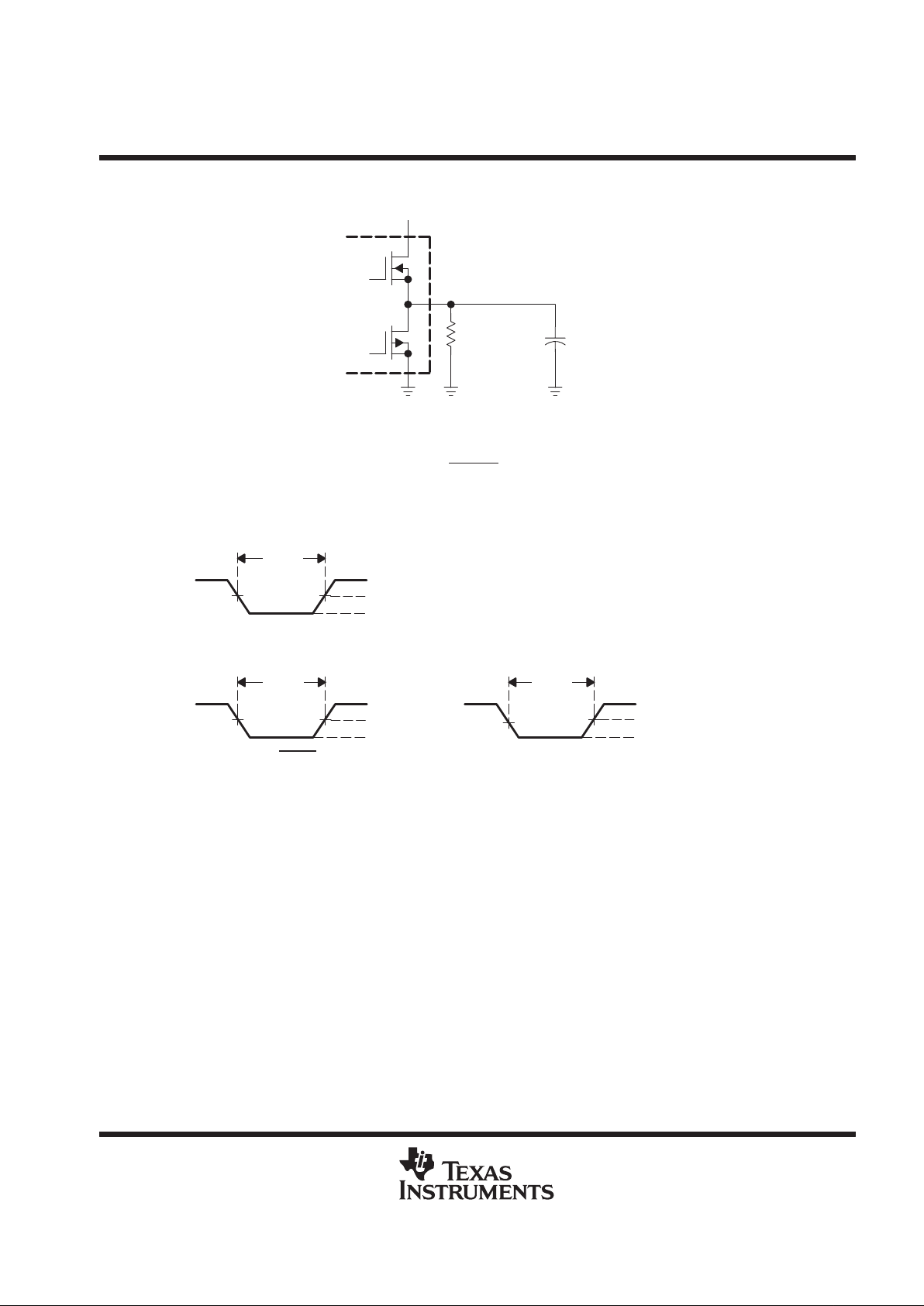
logic symbol
¶
¶
This symbol is in accordance with ANSI/IEEE Std 91–1984 and
IEC Publication 617-12.
6
1
3
2
7
SENSE
≥1
≥1
≥1
RESET
5
COMP
S
V
IT
S<V
IT
Z1
Z2
Z3
RESIN
CT
CONTROL
RESET
3
2
1
1
CX×
TLC7701, TLC7725, TLC7703, TLC7733, TLC7705
MICROPOWER SUPPLY VOLTAGE SUPERVISORS
SLVS087K – DECEMBER 1994 – REVISED JULY 1999
3
POST OFFICE BOX 655303 • DALLAS, TEXAS 75265
functional block diagram
1.1 V
R2
‡
R1
‡
RESET
†
RESET
†
V
DD
GND
8
6
5
4
RESIN
CONTROL
SENSE
CT
3
1
2
7
1 MΩ
50 µA
†
Outputs are totem-pole configuration. External pullup or pulldown resistors are not required.
‡
Nominal values:
TLC7701
TLC7703
R1 (Typ) R2 (Typ)
TLC7733
TLC7705
750 k
910 k 290 k
450 kΩ
Ω
Ω
Ω
0
∞
502 kΩ698 kΩ
TLC7725 600 k 600 k
ΩΩ
timing diagram
RESET
Output
Output
Undefined
VDD and V
I(SENSE)
t
d
Threshold Voltages
V
res
V
IT–
V
IT+
t
d
t
t
V
IT+
TLC7701, TLC7725, TLC7703, TLC7733, TLC7705
MICROPOWER SUPPLY VOLTAGE SUPERVISORS
SLVS087K – DECEMBER 1994 – REVISED JULY 1999
4
POST OFFICE BOX 655303 • DALLAS, TEXAS 75265
absolute maximum ratings over operating free-air temperature (unless otherwise noted)
†
Supply voltage, VDD (see Note 1) 7 V. . . . . . . . . . . . . . . . . . . . . . . . . . . . . . . . . . . . . . . . . . . . . . . . . . . . . . . . . . . .
Input voltage range, CONTROL, RESIN, SENSE (see Note 1) –0.3 V to 7 V. . . . . . . . . . . . . . . . . . . . . . . . . . .
Maximum low output current, IOL 10 mA. . . . . . . . . . . . . . . . . . . . . . . . . . . . . . . . . . . . . . . . . . . . . . . . . . . . . . . . . .
Maximum high output current, I
OH
–10 mA. . . . . . . . . . . . . . . . . . . . . . . . . . . . . . . . . . . . . . . . . . . . . . . . . . . . . . . .
Input clamp current, IIK (VI < 0 or VI > VDD) ±10 mA. . . . . . . . . . . . . . . . . . . . . . . . . . . . . . . . . . . . . . . . . . . . . .
Output clamp current, IOK (VO < 0 or VO > VDD) ±10 mA. . . . . . . . . . . . . . . . . . . . . . . . . . . . . . . . . . . . . . . . . . .
Continuous total power dissipation See Dissipation Rating Table. . . . . . . . . . . . . . . . . . . . . . . . . . . . . . . . . . . .
Operating free-air temperature range, TA: TL77xxI –40°C to 85°C. . . . . . . . . . . . . . . . . . . . . . . . . . . . . . . . . . . .
TL77xxQ –40°C to 125°C. . . . . . . . . . . . . . . . . . . . . . . . . . . . . . . . . .
TL77xxM –55°C to 125°C. . . . . . . . . . . . . . . . . . . . . . . . . . . . . . . . . .
Storage temperature range, T
stg
–65°C to 150°C. . . . . . . . . . . . . . . . . . . . . . . . . . . . . . . . . . . . . . . . . . . . . . . . . .
†
Stresses beyond those listed under “absolute maximum ratings” may cause permanent damage to the device. These are stress ratings only, and
functional operation of the device at these or any other conditions beyond those indicated under “recommended operating conditions” is not
implied. Exposure to absolute-maximum-rated conditions for extended periods may affect device reliability.
NOTE 1: All voltage values are with respect to GND.
DISSIPATION RATING TABLE
PACKAGE
TA ≤ 25°C
POWER RATING
DERATING FACTOR
ABOVE TA = 25°C
TA = 85°C
POWER RATING
TA = 125°C
POWER RATING
D 725 mW 5.8 mW/°C 377 mW 145 mW
FK 1375 mW 11.0 mW/°C 715 mW 275 mW
JG 1050 mW 8.4 mW/°C 546 mW 210 mW
P 1000 mW 8.0 mW/°C 520 mW 200 mW
PW 525 mW 4.2 mW/°C 273 mW 105 mW
U 700 mW 5.5 mW/°C 370 mW 150 mW
recommended operating conditions at specified temperature range
MIN MAX UNIT
Supply voltage, V
DD
2 6 V
Input voltage, V
I
0 V
DD
V
High-level input voltage at RESIN and CONTROL‡, V
IH
0.7×V
DD
V
Low-level input voltage at RESIN and CONTROL‡, V
IL
0.2×V
DD
V
High-level output current, I
OH
–2 mA
Low-level output current, I
OL
V
DD
≥ 2.7 V
2 mA
Input transition rise and fall rate at RESIN and CONTROL, ∆t/∆V 100 ns/V
p
p
TLC77xxI –40 85
°
Operating free-air temperature range, T
A
TLC77xxQ –40 125
°C
Operating free-air temperature range, T
A
TLC77xxM –55 125 °C
‡
To ensure a low supply current, VIL should be kept <0.3 V and VIH > VDD –0.3 V.
TLC7701, TLC7725, TLC7703, TLC7733, TLC7705
MICROPOWER SUPPLY VOLTAGE SUPERVISORS
SLVS087K – DECEMBER 1994 – REVISED JULY 1999
5
POST OFFICE BOX 655303 • DALLAS, TEXAS 75265
electrical characteristics over recommended operating conditions (see Note 2) (unless otherwise
noted)
TLC77xx
PARAMETER
TEST CONDITIONS
MIN
TYP
†
MAX
UNIT
VDD = 2 V 1.8
p
IOH = –20 µA
VDD = 2.7 V 2.5
VOHHigh-level output voltage
VDD = 4.5 V 4.3
V
IOH = –2 mA VDD = 4.5 V 3.7
VDD = 2 V 0.2
p
IOL = 20 µA
VDD = 2.7 V 0.2
VOLLow-level output voltage
VDD = 4.5 V 0.2
V
IOL = 2 mA VDD = 4.5 V 0.5
TLC7701 1.04 1.1 1.16
TLC7725 2.18 2.25 2.32
V
IT–
Negative-going input threshold voltage,
TLC7703
VDD = 2 V to 6 V
2.56 2.63 2.70
V
SENSE (see Note 3)
TLC7733 2.86 2.93 3
TLC7705 4.47 4.55 4.63
TLC7701 VDD = 2 V to 6 V 30 mV
TLC7725
V
hys
Hysteresis voltage, SENSE
TLC7703,
y
TLC7733,
V
DD
=
2 V to 6 V
70
mV
TLC7705
V
res
Power-up reset voltage
‡
IOL = 20 µA 1 V
RESIN
VI = 0 V to V
DD
2
p
CONTROL
VI = V
DD
7 15
I
I
Input current
SENSE VI = 5 V 5 10
µA
SENSE, TLC7701 only VI = 5 V 2
RESIN = V
,
I
DD
Supply current
RESIN VDD,
SENSE = VDD ≥ VITmax + 0.2 V
916µA
CONTROL = 0 V, Outputs open
I
DD(d)
Supply current during t
d
VDD = 5 V,
RESIN
= VDD,
CONTROL = 0 V,
VCT = 0 ,
SENSE = VDD,
Outputs open
120 150 µA
C
I
Input capacitance, SENSE VI = 0 V to V
DD
50 pF
†
Typical values apply at TA = 25°C.
‡
The lowest supply voltage at which RESET
becomes active. The symbol V
res
is not currently listed within EIA or JEDEC standards for
semiconductor symbology . Rise time of VDD ≥ 15 µs/V.
NOTES: 2. All characteristics are measured with CT = 0.1 µF.
3. T o ensure best stability of the threshold voltage, a bypass capacitor (ceramic, 0.1 µF) should be connected near the supply terminals.
TLC7701, TLC7725, TLC7703, TLC7733, TLC7705
MICROPOWER SUPPLY VOLTAGE SUPERVISORS
SLVS087K – DECEMBER 1994 – REVISED JULY 1999
6
POST OFFICE BOX 655303 • DALLAS, TEXAS 75265
electrical characteristics over recommended operating conditions (see Note 2) (unless otherwise
noted)
TLC77xxM
PARAMETER
TEST CONDITIONS
MIN
TYP
†
MAX
UNIT
TA = 25°C 1.8
V
DD
=
2 V
,
TA = –55°C to 125°C 1.7
TA = 25°C 2.5
High-level output
I
OH
= –
20 µA
V
DD
=
2.7 V
TA = –55°C to 125°C 2.3
V
OH
g
voltage
TA = 25°C 4.3
V
V
DD
= 4.5
V
TA = –55°C to 125°C 4.2
TA = 25°C 3.7
I
OH
= –2
mA
V
DD
= 4.5
V
TA = –55°C to 125°C 3.6
TA = 25°C 0.2
V
DD
=
2 V
TA = –55°C to 125°C 0.2
TA = 25°C 0.2
Low-level output
I
OL
= 20 µ
A
V
DD
= 2.7
V
TA = –55°C to 125°C 0.2
V
OL
voltage
TA = 25°C 0.2
V
V
DD
= 4.5
V
TA = –55°C to 125°C 0.2
TA = 25°C 0.5
I
OL
=
2 mA
V
DD
=
4.5 V
TA = –55°C to 125°C 0.5
Negative-going input threshold
TLC7733
2.86 2.93 3.1
V
IT–
ggg
voltage, SENSE (see Note 3)
TLC7705
V
DD
= 2 V to 6
V
4.3 4.5 4.8
V
V
hys
Hysteresis voltage, SENSE VDD = 2 V to 6 V VDD = 2 V to 6 V 70 mV
V
res
Power-up reset voltage
‡
IOL = 20 µA 1 V
RESIN
VI = 0 V to V
DD
2
p
CONTROL
VI = V
DD
7 15
I
I
Input current
SENSE VI = 5 V 5 10
µA
SENSE, TLC7701 only VI = 5 V 2
RESIN = VDD,
I
DD
Supply current
DD
,
SENSE = VDD ≥ VITmax + 0.2 V
916µA
CONTROL = 0 V, Outputs open
pp
TLC7733
VCT = 0 ,
RESIN
= VDD,
VDD = 3.3 V 250
I
DD(d)
Supply current during t
d
TLC7705
CONTROL
= 0 V,
SENSE = VDD,
Outputs open
VDD = 5 V 120 150
µ
A
C
I
Input capacitance, SENSE VI = 0 V to V
DD
50 pF
†
Typical values apply at TA = 25°C.
‡
The lowest supply voltage at which RESET
becomes active. The symbol V
res
is not currently listed within EIA or JEDEC standards for
semiconductor symbology . Rise time of VDD ≥ 15 µs/V.
NOTES: 2. All characteristics are measured with CT = 0.1 µF.
3. To ensure best stability of the threshold voltage, a bypass capacitor (ceramic, 0.1 µF) should be placed near the supply terminals.

TLC7701, TLC7725, TLC7703, TLC7733, TLC7705
MICROPOWER SUPPLY VOLTAGE SUPERVISORS
SLVS087K – DECEMBER 1994 – REVISED JULY 1999
7
POST OFFICE BOX 655303 • DALLAS, TEXAS 75265
switching characteristics at VDD = 5 V, RL = 2 kΩ, CL = 50 pF, TA = 25°C
MEASURED TLC77xx
PARAMETER
FROM
(INPUT)
TO
(OUTPUT)
TEST CONDITIONS
MIN TYP MAX
UNIT
t
d
Delay time V
I(SENSE)
≥ V
IT+
RESET
and
RESET
RESIN = 0.7 × VDD,
CONTROL = 0.2 × VDD,
CT = 100 nF,
See timing diagram
1.1 2.1 4.2 ms
t
PLH
Propagation delay time,
low-to-high-level output
20
t
PHL
Propagation delay time,
high-to-low-level output
RESET
V
IH
=
V
IT+
ma
x + 0.2 V,
VIL = V
IT–
min – 0.2 V ,
5
t
PLH
Propagation delay time,
low-to-high-level output
SENSE
RESIN
= 0.7 ×
V
DD
,
CONTROL = 0.2 × VDD,
5
µ
s
t
PHL
Propagation delay time,
high-to-low-level output
RESET
CT
=
NC
†
20
t
PLH
Propagation delay time,
low-to-high-level output
20 µs
t
PHL
Propagation delay time,
high-to-low-level output
RESET
V
IH
= 0.7 ×
V
DD
,
VIL = 0.2 × VDD,
40
t
PLH
Propagation delay time,
low-to-high-level output
RESIN
SENSE
=
V
IT+
max
+ 0.2 V,
CONTROL = 0.2 × VDD,
45
ns
t
PHL
Propagation delay time,
high-to-low-level output
RESET
CT
=
NC
†
20 µs
t
PLH
Propagation delay time,
low-to-high-level output
VIH = 0.7 × VDD,
VIL = 0.2 × VDD,
38 ns
t
PHL
Propagation delay time,
high-to-low-level output
CONTROL
RESET
SENSE
=
V
IT+
max
+ 0.2 V,
RESIN
= 0.7 × VDD,
CT = NC
†
38 ns
Low-level minimum pulse
SENSE
VIH = V
IT+
max + 0.2 V ,
VIL = V
IT–
min – 0.2 V ,
3
duration to switch RESET
and RESET
RESIN
VIL = 0.2 × VDD,
VIH = 0.7 × V
DD
1
µ
s
t
r
Rise time
RESET
10% to 90% 8
t
f
Fall time
an
d
RESET
90% to 10% 4
ns/V
†
NC = No capacitor, and includes up to 100-pF probe and jig capacitance.

TLC7701, TLC7725, TLC7703, TLC7733, TLC7705
MICROPOWER SUPPLY VOLTAGE SUPERVISORS
SLVS087K – DECEMBER 1994 – REVISED JULY 1999
8
POST OFFICE BOX 655303 • DALLAS, TEXAS 75265
switching characteristics at VDD = 5 V, RL = 2 kΩ, CL = 50 pF
MEASURED TLC77xxM
PARAMETER
FROM
(INPUT)
TO
(OUTPUT)
TEST CONDITIONS T
A
MIN TYP MAX
UNIT
t
d
Delay time V
I(SENSE)
≥ V
IT+
RESET
and
RESET
RESIN = 2.7 V,
CONTROL = 0.4 V,
CT = 100 nF,
See timing diagram
25°C 1.1 2.1 4.2 ms
25°C
20
Propagation delay
RESET
VIH = V
IT+
max + 0.2 V ,
VIL = V
IT–
min – 0.2 V ,
Full
range
24
µs
t
PLH
time, low-to-high-level
output
SENSE
RESIN
= 2.7 V,
CONTROL = 0.4 V
,
25°C 5
out ut
RESET
CONTROL 0.4 V,
CT = NC
†
Full
range
7
µs
25°C
5
Propagation delay
RESET
VIH = V
IT+
max + 0.2 V ,
VIL = V
IT–
min – 0.2 V ,
Full
range
7
µs
t
PHL
time, high-to-low-level
output
SENSE
RESIN
= 2.7 V,
CONTROL = 0.4 V
,
25°C 20
out ut
RESET
CONTROL 0.4 V,
CT = NC
†
Full
range
24
µs
25°C
20
Propagation delay
RESET
VIH = 2.7 V,
VIL = 0.4 V,
Full
range
24
µs
t
PLH
time, low-to-high-level
output
RESIN
SENSE
=
V
IT+
max + 0.2 V
,
CONTROL = 0.4 V
,
25°C 45
out ut
RESET
CONTROL 0.4 V,
CT = NC
†
Full
range
65
ns
25°C
40
Propagation delay
RESET
VIH = 2.7 V,
VIL = 0.4 V,
Full
range
60
ns
t
PHL
time, high-to-low-level
output
RESIN
SENSE
=
V
IT+
max + 0.2 V
,
CONTROL = 0.4 V
,
25°C 20
out ut
RESET
CONTROL 0.4 V,
CT = NC
†
Full
range
24
µs
Propagation delay
25°C 38
t
PLH
gy
time, low-to-high-level
output
VIH = 2.7 V,
VIL = 0.4 V,
Full
range
58
ns
Propagation delay
CONTROL
RESET
SENSE
=
V
IT+
max + 0.2 V
,
RESIN
= 2.7 V
,
25°C 38
t
PHL
gy
time, high-to-low-level
output
RESIN 2.7 V,
CT = NC
†
Full
range
58
ns
Low-level minimum
SENSE
VIH = V
IT+
max + 0.2 V ,
VIL = V
IT–
min – 0.2 V ,
Full
3
pulse duration
RESIN
VIL = 0.4 V,
VIH = 2.7 V
range
1
µ
s
t
r
Rise time
RESET
10% to 90%
Full
8
t
f
Fall time
an
d
RESET
90% to 10%
range
4
ns/V
†
NC = No capacitor, and includes up to 100-pF probe and jig capacitance.
TLC7701, TLC7725, TLC7703, TLC7733, TLC7705
MICROPOWER SUPPLY VOLTAGE SUPERVISORS
SLVS087K – DECEMBER 1994 – REVISED JULY 1999
9
POST OFFICE BOX 655303 • DALLAS, TEXAS 75265
PARAMETER MEASUREMENT INFORMATION
DUT
R
L
(see Note A)
C
L
(see Note B)
5 V
NOTES: A. For switching characteristics, RL = 2 kΩ.
B. CL = 50 pF includes jig and probe capacitance.
Figure 1. RESET AND RESET Output Configurations
V
IT–
t
w(L)
t
w(L)
V
IT+
max + 200 mV2.7 V
V
IT+
V
IT–
min – 200 mV
(a) RESIN
(b) SENSE
0.4 V
1.5 V
t
w(L)
0.7 × V
DD
0.2 × V
DD
0.5 × V
DD
M suffixed devices
I, Q, and Y suffixed devices
Figure 2. Input Pulse Definition Waveforms

TLC7701, TLC7725, TLC7703, TLC7733, TLC7705
MICROPOWER SUPPLY VOLTAGE SUPERVISORS
SLVS087K – DECEMBER 1994 – REVISED JULY 1999
10
POST OFFICE BOX 655303 • DALLAS, TEXAS 75265
TYPICAL CHARACTERISTICS
Figure 3
Normalized Input Threshold Voltage –
1.005
–40
1.004
1.003
1.002
1.001
1
0.999
0.998
0.997
–20 0 20 40 60 80 100 120
TA – Temperature – °C
V
IT–
(T
A
)/V
IT–
(25 C)
°
NORMALIZED INPUT THRESHOLD VOLTAGE
vs
TEMPERATURE
Figure 4
10
–0.5
9
8
7
6
5
4
3
2
0.5 1.5 2.5 3.5 4.5 5.5 6.5
VDD – Supply Voltage – V
1
0
–1
RESIN = VDD = –1 V to 6.5 V
SENSE = GND
CONTROL = GND
CT = Open = 100 pF
TA = 25°C
– Supply Current – AµI
DD
SUPPLY CURRENT
vs
SUPPLY VOLTAGE
Figure 5
4.5
5
4
3.5
3
2.5
2
1.5
1
0.5
0 –5 –10 –15 –20 –25 –40
IOH – High-Level Output Current – mA
0
–0.5
–1
VDD = 4.5 V
RESIN
= 4.5 V
SENSE = 0.5 V
CONTROL = 0 V
CT = Open = 100 pF
– High-Level Output Voltage – VV
OH
5
125°C
85°C
25°C
–40°C
–55°C
0°C
HIGH-LEVEL OUTPUT VOLTAGE
vs
HIGH-LEVEL OUTPUT CURRENT
–30 –35
Figure 6
–5
6
5
4
3
2
0 5 10 15 20 25 30
IOL – Low-Level Output Current – mA
1
0
–1
VDD = 4.5 V
RESIN
= 4.5 V
SENSE = 5 V
CONTROL = 0 V
CT = Open = 100 pF
– Low-Level Output Voltage – VV
OL
–40°C
–55°C
125°C
85°C
25°C
0°C
LOW-LEVEL OUTPUT VOLTAGE
vs
LOW-LEVEL OUTPUT CURRENT

TLC7701, TLC7725, TLC7703, TLC7733, TLC7705
MICROPOWER SUPPLY VOLTAGE SUPERVISORS
SLVS087K – DECEMBER 1994 – REVISED JULY 1999
11
POST OFFICE BOX 655303 • DALLAS, TEXAS 75265
TYPICAL CHARACTERISTICS
Figure 7
–1
4
2
0
–2
–4
0123456
VI – Input Voltage at SENSE – V
–6
–8
–10
–55°C
125°C
VDD = 4.5 V
CT = Open = 100 pF
8
6
– Input Current – AµI
I
–55°C
125°C
INPUT CURRENT
vs
INPUT VOLTAGE AT SENSE
Figure 8
0
7
6
5
4
3
50 100 150 200
Sense Threshold Overdrive – mV
2
1
0
– Minimum Pulse Duration at SENSE – sµt
w
MINIMUM PULSE DURATION AT SENSE
vs
SENSE THRESHOLD OVERDRIVE
250 300 350 400
VDD = 2 V
Control = 0.4 V
RESIN
= 1.4 V
CT = Open = 100 pF

TLC7701, TLC7725, TLC7703, TLC7733, TLC7705
MICROPOWER SUPPLY VOLTAGE SUPERVISORS
SLVS087K – DECEMBER 1994 – REVISED JULY 1999
12
POST OFFICE BOX 655303 • DALLAS, TEXAS 75265
APPLICATION INFORMATION
TLC77xx
GND
0.1 µF
RESETRESIN
RESETSENSE
CONTROLCT
GND
RESET
V
DD
TMS70C20
NC
100 kΩ
RESET
V
DD
V
DD
0.1 µF
Figure 9. Reset Controller in a Microcomputer System
V
DD
GND
RESET
SENSE
CONTROL
CT
RESET
GND
CS
V
DD
TLC77xx
RESET
CSH1
ADD0–15
GND
R/W
16
8
A0–A15
D0–D7DATA0–7
R/W
32K 8
CMOS RAM
TMS370
V
DD
RESIN
0.1 µF
0.1 µF
0.1 µF
Figure 10. Data Retention During Power Down Using Static CMOS RAMs

TLC7701, TLC7725, TLC7703, TLC7733, TLC7705
MICROPOWER SUPPLY VOLTAGE SUPERVISORS
SLVS087K – DECEMBER 1994 – REVISED JULY 1999
13
POST OFFICE BOX 655303 • DALLAS, TEXAS 75265
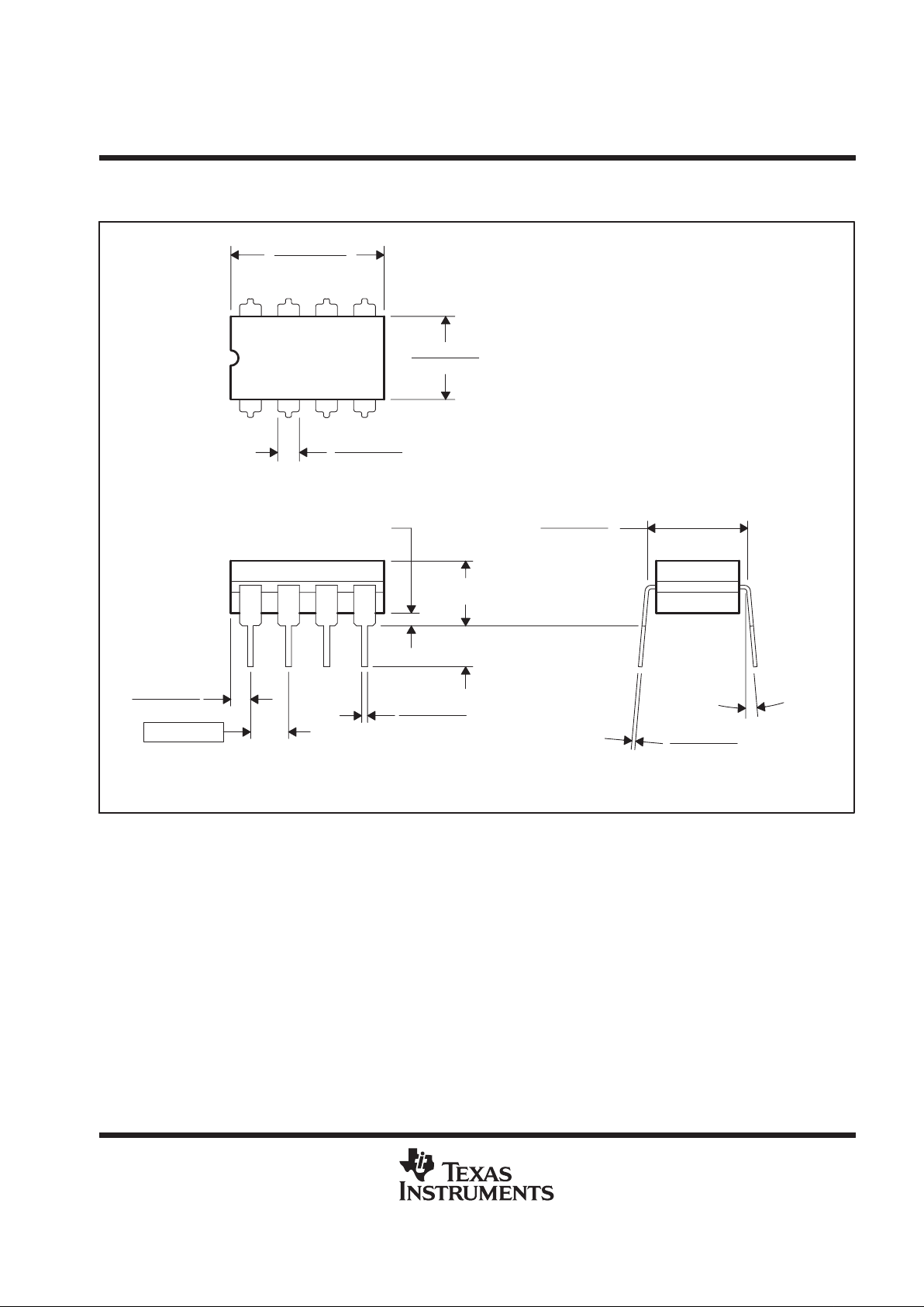
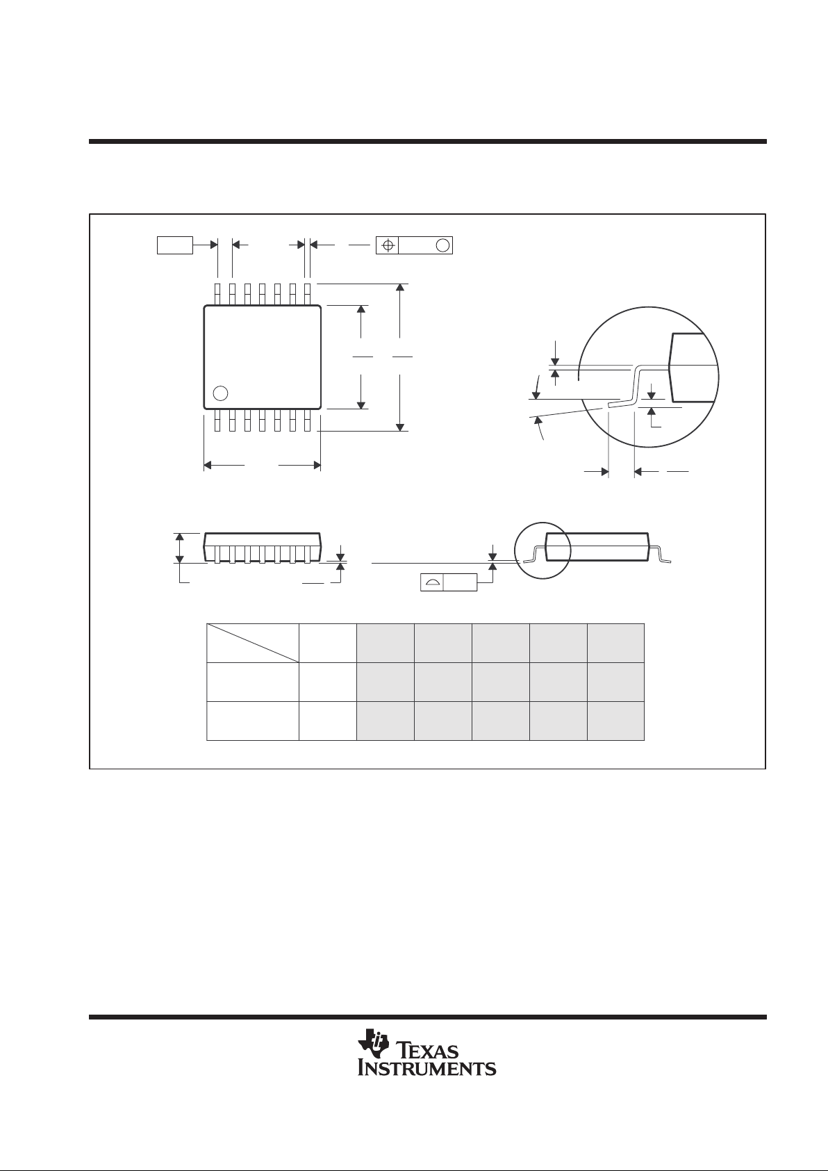
MECHANICAL DATA
D (R-PDSO-G**) PLASTIC SMALL-OUTLINE PACKAGE
14 PIN SHOWN
4040047/D 10/96
0.228 (5,80)
0.244 (6,20)
0.069 (1,75) MAX
0.010 (0,25)
0.004 (0,10)
1
14
0.014 (0,35)
0.020 (0,51)
A
0.157 (4,00)
0.150 (3,81)
7
8
0.044 (1,12)
0.016 (0,40)
Seating Plane
0.010 (0,25)
PINS **
0.008 (0,20) NOM
A MIN
A MAX
DIM
Gage Plane
0.189
(4,80)
(5,00)
0.197
8
(8,55)
(8,75)
0.337
14
0.344
(9,80)
16
0.394
(10,00)
0.386
0.004 (0,10)
M
0.010 (0,25)
0.050 (1,27)
0°–8°
NOTES: A. All linear dimensions are in inches (millimeters).
B. This drawing is subject to change without notice.
C. Body dimensions do not include mold flash or protrusion, not to exceed 0.006 (0,15).
D. Falls within JEDEC MS-012

TLC7701, TLC7725, TLC7703, TLC7733, TLC7705
MICROPOWER SUPPLY VOLTAGE SUPERVISORS
SLVS087K – DECEMBER 1994 – REVISED JULY 1999
14
POST OFFICE BOX 655303 • DALLAS, TEXAS 75265
MECHANICAL DATA
FK (S-CQCC-N**) LEADLESS CERAMIC CHIP CARRIER
4040140/D 10/96
28 TERMINAL SHOWN
B
0.358
(9,09)
MAX
(11,63)
0.560
(14,22)
0.560
0.458
0.858
(21,8)
1.063
(27,0)
(14,22)
A
NO. OF
MINMAX
0.358
0.660
0.761
0.458
0.342
(8,69)
MIN
(11,23)
(16,26)
0.640
0.739
0.442
(9,09)
(11,63)
(16,76)
0.962
1.165
(23,83)
0.938
(28,99)
1.141
(24,43)
(29,59)
(19,32)(18,78)
**
20
28
52
44
68
84
0.020 (0,51)
TERMINALS
0.080 (2,03)
0.064 (1,63)
(7,80)
0.307
(10,31)
0.406
(12,58)
0.495
(12,58)
0.495
(21,6)
0.850
(26,6)
1.047
0.045 (1,14)
0.045 (1,14)
0.035 (0,89)
0.035 (0,89)
0.010 (0,25)
12
1314151618 17
11
10
8
9
7
5
432
0.020 (0,51)
0.010 (0,25)
6
12826 27
19
21
B SQ
A SQ
22
23
24
25
20
0.055 (1,40)
0.045 (1,14)
0.028 (0,71)
0.022 (0,54)
0.050 (1,27)
NOTES: A. All linear dimensions are in inches (millimeters).
B. This drawing is subject to change without notice.
C. This package can be hermetically sealed with a metal lid.
D. The terminals are gold plated.
E. Falls within JEDEC MS-004
TLC7701, TLC7725, TLC7703, TLC7733, TLC7705
MICROPOWER SUPPLY VOLTAGE SUPERVISORS
SLVS087K – DECEMBER 1994 – REVISED JULY 1999
15
POST OFFICE BOX 655303 • DALLAS, TEXAS 75265
MECHANICAL DATA
JG (R-GDIP-T8) CERAMIC DUAL-IN-LINE PACKAGE
0.310 (7,87)
0.290 (7,37)
0.014 (0,36)
0.008 (0,20)
Seating Plane
4040107/C 08/96
5
4
0.065 (1,65)
0.045 (1,14)
8
1
0.020 (0,51) MIN
0.400 (10,20)
0.355 (9,00)
0.015 (0,38)
0.023 (0,58)
0.063 (1,60)
0.015 (0,38)
0.200 (5,08) MAX
0.130 (3,30) MIN
0.245 (6,22)
0.280 (7,11)
0.100 (2,54)
0°–15°
NOTES: A. All linear dimensions are in inches (millimeters).
B. This drawing is subject to change without notice.
C. This package can be hermetically sealed with a ceramic lid using glass frit.
D. Index point is provided on cap for terminal identification only on press ceramic glass frit seal only.
E. Falls within MIL-STD-1835 GDIP1-T8
TLC7701, TLC7725, TLC7703, TLC7733, TLC7705
MICROPOWER SUPPLY VOLTAGE SUPERVISORS
SLVS087K – DECEMBER 1994 – REVISED JULY 1999
16
POST OFFICE BOX 655303 • DALLAS, TEXAS 75265
MECHANICAL DATA
P (R-PDIP-T8) PLASTIC DUAL-IN-LINE PACKAGE
4040082/B 03/95
0.310 (7,87)
0.290 (7,37)
0.010 (0,25) NOM
0.400 (10,60)
0.355 (9,02)
58
41
0.020 (0,51) MIN
0.070 (1,78) MAX
0.240 (6,10)
0.260 (6,60)
0.200 (5,08) MAX
0.125 (3,18) MIN
0.015 (0,38)
0.021 (0,53)
Seating Plane
M
0.010 (0,25)
0.100 (2,54)
0°–15°
NOTES: A. All linear dimensions are in inches (millimeters).
B. This drawing is subject to change without notice.
C. Falls within JEDEC MS-001
TLC7701, TLC7725, TLC7703, TLC7733, TLC7705
MICROPOWER SUPPLY VOLTAGE SUPERVISORS
SLVS087K – DECEMBER 1994 – REVISED JULY 1999
17
POST OFFICE BOX 655303 • DALLAS, TEXAS 75265
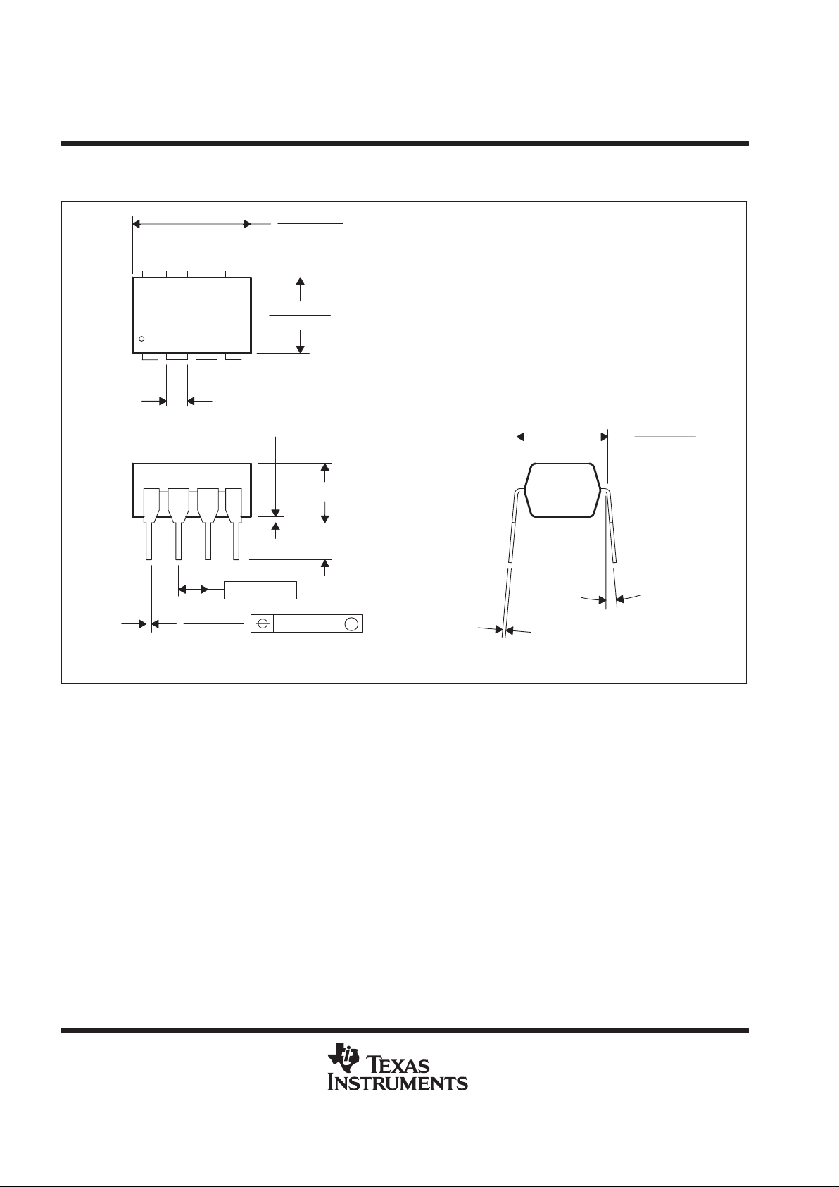
MECHANICAL DATA
PW (R-PDSO-G**) PLASTIC SMALL-OUTLINE PACKAGE
4040064/E 08/96
14 PIN SHOWN
Seating Plane
1,20 MAX
1
A
7
14
0,19
4,50
4,30
8
6,20
6,60
0,30
0,75
0,50
0,25
Gage Plane
0,15 NOM
0,65
M
0,10
0°–8°
0,10
PINS **
A MIN
A MAX
DIM
2,90
3,10
8
4,90
5,10
14
6,60
6,404,90
5,10
16
7,70
20
7,90
24
9,60
9,80
28
0,15
0,05
NOTES: A. All linear dimensions are in millimeters.
B. This drawing is subject to change without notice.
C. Body dimensions do not include mold flash or protrusion not to exceed 0,15.
D. Falls within JEDEC MO-153
TLC7701, TLC7725, TLC7703, TLC7733, TLC7705
MICROPOWER SUPPLY VOLTAGE SUPERVISORS
SLVS087K – DECEMBER 1994 – REVISED JULY 1999
18
POST OFFICE BOX 655303 • DALLAS, TEXAS 75265
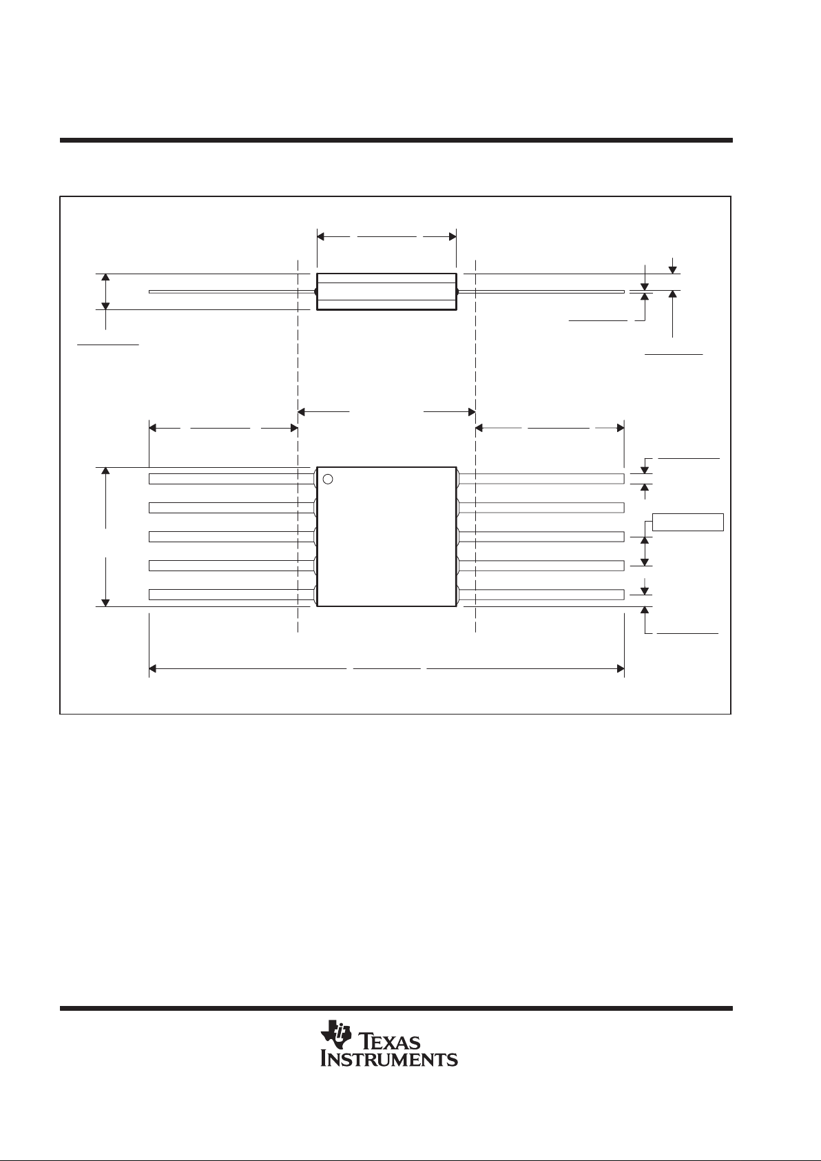
MECHANICAL DATA
U (S-GDFP-F10) CERAMIC DUAL FLATPACK
4040179/B 03/95
1.000 (25,40)
0.080 (2,03)
0.250 (6,35)
0.250 (6,35)
0.019 (0,48)
0.025 (0,64)
0.300 (7,62)
0.045 (1,14)
0.006 (0,15)
0.050 (1,27)
0.015 (0,38)
0.005 (0,13)
0.026 (0,66)
0.004 (0,10)
0.246 (6,10)
0.750 (19,05)
1
10
5
6
0.250 (6,35)
0.350 (8,89)0.350 (8,89)
0.250 (6,35)
0.050 (1,27)
NOTES: A. All linear dimensions are in inches (millimeters).
B. This drawing is subject to change without notice.
C. This package can be hermetically sealed with a ceramic lid using glass frit.
D. Index point is provided on cap for terminal identification only.
E. Falls within MIL STD 1835 GDFP1-F10 and JEDEC MO-092AA

IMPORTANT NOTICE
T exas Instruments and its subsidiaries (TI) reserve the right to make changes to their products or to discontinue
any product or service without notice, and advise customers to obtain the latest version of relevant information
to verify, before placing orders, that information being relied on is current and complete. All products are sold
subject to the terms and conditions of sale supplied at the time of order acknowledgement, including those
pertaining to warranty, patent infringement, and limitation of liability.
TI warrants performance of its semiconductor products to the specifications applicable at the time of sale in
accordance with TI’s standard warranty. Testing and other quality control techniques are utilized to the extent
TI deems necessary to support this warranty. Specific testing of all parameters of each device is not necessarily
performed, except those mandated by government requirements.
CERT AIN APPLICATIONS USING SEMICONDUCTOR PRODUCTS MAY INVOLVE POTENTIAL RISKS OF
DEATH, PERSONAL INJURY, OR SEVERE PROPERTY OR ENVIRONMENTAL DAMAGE (“CRITICAL
APPLICATIONS”). TI SEMICONDUCTOR PRODUCTS ARE NOT DESIGNED, AUTHORIZED, OR
WARRANTED TO BE SUITABLE FOR USE IN LIFE-SUPPORT DEVICES OR SYSTEMS OR OTHER
CRITICAL APPLICATIONS. INCLUSION OF TI PRODUCTS IN SUCH APPLICA TIONS IS UNDERSTOOD T O
BE FULLY AT THE CUSTOMER’S RISK.
In order to minimize risks associated with the customer’s applications, adequate design and operating
safeguards must be provided by the customer to minimize inherent or procedural hazards.
TI assumes no liability for applications assistance or customer product design. TI does not warrant or represent
that any license, either express or implied, is granted under any patent right, copyright, mask work right, or other
intellectual property right of TI covering or relating to any combination, machine, or process in which such
semiconductor products or services might be or are used. TI’s publication of information regarding any third
party’s products or services does not constitute TI’s approval, warranty or endorsement thereof.
Copyright 1999, Texas Instruments Incorporated
 Loading...