Texas Instruments TLC7628IN, TLC7628CN, TLC7628CDWR, TLC7628CDW Datasheet

TLC7628C, TLC7628E, TLC7628I
DUAL 8-BIT MULTIPLYING
DIGITAL-TO-ANALOG CONVERTERS
SLAS063A – APRIL 1989 – REVISED MA Y 1995
1
POST OFFICE BOX 655303 • DALLAS, TEXAS 75265
D
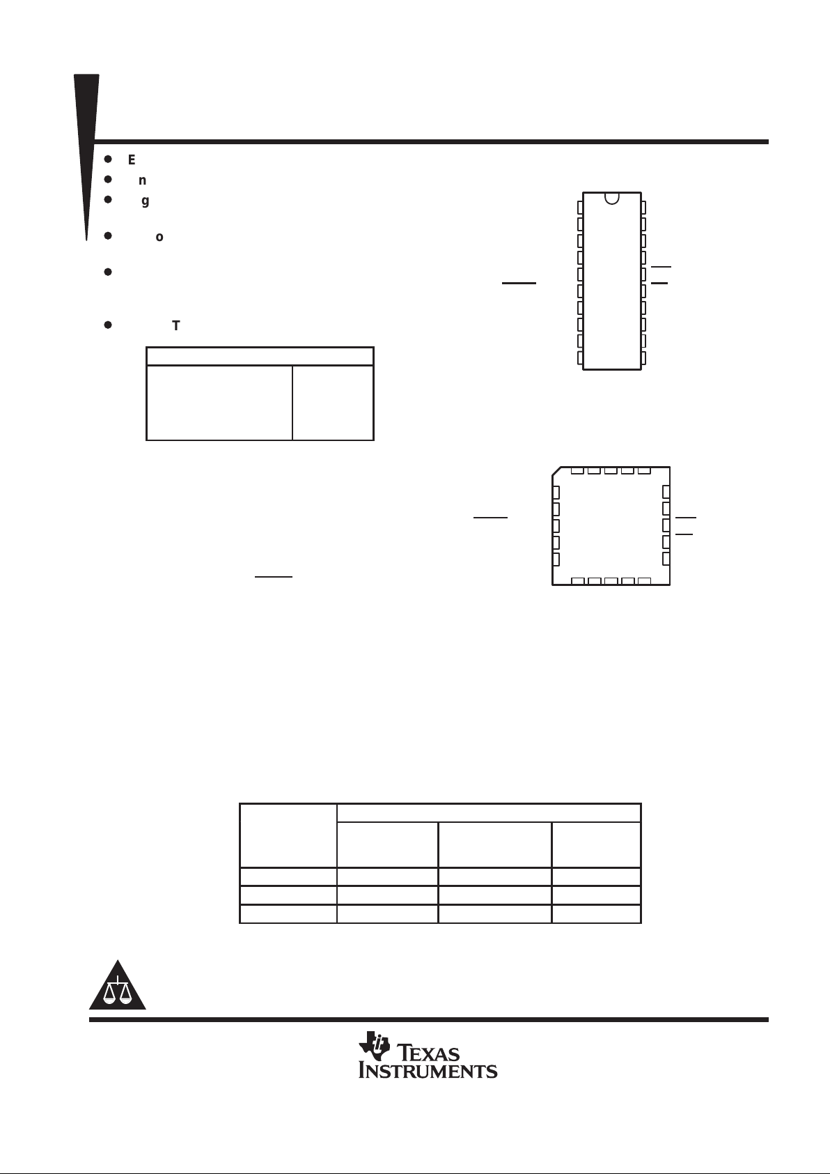
Easy Microprocessor Interface
D
On-Chip Data Latches
D
Digital Inputs Are TTL-Compatible With
10.8-V to 15.75-V Power Supply
D
Monotonic Over the Entire A/D Conversion
Range
D
Fast Control Signaling for Digital Signal
Processor (DSP) Applications Including
Interface With TMS320
D
CMOS Technology
KEY PERFORMANCE SPECIFICATIONS
Resolution
Linearity Error
Power Dissipation
Settling Time
Propagation Delay Time
8 bits
1/2 LSB
20 mW
100 ns
80 ns
description
The TLC7628C, TLC7628E, and TLC7628I are
dual, 8-bit, digital-to-analog converters (DACs)
designed with separate on-chip data latches and
feature exceptionally close DAC-to-DAC
matching. Data is transferred to either of the two
DAC data latches through a common, 8-bit input
port. Control input DACA
/DACB determines
which DAC is loaded. The load cycle of these
devices is similar to the write cycle of a
random-access memory, allowing easy interface
to most popular microprocessor buses and output ports. Segmenting the high-order bits minimizes glitches
during changes in the most significant bits, where glitch impulse is typically the strongest.
The TLC7628C operates from a 10.8-V to 15.75-V power supply and is TTL-compatible over this range. 2- or
4-quadrant multiplying makes these devices a sound choice for many microprocessor-controlled gain-setting
and signal-control applications.
The TLC7628C is characterized for operation from 0°C to 70°C. The TLC7628I is characterized for operation
from –25°C to 85°C. The TLC7628E is characterized for operation from –40°C to 85°C.
AVAILABLE OPTIONS
PACKAGE
T
A
SMALL OUTLINE
PLASTIC DIP
(DW)
PLASTIC CHIP
CARRIER
(FN)
PLASTIC DIP
(N)
0°C to 70°C TLC7628CDW TLC7628CFN TLC7628CN
–25°C to 85°C TLC7628IDW TLC7628IFN TLC7628IN
–40°C to 85°C TLC7628EDW TLC7628EFN TLC7628EN
Copyright 1995, Texas Instruments Incorporated
PRODUCTION DATA information is current as of publication date.
Products conform to specifications per the terms of Texas Instruments
standard warranty. Production processing does not necessarily include
testing of all parameters.
Please be aware that an important notice concerning availability, standard warranty, and use in critical applications of
Texas Instruments semiconductor products and disclaimers thereto appears at the end of this data sheet.
1
2
3
4
5
6
7
8
9
10
20
19
18
17
16
15
14
13
12
11
AGND
OUTA
RFBA
REFA
DGND
DACA
/DACB
(MSB) DB7
DB6
DB5
DB4
OUTB
RFBB
REFB
V
DD
WR
CS
DB0 (LSB)
DB1
DB2
DB3
DW OR N PACKAGE
(TOP VIEW)
3212019
910111213
4
5
6
7
8
18
17
16
15
14
REFB
V
DD
WR
CS
DB0 (LSB)
REFA
DGND
DACA
/DACB
(MSB) DB7
DB6
FN PACKAGE
(TOP VIEW)
RFBA
OUTA
AGND
DB2
DB1
OUTB
RFBB
DB5
DB4
DB3

TLC7628C, TLC7628E, TLC7628I
DUAL 8-BIT MULTIPLYING
DIGITAL-TO-ANALOG CONVERTERS
SLAS063A – APRIL 1989 – REVISED MA Y 1995
2
POST OFFICE BOX 655303 • DALLAS, TEXAS 75265
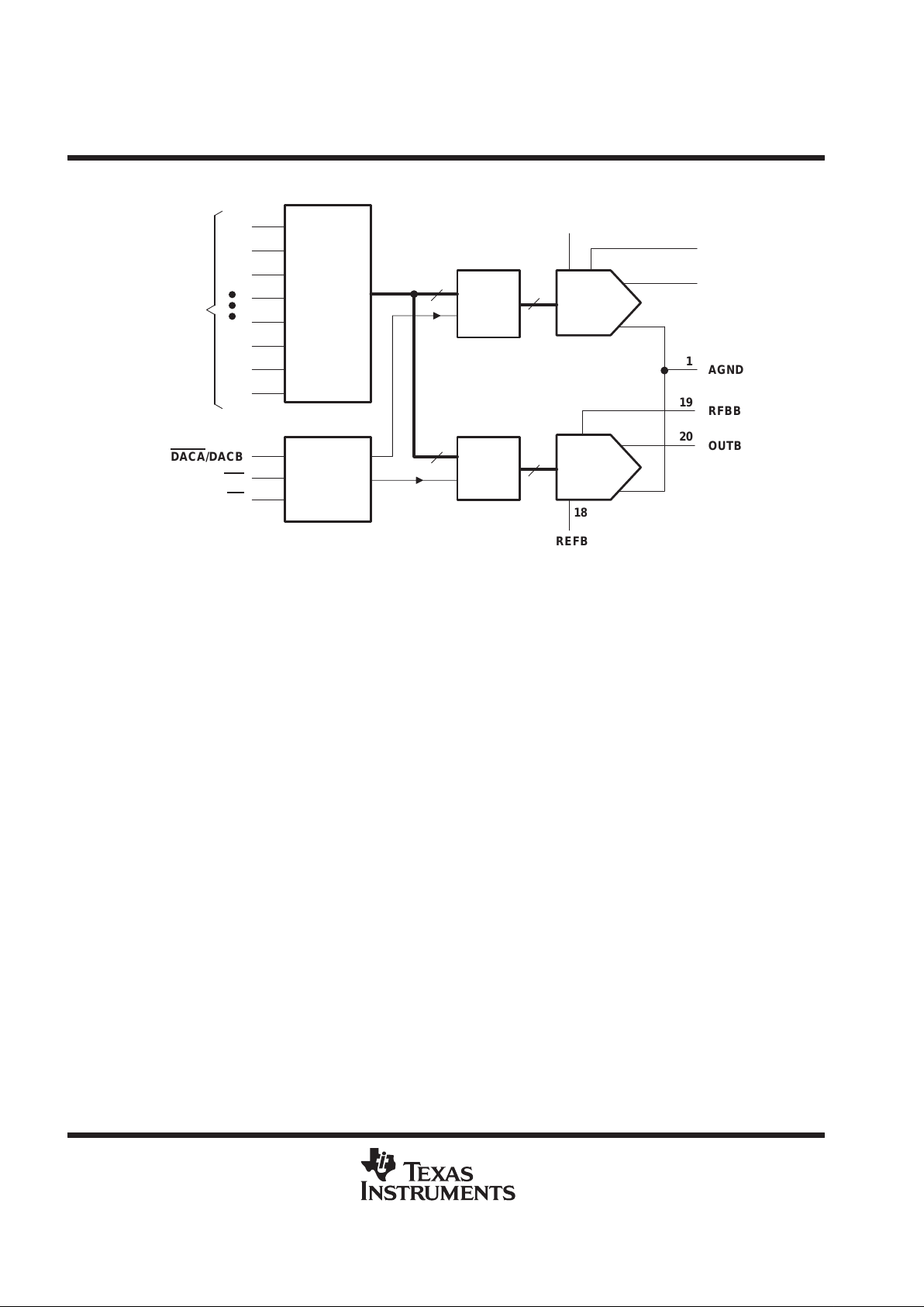
functional block diagram
DACA/DACB
REFB
18
OUTB
20
RFBB
19
AGND
1
OUTA
2
RFBA
3
REFA
4
DACA
Input
Buffer
Logic
Control
DACB
DB0
DB7
CS
WR
15
16
6
Data
Inputs
7
8
9
10
11
12
13
14
8
8
8
8
Latch A
Latch B
absolute maximum ratings over operating free-air temperature range (unless otherwise noted)
†
Supply voltage range, V
DD
(to AGND or DGND) –0.3 V to 17 V. . . . . . . . . . . . . . . . . . . . . . . . . . . . . . . . . . . . . .
Voltage between AGND and DGND V
DD
. . . . . . . . . . . . . . . . . . . . . . . . . . . . . . . . . . . . . . . . . . . . . . . . . . . . . . . . . .
Input voltage range, V
I
(to DGND) –0.3 V to V
DD
+ 0.3 V. . . . . . . . . . . . . . . . . . . . . . . . . . . . . . . . . . . . . . . . . . . .
Reference voltage range, V
refA
or V
refB
(to AGND) ±25 V. . . . . . . . . . . . . . . . . . . . . . . . . . . . . . . . . . . . . . . . . .
Feedback voltage range, V
RFBA
or V
RFBB
(to AGND) ±25 V. . . . . . . . . . . . . . . . . . . . . . . . . . . . . . . . . . . . . . .
Output voltage range, V
OA
or VOB (to AGND) ±25 V. . . . . . . . . . . . . . . . . . . . . . . . . . . . . . . . . . . . . . . . . . . . . . .
Peak input current 10 µA. . . . . . . . . . . . . . . . . . . . . . . . . . . . . . . . . . . . . . . . . . . . . . . . . . . . . . . . . . . . . . . . . . . . . . .
Operating free-air temperature range, T
A
: TLC7628C 0°C to 70°C. . . . . . . . . . . . . . . . . . . . . . . . . . . . . . . . . .
TLC7628I –25°C to 85°C. . . . . . . . . . . . . . . . . . . . . . . . . . . . . . . . .
TLC7628E –40°C to 85°C. . . . . . . . . . . . . . . . . . . . . . . . . . . . . . . .
Storage temperature range, T
stg
–65°C to 150°C. . . . . . . . . . . . . . . . . . . . . . . . . . . . . . . . . . . . . . . . . . . . . . . . . . .
Case temperature for 10 seconds, T
C
: FN package 260°C. . . . . . . . . . . . . . . . . . . . . . . . . . . . . . . . . . . . . . . . . .
Lead temperature 1,6 mm (1/16 inch) from case for 10 seconds: DW or N package 260°C. . . . . . . . . . . . . .
†
Stresses beyond those listed under “absolute maximum ratings” may cause permanent damage to the device. These are stress ratings only, and
functional operation of the device at these or any other conditions beyond those indicated under “recommended operating conditions” is not
implied. Exposure to absolute-maximum-rated conditions for extended periods may affect device reliability.

TLC7628C, TLC7628E, TLC7628I
DUAL 8-BIT MULTIPLYING
DIGITAL-TO-ANALOG CONVERTERS
SLAS063A – APRIL 1989 – REVISED MA Y 1995
3
POST OFFICE BOX 655303 • DALLAS, TEXAS 75265
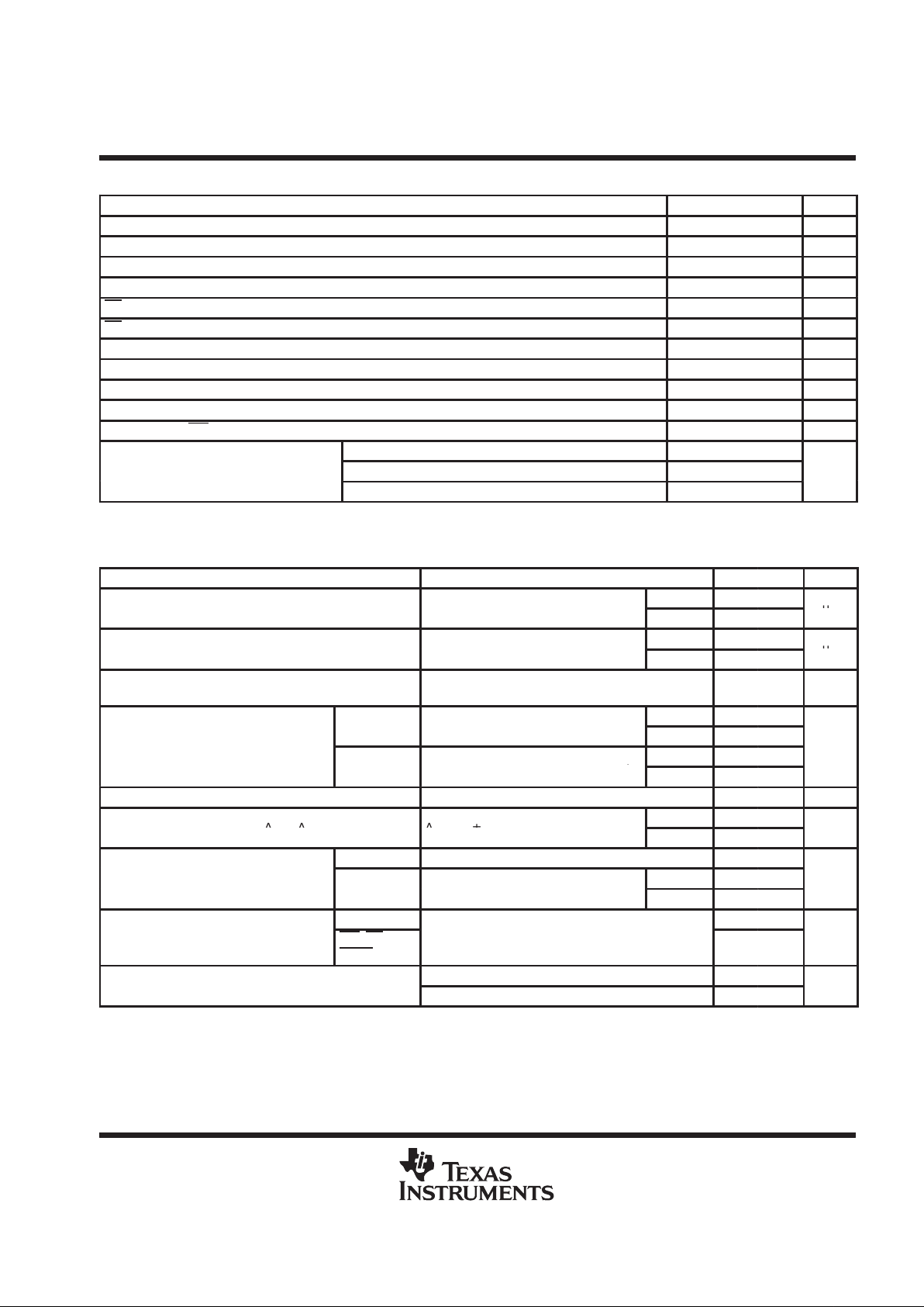
recommended operating conditions
MIN NOM MAX UNIT
Supply voltage, V
DD
10.8 15.75 V
Reference voltage, V
refA
or V
refB
±10 V
High-level input voltage, V
IH
2.4 V
Low-level input voltage, V
IL
0.8 V
CS setup time, t
su(CS)
50 ns
CS hold time, t
h(CS)
(see Figure 1) 0 ns
DAC select setup time, t
su(DAC)
(see Figure 1) 60 ns
DAC select hold time, t
h(DAC)
(see Figure 1) 10 ns
Data bus input setup time t
su(D)
(see Figure 1) 25 ns
Data bus input hold time t
h(D)
(see Figure 1) 10 ns
Pulse duration, WR low, t
w(WR)
(see Figure 1) 50 ns
TLC7628C 0 70
Operating free-air temperature, T
A
TLC7628I –25 85
°C
TLC7628E –40 85
electrical characteristics over recommended ranges of operating free-air temperature and VDD,
V
refA
= V
refB
= 10 V, VOA and VOB at 0 V (unless otherwise noted)
PARAMETER TEST CONDITIONS MIN MAX UNIT
p
Full range 10
IIHHigh-level input current
V
I
=
V
DD
25°C 1
µ
A
p
Full range –10
IILLow-level input current
V
I
=
0
25°C –1
µ
A
Reference input impedance REFA or REFB to
AGND
5 20 kΩ
DAC data latch loaded with 00000000,
Full range ±200
p
OUTA
,
V
refA
= ±10 V
25°C ±50
IkgOutput leakage current
DAC data latch loaded with 00000000,
Full range ±200
nA
OUTB
,
V
refB
= ±10 V
25°C ±50
Input resistance match (REFA to REFB) ±1%
pp
Full range 0.02
DC supply sensitivity ∆gain/∆V
DD
∆V
DD
=
± 5 %
25°C 0.01
%/%
Quiescent All digital inputs at VIHmin or VILmax 2
I
DD
Supply current
p
Full range 0.5
mA
Standb
y
All digital inputs at 0 V or V
DD
25°C 0.1
DB0–DB7 10
C
i
Input capacitance
WR
, CS,
DACA
/DACB
15
pF
p
p
DAC data latches loaded with 00000000 25
p
CoOutput capacitance (OUTA, OUTB)
DAC data latches loaded with 11111111 60
pF
 Loading...