TLC7528C, TLC7528E, TLC7528I
DUAL 8-BIT MULTIPLYING
DIGITAL-TO-ANALOG CONVERTERS
SLAS062B – JANUARY 1987 – REVISED MARCH 2000
1
POST OFFICE BOX 655303 • DALLAS, TEXAS 75265
D
Easily Interfaced to Microprocessors
D
On-Chip Data Latches
D
Monotonic Over the Entire A/D Conversion
Range
D
Interchangeable With Analog Devices
AD7528 and PMI PM-7528
D
Fast Control Signaling for Digital Signal
Processor (DSP) Applications Including
Interface With TMS320
D
Voltage-Mode Operation
D
CMOS T echnology
KEY PERFORMANCE SPECIFICATIONS
Resolution
Linearity Error
Power Dissipation at VDD = 5 V
Settling Time at VDD = 5 V
Propagation Delay Time at VDD = 5 V
8 bits
1/2 LSB
20 mW
100 ns
80 ns
description
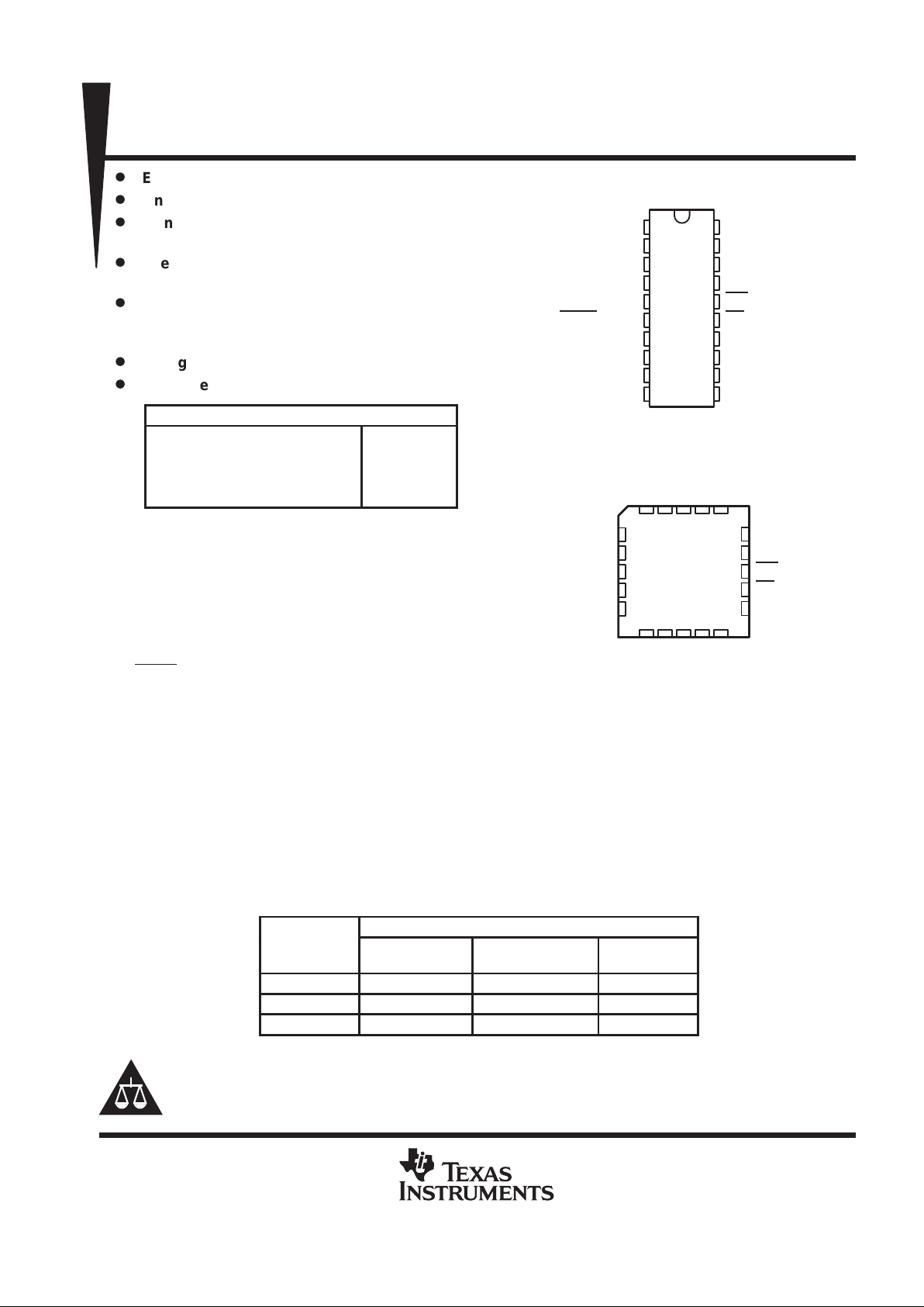
The TLC7528C, TLC7528E, and TLC7528I are
dual, 8-bit, digital-to-analog converters designed
with separate on-chip data latches and feature
exceptionally close DAC-to-DAC matching. Data
is transferred to either of the two DAC data latches
through a common, 8-bit, input port. Control input
DACA
/DACB determines which DAC is to be
loaded. The load cycle of these devices is similar
to the write cycle of a random-access memory , allowing easy interface to most popular microprocessor buses
and output ports. Segmenting the high-order bits minimizes glitches during changes in the most significant bits,
where glitch impulse is typically the strongest.
These devices operate from a 5-V to 15-V power supply and dissipates less than 15 mW (typical). The 2- or
4-quadrant multiplying makes these devices a sound choice for many microprocessor-controlled gain-setting
and signal-control applications. It can be operated in voltage mode, which produces a voltage output rather than
a current output. Refer to the typical application information in this data sheet.
The TLC7528C is characterized for operation from 0°C to 70°C. The TLC7528I is characterized for operation
from –25°C to 85°C. The TLC7528E is characterized for operation from –40°C to 85°C.
AVAILABLE OPTIONS
PACKAGE
T
A
SMALL OUTLINE
(DW)
CHIP CARRIER
(FN)
PLASTIC DIP
(N)
0°C to 70°C TLC7528CDW TLC7528CFN TLC7528CN
–25°C to 85°C TLC7528IDW TLC7528IFN TLC7528IN
–40°C to 85°C TLC7528EDW TLC7528EFN TLC7528EN
Copyright 2000, Texas Instruments Incorporated
PRODUCTION DATA information is current as of publication date.
Products conform to specifications per the terms of Texas Instruments
standard warranty. Production processing does not necessarily include
testing of all parameters.
Please be aware that an important notice concerning availability, standard warranty, and use in critical applications of
Texas Instruments semiconductor products and disclaimers thereto appears at the end of this data sheet.
1
2
3
4
5
6
7
8
9
10
20
19
18
17
16
15
14
13
12
11
AGND
OUTA
RFBA
REFA
DGND
DACA
/DACB
(MSB) DB7
DB6
DB5
DB4
OUTB
RFBB
REFB
V
DD
WR
CS
DB0 (LSB)
DB1
DB2
DB3
DW OR N PACKAGE
(TOP VIEW)
3212019
910111213
4
5
6
7
8
18
17
16
15
14
REFB
V
DD
WR
CS
DB0 (LSB)
REFA
DGND
DACA/DACB
(MSB) DB7
DB6
FN PACKAGE
(TOP VIEW)
RFBA
OUTA
AGND
DB2
DB1
OUTB
RFBB
DB5
DB4
DB3
TLC7528C, TLC7528E, TLC7528I
DUAL 8-BIT MULTIPLYING
DIGITAL-TO-ANALOG CONVERTERS
SLAS062B – JANUARY 1987 – REVISED MARCH 2000
2
POST OFFICE BOX 655303 • DALLAS, TEXAS 75265
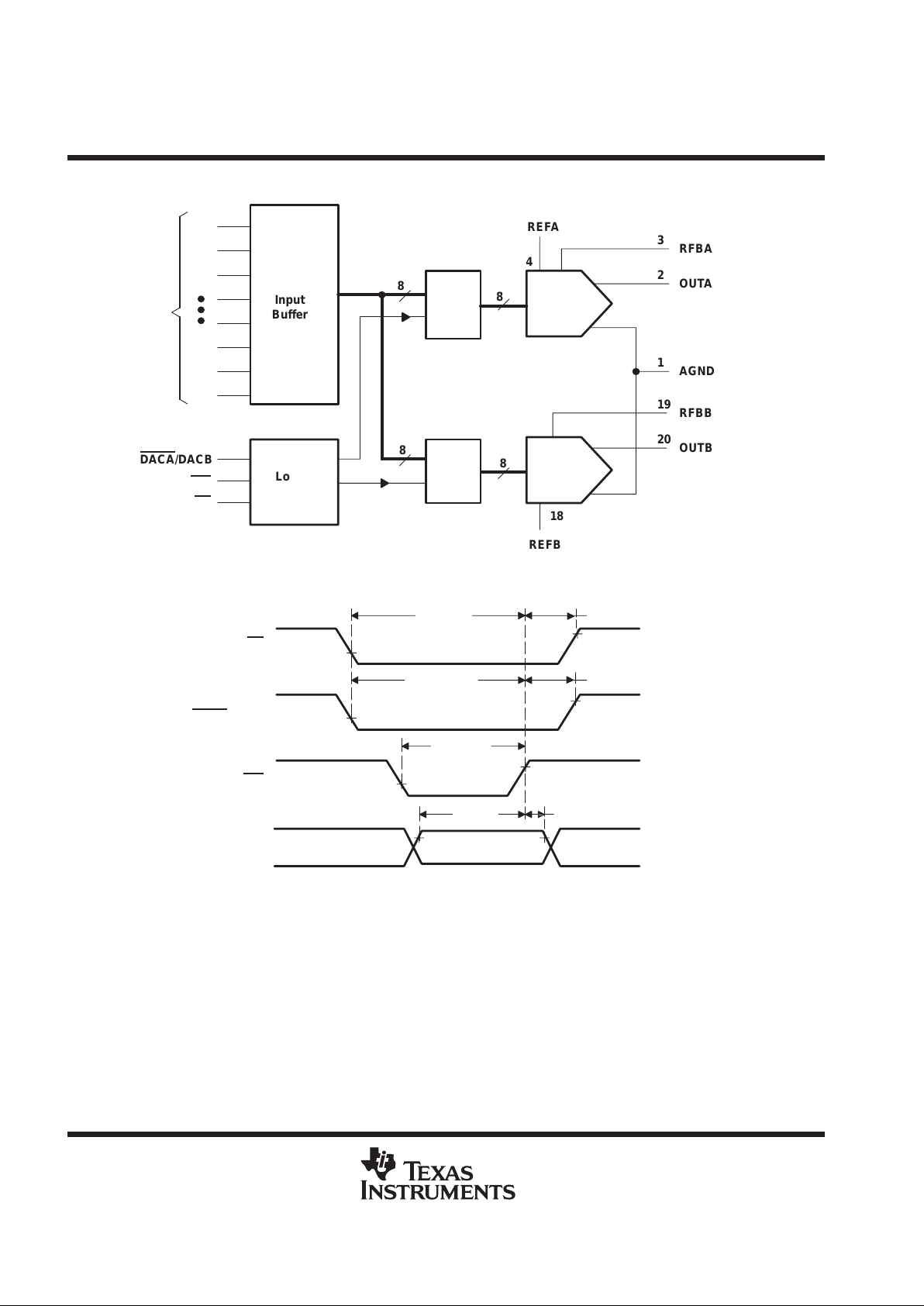
functional block diagram
8
8
8
8
DACA
/DACB
REFB
18
OUTB
20
RFBB
19
AGND
1
OUTA
2
RFBA
3
REFA
4
Input
Buffer
Logic
Control
DB0
DB7
CS
WR
15
16
6
Data
Inputs
7
8
9
10
11
12
13
14
DACA
DACB
Latch B
Latch A
operating sequence
t
h(DAC)
t
h(CS)
t
su(CS)
t
su(DAC
)
t
w(WR)
t
h(D)
t
su(D)
Data In Stable
DB0–DB7
WR
CS
DACA/DACB
TLC7528C, TLC7528E, TLC7528I
DUAL 8-BIT MULTIPLYING
DIGITAL-TO-ANALOG CONVERTERS
SLAS062B – JANUARY 1987 – REVISED MARCH 2000
3
POST OFFICE BOX 655303 • DALLAS, TEXAS 75265
absolute maximum ratings over operating free-air temperature range (unless otherwise noted)
†
Supply voltage range, VDD (to AGND or DGND) –0.3 V to 16.5 V. . . . . . . . . . . . . . . . . . . . . . . . . . . . . . . . . . . .
Voltage between AGND and DGND ±V
DD
. . . . . . . . . . . . . . . . . . . . . . . . . . . . . . . . . . . . . . . . . . . . . . . . . . . . . . . . .
Input voltage range, VI (to DGND) –0.3 V to VDD + 0.3. . . . . . . . . . . . . . . . . . . . . . . . . . . . . . . . . . . . . . . . . . . . . .
Reference voltage, V
refA
or V
refB
(to AGND) ±25 V. . . . . . . . . . . . . . . . . . . . . . . . . . . . . . . . . . . . . . . . . . . . . . . . .
Feedback voltage V
RFBA
or V
RFBB
(to AGND) ±25 V. . . . . . . . . . . . . . . . . . . . . . . . . . . . . . . . . . . . . . . . . . . . . . .
Input voltage (voltage mode out A, out B to AGND) –0.3 V to VDD + 0.3. . . . . . . . . . . . . . . . . . . . . . . . . . . . . . .
Output voltage, VOA or VOB (to AGND) ±25 V. . . . . . . . . . . . . . . . . . . . . . . . . . . . . . . . . . . . . . . . . . . . . . . . . . . . . .
Peak input current 10 µA. . . . . . . . . . . . . . . . . . . . . . . . . . . . . . . . . . . . . . . . . . . . . . . . . . . . . . . . . . . . . . . . . . . . . . . .
Operating free-air temperature range, TA: TLC7528C 0°C to 70°C. . . . . . . . . . . . . . . . . . . . . . . . . . . . . . . . . . .
TLC7528I –25°C to 85°C. . . . . . . . . . . . . . . . . . . . . . . . . . . . . . . .
TLC7528E –40°C to 85°C. . . . . . . . . . . . . . . . . . . . . . . . . . . . . . . .
Storage temperature range, T
stg
–65°C to 150°C. . . . . . . . . . . . . . . . . . . . . . . . . . . . . . . . . . . . . . . . . . . . . . . . . .
Case temperature for 10 seconds, TC: FN package 260°C. . . . . . . . . . . . . . . . . . . . . . . . . . . . . . . . . . . . . . . . . .
Lead temperature 1,6 mm (1/16 inch) from case for 10 seconds: DW or N package 260°C. . . . . . . . . . . . . . .
†
Stresses beyond those listed under “absolute maximum ratings” may cause permanent damage to the device. These are stress ratings only, and
functional operation of the device at these or any other conditions beyond those indicated under “recommended operating conditions” is not
implied. Exposure to absolute-maximum-rated conditions for extended periods may affect device reliability.
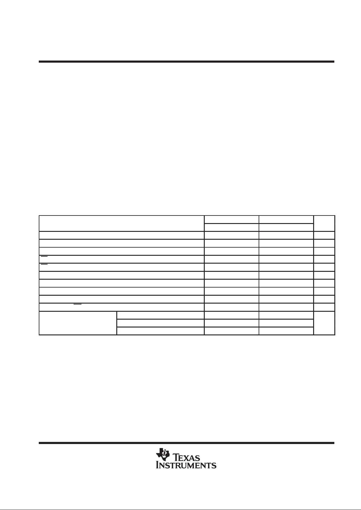
recommended operating conditions
VDD = 4.75 V to 5.25 V VDD = 14.5 V to 15.5 V
MIN NOM MAX MIN NOM MAX
UNIT
Reference voltage, V
refA
or V
refB
±10 ±10 V
High-level input voltage, V
IH
2.4 13.5 V
Low-level input voltage, V
IL
0.8 1.5 V
CS setup time, t
su(CS)
50 50 ns
CS hold time, t
h(CS)
0 0 ns
DAC select setup time, t
su(DAC)
50 50 ns
DAC select hold time, t
h(DAC)
10 10 ns
Data bus input setup time t
su(D)
25 25 ns
Data bus input hold time t
h(D)
10 10 ns
Pulse duration, WR low, t
w(WR)
50 50 ns
TLC7628C 0 70 0 70
Operating free-air temperature, T
A
TLC7628I –25 85 –25 85
°C
TLC7628E –40 85 –40 85
TLC7528C, TLC7528E, TLC7528I
DUAL 8-BIT MULTIPLYING
DIGITAL-TO-ANALOG CONVERTERS
SLAS062B – JANUARY 1987 – REVISED MARCH 2000
4
POST OFFICE BOX 655303 • DALLAS, TEXAS 75265
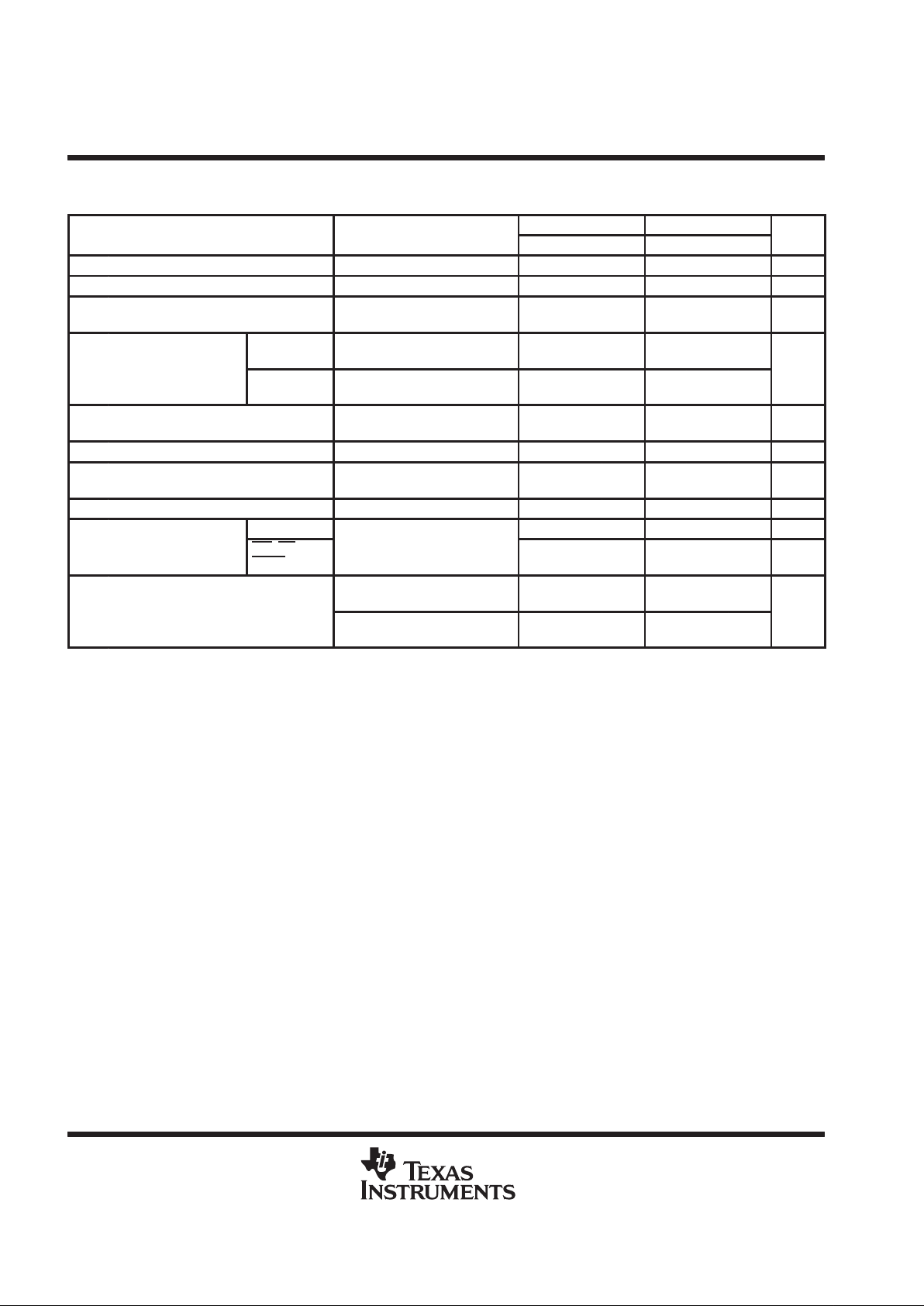
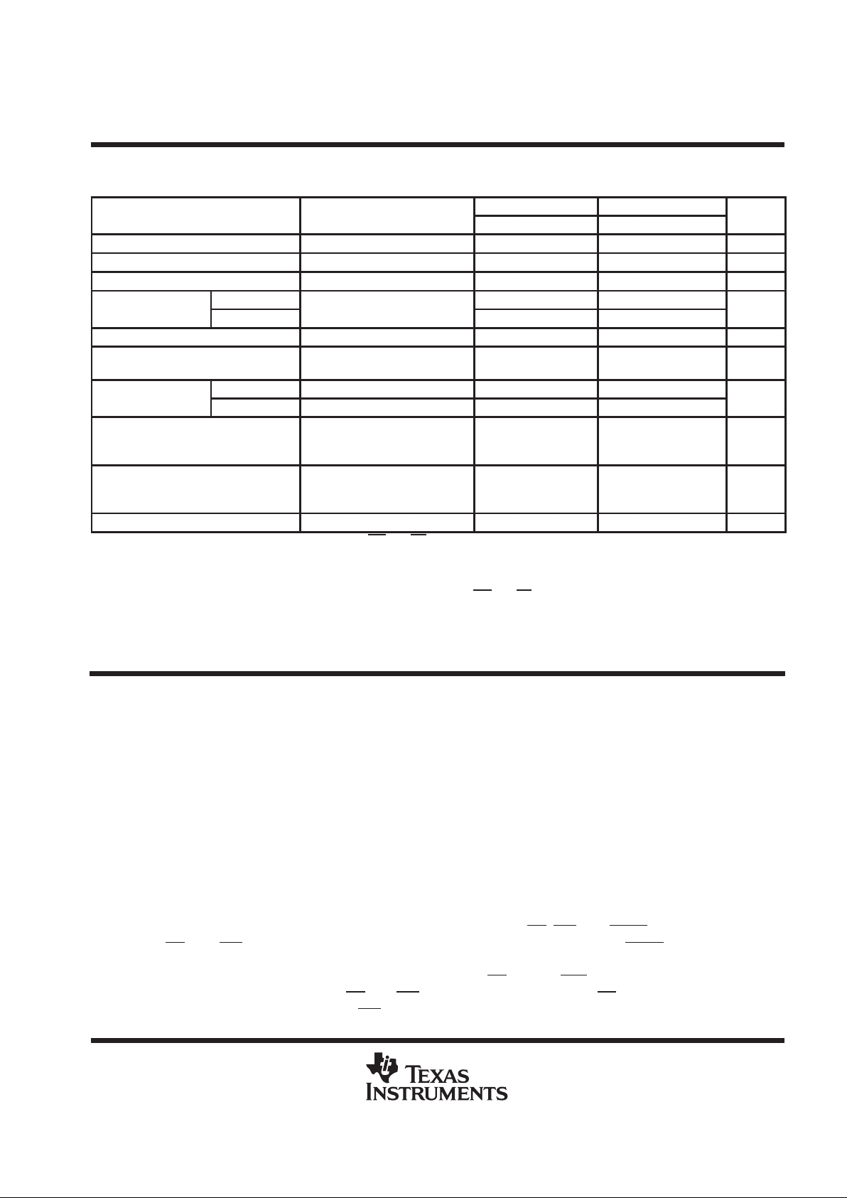
electrical characteristics over recommended operating free-air temperature range,
V
refA
= V
refB
= 10 V, VOA and VOB at 0 V (unless otherwise noted)
VDD = 5 V VDD = 15 V
PARAMETER
TEST CONDITIONS
MIN TYP†MAX MIN TYP†MAX
UNIT
I
IH
High-level input current VI = V
DD
10 10 µA
I
IL
Low-level input current VI = 0 5 12 –10 5 12 –10 µA
Reference input impedance
REFA or REFB to AGND
20 20 kΩ
p
OUTA
DAC data latch loaded with
00000000, V
refA
= ±10 V
±400 ±200
I
Ikg
Output leakage current
OUTB
DAC data latch loaded with
00000000, V
refB
= ±10 V
±400 ±200
nA
Input resistance match
(REFA to REFB)
±1% ±1%
DC supply sensitivity, ∆gain/∆V
DD
∆VDD = ±10% 0.04 0.02 %/%
I
DD
Supply current (quiescent)
All digital inputs at VIHmin or
VILmax
2 2 mA
I
DD
Supply current (standby) All digital inputs at 0 V or V
DD
0.5 0.5 mA
DB0–DB7 10 10 pF
C
i
Input capacitance
WR
, CS,
DACA
/DACB
15 15 pF
p
p
DAC data latches loaded with
00000000
50 50
p
CoOutput capacitance (OUTA, OUTB)
DAC data latches loaded with
11111111
120 120
pF
†
All typical values are at TA = 25°C.
TLC7528C, TLC7528E, TLC7528I
DUAL 8-BIT MULTIPLYING
DIGITAL-TO-ANALOG CONVERTERS
SLAS062B – JANUARY 1987 – REVISED MARCH 2000
5
POST OFFICE BOX 655303 • DALLAS, TEXAS 75265
operating characteristics over recommended operating free-air temperature range,
V
refA
= V
refB
= 10 V, VOA and VOB at 0 V (unless otherwise noted)
VDD = 5 V VDD = 15 V
PARAMETER
TEST CONDITIONS
MIN TYP MAX MIN TYP MAX
UNIT
Linearity error ±1/2 ±1/2 LSB
Settling time (to 1/2 LSB) See Note 1 100 100 ns
Gain error See Note 2 2.5 2.5 LSB
REFA to OUTA
–65 –65
AC feedthrough
REFB to OUTB
See Note 3
–65 –65
dB
Temperature coefficient of gain See Note 4 0.007 0.0035 %FSR/°C
Propagation delay (from digital input to
90% of final analog output current)
See Note 5 80 80 ns
Channel-to-channel
REFA to OUTB See Note 6 77 77
isolation
REFB to OUTA See Note 7 77 77
dB
Digital-to-analog glitch impulse area
Measured for code transition
from 00000000 to 11111111,
TA = 25°C
160 440 nV•s
Digital crosstalk
Measured for code transition
from 00000000 to 11111111,
TA = 25°C
30 60 nV•s
Harmonic distortion Vi = 6 V, f = 1 kHz, TA = 25°C –85 –85 dB
NOTES: 1. OUTA, OUTB load = 100 Ω, C
ext
= 13 pF; WR and CS at 0 V; DB0–DB7 at 0 V to VDD or VDD to 0 V.
2. Gain error is measured using an internal feedback resistor. Nominal full scale range (FSR) = V
ref
– 1 LSB.
3. V
ref
= 20 V peak-to-peak, 100-kHz sine wave; DAC data latches loaded with 00000000.
4. Temperature coefficient of gain measured from 0°C to 25°C or from 25°C to 70°C.
5. V
refA
= V
refB
= 10 V; OUTA/OUTB load = 100 Ω, C
ext
= 13 pF; WR
and CS at 0 V; DB0–DB7 at 0 V to VDD or VDD to 0 V.
6. Both DAC latches loaded with 11111111; V
refA
= 20 V peak-to-peak, 100-kHz sine wave; V
refB
= 0; TA = 25°C.
7. Both DAC latches loaded with 11111111; V
refB
= 20 V peak-to-peak, 100-kHz sine wave; V
refA
= 0; TA = 25°C.
PRINCIPLES OF OPERATION
These devices contain two identical, 8-bit-multiplying D/A converters, DACA and DACB. Each DAC consists
of an inverted R-2R ladder, analog switches, and input data latches. Binary-weighted currents are switched
between DAC output and AGND, thus maintaining a constant current in each ladder leg independent of the
switch state. Most applications require only the addition of an external operational amplifier and voltage
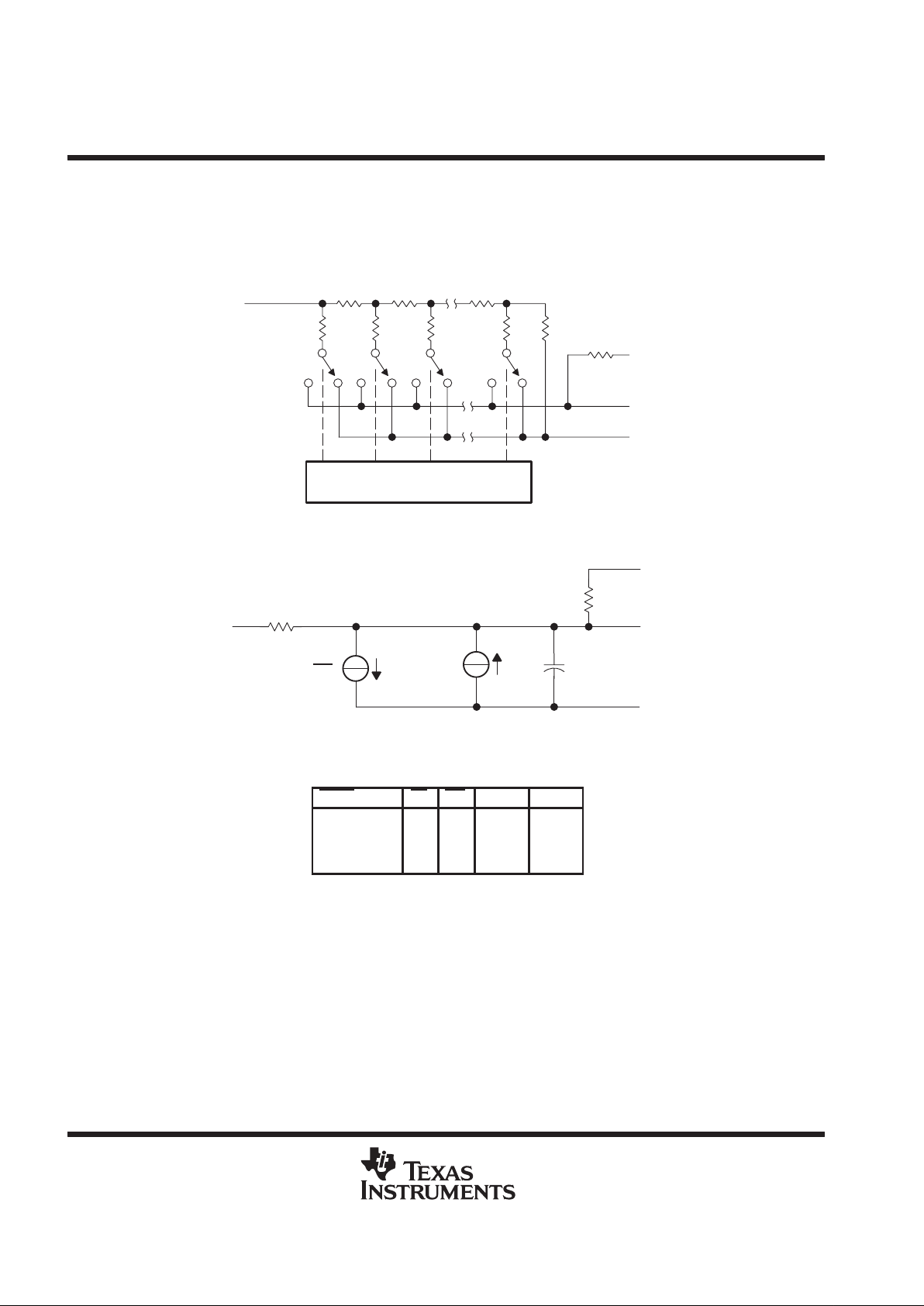
reference. A simplified D/A circuit for DACA with all digital inputs low is shown in Figure 1.
Figure 2 shows the DACA equivalent circuit. A similar equivalent circuit can be drawn for DACB. Both DACs
share the analog ground terminal 1 (AGND). With all digital inputs high, the entire reference current flows to
OUT A. A small leakage current (I
Ikg
) flows across internal junctions, and as with most semiconductor devices,
doubles every 10°C. C
o
is due to the parallel combination of the NMOS switches and has a value that depends
on the number of switches connected to the output. The range of Co is 50 pF to 120 pF maximum. The equivalent
output resistance (ro) varies with the input code from 0.8R to 3R where R is the nominal value of the ladder
resistor in the R-2R network.
These devices interface to a microprocessor through the data bus, CS, WR, and DACA/DACB control signals.
When CS and WR are both low, the TLC7528 analog output, specified by the DACA/DACB control line,
responds to the activity on the DB0–DB7 data bus inputs. In this mode, the input latches are transparent and
input data directly affects the analog output. When either the CS signal or WR signal goes high, the data on the
DB0–DB7 inputs is latched until the CS
and WR signals go low again. When CS is high, the data inputs are
disabled regardless of the state of the WR signal.
TLC7528C, TLC7528E, TLC7528I
DUAL 8-BIT MULTIPLYING
DIGITAL-TO-ANALOG CONVERTERS
SLAS062B – JANUARY 1987 – REVISED MARCH 2000
6
POST OFFICE BOX 655303 • DALLAS, TEXAS 75265
PRINCIPLES OF OPERATION
The digital inputs of these devices provide TTL compatibility when operated from a supply voltage of 5 V . These
devices can operate with any supply voltage in the range from 5 V to 15 V; however, input logic levels are not
TTL compatible above 5 V.
DACA Data Latches and Drivers
REFA
AGND
OUTA
RFBA
R
FB
RRR
2R
2R
S8
2R
S3
2R
S2
S1
2R
Figure 1. Simplified Functional Circuit for DACA
R
I
256
OUTA
RFBA
R
FB
C
OUT
I
Ikg
AGND
REFA
Figure 2. TLC7528 Equivalent Circuit, DACA Latch Loaded With 11111111
MODE SELECTION TABLE
DACA
/DACB CS WR DACA DACB
L
H
X
X
L
L
H
X
L
L
X
H
Write
Hold
Hold
Hold
Hold
Write
Hold
Hold
L = low level, H = high level, X = don’t care
 Loading...