TLC2942
HIGH-PERFORMANCE DUAL PHASE-LOCKED LOOP BUILDING BLOCK
SLAS146B – NOVEMBER 1996 – REVISED JUNE 1997
1
POST OFFICE BOX 655303 • DALLAS, TEXAS 75265
D
Dual TLC2932 by Multichip Module (MCM)
Technology
D
Voltage-Controlled Oscillator (VCO)
Section:
– Complete Oscillator Using Only One
External Bias Resistor (R
BIAS
)
– Recommended Lock Frequency Range:
22 MHz to 50 MHz (V
DD
= 5 V ±5%,
T
A
= –20°C to 75°C, ×1 Output)
11 MHz to 25 MHz (V
DD
= 5 V ±5%,
T
A
= –20°C to 75°C, ×1/2 Output)
– Output Frequency...×1 and ×1/2
Selectable
D
Includes a High-Speed Edge-Triggered
Phase Frequency Detector (PFD) With
Internal Charge Pump
D
Independent VCO, PFD Power-Down Mode
description
The TLC2942 is a multichip module product that
uses two TLC2932 chips. The TLC2932 chip is
composed of a voltage-controlled oscillator and
an edge-triggered phase frequency detector. The
oscillation frequency range of each VCO is set by
an external bias resistor (R
BIAS
) and each VCO output can be a ×1 or ×1/2 output frequency . Each high speed
PFD with internal charge pump detects the phase difference between the reference frequency input and signal
frequency input from the external counter. The VCO and the PFD have inhibit functions that can be used as a
power-down mode. The high-speed and stable oscillation capability of the TLC2932 makes the TLC2942
suitable for use in dual high-performance phase-locked loop (PLL) systems.
AVAILABLE OPTIONS
PACKAGE
T
A
SMALL OUTLINE
(DB)
–20°C to 75°C TLC2942IDB
Please be aware that an important notice concerning availability, standard warranty, and use in critical applications of
Texas Instruments semiconductor products and disclaimers thereto appears at the end of this data sheet.
Copyright 1997, Texas Instruments Incorporated
PRODUCTION DATA information is current as of publication date.
Products conform to specifications per the terms of Texas Instruments
standard warranty. Production processing does not necessarily include
testing of all parameters.
1
2
3
4
5
6
7
8
9
10
11
12
13
14
15
16
17
18
19
38
37
36
35
34
33
32
31
30
29
28
27
26
25
24
23
22
21
20
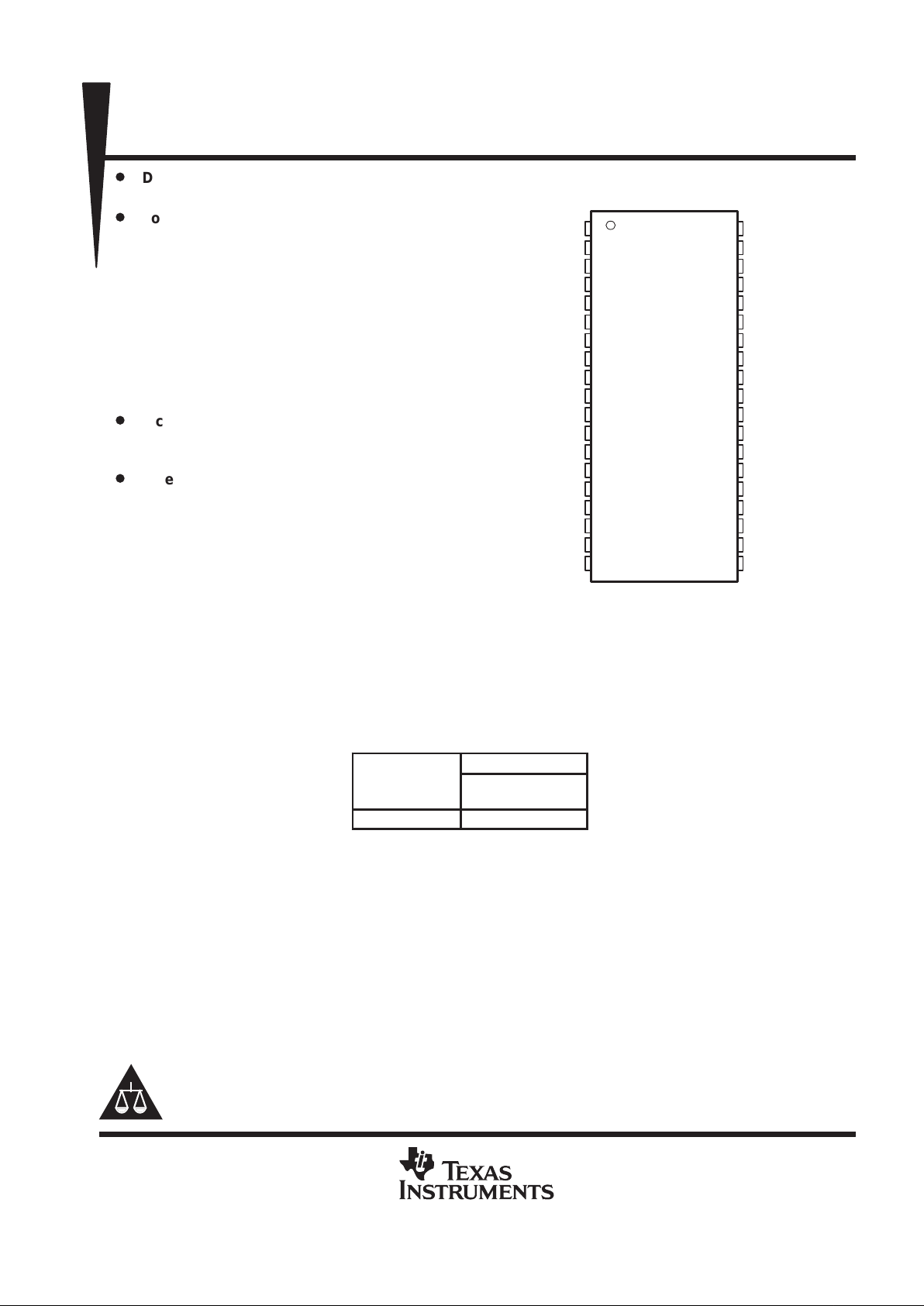
LOGIC V
DD1
SELECT1
VCO OUT1
F
IN
–A1
F
IN
–B1
PFD OUT1
LOGIC GND1
GND
NC
NC
NC
GND
LOGIC V
DD2
SELECT2
VCO OUT2
F
IN
–A2
F
IN
–B2
PFD OUT2
LOGIC GND2
VCO V
DD1
BIAS1
VCOIN1
VCO GND1
VCOINHIBIT1
PFD INHIBIT1
NC
GND
NC
NC
NC
GND
VCO V
DD2
BIAS2
VCOIN2
VCO GND2
VCOINHIBIT2
PFD INHIBIT2
NC
DB PACKAGE
(TOP VIEW)
NC – No internal connection
TLC2942
HIGH-PERFORMANCE DUAL PHASE-LOCKED LOOP BUILDING BLOCK
SLAS146B – NOVEMBER 1996 – REVISED JUNE 1997
2
POST OFFICE BOX 655303 • DALLAS, TEXAS 75265
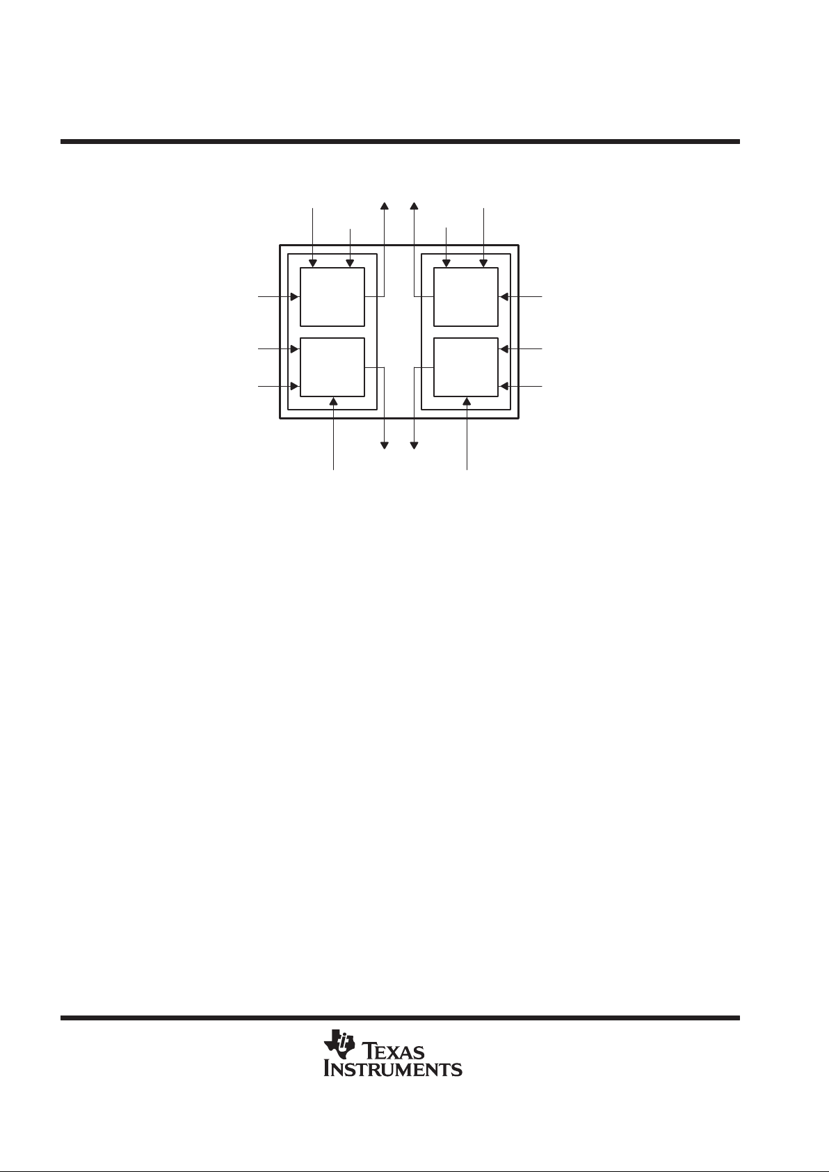
functional block diagram
SELECT1
SELECT2
VCO_1 VCO_2
PFD_1 PFD_2
VCO
INHIBIT1
VCO
INHIBIT2
VCO OUT1 VCO OUT2
PFD OUT1 PFD OUT2
PFD INHIBIT1 PFD INHIBIT2
VCOIN1
FIN–A1
FIN–B1
VCOIN2
FIN–A2
FIN–B2
34 1523 2214
24
16
17
1833 6 21
36
4
5
TLC2942
HIGH-PERFORMANCE DUAL PHASE-LOCKED LOOP BUILDING BLOCK
SLAS146B – NOVEMBER 1996 – REVISED JUNE 1997
3
POST OFFICE BOX 655303 • DALLAS, TEXAS 75265
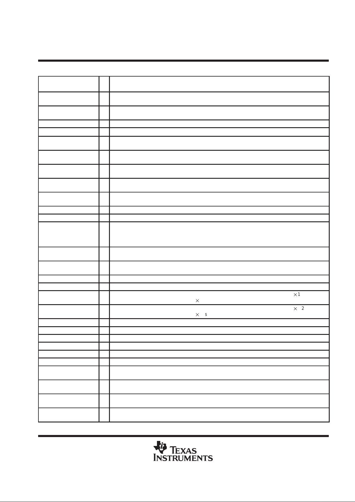
Terminal Functions
TERMINAL
I/
NAME NO.
O
DESCRIPTION
BIAS1 37 I VCO1 bias supply. An external resistor (R
BIAS
1) between VCO V
DD1
and BIAS1 supplies bias for adjusting
the oscillation frequency range.
BIAS2 25 I VCO2 bias supply. An external resistor (R
BIAS2
) between VCO V
DD2
and BIAS2 supplies bias for adjusting
the oscillation frequency range.
FIN–A1 4 I Input reference frequency 1. The frequency f(REF IN)1 is applied to FIN-A1.
FIN–A2 16 I Input reference frequency 2. The frequency f(REF IN)2 is applied to FIN-A2.
FIN–B1 5 I Input for VCO1 external counter output frequency f(FIN-B)1. FIN-B1 is nominally provided from the external
counter (see Figure 28).
FIN–B2 17 I Input for VCO2 external counter output frequency f(FIN-B)2. FIN-B2 is nominally provided from the external
counter (see Figure 28).
GND 8, 12,
27,31
Ground
LOGIC V
DD1
1 Logic1 supply voltage. LOGIC V
DD1
supplies voltage to internal logic 1. LOGIC V
DD1
should be separate
from the other supply lines to reduce cross-coupling between power supplies.
LOGIC V
DD2
13 Logic2 supply voltage. LOGIC V
DD2
supplies voltage to internal logic 2. LOGIC V
DD2
should be separate
from the other supply lines to reduce cross-coupling between power supplies.
LOGIC GND1 7 Ground for the internal logic 1
LOGIC GND2 19 Ground for the internal logic 2
NC 9, 10, 11,
20, 28,
29, 30,
32
No internal connection
PFD INHIBIT1 33 I PFD inhibit 1 control. When PFD INHIBIT1 is high, PFD OUT1 is in the high-impedance state (see
Table 4).
PFD INHIBIT2 21 I PFD inhibit 2 control. When PFD INHIBIT2 is high, PFD OUT2 is in the high-impedance state (see
Table 5).
PFD OUT1 6 O PFD1 output. When the PFD INHIBIT1 is high, PFD OUT1 is in the high-impedance state.
PFD OUT2 18 O PFD2 output. When the PFD INHIBIT2 is high, PFD OUT2 is in the high-impedance state.
SELECT1 2 I VCO1 output frequency select. When SELECT1 is high, the VCO1 output frequency is 1/2 and when
SELECT1 is low, the output frequency is 1 (see Table 1).
SELECT2 14 I VCO2 output frequency select. When SELECT2 is high, the VCO2 output frequency is 1/2 and when
SELECT2 is low, the output frequency is 1 (see Table 1).
VCO GND1 35 Ground for VCO1
VCO GND2 23 Ground for VCO2
VCOINHIBIT1 34 I VCO1 inhibit control. When VCOINHIBIT1 is high, VCO OUT1 is low (see Table 2).
VCOINHIBIT2 22 O VCO2 inhibit control. When VCOINHIBIT2 is high, VCO OUT2 is low (see Table 3).
VCO OUT1 3 O VCO1 output. When VCOINHIBIT1 is high, VCO OUT1 is low.
VCO OUT2 15 VCO2 output. When VCOINHIBIT2 is high, VCO OUT2 is low.
VCO V
DD1
38 VCO1 supply voltage. VCO V
DD1
supplies voltage for VCO1. VCO V
DD1
should be separated from LOGIC
V
DD1
and LOGIC V
DD2
and VCO VDD2 to reduce cross-coupling between power supplies.
VCO V
DD2
26 VCO2 supply voltage. VCO V
DD2
supplies voltage for VCO2. VCO V
DD2
should be separated from LOGIC
V
DD1
and LOGIC V
DD2
and VCO VDD1 to reduce cross-coupling between power supplies.
VCOIN1 36 I VCO1 control voltage input. Nominally the external loop filter output1 connects to VCOIN1 to control VCO1
oscillation frequency .
VCOIN2 24 I VCO2 control voltage input. Nominally the external loop filter output2 connects to VCOIN2 to control VCO2
oscillation frequency .
TLC2942
HIGH-PERFORMANCE DUAL PHASE-LOCKED LOOP BUILDING BLOCK
SLAS146B – NOVEMBER 1996 – REVISED JUNE 1997
4
POST OFFICE BOX 655303 • DALLAS, TEXAS 75265
detailed description
multichip module
The TLC2942 is a multichip module (MCM) product that uses two TLC2932 chips. A newly developed lead frame
for TLC2942IBD is specially shaped and cut in the package to electrically isolate one chip from another. The
two chips are completely independent from each other to perform the best stable oscillation and locking. If
asynchronous locking operation is required for these two PLL blocks, each TLC2942 VCO and PFD can achieve
the same stability as the single chip TLC2932IPW.
Three NC terminals are on both sides of the package between chip1 and chip2 due to the lead frame shape.
To avoid performance degradation, special attention is needed for each PLL block PCB layout especially for
supply voltage lines and GND patterns.
voltage-controlled oscillator (VCO)
VCO1 and VCO2 have the same typical characteristics. Each VCO oscillation frequency is determined by an
external resistor (R
BIAS
) connected between each VCO VDD and BIAS terminals. The oscillation frequency and
range depends on this register value. The bias resistor value for the minimum temperature coefficient is
nominally 3.3 kΩ with V
DD
= 3 V and nominally 2.2 kΩ with VDD = 5 V. For the lock frequency range refer to
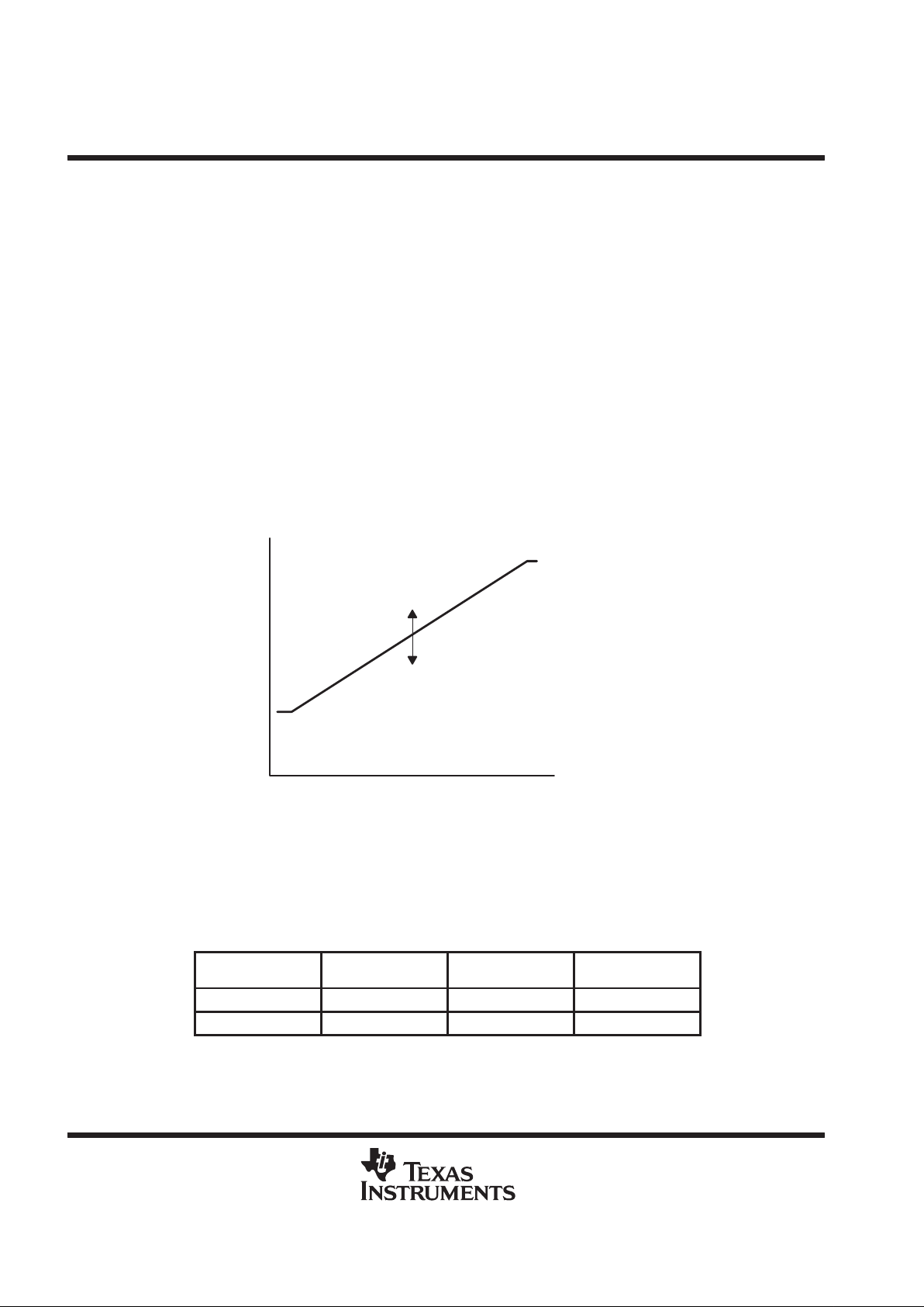
the recommended operating conditions. Figure 1 shows the typical frequency variation and VCO control
voltage.
VCO Oscillation Frequency Range
Bias Resistor (R
BIAS
)
1/2 V
DD
VCO Control Voltage (VCOIN)
VCO Oscillation Frequency
(f )
osc
Figure 1. VCO1 and VCO2 Oscillation Frequency
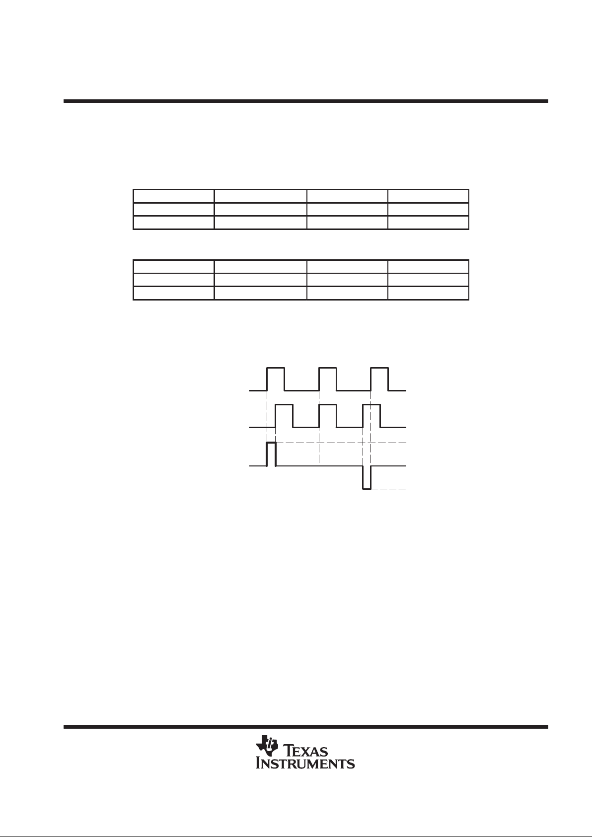
VCO output frequency 1/2 divider
SELECT1 and SELECT2 select between f
osc
and 1/2 f
osc
for the VCO output frequencies as shown in T able 1.
Table 1. SELECT1 and SELECT2 Function Table
SELECT1
VCO1 OUTPUT
FREQUENCY
SELECT2
VCO2 OUTPUT
FREQUENCY
Low
f
osc1
Low f
osc2
High
1/2 f
osc1
High 1/2 f
osc2
TLC2942
HIGH-PERFORMANCE DUAL PHASE-LOCKED LOOP BUILDING BLOCK
SLAS146B – NOVEMBER 1996 – REVISED JUNE 1997
5
POST OFFICE BOX 655303 • DALLAS, TEXAS 75265
VCO inhibit function
Each VCO has an externally controlled inhibit function that inhibits the VCO output. The VCO oscillation is
stopped during a high level on VCOINHIBIT , so the high level can also be used as the power-down mode. The
VCO output maintains a low level during the power-down mode (see Table 2 and Table 3).
Table 2. VCO1 Inhibit Function
VCOINHIBIT1 VCO1 OSCILLAT OR VCO OUT1 VCO1 I
DD
Low Active Active Normal
High Stop Low Power Down
Table 3. VCO2 Inhibit Function
VCOINHIBIT2 VCO2 OSCILLAT OR VCO OUT2 VCO2 I
DD
Low Active Active Normal
High Stop Low Power Down
PFD operation
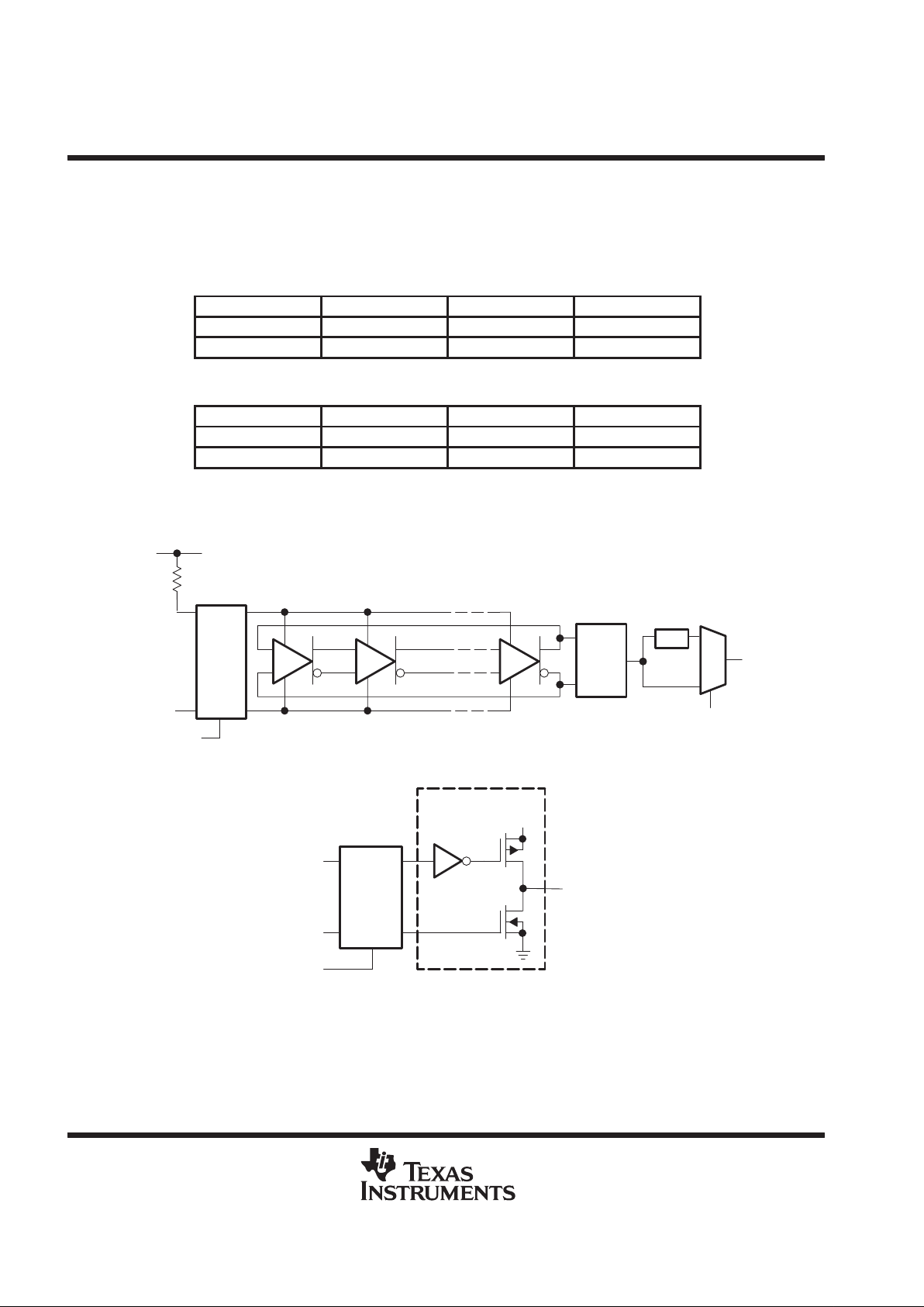
The PFD is a high-speed, edge-triggered detector with an internal charge pump. The PFD detects the phase
difference between two frequency inputs supplied to F
IN
–A and FIN–B as shown in Figure 2. Nominally the
reference is supplied to F
IN
–A, and the frequency from the external counter output is fed to FIN–B.
FIN–A1,
FIN–A2
FIN–B1,
FIN–B2
PFD OUT1,
PFD OUT2
V
OH
Hi-Z
V
OL
Figure 2. PFD Function Timing Chart
TLC2942
HIGH-PERFORMANCE DUAL PHASE-LOCKED LOOP BUILDING BLOCK
SLAS146B – NOVEMBER 1996 – REVISED JUNE 1997
6
POST OFFICE BOX 655303 • DALLAS, TEXAS 75265
PFD output control
A high level on PFD INHIBIT places the PFD OUT in the high-impedance state and the PFD stops phase
detection as shown in Table 4 and Table 5. A high level on PFD INHIBIT also can be used as the power-down
mode for the PFD.
Table 4. PFD1 Inhibit Function
PFD INHIBIT1 DETECTION PFD OUT1 PFD1 I
DD
Low Active Active Normal
High Stop Hi-Z Power Down
Table 5. PFD2 Inhibit Function Table
PFD INHIBIT2 DETECTION PFD OUT2 PFD2 I
DD
Low Active Active Normal
High Stop Hi-Z Power Down
schematics
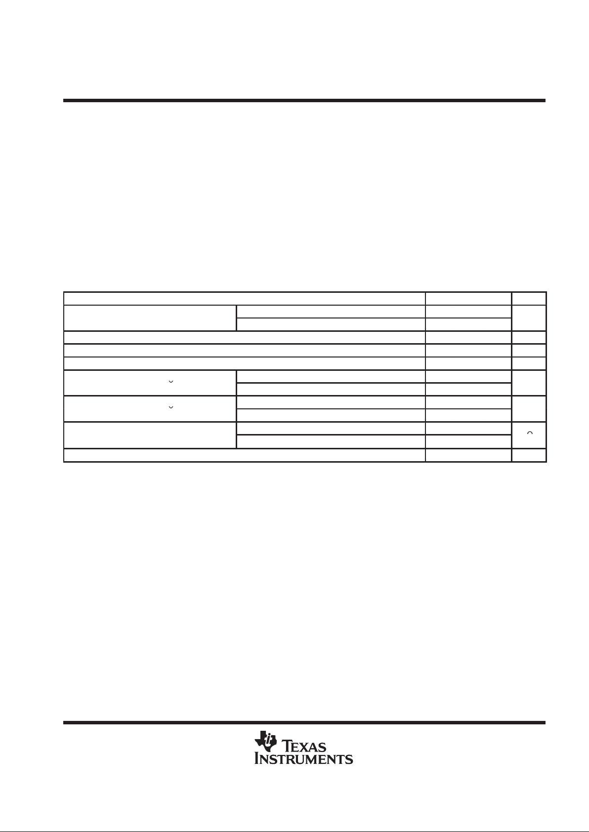
VCO block schematic (VCO1, VCO2)
Bias
Circuit
VCO
Output
1/2
R
BIAS
VCOIN1,
VCOIN2
(VCO control)
VCOINHIBIT
VCO OUT1,
VCO OUT2
SELECT1,2
M
U
X
Ring Oscillator
PFD block schematic (PFD1, PFD2)
Detector
Charge Pump
PFD OUT
FIN–A
FIN–B
PFD INHIBIT
V
DD
TLC2942
HIGH-PERFORMANCE DUAL PHASE-LOCKED LOOP BUILDING BLOCK
SLAS146B – NOVEMBER 1996 – REVISED JUNE 1997
7
POST OFFICE BOX 655303 • DALLAS, TEXAS 75265
absolute maximum ratings over operating free-air temperature range (unless otherwise noted)
†
Supply voltage (each supply), V
DD
(see Note 1) 7 V. . . . . . . . . . . . . . . . . . . . . . . . . . . . . . . . . . . . . . . . . . . . . . . .
Input voltage range (each input), V
I
(see Note 1) –0.5 V to V
DD
+ 0.5 V. . . . . . . . . . . . . . . . . . . . . . . . . . . . . . .
Input current (each input), I
I
±20 mA. . . . . . . . . . . . . . . . . . . . . . . . . . . . . . . . . . . . . . . . . . . . . . . . . . . . . . . . . . . . . .
Output current (each output), I
O
±20 mA. . . . . . . . . . . . . . . . . . . . . . . . . . . . . . . . . . . . . . . . . . . . . . . . . . . . . . . . . .
Continuous total power dissipation, at (or below) T
A
= 25°C (see Note 2) 1160 mW. . . . . . . . . . . . . . . . . . . . . .
Operating free-air temperature range, T
A
–20°C to 75°C. . . . . . . . . . . . . . . . . . . . . . . . . . . . . . . . . . . . . . . . . . . .
Storage temperature range, T
stg
–65°C to 150°C. . . . . . . . . . . . . . . . . . . . . . . . . . . . . . . . . . . . . . . . . . . . . . . . . . .
Lead temperature 1,6 mm (1/16 inch) from case for 10 seconds 260°C. . . . . . . . . . . . . . . . . . . . . . . . . . . . . . .
†
Stresses beyond those listed under “absolute maximum ratings” may cause permanent damage to the device. These are stress ratings only, and
functional operation of the device at these or any other conditions for extended periods may affect device reliability.
NOTES: 1. All voltage values are with respect to network GND.
2. For operation above 25°C free-air temperature, derate linearly at the rate of 9.3 mW/°C.
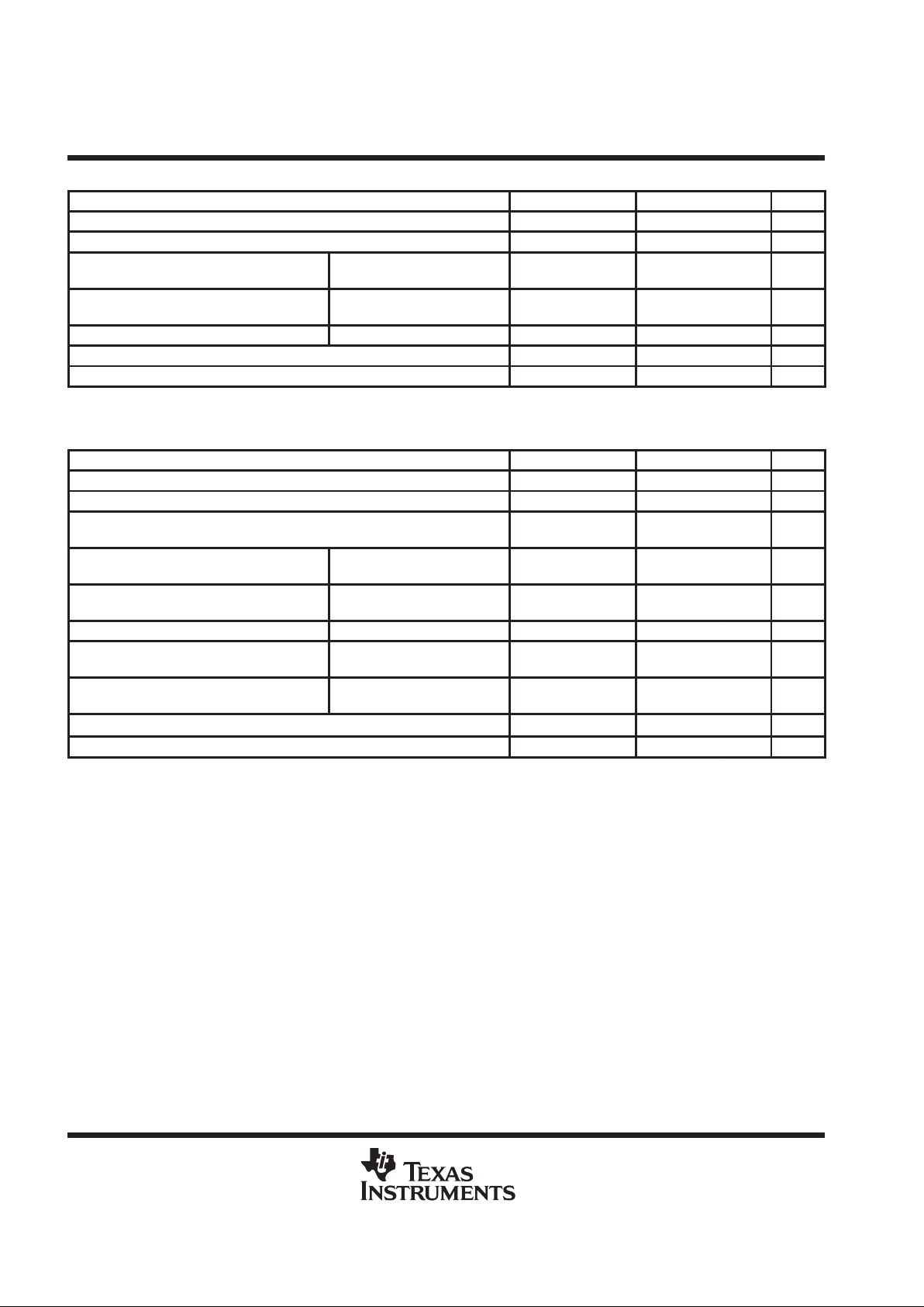
recommended operating conditions
MIN NOM MAX UNIT
pp
pp
VDD = 3 V 2.85 3 3.15
Suppl
y v
oltage, V
DD
(each suppl
y,
see Note 3)
VDD = 5 V 4.75 5 5.25
V
Input voltage, VI, (all inputs except VCOIN1, VCOIN2) 0 V
DD
V
Output current, IO (each output) 0 ±2 mA
VCO control voltage at each VCOIN1, VCOIN2 0.9 V
DD
V
p
VDD = 3 V 14 21
Lock frequenc
y,
(each VCO) (×1 output)
VDD = 5 V 22 50
MH
z
p
VDD = 3 V 7 10.5
Lock frequenc
y,
(each VCO) (×1/2 output)
VDD = 5 V 11 25
MH
z
VDD = 3 V 2.2 3.3 4.3
Bias resistor, (each BIAS), R
BIAS1,
R
BIAS2
VDD = 5 V 1.5 2.2 3.3
kΩ
Operating temperature, T
A
–20 75 °C
NOTE 3: It is recommended that LOGIC V
DD1
and VCO V
DD1
or LOGIC V
DD2
and VCO V
DD2
should be at the same voltage and separated from
each other.
TLC2942
HIGH-PERFORMANCE DUAL PHASE-LOCKED LOOP BUILDING BLOCK
SLAS146B – NOVEMBER 1996 – REVISED JUNE 1997
8
POST OFFICE BOX 655303 • DALLAS, TEXAS 75265
VCO1, VCO2 electrical characteristics, V
DD
= 3 V, T
A
= 25°C (unless otherwise noted)
PARAMETER TEST CONDITIONS MIN TYP MAX UNIT
V
OH
High-level output voltage IOH = –2 mA 2.4 V
V
OL
Low-level output voltage IOL = 2 mA 0.3 V
V
IT
Input threshold voltage
SELECT1, SELECT2,
VCOINHIBIT2, VCOINHIBIT1
0.9 1.5 2.1 V
I
I
Input current
SELECT1, SELECT2,
VCOINHIBIT2, VCOINHIBIT1
VI = VDD or GND ±1 µA
Z
i(VCOIN)
Input impedance VCOIN2, VCOIN1 VCOIN = 1/2 V
DD
10 MΩ
I
DD(INH)
VCO supply current (inhibit) (each chip) See Note 4 0.01 1 µA
I
DD(VCO)
VCO supply current (each chip) See Note 5 5 15 mA
NOTES: 4. The current into VCO VDD and LOGIC VDD when VCOINHIBIT = VDD, and the PFD is inhibited.
5. The current into VCO VDD and LOGIC VDD when VCOIN = 1/2 VDD, R
BIAS
= 3.3 kΩ, VCOINHIBIT = GND, and the PFD is inhibited.
PFD1, PFD2 electrical characteristic, V
DD
= 3 V, T
A
= 25°C (unless otherwise noted)
PARAMETER TEST CONDITIONS MIN TYP MAX UNIT
V
OH
High-level output voltage IOH = –2 mA 2.7 V
V
OL
Low-level output voltage IOL = 2 mA 0.2 V
I
OZ
High-impedance output current
PFD INHIBIT = high,
VO = VDD or GND
±1 µA
V
IH
High-level input voltage
FIN–A1, FIN–B1,
FIN–A2, FIN–B2
2.7 V
V
IL
Low-level input voltage
FIN–A1, FIN–B1,
FIN–A2, FIN–B2
0.5 V
V
IT
Input threshold voltage PFD INHIBIT2, PFD INHIBIT1 0.9 1.5 2.1 V
C
i
Input capacitance
FIN–A1, FIN–B1,
FIN–A2, FIN–B2
5 pF
Z
i
Input impedance
FIN–A1, FIN–B1,
FIN–A2, FIN–B2
10 MΩ
I
DD(Z)
High-impedance state PFD supply current See Note 6 0.1 1 µA
I
DD(PFD)
PFD supply current See Note 7 0.1 1.5 mA
NOTES: 6. The current into LOGIC VDD, when FIN–A and FIN–B = GND, PFD INHIBIT= VDD, no load, and VCO OUT is inhibited.
7. The current into LOGIC VDD when FIN–A and FIN–B = 1 MHz with V
I(PP)
= 3 V rectangular wave, PFD INHIBIT = GND, no load,
and VCO OUT is inhibited.
TLC2942
HIGH-PERFORMANCE DUAL PHASE-LOCKED LOOP BUILDING BLOCK
SLAS146B – NOVEMBER 1996 – REVISED JUNE 1997
9
POST OFFICE BOX 655303 • DALLAS, TEXAS 75265
VCO1, VCO2 operating characteristics, V
DD
= 3 V, T
A
= 25°C (unless otherwise noted)
PARAMETER TEST CONDITIONS MIN TYP MAX UNIT
f
osc
Operating oscillation frequency
R
BIAS1, RBIAS2
= 3.3 kΩ,
VCOIN1, VCOIN2 = 1/2 V
DD
15 19 23 MHz
t
s(fosc)
Time to stable oscillation See Note 8 10 µs
CL = 15 pF, See Figure 3 7 14
trRise time
CL = 50 pF, See Figure 3 14
ns
CL = 15 pF, See Figure 3 6 12
tfFall time
CL = 50 pF, See Figure 3 10
ns
Duty cycle at VCO OUT
R
BIAS1
, R
BIAS2
= 3.3 kΩ,
VCOIN1, VCOIN2 = 1/2 V
DD
45% 50% 55%
α
(fosc)
Temperature coefficient of oscillation frequency
R
BIAS1, RBIAS2
= 3.3 kΩ,
VCOIN1, VCOIN2 = 1/2 VDD,
TA = –20°C to 75°C
0.04 %/°C
k
SVS(fosc)
Supply voltage coefficient of oscillation frequency
R
BIAS1,
R
BIAS2
= 3.3 kΩ,
VCOIN1, VCOIN2 = 1.5 V,
VDD = 2.85 V to 3.15 V
0.02 %/mV
Jitter absolute (see Note 9) R
BIAS1
= 3.3 kΩ 100 ps
NOTES: 8. The time period to stabilize the VCO oscillation frequency after VCOINHIBIT is changed to a low level.
9. The LPF circuit is shown in Figure 28 with calculated values listed in Table 9. Jitter performance is highly dependent on circuit layout
and external device characteristics. The jitter specification was made with a carefully designed PCB with no device socket.
PFD1, PFD2 operating characteristics, V
DD
= 3 V, T
A
= 25°C (unless otherwise noted)
PARAMETER TEST CONDITIONS MIN TYP MAX UNIT
f
max
Maximum operating frequency 20 MHz
t
PLZ
PFD output disable time from low level 21 50
t
PHZ
PFD output disable time from high level
23 50
ns
t
PZL
PFD output enable time to low level
See Figures 4 and 5 and Table 4
11 30
t
PZH
PFD output enable time to high level 10 30
ns
t
r
Rise time
p
2.3 10 ns
t
f
Fall time
C
L
= 15 pF,
See Figure 4
2.1 10 ns
 Loading...