Texas Instruments TL7770-5QDWR, TL7770-5QDW, TL7770-5MFKB, TL7770-5MJB, TL7770-5QN Datasheet

TL7770-5, TL7770-12
DUAL POWER-SUPPLY SUPERVISORS
SLVS019F – OCTOBER 1987 – REVISED JULY 1999
D
Power-On Reset Generator
D
Automatic Reset Generation After Voltage
Drop
D
RESET Defined When VCC Exceeds 1 V
D
Wide Supply-Voltage Range . . . 3.5 V
to 18 V
D
Precision Overvoltage and Undervoltage
Sensing
D
250-mA Peak Output Current for Driving
SCR Gates
D
2-mA Active-Low SCR Gate Drive for
1SCR DRIVE
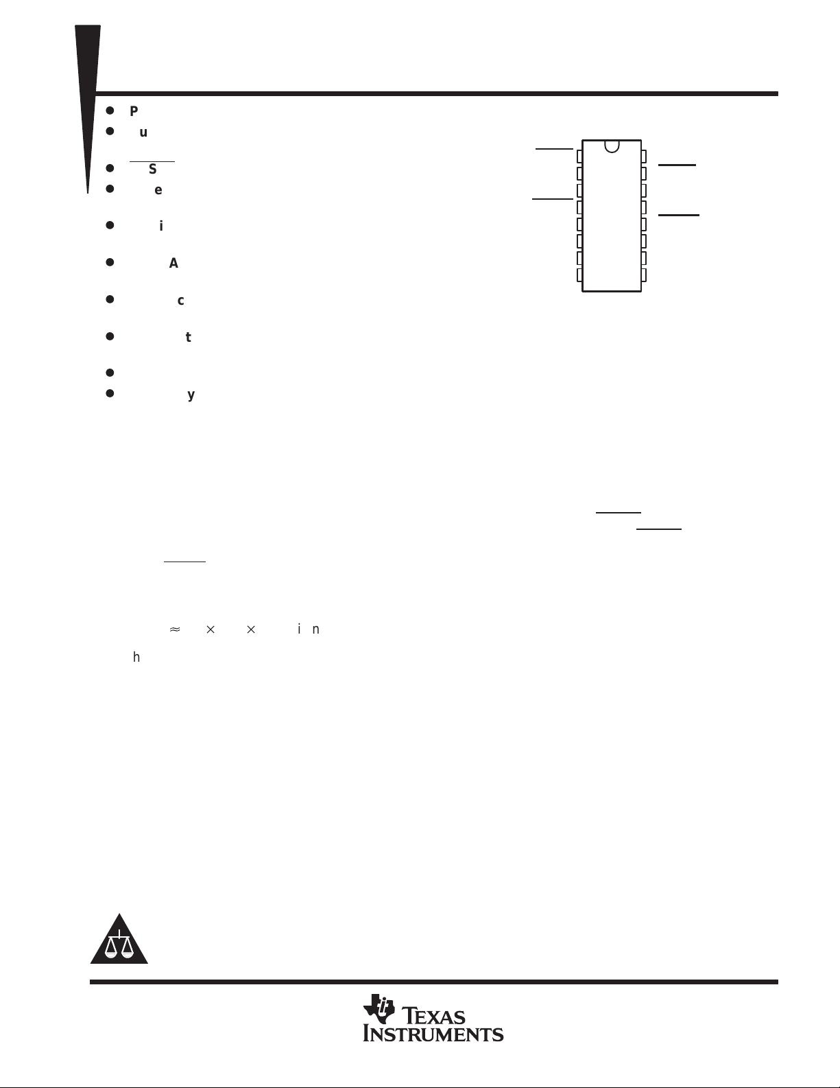
DW OR N PACKAGE
(TOP VIEW)
1RESIN
1CT
1RESET
1RESET
1VSU
1VSO
GND
1
2
3
4
5
6
7
8
CC
2RESIN
15
2CT
14
2RESET
13
2RESET
12
2VSU
11
2VSO
10
2SCR DRIVE
9
V
16
False-Trigger Protection
D
T emperature-Compensated Voltage
Reference
D
True and Complementary Reset Outputs
D
Externally Adjustable Output Pulse
Duration
description
The TL7770 is an integrated-circuit system supervisor designed for use as a reset controller in microcomputer
and microprocessor power-supply systems. This device contains two independent supply-voltage supervisors
that monitor the supplies for overvoltage and undervoltage conditions at the VSO and VSU terminals,
respectively . When V
(low). As VCC approaches 3.5 V , the time-delay function activates, latching RESET and RESET active (high and
low, respectively) for a time delay (td) after system voltages have achieved normal levels. Above VCC = 3.5 V,
taking RESIN low activates the time-delay function during normal system-voltage levels. To ensure that the
microcomputer system has reset, the outputs remain active until the voltage at VSU exceeds the threshold
value, V
, for a time delay, which is determined by an external timing capacitor such that:
IT+
attains the minimum voltage of 1 V during power up, the RESET output becomes active
CC
td[20
103
capacitance
where td is in seconds and capacitance is in farads.
The overvoltage-detection circuit is programmable for a wide range of designs. During an overvoltage condition,
an internal silicon-controlled rectifier (SCR) is triggered, providing 250-mA peak instantaneous current and
25-mA continuous current to the SCR gate drive terminal, which can drive an external high-current SCR gate
or an overvoltage-warning circuit.
The TL7770C series is characterized for operation from 0°C to 70°C. The TL7770I series is characterized for
operation from –40°C to 85°C.
Please be aware that an important notice concerning availability, standard warranty, and use in critical applications of
Texas Instruments semiconductor products and disclaimers thereto appears at the end of this data sheet.
PRODUCTION DATA information is current as of publication date.
Products conform to specifications per the terms of Texas Instruments
standard warranty. Production processing does not necessarily include
testing of all parameters.
Copyright 1999, Texas Instruments Incorporated
POST OFFICE BOX 655303 • DALLAS, TEXAS 75265
1

TL7770-5, TL7770-12
CHIP FORM
DUAL POWER-SUPPLY SUPERVISORS
SLVS019F – OCTOBER 1987 – REVISED JULY 1999
T
A
0°C to 70°C
–40°C to 85°C TL7770-5IDW TL7770-5IN —
DW package is available taped and reeled. Add the suffix R to the device type
(e.g., TL7770-5CDWR). Chip forms are tested at 25°C.
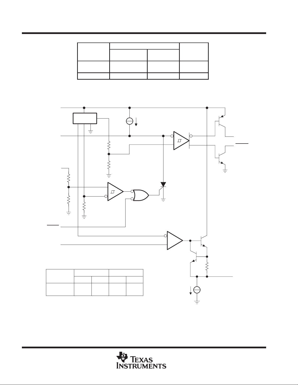
functional block diagram (each channel)
V
CC
V
ref
SMALL OUTLINE
TL7770-5CDW
TL7770-12CDW
AVAILABLE OPTIONS
PACKAGED DEVICES
PLASTIC DIP
(DW)
TL7770-5CN
TL7770-12CN
65 µA (TYP)
(N)
(Y)
TL7770-5Y
TL7770-12Y
CT
VSU
R1
R2
RESIN
VSO
DEVICE
TL7770-5
TL7770-12
†
The values listed are nominal.
1 VSU 2 VSU
†
R1
24 kΩ
70 kΩ
R2
10 kΩ
10 kΩ
†
R1 R2
Short
Short
Open
Open
RESET
RESET
SCR DRIVE
2 mA
(TYP)
2
POST OFFICE BOX 655303 • DALLAS, TEXAS 75265

ООООООО
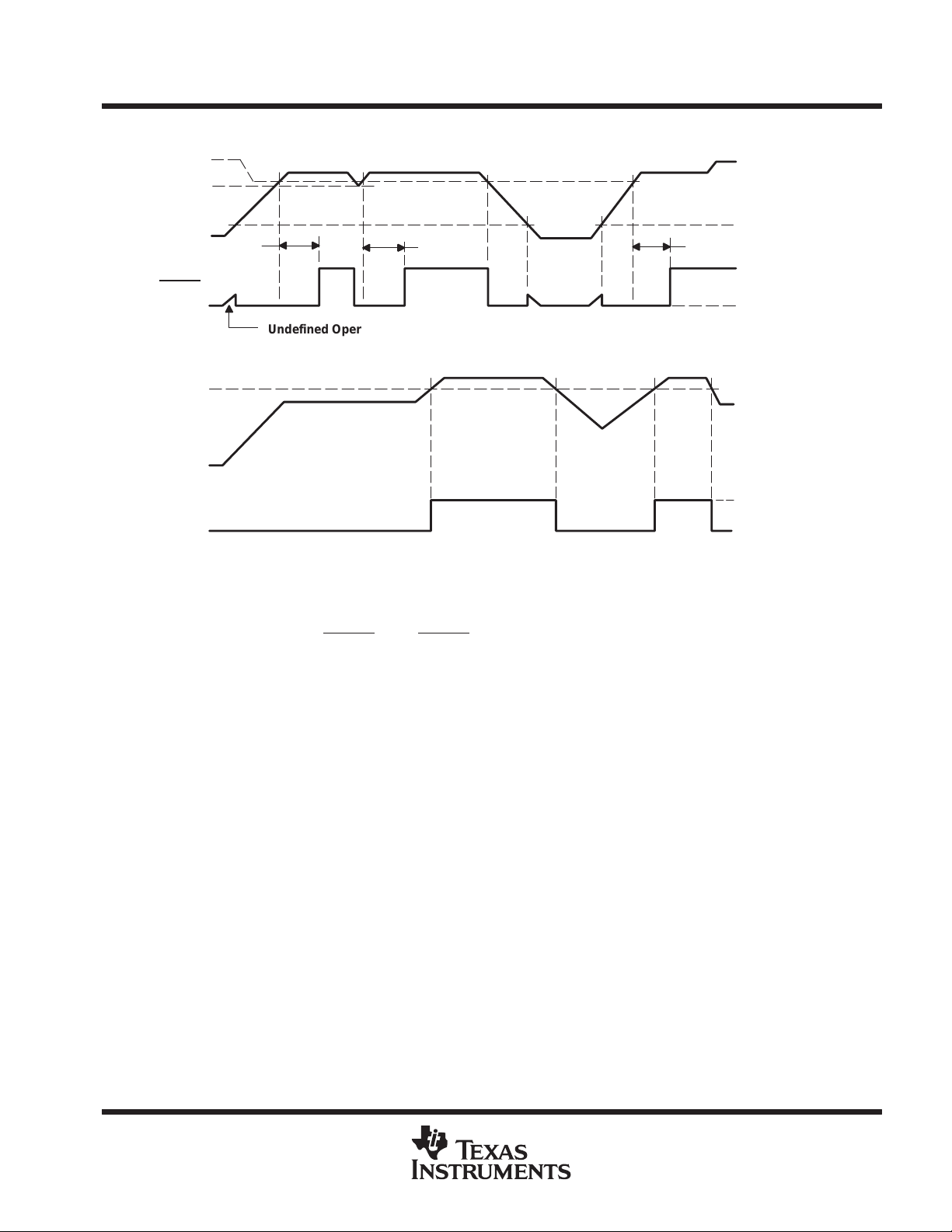
timing requirements
V
IT+
V
IT–
TL7770-5, TL7770-12
DUAL POWER-SUPPLY SUPERVISORS
SLVS019F – OCTOBER 1987 – REVISED JULY 1999
VSU
RESET
V
VSO
SCR DRIVE
t
d
Undefined Operation
for VCC Less Than 1 V
T
t
d
t
d
VCC = 1 V (TYP)
V
OH
V
OL
V
OH
V
OL
absolute maximum ratings over operating free-air temperature range (unless otherwise noted)
Supply voltage, VCC (see Note 1) 20 V. . . . . . . . . . . . . . . . . . . . . . . . . . . . . . . . . . . . . . . . . . . . . . . . . . . . . . . . . . . .
Input voltage range, VI: 1VSU, 2VSU, 1VSO, and 2VSO (see Note 1) –0.3 V to 18 V. . . . . . . . . . . . . . . . . . . .
Low-level output current (1RESET
High-level output current (1RESET and 2RESET), IOH –20 mA. . . . . . . . . . . . . . . . . . . . . . . . . . . . . . . . . . . . . . .
Package thermal impedance, θJA (see Notes 2 and 3): DW package 57°C/W. . . . . . . . . . . . . . . . . . . . . . . . . . .
Lead temperature 1,6 mm (1/16 in) from case for 10 seconds: DW or N package 260°C. . . . . . . . . . . . . . . . .
Storage temperature range, T
†
Stresses beyond those listed under “absolute maximum ratings” may cause permanent damage to the device. These are stress ratings only, and
functional operation of the device at these or any other conditions beyond those indicated under “recommended operating conditions” is not
implied. Exposure to absolute-maximum-rated conditions for extended periods may affect device reliability.
NOTES: 1. All voltage values are with respect to the network ground terminal.
2. Maximum power dissipation is a function of TJ(max),
ambient temperature is PD = (TJ(max) – TA)/
3. The package thermal impedance is calculated in accordance with JESD 51, except for through-hole packages, which use a trace
length of zero.
and 2RESET), IOL 20 mA. . . . . . . . . . . . . . . . . . . . . . . . . . . . . . . . . . . . . . . .
N package 88°C/W. . . . . . . . . . . . . . . . . . . . . . . . . . . .
–65°C to 150°C. . . . . . . . . . . . . . . . . . . . . . . . . . . . . . . . . . . . . . . . . . . . . . . . . . .
stg
θ
, and TA. The maximum allowable power dissipation at any allowable
θ
JA
JA
. Operating at the absolute maximum TJ of 150°C can impact reliability.
†
POST OFFICE BOX 655303 • DALLAS, TEXAS 75265
3
 Loading...