

www.DataSheet4U.com
www.ti.com
AUTOMOTIVE LOW-DROPOUT VOLTAGE REGULATORS
TL750M-Q1, TL751M-Q1 Series
SGLS312F – SEPTEMBER 2005 – REVISED JUNE 2007
FEATURES
• Low Quiescent Current
• Qualified for Automotive Applications • TTL- and CMOS-Compatible Enable on
• Customer-Specific Configuration Control Can
TL751M Series
Be Supported Along With Major-Change • Load-Dump Protection
Approval
• Low Dropout Voltage, Less Than 0.6 V at
750 mA
• Overvoltage Protection
• Internal Thermal Overload Protection
• Internal Overcurrent-Limiting Circuitry
DESCRIPTION
The TL750M and TL751M series are low-dropout positive voltage regulators specifically designed for automotive
applications. The TL750M and TL751M series incorporate onboard overvoltage and current-limiting protection
circuitry to protect the devices and the regulated system. Both series are fully protected against load-dump and
reverse-battery conditions. Load-dump protection is up to a maximum of 60 V at the input of the device. Low
quiescent current, even during full-load conditions, makes the TL750M and TL751M series ideal for use in
applications that are permanently connected to the vehicle battery.
The TL750M and TL751M series offers 5-V and 8-V options. The TL751M series has the addition of an enable
( ENABLE) input. The ENABLE input gives complete control over power up, allowing sequential power up or
shutdown. When ENABLE is high, the regulator output is placed in the high-impedance state. The ENABLE
input is TTL and CMOS compatible.
The TL750Mxx and TL751Mxx are characterized for operation over the virtual junction temperature range –40 ° C
to 125 ° C.
AVAILABLE OPTIONS
V
T
J
–40 ° C to 125 ° C
O
NOM (V)
5 TO-263-3/KTT, Reel of 500 TL750M05QKTTRQ1 TL750M05Q1
8 TO-263-3/KTT, Reel of 500 TL750M08QKTTRQ1 TL750M08Q1
5 TO-263-5/KTT, Reel of 500 TL751M05QKTTRQ1 TL751M05Q1
8 TO-263-5/KTT, Reel of 500 TL751M08QKTTRQ1 TL751M08Q1
PACKAGE ORDERABLE PART NUMBER TOP SIDE MARKING
Please be aware that an important notice concerning availability, standard warranty, and use in critical applications of Texas
Instruments semiconductor products and disclaimers thereto appears at the end of this data sheet.
PRODUCTION DATA information is current as of publication date.
Products conform to specifications per the terms of the Texas
Instruments standard warranty. Production processing does not
necessarily include testing of all parameters.
Copyright © 2005–2007, Texas Instruments Incorporated
www.ti.com
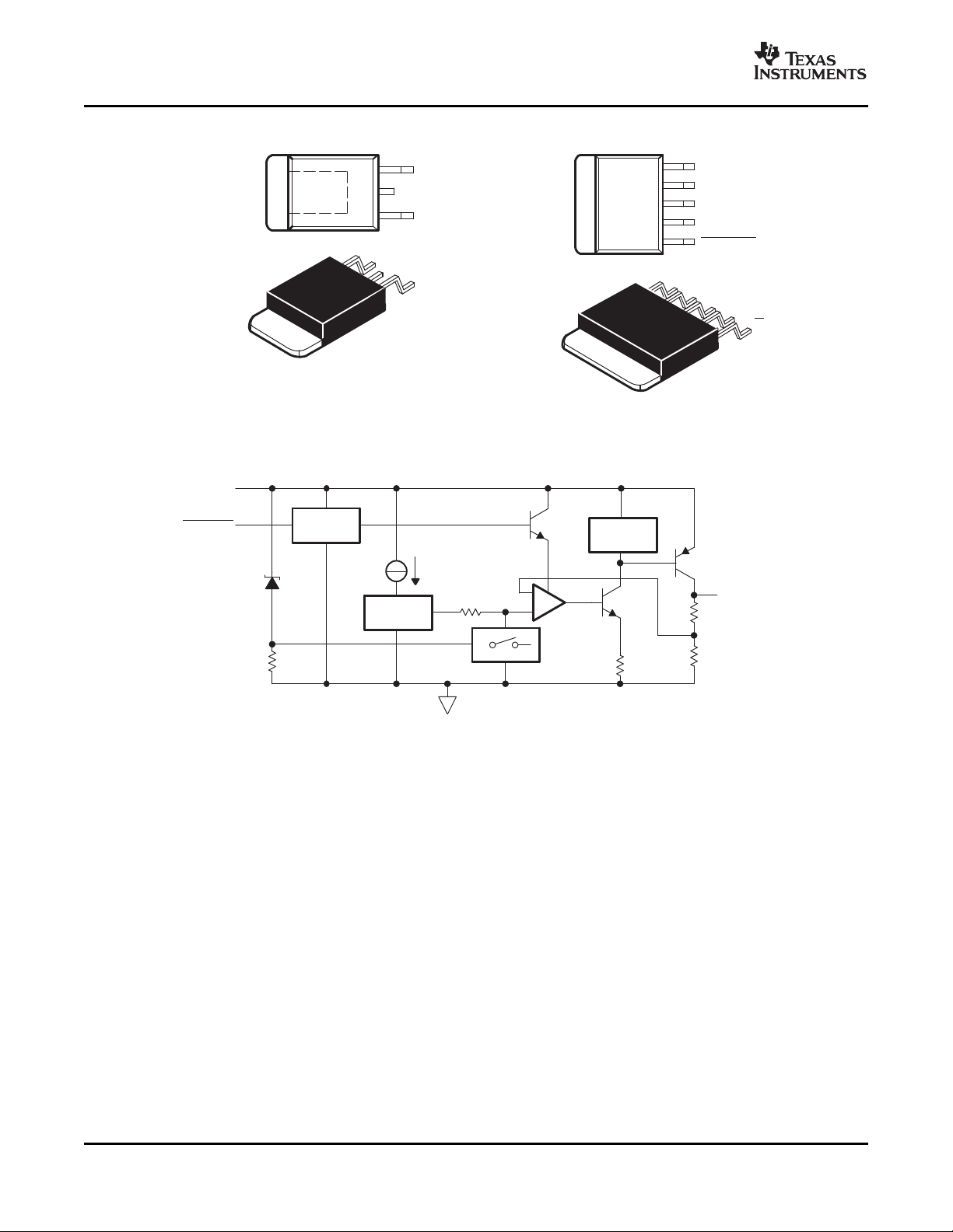
TL750M. . . KTT (3 Pin Shown)
(TOP VIEW)
OUTPUT
COMMON
INPUT
COMMON
O
C
I
TL751M. . . KTT (5 Pin Shown)
(TOP VIEW)
NC
OUTPUT
COMMON
INPUT
ENABLE
O
C
I
N
E
Enable
Bandgap
Current
Limiting
_
+
Overvoltage/
Thermal
Shutdown
ENABLE
OUTPUT
COMMON
INPUT
28 V
TL750M-Q1, TL751M-Q1 Series
SGLS312F – SEPTEMBER 2005 – REVISED JUNE 2007
A. The COMMON terminal is in electrical contact with the mounting base.
NC – No internal connection
TL751Mxx FUNCTIONAL BLOCK DIAGRAM
2
Submit Documentation Feedback
www.ti.com
TL750M-Q1, TL751M-Q1 Series
SGLS312F – SEPTEMBER 2005 – REVISED JUNE 2007
ABSOLUTE MAXIMUM RATINGS
over operating free-air temperature range (unless otherwise noted)
Continuous input voltage 26 V
Transient input voltage (see Figure 4 ) 60 V
Continuous reverse input voltage –15 V
Transient reverse input voltage t = 100 ms –50 V
θ
JA
T
J
T
stg
Package thermal impedance
Virtual junction temperature range –40 ° C to 150 ° C
Storage temperature range –65 ° C to 150 ° C
(2) (3)
(1) Stresses beyond those listed under absolute maximum ratings may cause permanent damage to the device. These are stress ratings
only, and functional operation of the device at these or any other conditions beyond those indicated under recommended operating
conditions is not implied. Exposure to absolute-maximum-rated conditions for extended periods may affect device reliability.
(2) Maximum power dissipation is a function of TJ(max), θJA, and TA. The maximum allowable power dissipation at any allowable ambient
temperature is PD= (TJ(max) – TA)/ θJA. Operating at the absolute maximum TJof 150 ° C can impact reliability. Due to variation in
individual device electrical characteristics and thermal resistance, the built-in thermal overload protection may be activated at power
levels slightly above or below the rated dissipation.
(3) The package thermal impedance is calculated in accordance with JESD 51.
RECOMMENDED OPERATING CONDITIONS
V
I
V
IH
V
IL
I
O
T
J
Input voltage V
High-level ENABLE input voltage TL751Mxx 2 15 V
Low-level ENABLE input voltage TL751Mxx 0 0.8 V
Output current TL75xMxx 750 mA
Operating virtual junction temperature TL75xMxx –40 125 ° C
(1)
VALUE / UNIT
KTT package (3 pin) 26.9 ° C/W
KTT package (5 pin) 26.5 ° C/W
MIN MAX UNIT
TL75xM05 6 26
TL75xM08 9 26
TL751Mxx ELECTRICAL CHARACTERISTICS
VI= 14 V, IO= 300 mA, TJ= 25 ° C
PARAMETER UNIT
Response time, ENABLE to output (start-up) 50 µs
TL751Mxx
TYP
Submit Documentation Feedback
3
www.ti.com
TL750M-Q1, TL751M-Q1 Series
SGLS312F – SEPTEMBER 2005 – REVISED JUNE 2007
TL750M05/TL751M05 ELECTRICAL CHARACTERISTICS
VI= 14 V, IO= 300 mA, ENABLE at 0 V for TL751M05, TJ= –40 ° C to 125 ° C (unless otherwise noted)
PARAMETER TEST CONDITIONS UNIT
Output voltage VI= 6 V to 26 V 4.85 5 5.15 V
Line regulation mV
Power-supply ripple rejection VI= 8 V to 18 V, f = 120 Hz 55 dB
Load regulation IO= 5 mA to 750 mA 20 50 mV
Dropout voltage
Current consumption
Iq= II– I
Shutdown current (TL751M05 only) ENABLE VIH≥ 2 V 200 µA
(1) Pulse-testing techniques maintain the junction temperature as close to the ambient temperature as possible. Thermal effects must be
taken into account separately. All characteristics are measured with a 0.1-µF capacitor across the input and a 10-µF tantalum capacitor
on the output, with equivalent series resistance within the guidelines shown in Figure 4 .
(2) Measured when the output voltage, VO, has dropped 100 mV from the nominal value obtained at VI= 14 V
(2)
O
VI= 9 V to 16 V, IO= 250 mA 10 25
VI= 6 V to 26 V, IO= 250 mA 12 50
IO= 500 mA, TJ= 25 ° C 0.5
IO= 750 mA, TJ= 25 ° C 0.65
IO= 750 mA 60 75
IO= 10 mA 5
(1)
TL750M05
TL751M05
MIN TYP MAX
V
mA
TL750M08/TL751M08 ELECTRICAL CHARACTERISTICS
VI= 14 V, IO= 300 mA, ENABLE at 0 V for TL751M08, TJ= –40 ° C to 125 ° C (unless otherwise noted)
PARAMETER TEST CONDITIONS UNIT
Output voltage VI= 6 V to 26 V 7.76 8 8.24 V
Line regulation mV
Power-supply ripple rejection VI= 11 V to 21 V, f = 120 Hz 55 dB
Load regulation IO= 5 mA to 750 mA 24 80 mV
Dropout voltage
Current consumption
Iq= II– I
Shutdown current (TL751M08 only) ENABLE VIH≥ 2 V 200 µA
(1) Pulse-testing techniques maintain the junction temperature as close to the ambient temperature as possible. Thermal effects must be
taken into account separately. All characteristics are measured with a 0.1-µF capacitor across the input and a 10-µF tantalum capacitor
on the output, with equivalent series resistance within the guidelines shown in Figure 4 .
(2) Measured when the output voltage, VO, has dropped 100 mV from the nominal value obtained at VI= 14 V
(2)
O
VI= 10 V to 17 V, IO= 250 mA 12 40
VI= 9 V to 26 V, IO= 250 mA 15 68
IO= 500 mA, TJ= 25 ° C 0.5
IO= 750 mA, TJ= 25 ° C 0.65
IO= 750 mA, TJ= 25 ° C 60 75
IO= 10 mA 5
(1)
TL750M08
TL751M08
MIN TYP MAX
V
mA
4
Submit Documentation Feedback

www.ti.com
Applied Load
Current
Load
Voltage
∆V
L
∆I
L
∆VL = ∆IL × ESR
TL750M-Q1, TL751M-Q1 Series
SGLS312F – SEPTEMBER 2005 – REVISED JUNE 2007
PARAMETER MEASUREMENT INFORMATION
The TL750Mxx and TL751Mxx are low-dropout regulators. The output capacitor value and the parasitic
equivalent series resistance (ESR) affect the bandwidth and stability of the control loop for these devices. For
this reason, the capacitor and ESR must be carefully selected for a given operating temperature and load range.
Figure 2 and Figure 3 can be used to establish the appropriate capacitance value and ESR for the best regulator
transient response.
Figure 2 shows the recommended range of ESR for a given load with a 10-µF capacitor on the output. Figure 2
also shows a maximum ESR limit of 2 Ω and a load-dependent minimum ESR limit.
For applications with varying loads, the lightest load condition should be chosen because it is the worst case.
Figure 3 shows the relationship of the reciprocal of ESR to the square root of the capacitance, with a minimum
capacitance limit of 10 µF and a maximum ESR limit of 2 Ω . This figure establishes the amount that the
minimum ESR limit shown in Figure 2 can be adjusted for different capacitor values. For example, where the
minimum load needed is 200 mA, Figure 2 suggests an ESR range of 0.8 Ω to 2 Ω for 10 µF. Figure 3 shows
that changing the capacitor from 10 µF to 400 µF can change the ESR minimum by greater than 3/0.5 (or 6).
Therefore, the new minimum ESR value is 0.8/6 (or 0.13 Ω ). This allows an ESR range of 0.13 Ω to 2 Ω ,
achieving an expanded ESR range by using a larger capacitor at the output. For better stability in low-current
applications, a small resistance placed in series with the capacitor (see Table 1 ) is recommended, so that ESRs
better approximate those shown in Figure 2 and Figure 3 .
Table 1. Compensation for Increased Stability at Low Currents
MANUFACTURER CAPACITANCE ESR TYP PART NUMBER ADDITIONAL RESISTANCE
AVX 15 µF 0.9 Ω TAJB156M010S 1 Ω
KEMET 33 µF 0.6 Ω T491D336M010AS 0.5 Ω
Figure 1.
Submit Documentation Feedback
5

www.ti.com
2.5
0.4
0.3
0.2
0.1
0
0.10 0.2 0.3 0.4 0.5
I
L
- Load Current Rang e - A
This Region Not
Recommended for
Operation
CL= 10 µF
CI= 0.1 µF
f = 120 Hz
Equivalent Series Resistance (ESR) -
&
0.5
Potential Instability Region
Min ESR
Boundary
Max ESR Boundary
Region of Best Stability
0 1 2 3 4 54.53.52.51.50.5
0
0.01
0.015
0.02
0.025
0.03
0.035
0.04
200 µF
1000 µF
1/ESR
0.005
400 µF
Not Recommended
Recommended Min ESR
Potential Instability
Region of
Best Stability
100 µF
22 µF
10 µF
C
L
Stability −
TL750M-Q1, TL751M-Q1 Series
SGLS312F – SEPTEMBER 2005 – REVISED JUNE 2007
OUTPUT CAPACITOR EQUIVALENT
SERIES RESISTANCE (ESR) STABILITY
LOAD CURRENT RANGE EQUIVALENT SERIES RESISTANCE (ESR)
vs vs
6
Figure 2. Figure 3.
Submit Documentation Feedback

www.ti.com
30
20
0 100 200
40
60
300 400 500 600
I
V − Transient Input Voltage − V
0
10
50
TJ = 25°C
VI = 14 V + 46e
(−t/0.230)
for t ≥ 5 ms
t − Time − ms
t
r
= 1 ms
8
4
2
0
0 2 4 6 8 10
− Output Voltage − V
12
14
12 14
10
6
V
O
VI − Input Voltage − V
IO = 10 mA
TJ = 25°C
TL75xM08
TL75xM05
TL750M-Q1, TL751M-Q1 Series
SGLS312F – SEPTEMBER 2005 – REVISED JUNE 2007
TYPICAL CHARACTERISTICS
Table of Graphs
FIGURE
Transient input voltage vs Time 4
Output voltage vs Input voltage 5
Input current vs Input voltage
Dropout voltage vs Output current 8
Quiescent current vs Output current 9
Load transient response 10
Line transient response 11
IO= 10 mA 6
IO= 100 mA 7
TRANSIENT INPUT VOLTAGE OUTPUT VOLTAGE
vs vs
TIME INPUT VOLTAGE
Figure 4. Figure 5.
Submit Documentation Feedback
7

www.ti.com
80
40
20
0
0 2 4 6 8 10
120
140
12 14
100
60
180
200
160
− Input Current − mAI
I
VI − Input Voltage − V
IO = 10 mA
TJ = 25°C
TL75_M05
TL75_M08
200
100
50
0
0 2 4 6 8 10
300
350
12 14
250
150
VI − Input Voltage − V
IO = 100 mA
TJ = 25°C
− Input Current − mAI
I
TL75_M05
TL75_M08
200
150
125
100
0 50 100 150 200 250
250
300
225
175
75
50
IO − Output Current − mA
TJ = 25°C
Dropout Voltage − mV
12
8
6
4
0 20 40 60 80 100 150
10
2
0
IO − Output Current − mA
TJ = 25°C
VI = 14 V
− Quiescent Current − mA
250 350
I
Q
TL750M-Q1, TL751M-Q1 Series
SGLS312F – SEPTEMBER 2005 – REVISED JUNE 2007
INPUT CURRENT INPUT CURRENT
vs vs
INPUT VOLTAGE INPUT VOLTAGE
8
Figure 6. Figure 7.
DROPOUT VOLTAGE QUIESCENT CURRENT
vs vs
OUTPUT CURRENT OUTPUT CURRENT
Figure 8. Figure 9.
Submit Documentation Feedback

www.ti.com
200
0
− 100
− 200
0 50 100 150 200 250
100
150
100
t − Time − µs
− Output Current − mA
300 350
I
O
50
0
V
I(NOM)
= VO + 1 V
ESR = 2
C
L
= 10 µF
TJ = 25°C
− Output Voltage − mVV
O
0 20 40 60 80 100 150 250 350
− Output Voltage − mVV
O
20 mV/DIV1 V/DIV
− Input Voltage − VV
IN
t − Time − µs
V
I(NOM)
= VO + 1 V
ESR = 2
I
L
= 20 mA
C
L
= 10 µF
TJ = 25°C
TL750M-Q1, TL751M-Q1 Series
SGLS312F – SEPTEMBER 2005 – REVISED JUNE 2007
LOAD TRANSIENT RESPONSE LINE TRANSIENT RESPONSE
Figure 10. Figure 11.
Submit Documentation Feedback
9

PACKAGE OPTION ADDENDUM
www.ti.com
5-Jun-2007
PACKAGING INFORMATION
Orderable Device Status
TL750M05QKTTRQ1 ACTIVE DDPAK/
(1)
The marketing status values are defined as follows:
(1)
Package
Type
TO-263
Package
Drawing
Pins Package
Qty
Eco Plan
KTT 3 500 Green (RoHS &
no Sb/Br)
ACTIVE: Product device recommended for new designs.
LIFEBUY: TI has announced that the device will be discontinued, and a lifetime-buy period is in effect.
NRND: Not recommended for new designs. Device is in production to support existing customers, but TI does not recommend using this part in
a new design.
PREVIEW: Device has been announced but is not in production. Samples may or may not be available.
OBSOLETE: TI has discontinued the production of the device.
(2)
Eco Plan - The planned eco-friendly classification: Pb-Free (RoHS), Pb-Free (RoHS Exempt), or Green (RoHS & no Sb/Br) - please check
http://www.ti.com/productcontent for the latest availability information and additional product content details.
TBD: The Pb-Free/Green conversion plan has not been defined.
Pb-Free (RoHS): TI's terms "Lead-Free" or "Pb-Free" mean semiconductor products that are compatible with the current RoHS requirements
for all 6 substances, including the requirement that lead not exceed 0.1% by weight in homogeneous materials. Where designed to be soldered
at high temperatures, TI Pb-Free products are suitable for use in specified lead-free processes.
Pb-Free (RoHS Exempt): This component has a RoHS exemption for either 1) lead-based flip-chip solder bumps used between the die and
package, or 2) lead-based die adhesive used between the die and leadframe. The component is otherwise considered Pb-Free (RoHS
compatible) as defined above.
Green (RoHS & no Sb/Br): TI defines "Green" to mean Pb-Free (RoHS compatible), and free of Bromine (Br) and Antimony (Sb) based flame
retardants (Br or Sb do not exceed 0.1% by weight in homogeneous material)
(2)
Lead/Ball Finish MSL Peak Temp
CU SN Level-3-245C-168 HR
(3)
(3)
MSL, Peak Temp. -- The Moisture Sensitivity Level rating according to the JEDEC industry standard classifications, and peak solder
temperature.
Important Information and Disclaimer:The information provided on this page represents TI's knowledge and belief as of the date that it is
provided. TI bases its knowledge and belief on information provided by third parties, and makes no representation or warranty as to the
accuracy of such information. Efforts are underway to better integrate information from third parties. TI has taken and continues to take
reasonable steps to provide representative and accurate information but may not have conducted destructive testing or chemical analysis on
incoming materials and chemicals. TI and TI suppliers consider certain information to be proprietary, and thus CAS numbers and other limited
information may not be available for release.
In no event shall TI's liability arising out of such information exceed the total purchase price of the TI part(s) at issue in this document sold by TI
to Customer on an annual basis.
Addendum-Page 1


IMPORTANT NOTICE
Texas Instruments Incorporated and its subsidiaries (TI) reserve the right to make corrections, modifications, enhancements,
improvements, and other changes to its products and services at any time and to discontinue any product or service without notice.
Customers should obtain the latest relevant information before placing orders and should verify that such information is current and
complete. All products are sold subject to TI’s terms and conditions of sale supplied at the time of order acknowledgment.
TI warrants performance of its hardware products to the specifications applicable at the time of sale in accordance with TI’s
standard warranty. Testing and other quality control techniques are used to the extent TI deems necessary to support this
warranty. Except where mandated by government requirements, testing of all parameters of each product is not necessarily
performed.
TI assumes no liability for applications assistance or customer product design. Customers are responsible for their products and
applications using TI components. To minimize the risks associated with customer products and applications, customers should
provide adequate design and operating safeguards.
TI does not warrant or represent that any license, either express or implied, is granted under any TI patent right, copyright, mask
work right, or other TI intellectual property right relating to any combination, machine, or process in which TI products or services
are used. Information published by TI regarding third-party products or services does not constitute a license from TI to use such
products or services or a warranty or endorsement thereof. Use of such information may require a license from a third party under
the patents or other intellectual property of the third party, or a license from TI under the patents or other intellectual property of TI.
Reproduction of TI information in TI data books or data sheets is permissible only if reproduction is without alteration and is
accompanied by all associated warranties, conditions, limitations, and notices. Reproduction of this information with alteration is an
unfair and deceptive business practice. TI is not responsible or liable for such altered documentation. Information of third parties
may be subject to additional restrictions.
Resale of TI products or services with statements different from or beyond the parameters stated by TI for that product or service
voids all express and any implied warranties for the associated TI product or service and is an unfair and deceptive business
practice. TI is not responsible or liable for any such statements.
TI products are not authorized for use in safety-critical applications (such as life support) where a failure of the TI product would
reasonably be expected to cause severe personal injury or death, unless officers of the parties have executed an agreement
specifically governing such use. Buyers represent that they have all necessary expertise in the safety and regulatory ramifications
of their applications, and acknowledge and agree that they are solely responsible for all legal, regulatory and safety-related
requirements concerning their products and any use of TI products in such safety-critical applications, notwithstanding any
applications-related information or support that may be provided by TI. Further, Buyers must fully indemnify TI and its
representatives against any damages arising out of the use of TI products in such safety-critical applications.
TI products are neither designed nor intended for use in military/aerospace applications or environments unless the TI products are
specifically designated by TI as military-grade or "enhanced plastic." Only products designated by TI as military-grade meet military
specifications. Buyers acknowledge and agree that any such use of TI products which TI has not designated as military-grade is
solely at the Buyer's risk, and that they are solely responsible for compliance with all legal and regulatory requirements in
connection with such use.
TI products are neither designed nor intended for use in automotive applications or environments unless the specific TI products
are designated by TI as compliant with ISO/TS 16949 requirements. Buyers acknowledge and agree that, if they use any
non-designated products in automotive applications, TI will not be responsible for any failure to meet such requirements.
Following are URLs where you can obtain information on other Texas Instruments products and application solutions:
Products Applications
Amplifiers amplifier.ti.com Audio www.ti.com/audio
Data Converters dataconverter.ti.com Automotive www.ti.com/automotive
DSP dsp.ti.com Broadband www.ti.com/broadband
Interface interface.ti.com Digital Control www.ti.com/digitalcontrol
Logic logic.ti.com Military www.ti.com/military
Power Mgmt power.ti.com Optical Networking www.ti.com/opticalnetwork
Microcontrollers microcontroller.ti.com Security www.ti.com/security
RFID www.ti-rfid.com Telephony www.ti.com/telephony
Low Power www.ti.com/lpw Video & Imaging www.ti.com/video
Wireless
Wireless www.ti.com/wireless
Mailing Address: Texas Instruments, Post Office Box 655303, Dallas, Texas 75265
Copyright © 2007, Texas Instruments Incorporated
 Loading...