

Datasheet TL750L05QP, TL750L05QLP, TL750L05QKC, TL750L05CLPM, TL750L05CLP Datasheet (Texas Instruments)
...
TL750L, TL751L SERIES
LOW-DROPOUT VOLTAGE REGULATORS
SLVS017I – SEPTEMBER 1987 – REVISED JULY 1999
1
POST OFFICE BOX 655303 • DALLAS, TEXAS 75265
D
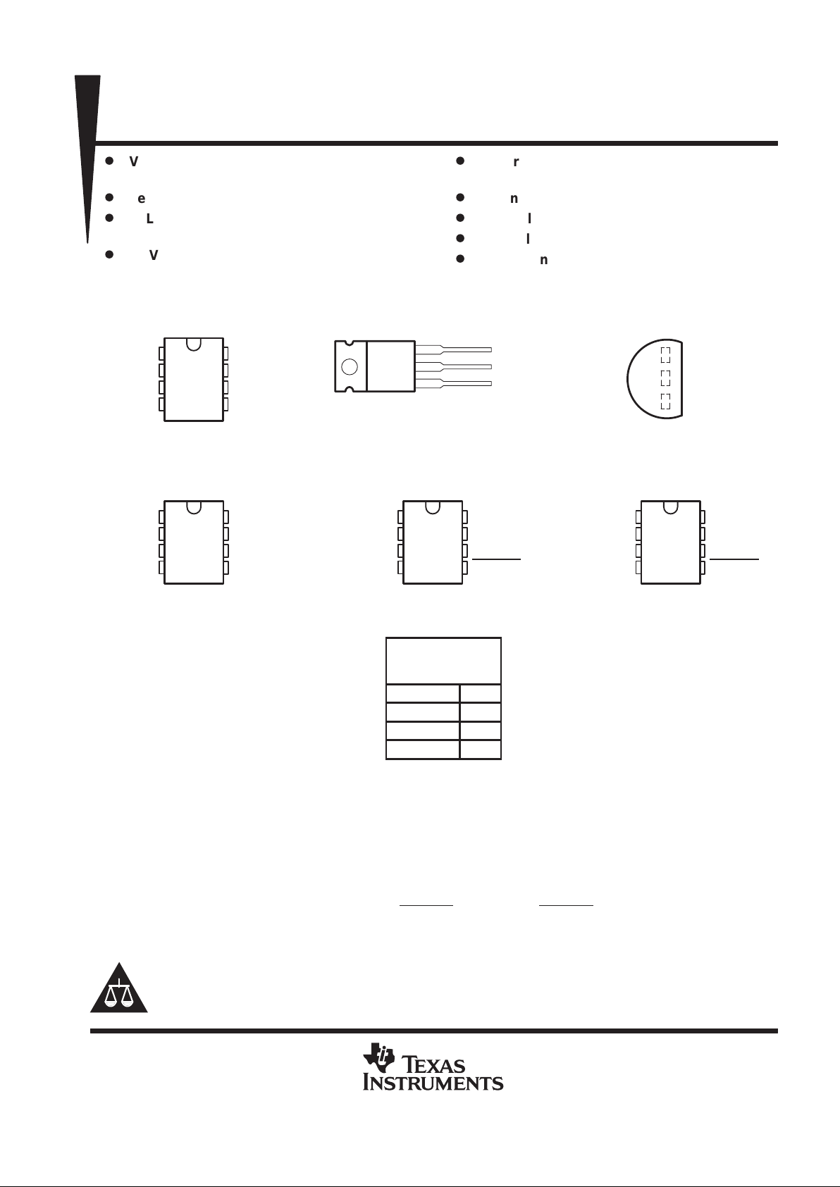
Very Low Dropout Voltage, Less Than 0.6 V
at 150 mA
D
Very Low Quiescent Current
D
TTL- and CMOS-Compatible Enable on
TL751L Series
D
60-V Load-Dump Protection
D
Reverse Transient Protection Down to
–50 V
D
Internal Thermal-Overload Protection
D
Overvoltage Protection
D
Internal Overcurrent-Limiting Circuitry
D
Less Than 500-µA Disable (TL751L Series)
DEVICE
COMPONENT
COUNT
Transistors 20
JFETs 2
Diodes 5
Resistors 16
description
The TL750L and TL751L series are low-dropout positive-voltage regulators specifically designed for
battery-powered systems. These devices incorporate overvoltage and current-limiting protection circuitry,
along with internal reverse-battery protection circuitry to protect the devices and the regulated system. The
series is fully protected against 60-V load-dump and reverse-battery conditions. Extremely low quiescent
current during full-load conditions makes these devices ideal for standby power systems.
The TL750L and TL751L series of fixed-output voltage regulators offers 5-V, 8-V , 10-V, and 12-V options. The
TL751L series has the addition of an enable (ENABLE
) input. When ENABLE is high, the regulator output is
placed in the high-impedance state. This gives the designer complete control over power up, power down, or
emergency shutdown.
Copyright 1999, Texas Instruments Incorporated
PRODUCTION DATA information is current as of publication date.
Products conform to specifications per the terms of Texas Instruments
standard warranty. Production processing does not necessarily include
testing of all parameters.
Please be aware that an important notice concerning availability, standard warranty, and use in critical applications of
Texas Instruments semiconductor products and disclaimers thereto appears at the end of this data sheet.
OUTPUT
NC
NC
NC
INPUT
NC
COMMON
NC
8
7
6
5
OUTPUT
COMMON
COMMON
NC
INPUT
COMMON
COMMON
NC
TL750L ...D PACKAGE
(TOP VIEW)
The common terminal is in electrical
contact with the mounting base.
TO-226AA
TL750L . . . KC PACKAGE
(TOP VIEW)
TL750L . . . LP PACKAGE
(TOP VIEW)
OUTPUT
COMMON
COMMON
NC
INPUT
COMMON
COMMON
ENABLE
OUTPUT
NC
NC
NC
INPUT
NC
COMMON
ENABLE
TL750L ...P PACKAGE
(TOP VIEW)
TL751L ...D PACKAGE
(TOP VIEW)
TL751L ...P PACKAGE
(TOP VIEW)
TO-220AB
1
2
3
4
8
7
6
5
1
2
3
4
8
7
6
5
1
2
3
4
8
7
6
5
1
2
3
4
OUTPUT
COMMON
INPUT
INPUT
COMMON
OUTPUT
NC – No internal connection
TL750L, TL751L SERIES
LOW-DROPOUT VOLTAGE REGULATORS
SLVS017I – SEPTEMBER 1987 – REVISED JULY 1999
2
POST OFFICE BOX 655303 • DALLAS, TEXAS 75265
description (continued)
The TL750LxxC and the TL751LxxC series are characterized for operation over the virtual junction temperature
range of 0°C to 125°C . The TL750L05Q and TL751L05Q are characterized for operation over the virtual
junction temperature range of –40°C to 125°C.
AVAILABLE OPTIONS
PACKAGED DEVICES
T
J
V
O
TYP
AT
25°C
SMALL
OUTLINE
(D)
HEAT-SINK
MOUNTED
(KC)
PLASTIC
CYLINDRICAL
(LP)
PLASTIC
DIP
(P)
CHIP
FORM
(Y)
5 V
TL750L05CD
TL751L05CD
TL750L05CKC TL750L05CLP
TL750L05CP
TL751L05CP
TL750L05Y
°
°
8 V
TL750L08CD
TL751L08CD
TL750L08CKC TL750L08CLP
TL750L08CP
TL751L08CP
TL750L08Y
0°C to 125°C
10 V
TL750L10CD
TL751L10CD
TL750L10CKC TL750L10CLP
TL750L10CP
TL751L10CP
TL750L10Y
12 V
TL750L12CD
TL751L12CD
TL750L12CKC TL750L12CLP
TL750L12CP
TL751L12CP
TL750L12Y
–40°C to 125°C 5 V
TL750L05QD
TL751L05QD
– – – –
The D, KTE, and LP packages are available taped and reeled. The KTP is only available taped and reeled. Add R suffix to
device type (e.g., TL750L05CDR). Chip forms are tested at 25°C.
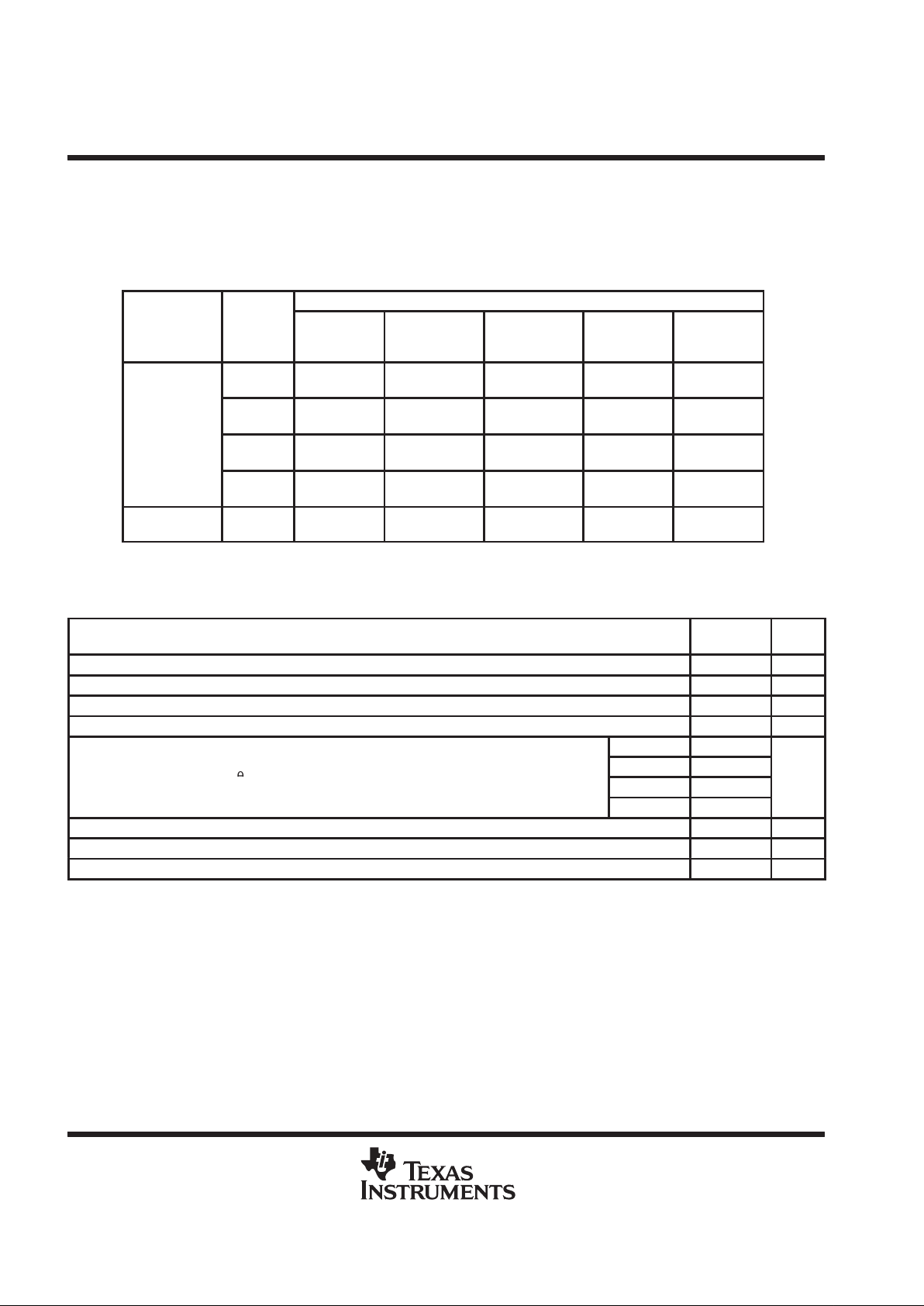
absolute maximum ratings over operating junction temperature range (unless otherwise noted)
†
TL750Lxx
TL751Lxx
UNIT
Continuous input voltage 26 V
Transient input voltage, TA = 25°C (see Note 1) 60 V
Continuous reverse input voltage –15 V
Transient reverse input voltage: t ≤ 100 ms –50 V
D package 97
p
KC package 22
°
Package thermal impedance, θ
JA
(see Notes 2 and 3)
LP package 156
°C
P package 127
Virtual junction temperature range, T
J
–40 to 150 °C
Lead temperature 1,6 mm (1/16 inch) for 10 seconds 260 °C
Storage temperature range, T
stg
–65 to 150 °C
†
Stresses beyond those listed under “absolute maximum ratings” may cause permanent damage to the device. These are stress ratings only, and
functional operation of the device at these or any other conditions beyond those indicated under “recommended operating conditions” is not
implied. Exposure to absolute-maximum-rated conditions for extended periods may affect device reliability.
NOTES: 1. The transient input voltage rating applies to the waveform shown in Figure 1.
2. Maximum power dissipation is a function of TJ(max), θJA, and TA. The maximum allowable power dissipation at any allowable
ambient temperature is PD = (TJ(max) – TA)/θJA. Operating at the absolute maximum TJ of 150°C can impact reliability.
3. The package thermal impedance is calculated in accordance with JESD 51, except for through-hole packages, which use a trace
length of zero.
TL750L, TL751L SERIES
LOW-DROPOUT VOLTAGE REGULATORS
SLVS017I – SEPTEMBER 1987 – REVISED JULY 1999
3
POST OFFICE BOX 655303 • DALLAS, TEXAS 75265
recommended operating conditions over recommended operating junction temperature range
(unless otherwise noted)
MIN MAX UNITS
TL75xL05 6 26
p
TL75xL08 9 26
Input voltage, V
I
TL75xL10 11 26
V
TL75xL12 13 26
High-level ENABLE input voltage, V
IH
TL751Lxx 2 15 V
TA = 25°C TL751Lxx –0.3 0.8
L
ow-level
ENABLE i
nput voltage,
V
IL
†
TA = full range‡TL751Lxx –0.15 0.8
V
Output current range, I
O
TL75xLxx 0 150 mA
p
p
TL75xLxxC 0 125
°
Operating virtual junction temperature, T
J
TL75xL05Q –40 125
°C
†
The algebraic convention, in which the least positive (most negative) value is designated minimum, is used in this data sheet for ENABLE voltage
levels and temperature only.
‡
Full range is 0°C to 125°C for the TL75xLxxC devices, and –40°C to 125°C for the TL75L05Q devices.
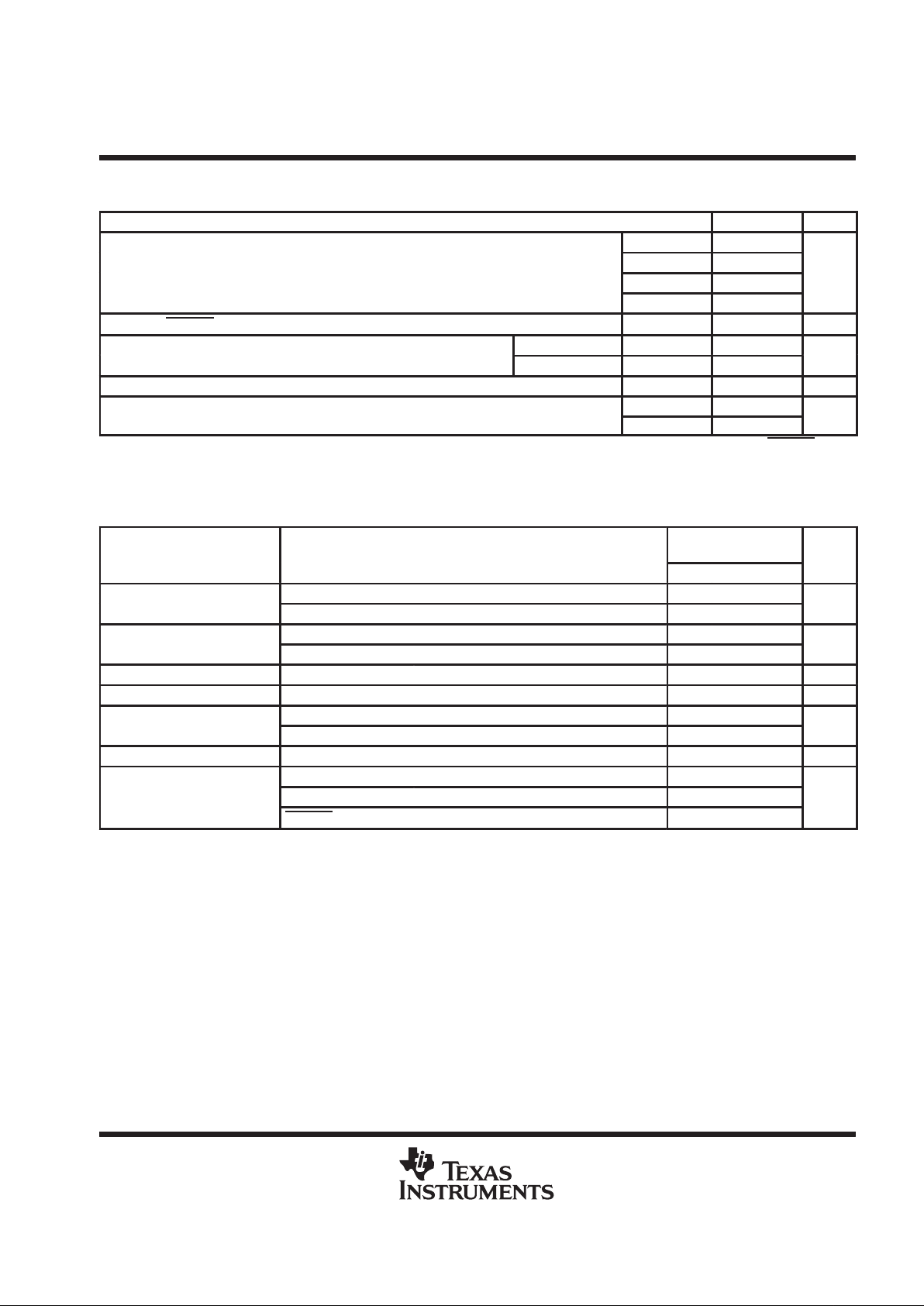
electrical characteristics, V
I
= 14 V, I
O
= 10 mA, TJ = 25°C (unless otherwise noted) (see Note 4)
PARAMETER
TEST CONDITIONS
§
TL750L05
TL751L05
UNIT
MIN TYP MAX
p
4.80 5 5.2
Output voltage
TJ = TJ(min) to 125°C
¶
4.75 5.25
V
p
VI = 9 V to 16 V 5 10
Input regulation voltage
VI = 6 V to 26 V 6 30
mV
Ripple rejection VI = 8 V to 18 V, f = 120 Hz 60 65 dB
Output regulation voltage IO = 5 mA to 150 mA 20 50 mV
p
IO = 10 mA 0.2
Dropout voltage
IO = 150 mA 0.6
V
Output noise voltage f = 10 Hz to 100 kHz 500 µV
IO = 150 mA 10 12
Input bias current
VI = 6 V to 26 V, IO = 10 mA, TJ = TJ(min) to 125°C
¶
1 2
mA
ENABLE > 2 V
0.5
§
Pulse-testing techniques are used to maintain the junction temperature as close to the ambient temperature as possible. Thermal effects must
be taken into account separately. All characteristics are measured with a 0.1-µF capacitor across the input and a 10-µF capacitor , with equivalent
series resistance of less than 0.4 Ω, across the output.
¶
TJ(min) is 0°C for the TL75xLxxC devices, and –40°C for the TL75xLxxQ devices.
NOTE 4: For TL750L05Q/TL751L05Q, all characteristics are measured with a 0.1-µF tantalum capacitor on the output with equivalent series
resistance within the guidelines shown in Figure 4.

TL750L, TL751L SERIES
LOW-DROPOUT VOLTAGE REGULATORS
SLVS017I – SEPTEMBER 1987 – REVISED JULY 1999
4
POST OFFICE BOX 655303 • DALLAS, TEXAS 75265
electrical characteristics, V
I
= 14 V, IO = 10 mA, TJ = 25°C (unless otherwise noted)
PARAMETER
TEST CONDITIONS
†
TL750L08
TL751L08
UNIT
MIN TYP MAX
p
7.68 8 8.32
Output voltage
TJ = 0°C to 125°C 7.6 8.4
V
p
VI = 10 V to 17 V 10 20
Input regulation voltage
VI = 9 V to 26 V 25 50
mV
Ripple rejection VI = 11 V to 21 V, f = 120 Hz 60 65 dB
Output regulation voltage IO = 5 mA to 150 mA 40 80 mV
p
IO = 10 mA 0.2
Dropout voltage
IO = 150 mA 0.6
V
Output noise voltage f = 10 Hz to 100 kHz 500 µV
IO = 150 mA 10 12
Input bias current
VI = 9 V to 26 V, IO = 10 mA, TJ = 0°C to 125°C 1 2
mA
ENABLE > 2 V
0.5
†
Pulse-testing techniques are used to maintain the junction temperature as close to the ambient temperature as possible. Thermal effects must
be taken into account separately. All characteristics are measured with a 0.1-µF capacitor across the input and a 10-µF capacitor , with equivalent
series resistance of less than 0.4 Ω, across the output.
electrical characteristics, V
I
= 14 V, I
O
= 10 mA, TJ = 25°C (unless otherwise noted)
PARAMETER
TEST CONDITIONS
†
TL750L10
TL751L10
UNIT
MIN TYP MAX
p
9.6 10 10.4
Output voltage
TJ = 0°C to 125°C 9.5 10.5
V
p
VI = 12 V to 19 V 10 25
Input regulation voltage
VI = 11 V to 26 V 30 60
mV
Ripple rejection VI = 12 V to 22 V, f = 120 Hz 60 65 dB
Output regulation voltage IO = 5 mA to 150 mA 50 100 mV
p
IO = 10 mA 0.2
Dropout voltage
IO = 150 mA 0.6
V
Output noise voltage f = 10 Hz to 100 kHz 700 µV
IO = 150 mA 10 12
Input bias current
VI = 11 V to 26 V, IO = 10 mA, TJ = 0°C to 125°C 1 2
mA
ENABLE > 2 V
0.5
†
Pulse-testing techniques are used to maintain the junction temperature as close to the ambient temperature as possible. Thermal effects must
be taken into account separately. All characteristics are measured with a 0.1-µF capacitor across the input and a 10-µF capacitor , with equivalent
series resistance of less than 0.4 Ω, across the output.

TL750L, TL751L SERIES
LOW-DROPOUT VOLTAGE REGULATORS
SLVS017I – SEPTEMBER 1987 – REVISED JULY 1999
5
POST OFFICE BOX 655303 • DALLAS, TEXAS 75265
electrical characteristics, V
I
= 14 V, IO = 10 mA, TJ = 25°C (unless otherwise noted)
PARAMETER
TEST CONDITIONS
†
TL750L12
TL751L12
UNIT
MIN TYP MAX
p
11.52 12 12.48
Output voltage
TJ = 0°C to 125°C 11.4 12.6
V
p
VI = 14 V to 19 V 15 30
Input regulation voltage
VI = 13 V to 26 V 20 40
mV
Ripple rejection VI = 13 V to 23 V, f = 120 Hz 50 55 dB
Output regulation voltage IO = 5 mA to 150 mA 50 120 mV
p
IO = 10 mA 0.2
Dropout voltage
IO = 150 mA 0.6
V
Output noise voltage f = 10 Hz to 100 kHz 700 µV
IO = 150 mA 10 12
Input bias current
VI = 13 V to 26 V, IO = 10 mA, TJ = 0°C to 125°C 1 2
mA
ENABLE > 2 V
0.5
†
Pulse-testing techniques are used to maintain the junction temperature as close to the ambient temperature as possible. Thermal effects must
be taken into account separately. All characteristics are measured with a 0.1-µF capacitor across the input and a 10-µF capacitor , with equivalent
series resistance of less than 0.4 Ω, across the output.
electrical characteristics, V
I
= 14 V, IO = 10 mA, TJ = 25°C (unless otherwise noted)
TL750L05Y
PARAMETER
TEST CONDITIONS
†
MIN TYP MAX
UNIT
Output voltage 5 V
p
VI = 9 V to 16 V 5
Input regulation voltage
VI = 6 V to 26 V 6
mV
Ripple rejection VI = 8 V to 18 V, f = 120 Hz 65 dB
Output regulation voltage IO = 5 mA to 150 mA 20 mV
Output noise voltage f = 10 Hz to 100 kHz 500 µV
p
IO = 150 mA 10
Input bias current
VI = 6 V to 26 V, IO = 10 mA 1
mA
†
Pulse-testing techniques are used to maintain the junction temperature as close to the ambient temperature as possible. Thermal effects must
be taken into account separately. All characteristics are measured with a 0.1-µF capacitor across the input and a 10-µF capacitor , with equivalent
series resistance of less than 0.4 Ω, across the output.

TL750L, TL751L SERIES
LOW-DROPOUT VOLTAGE REGULATORS
SLVS017I – SEPTEMBER 1987 – REVISED JULY 1999
6
POST OFFICE BOX 655303 • DALLAS, TEXAS 75265
electrical characteristics, V
I
= 14 V, IO = 10 mA, TJ = 25°C (unless otherwise noted)
TL750L08Y
PARAMETER
TEST CONDITIONS
†
MIN TYP MAX
UNIT
Output voltage 8 V
p
VI = 10 V to 17 V 10
Input regulation voltage
VI = 9 V to 26 V 25
mV
Ripple rejection VI = 11 V to 21 V, f = 120 Hz 65 dB
Output regulation voltage IO = 5 mA to 150 mA 40 mV
Output noise voltage f = 10 Hz to 100 kHz 500 µV
p
IO = 150 mA 10
Input bias current
VI = 9 V to 26 V, IO = 10 mA 1
mA
†
Pulse-testing techniques are used to maintain the junction temperature as close to the ambient temperature as possible. Thermal effects must
be taken into account separately. All characteristics are measured with a 0.1-µF capacitor across the input and a 10-µF capacitor , with equivalent
series resistance of less than 0.4 Ω, across the output.
electrical characteristics, V
I
= 14 V, I
O
= 10 mA, TJ = 25°C (unless otherwise noted)
TL750L10Y
PARAMETER
TEST CONDITIONS
†
MIN TYP MAX
UNIT
Output voltage 10 V
p
VI = 12 V to 19 V 10
Input regulation voltage
VI = 11 V to 26 V 30
mV
Ripple rejection VI = 12 V to 22 V, f = 120 Hz 65 dB
Output regulation voltage IO = 5 mA to 150 mA 50 mV
Output noise voltage f = 10 Hz to 100 kHz 700 µV
p
IO = 150 mA 10
Input bias current
VI = 11 V to 26 V, IO = 10 mA 1
mA
†
Pulse-testing techniques are used to maintain the junction temperature as close to the ambient temperature as possible. Thermal effects must
be taken into account separately. All characteristics are measured with a 0.1-µF capacitor across the input and a 10-µF capacitor , with equivalent
series resistance of less than 0.4 Ω, across the output.
electrical characteristics, V
I
= 14 V, I
O
= 10 mA, TJ = 25°C (unless otherwise noted)
TL750L12Y
PARAMETER
TEST CONDITIONS
†
MIN TYP MAX
UNIT
Output voltage 12 V
p
VI = 14 V to 19 V 15
Input regulation voltage
VI = 13 V to 26 V 20
mV
Ripple rejection VI = 13 V to 23 V, f = 120 Hz 55 dB
Output regulation voltage IO = 5 mA to 150 mA 50 mV
Output noise voltage f = 10 Hz to 100 kHz 700 µV
p
IO = 150 mA 10
Input bias current
VI = 13 V to 26 V, IO = 10 mA 1
mA
†
Pulse-testing techniques are used to maintain the junction temperature as close to the ambient temperature as possible. Thermal effects must
be taken into account separately. All characteristics are measured with a 0.1-µF capacitor across the input and a 10-µF capacitor , with equivalent
series resistance of less than 0.4 Ω, across the output.

TL750L, TL751L SERIES
LOW-DROPOUT VOLTAGE REGULATORS
SLVS017I – SEPTEMBER 1987 – REVISED JULY 1999
7
POST OFFICE BOX 655303 • DALLAS, TEXAS 75265
TYPICAL CHARACTERISTICS
30
20
0 100 200
40
TRANSIENT INPUT VOLTAGE
vs
TIME
60
300 400 500
600
i
V – Transient Input Voltage – V
0
10
50
tr = 1 ms
TA = 25°C
VI = 14 V + 46e
(–t/0.230)
for t ≥ 5 ms
t – Time – ms
Figure 1 Figure 2
20
15
5
0
0123
– Input Current – mA
25
35
40
456
30
10
VI – Input Voltage – V
TL750L05
INPUT CURRENT
vs
INPUT VOLTAGE
I
I
30
20
10
0
024
40
50
60
68 12
1410
VI – Input Voltage – V
TL750L12
INPUT CURRENT
vs
INPUT VOLTAGE
– Input Current – mAI
I
Figure 3

TL750L, TL751L SERIES
LOW-DROPOUT VOLTAGE REGULATORS
SLVS017I – SEPTEMBER 1987 – REVISED JULY 1999
8
POST OFFICE BOX 655303 • DALLAS, TEXAS 75265
TYPICAL CHARACTERISTICS
IL – Load Current – mA
TL750L05
EQUIVALENT SERIES RESISTANCE
vs
LOAD CURRENT
0.2
0.1
0
010
ESR – Equivalent Series Resistance –
0.3
0.4
0.5
0.024
0.6
0.7
0.8
0.9
1.0
Region of Best Stability
80 120 150
Potential Instability Region
CL = 10-µF Tantalum Capacitor
TA = –40°C to 125°C
Potential Instability Region
Ω
Figure 4

IMPORTANT NOTICE
T exas Instruments and its subsidiaries (TI) reserve the right to make changes to their products or to discontinue
any product or service without notice, and advise customers to obtain the latest version of relevant information
to verify, before placing orders, that information being relied on is current and complete. All products are sold
subject to the terms and conditions of sale supplied at the time of order acknowledgement, including those
pertaining to warranty, patent infringement, and limitation of liability.
TI warrants performance of its semiconductor products to the specifications applicable at the time of sale in
accordance with TI’s standard warranty. Testing and other quality control techniques are utilized to the extent
TI deems necessary to support this warranty. Specific testing of all parameters of each device is not necessarily
performed, except those mandated by government requirements.
CERT AIN APPLICATIONS USING SEMICONDUCTOR PRODUCTS MAY INVOLVE POTENTIAL RISKS OF
DEATH, PERSONAL INJURY, OR SEVERE PROPERTY OR ENVIRONMENTAL DAMAGE (“CRITICAL
APPLICATIONS”). TI SEMICONDUCTOR PRODUCTS ARE NOT DESIGNED, AUTHORIZED, OR
WARRANTED TO BE SUITABLE FOR USE IN LIFE-SUPPORT DEVICES OR SYSTEMS OR OTHER
CRITICAL APPLICATIONS. INCLUSION OF TI PRODUCTS IN SUCH APPLICA TIONS IS UNDERSTOOD T O
BE FULLY AT THE CUSTOMER’S RISK.
In order to minimize risks associated with the customer’s applications, adequate design and operating
safeguards must be provided by the customer to minimize inherent or procedural hazards.
TI assumes no liability for applications assistance or customer product design. TI does not warrant or represent
that any license, either express or implied, is granted under any patent right, copyright, mask work right, or other
intellectual property right of TI covering or relating to any combination, machine, or process in which such
semiconductor products or services might be or are used. TI’s publication of information regarding any third
party’s products or services does not constitute TI’s approval, warranty or endorsement thereof.
Copyright 1999, Texas Instruments Incorporated
 Loading...