

T
TL5632C
8-BIT 3-CHANNEL HIGH-SPEED DIGITAL-TO-ANALOG CONVERTER
SLAS091 – DECEMBER 1994
D
8-Bit Resolution
D
Linearity . . . ±1/2 LSB Maximum
D
Differential Nonlinearity...±1/2 LSB
Maximum
D
Conversion Rate...60 MHz Min
D
Nominal Output Signal Operating Range
V
to VCC – 1 V
CC
D
TTL Digital Input Voltage
D
5-V Single Power Supply Operation
D
Low Power Consumption...350 mW Typ
description
The TL5632C is a low-power ultra-high-speed
video digital-to-analog converter that uses the
Advanced Low-Power Schottky (ALS) process.
The device has a three channel I/O; the red, the
blue, and the green channel. The red, blue, and
green signals are referred to collectively as the
RGB signal. An internally generated reference is
also provided for the standard video output
voltage range. Conversion of digital signals to
analog signals can be at a sampling rate of dc to
60 MHz. The high conversion rate makes the
TL5632C suitable for digital television, computer
digital video processing, and high-speed data
conversion.
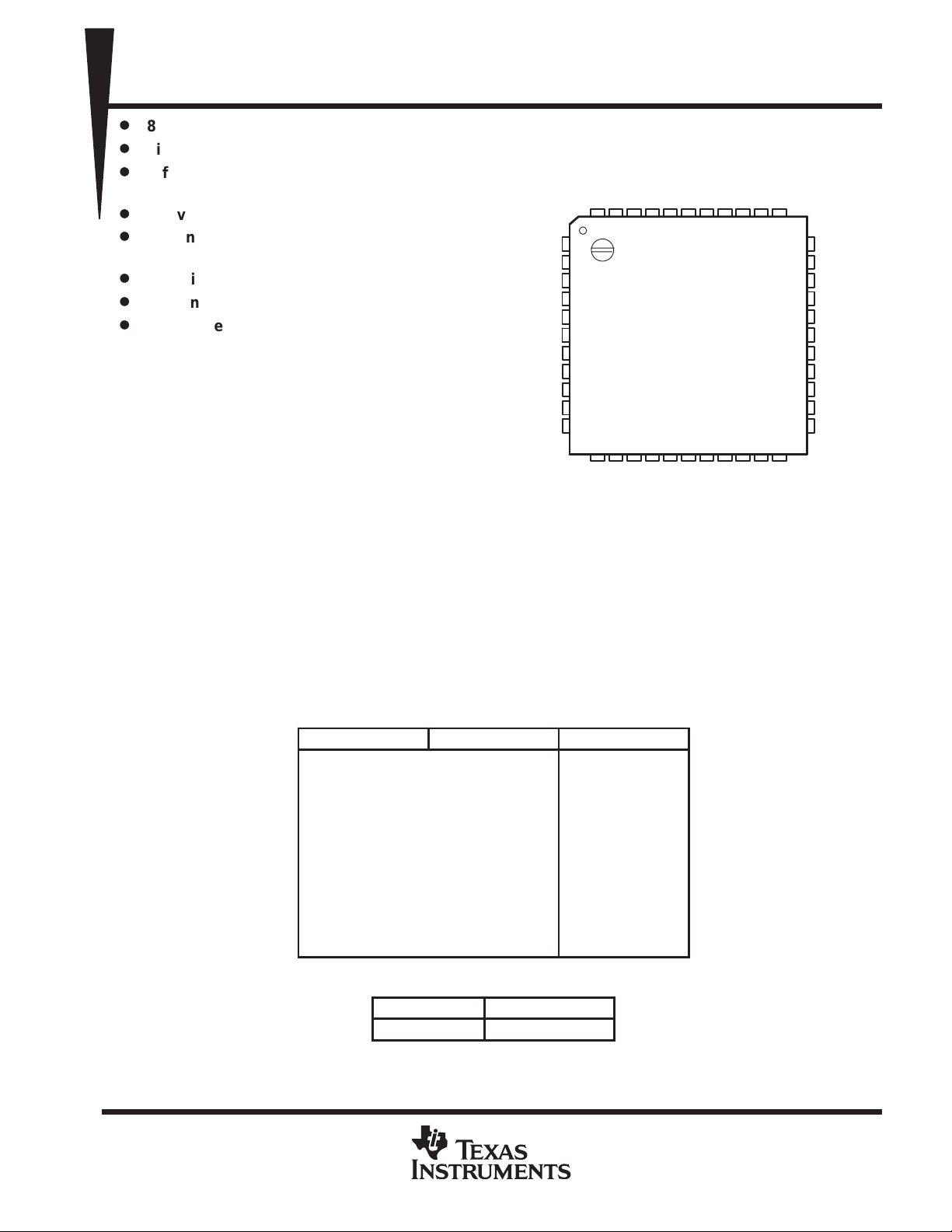
DVCCAVCCR
NC
43 42 41 40 3944 38
(MSB) R
(LSB) R
(MSB) G
NC – No internal connection
1
1
R
2
2
R
3
3
4
R
4
5
R
5
6
R
6
7
R
7
8
8
9
1
10
G
2
11
G
3
12 13
4
G
14 15 16 17
G5G6G
FR PACKAGE
(TOP VIEW)
OUT
OUT
GND
GND
7
G
18 19 20 21 22
8
B1B2B3B4B
G
NC
(LSB)
(MSB)
GND
B
36 35 3437
OUT
GND
REF IN
33
32
31
30
29
28
27
26
25
24
23
5
REF OU
AV
CC
C
COMP
DV
CC
GND
IN
CLK
R
IN
CLK
G
CLK
IN
B
(LSB)
B
8
B
7
B
6
The TL5632C is characterized for operation from
0°C to 70°C.
FUNCTION TABLE
STEP
0
1
•
•
•
127
128
129
•
•
•
254
255
0°C to 70°C TL5632CFR
DIGITAL INPUT OUTPUT VOLTAGE
L L L L L L L L
L L L L L L L H
L H H H H H H H
H L L L L L L L
H L L L L L L H
H H H H H H H L
H H H H H H H H
AVAILABLE OPTIONS
T
A
•
•
•
•
•
•
3.980 V
3.984 V
•
•
•
4.488 V
4.492 V
4.996 V
•
•
•
4.996 V
5.000 V
PACKAGE
PRODUCTION DATA information is current as of publication date.
Products conform to specifications per the terms of Texas Instruments
standard warranty. Production processing does not necessarily include
testing of all parameters.
POST OFFICE BOX 655303 • DALLAS, TEXAS 75265
Copyright 1994, Texas Instruments Incorporated
1
TL5632C
8-BIT 3-CHANNEL HIGH-SPEED DIGITAL-TO-ANALOG CONVERTER
SLAS091 – DECEMBER 1994
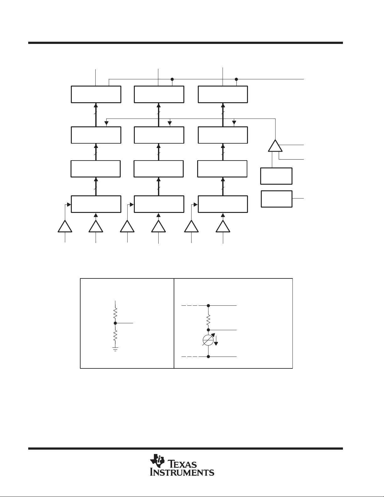
functional block diagram
R
OUT
Resistor Network
(R)
88
Current Switch
(R)
88 8
Buffer (R) Buffer (G) Buffer (B)
88 8
Master-Slave
Register (R)
G
OUT
Resistor Network
(G)
Current Switch
(G)
Master-Slave
Register (G)
Resistor Network
Current Switch
Master-Slave
Register (B)
B
OUT
(B)
(B)
AV
CC
8
C
COMP
REF IN
Reference
Resistor
Reference
Voltage
REF OUT
CLKR IN R1–R8 G1–G8 B1–B8
schematics of outputs
EQUIVALENT OF REF OUT EQUIVALENT OF R
CLKG IN CLKB IN
AV
CC
1 kΩ
REF OUT
4 kΩ
OUT
240 Ω typical
, G
AV
R
OUT
GND
CC
OUT
, G
, B
OUT
OUT
, B
OUT
2
POST OFFICE BOX 655303 • DALLAS, TEXAS 75265
I/O
DESCRIPTION
TL5632C
8-BIT 3-CHANNEL HIGH-SPEED DIGITAL-TO-ANALOG CONVERTER
SLAS091 – DECEMBER 1994
Terminal Functions
TERMINAL
NAME NO.
B1 – B
8
B
OUT
C
COMP
CLKB IN 26 I B-channel clock input
CLKG IN 27 I G-channel clock input
CLKR IN 28 I R-channel clock input
G1 – G
8
GND 29, 35, 37,
G
OUT
NC 17, 44 No connection internally
R1 – R
8
R
OUT
AV
CC
DV
CC
REF IN 34 I Reference voltage input. REF IN accepts the reference voltage on REF OUT. An external reference can
REF OUT 33 O Reference voltage output. An internal voltage divider generates the voltage level (see schematics of
NOTE 1: VCC – V
18 – 25 I B-channel digital input (B1= MSB)
36 O B-channel analog output
31 Phase compensation capacitance. A 1 µF capacitor is connected from C
9 – 16 I G-Channel digital input (G1= MSB)
39, 41
38 O G-channel analog output
1 – 8 I R-channel digital input (R1= MSB)
40 O R-channel analog output
32, 42 Analog power supply voltage
30, 43 Digital power supply voltage
≤ 1.2 V
ref
Ground. All GND terminals are connected internally; however, all GND terminals should be connected
externally to a ground plane or equivalent low impedance ground return.
also be applied consistent with Note 1.
outputs, page 2).
COMP
to GND.
absolute maximum ratings over operating free-air temperature range (unless otherwise noted)
Power supply voltage range, AV
Digital input voltage range,V
Analog output voltage range, R
Reference input range, REF IN –0.3 V to AV
Reference output range, REF OUT –0.3 V to AV
Operating free-air temperature range, T
Storage temperature range –65°C to 150°C. . . . . . . . . . . . . . . . . . . . . . . . . . . . . . . . . . . . . . . . . . . . . . . . . . . . . . . .
Lead temperature 1,6 mm (1/16 inch) from case for 10 seconds 260°C. . . . . . . . . . . . . . . . . . . . . . . . . . . . . . .
†
Stresses beyond those listed under “absolute maximum ratings” may cause permanent damage to the device. These are stress ratings only, and
functional operation of the device at these or any other conditions beyond those indicated under “recommended operating conditions” is not
implied. Exposure to absolute-maximum-rated conditions for extended periods may affect device reliability.
NOTE 2: All voltage values are with respect to GND.
, DVCC (see Note 2) –0.3 V to 7 V. . . . . . . . . . . . . . . . . . . . . . . . . . . . . . . . .
CC
–0.3 V to DV
. . . . . . . . . . . . . . . . . . . . . . . . . . . . . . . . . . . . . . . . . . . . . . . . . . . . . .
I
OUT
, G
, B
OUT
0°C to 70°C. . . . . . . . . . . . . . . . . . . . . . . . . . . . . . . . . . . . . . . . . . . . . .
A
OUT
, C
(externally applied) –0.3 V to AVCC + 0.3 V. . . .
COMP
CC
CC
+ 0.3 V. . . . . . . . . . . . . . . . . . . . . . . . . . . . . . . . . . . . . . . . . . . . .
+ 0.3 V. . . . . . . . . . . . . . . . . . . . . . . . . . . . . . . . . . . . . . . . . .
†
CC
POST OFFICE BOX 655303 • DALLAS, TEXAS 75265
3

TL5632C
ns
T
25°C
C
≤ 5 pF
‡
ns
8-BIT 3-CHANNEL HIGH-SPEED DIGITAL-TO-ANALOG CONVERTER
SLAS091 – DECEMBER 1994
recommended operating conditions
MIN NOM MAX UNIT
Supply voltage, AVCC, DV
High-level input voltage, V
Low-level input voltage, V
Reference voltage, V
Setup time, data before CLK↑, t
Hold time, data after CLK↑, t
Pulse duration at high level, t
Pulse duration at low level, t
External phase compensation capacitance, C
Operating free-air temperature, T
NOTE 1: VCC – V
CC
IH
IL
(see Note 1) 3.8 4 4.2 V
ref
su1
h1
w1
w2
COMP
A
≤ 1.2 V
ref
electrical characteristics over recommended ranges of supply voltage and operating free-air
temperature (unless otherwise noted)
PARAMETER TEST CONDITIONS MIN TYP
Resolution 8 Bit
I
I
I
V
V
V
z
I
IH
IL
ref
ref
FS
ZS
o
CC
High-level input current VCC = 5.25 V, VIH = 2.7 V 20 µA
Low-level input current VCC = 5.25 V, VIH = 2.7 V –400 µA
Reference input current REF IN = 4 V 10 µA
Reference output voltage VCC = 5 V, With internal reference 3.8 4 4.2 V
Full-scale analog output voltage VIH = 2 V, REF IN = 4 V AVCC–15 AV
Zero-scale analog output voltage VIL = 0.8 V, REF IN = 4 V 3.9 3.98 4.05 V
RGB full-scale ratio 0% 4% 8%
Output impedance 200 240 280 W
Supply current 70 90 mA
4.75 5 5.25 V
2 V
0.8 V
10 ns
3 ns
8.3 ns
8.3 ns
1 µF
0 70 °C
†
MAX UNIT
CCAVCC
+15 mV
operating characteristics over recommended ranges of supply voltage and operating free-air
temperature (unless otherwise noted)
PARAMETER TEST CONDITIONS MIN TYP†MAX UNIT
E
L
E
D
f
c
t
PLH
t
PHL
t
r
t
f
†
All typical values are at VCC = 5 V, TA = 25°C.
‡
CL includes probe and jig capacitances.
Linearity error End point, REF IN = 4 V ±0.5 LSB
Differential linearity error REF IN = 4 V ±0.5 LSB
Maximum conversion rate 60 MHz
Propagation delay time, low-to-high level
Propagation delay time, high-to-low level
Rise time
Fall time 5
°
,
=
A
p
L
10
10
5
4
POST OFFICE BOX 655303 • DALLAS, TEXAS 75265

TL5632C
8-BIT 3-CHANNEL HIGH-SPEED DIGITAL-TO-ANALOG CONVERTER
SLAS091 – DECEMBER 1994
PARAMETER MEASUREMENT INFORMATION
CLKR IN, CLKG IN, CLKB IN
R1–R8, G1–G8, B1–B
R
OUT
(Analog Output)
5
4.996
•
•
•
4.496
4.492
4.488
•
•
•
– Analog Output Voltage – V
3.988
O
V
3.984
3.980
LSB
(Clock)
(Input Data)
, G
, B
OUT
OUT
t
w1
t
su1
8
t
PLH
t
h1
t
r
10% 10%
t
w2
1.5 V
t
f
90% 90%
50% 50%
t
PHL
1.5 V
3 V
0
3 V
0
V
V
FS
ZS
TYPICAL CHARACTERISTICS
V
FS
EL 254
↓
EL 128
↓
EL 127
↓
– Analog Output Voltage – VV
O
V
↓
EL 1
↑
ZS
EL 2
↑
↑
↑
↓
EL 129
↑
↓
↑
••• •••
MSB
00000000
00000001
00000010
Digital Input Code
01111111
10000000
10000001
Figure 1. Ideal Conversion Characteristics
11111111
11111110
00000000
00000001
Figure 2. End-Point Linearity Error
POST OFFICE BOX 655303 • DALLAS, TEXAS 75265
••• •••
00000010
01111111
10000000
Digital Input Code
10000001
11111110
11111111
5

TL5632C
8-BIT 3-CHANNEL HIGH-SPEED DIGITAL-TO-ANALOG CONVERTER
SLAS091 – DECEMBER 1994
APPLICATION INFORMATION
The following design procedures should be used for optimum operation.
D
External analog and digital circuitry should be physically separated and shielded as much as possible to
reduce system noise.
D
RF breadboarding or RF printed-circuit-board (PCB) techniques should be used throughout the evaluation
and production process.
D
Wide ground leads or a ground plane should be used on the PCB layouts to minimize parasitic inductance
and resistance. A ground plane is the better choice for noise reduction.
D
AVCC and DVCC are also separate internally , so they must be connected externally. These external PCB
leads should also be made as wide as possible. A ferrite bead or equivalent inductance should be placed
in series with A V
on the board. It is critical that the supply voltage applied to A V
Ripple and noise rejection should be a minimum of 60 dB below the full-scale output range of 1 V
peak-to-peak.
D
AVCC to GND and DVCC to GND should be decoupled with 3.3-µF and 0.1-µF capacitors, respectively , as
close as possible to the appropriate device terminals. A ceramic chip capacitor is recommended for the
0.1-µF capacitor.
and the decoupling capacitor before the A VCC and DVCC leads are connected together
CC
be as noise free and ripple free as possible.
CC
D
The phase compensation capacitor should be connected between C
as possible.
D
The no-connection (NC) terminals on the small-outline package should be connected to GND.
D
AVCC, DVCC, and R
CLK
IN ,and CLKB IN and the input data terminals. GND traces should be placed on both sides of the R
G
G
, and B
OUT
be as short as possible.
OUT
, G
OUT
traces on the PCB to the following signal processing stage. These output traces should
OUT
, and B
should be shielded from the high-frequency terminals CLKR IN,
OUT
and GND with as short a lead-in
COMP
OUT
,
6
POST OFFICE BOX 655303 • DALLAS, TEXAS 75265

TL5632C
8-BIT 3-CHANNEL HIGH-SPEED DIGITAL-TO-ANALOG CONVERTER
SLAS091 – DECEMBER 1994
APPLICATION INFORMATION
DV
CC
AV
CC
88
Buffer
88
Buffer
3.3 µF3.3 µF
0.1 µF
1
2
3
4
5
6
7
8
9
10
11
0.1 µF
R1(MSB)
R
2
R
3
R
4
R
5
R
6
R
7
R8(LSB)
G1(MSB)
G
2
G
3
43 42 41 40 3944 38
NC
CCAVCC
GND
DV
TL5632C
G4G5G6G
12 13
7
14 15 16 17
36 35 3437
GND
GND
OUTGOUTBOUT
R
REF OUT
(LSB)
(MSB)
8
1
B
G
B2B3B4B
NC
18 19 20 21 22
GND
REF IN
AV
CC
C
COMP
DV
CC
GND
CLKR IN
CLKG IN
CLKB IN
(LSB)B
B
B
5
0.1 µF
33
32
31
30
29
28
27
26
25
8
24
7
23
6
3
0.1 µF
C
C
R
C
C
1 µF
G
B
OUT
OUT
OUT
0.1 µF
C
C
88
Buffer
3
Buffer
NOTES: A. Buffers are SN74AS244 or equivalent.
B. 0.1 µF capacitors should be placed as close to the device terminals as possible.
C. The coupling capacitor (CC) value is application specific and selectable by the user.
Figure 3. Typical Bypass, Buffer, and Output Configuration
POST OFFICE BOX 655303 • DALLAS, TEXAS 75265
7

TL5632C
8-BIT 3-CHANNEL HIGH-SPEED DIGITAL-TO-ANALOG CONVERTER
SLAS091 – DECEMBER 1994
MECHANICAL DATA
FR/S-PQFP-G44 PLASTIC QUAD FLATPACK
33 23
34
44
2,25 MAX
22
12
111
8,00 TYP
10,20
SQ
9,80
12,80
SQ
12,00
0,80 TYP
0,40
0,20
0,10 MIN
Seating Plane
0,20
0,10
0°–10°
0,80
0,30
NOTES: A. All linear dimensions are in millimeters.
B. This drawing is subject to change without notice.
8
0,10
4040159/A–10/93
POST OFFICE BOX 655303 • DALLAS, TEXAS 75265

IMPORTANT NOTICE
T exas Instruments and its subsidiaries (TI) reserve the right to make changes to their products or to discontinue
any product or service without notice, and advise customers to obtain the latest version of relevant information
to verify, before placing orders, that information being relied on is current and complete. All products are sold
subject to the terms and conditions of sale supplied at the time of order acknowledgement, including those
pertaining to warranty, patent infringement, and limitation of liability.
TI warrants performance of its semiconductor products to the specifications applicable at the time of sale in
accordance with TI’s standard warranty. Testing and other quality control techniques are utilized to the extent
TI deems necessary to support this warranty . Specific testing of all parameters of each device is not necessarily
performed, except those mandated by government requirements.
CERT AIN APPLICATIONS USING SEMICONDUCTOR PRODUCTS MAY INVOLVE POTENTIAL RISKS OF
DEATH, PERSONAL INJURY, OR SEVERE PROPERTY OR ENVIRONMENTAL DAMAGE (“CRITICAL
APPLICATIONS”). TI SEMICONDUCTOR PRODUCTS ARE NOT DESIGNED, AUTHORIZED, OR
WARRANTED TO BE SUITABLE FOR USE IN LIFE-SUPPORT DEVICES OR SYSTEMS OR OTHER
CRITICAL APPLICA TIONS. INCLUSION OF TI PRODUCTS IN SUCH APPLICATIONS IS UNDERST OOD TO
BE FULLY AT THE CUSTOMER’S RISK.
In order to minimize risks associated with the customer’s applications, adequate design and operating
safeguards must be provided by the customer to minimize inherent or procedural hazards.
TI assumes no liability for applications assistance or customer product design. TI does not warrant or represent
that any license, either express or implied, is granted under any patent right, copyright, mask work right, or other
intellectual property right of TI covering or relating to any combination, machine, or process in which such
semiconductor products or services might be or are used. TI’s publication of information regarding any third
party’s products or services does not constitute TI’s approval, warranty or endorsement thereof.
Copyright 1998, Texas Instruments Incorporated
 Loading...