

TL5501
6-BIT ANALOG-TO-DIGITAL CONVERTER
SLAS026 – OCTOBER 1989 – REVISED APRIL 1990
1
POST OFFICE BOX 655303 • DALLAS, TEXAS 75265
D
6-Bit Resolution
D
Linearity Error... ±0.8%
D
Maximum Conversion Rate...30 MHz Typ
D
Analog Input Voltage Range
V
CC
to VCC – 2 V
D
Analog Input Dynamic Range...1 V
D
TTL Digital I/O Level
D
Low Power Consumption
200 mW Typ
D
5-V Single-Supply Operation
D
Interchangeable With Fujitsu MB40576
description
The TL5501 is a low-power ultra-high-speed video-band analog-to-digital converter that uses the Advanced
Low-Power Schottky (ALS) process. It utilizes the full-parallel comparison (flash method) for high-speed
conversion. It converts wide-band analog signals (such as a video signal) to a digital signal at a sampling rate
of dc to 30 MHz. Because of this high-speed capability , the TL5501 is suitable for digital video applications such
as digital TV, video processing with a computer, or radar signal processing.
The TL5501 is characterized for operation from 0°C to 70°C.
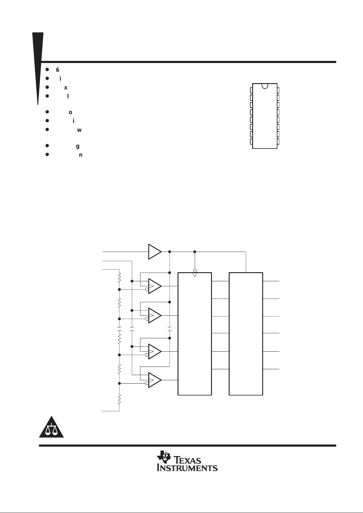
functional block diagram
D0 (LSB)
D1
D2
D3
D4
D5 (MSB)
EN
Latch
and
Buffer
63-to-6
Encoder
CLK
ANLG INPUT
REFT
REFB
63
62
2
1
R
R
R
R
R
Copyright 1990, Texas Instruments Incorporated
PRODUCTION DATA information is current as of publication date.
Products conform to specifications per the terms of Texas Instruments
standard warranty. Production processing does not necessarily include
testing of all parameters.
Please be aware that an important notice concerning availability, standard warranty, and use in critical applications of
Texas Instruments semiconductor products and disclaimers thereto appears at the end of this data sheet.
1
2
3
4
5
6
7
8
16
15
14
13
12
11
10
9
(LSB) D0
D1
D2
D3
D4
(MSB) D5
CLK
GND
GND
DGTL V
CC
ANLG V
CC
REFB
ANLG INPUT
REFT
ANLG V
CC
DGTL V
CC
N PACKAGE
(TOP VIEW)
TL5501
6-BIT ANALOG-TO-DIGITAL CONVERTER
SLAS026 – OCTOBER 1989 – REVISED APRIL 1990
2
POST OFFICE BOX 655303 • DALLAS, TEXAS 75265
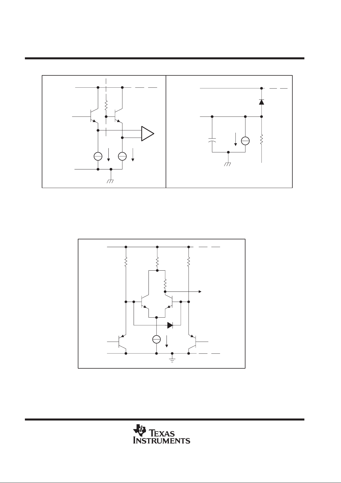
equivalents of analog input circuit
ANLG V
CC
V
I
D
r
i
V
refB
(see Note A)
C
i
I
bias
ANLG GND
ANLG V
CC
V
I
NOTE A: Ci– nonlinear emitter-follower junction capacitance
ri– linear resistance model for input current transition caused by comparator switching.
VI < V
refB
: Infinite; CLK high: infinite.
V
refB
– voltage at REFB terminal
I
bias
– constant input bias current
D – base-collector junction diode of emitter-follower transistor
equivalent of digital input circuit
V
ref
= 1.4 V
Output
25 k
Ω3.1 kΩ25 kΩ
GND
V
I
DGTL V
CC
TL5501
6-BIT ANALOG-TO-DIGITAL CONVERTER
SLAS026 – OCTOBER 1989 – REVISED APRIL 1990
3
POST OFFICE BOX 655303 • DALLAS, TEXAS 75265
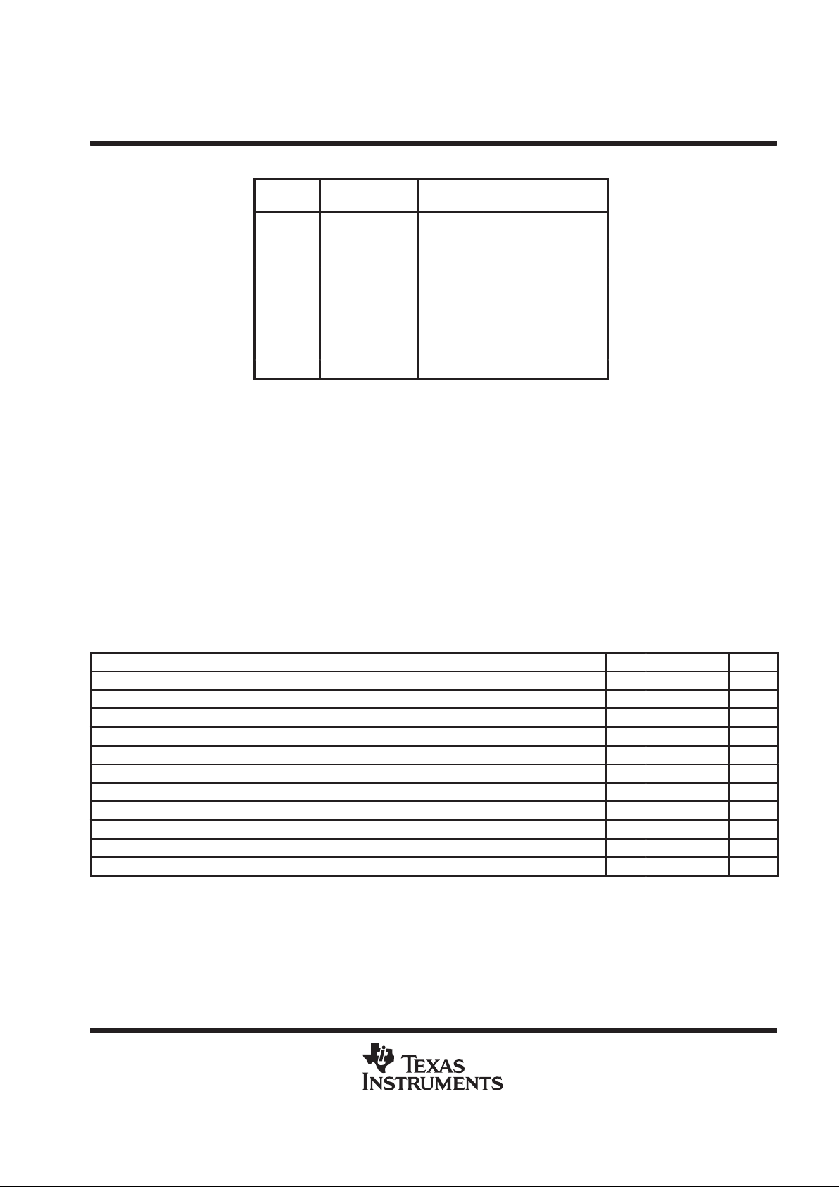
FUNCTION TABLE
STEP
ANALOG INPUT
VOLTAGE
DIGITAL OUTPUT CODE
0 3.992 V L L L L L L
1 4.008 V L LL LLH
| | |
31 4.488 V L HH HHH
32 4.508 V H LL LLL
33 4.520 V H LL LLH
| | |
62 4.984 V H HH HHL
63 5.000 V H H H H H H
†
These values are based on the assumption that V
refB
and V
refT
have been
adjusted so that the voltage at the transition from digital 0 to 1 (VZT) is
4.000 V and the transition to full scale (VFT) is 4.992 V . 1 LSB = 16 mV.
absolute maximum ratings over operating free-air temperature range (unless otherwise noted)
Supply voltage range, ANLG VCC (see Note 1) –0.5 V to 7 V. . . . . . . . . . . . . . . . . . . . . . . . . . . . . . . . . . . . . . . .
Supply voltage range, DGTL V
CC
–0.5 V to 7 V. . . . . . . . . . . . . . . . . . . . . . . . . . . . . . . . . . . . . . . . . . . . . . . . . . . .
Input voltage range at digital input, V
I
–0.5 V to 7 V. . . . . . . . . . . . . . . . . . . . . . . . . . . . . . . . . . . . . . . . . . . . . . . . .
Input voltage range at analog input, V
I
–0.5 V to ANLG VCC +0.5 V. . . . . . . . . . . . . . . . . . . . . . . . . . . . . . . . . .
Analog reference voltage range, V
ref
–0.5 V to ANLG V
CC
+0.5 V. . . . . . . . . . . . . . . . . . . . . . . . . . . . . . . . . . .
Storage temperature range –55°C to 150°C. . . . . . . . . . . . . . . . . . . . . . . . . . . . . . . . . . . . . . . . . . . . . . . . . . . . . . . .
Operating free-air temperature range 0°C to 70°C. . . . . . . . . . . . . . . . . . . . . . . . . . . . . . . . . . . . . . . . . . . . . . . . . .
Lead temperature 1,6 mm (1/16 inch) from case for 10 seconds 260°C. . . . . . . . . . . . . . . . . . . . . . . . . . . . . . .
NOTE 1: All voltage values are with respect to the network ground terminal.
recommended operating conditions
MIN NOM MAX UNIT
Supply voltage, ANLG V
CC
4.75 5 5.25 V
Supply voltage, DGTL V
CC
4.75 5 5.25 V
High-level input voltage, V
IH
2 V
Low-level input voltage, V
IL
0.8 V
Input voltage at analog input, VI (see Note 2) 4 5 V
Analog reference voltage (top side), V
refT
(see Note 2) 4 5 5.1 V
Analog reference voltage (bottom side), V
refB
(see Note 2) 3 4 4.1 V
High-level output current, I
OH
–400 µA
Low-level output current, I
OL
4 mA
Clock pulse duration, high-level or low-level, t
w
25 ns
Operating free-air temperature, T
A
0 70 °C
NOTE 2: V
refB
< VI < V
refT
, V
refT
– V
refB
= 1 V ±0.1 V.

TL5501
6-BIT ANALOG-TO-DIGITAL CONVERTER
SLAS026 – OCTOBER 1989 – REVISED APRIL 1990
4
POST OFFICE BOX 655303 • DALLAS, TEXAS 75265
electrical characteristics over operating supply voltage range, TA = 25°C (unless otherwise noted)
PARAMETER TEST CONDITIONS MIN TYP MAX UNIT
p
VI = 5 V 75
IIAnalog input current
VI = 4 V 73
µ
A
I
IH
Digital high-level input current VI = 2.7 V 0 20 µA
I
IL
Digital low-level input current VI = 0.4 V – 400 –40 µA
I
I
Digital input current VI = 7 V 100 µA
I
refB
Reference current V
IrefB
= 4 V –4 –7.2 mA
I
refT
Reference current V
IrefB
= 5 V 4 7.2 mA
V
OH
High-level output voltage IOH = –400 µA 2.7 V
V
OL
Low-level output voltage IOL = 1.6 mA 0.4 V
r
i
Analog input resistance 100 kΩ
1CiAnalog input capacitance 35 65 pF
I
CC
Supply current 40 60 mA
operating characteristics over operating supply voltage range, TA = 25°C (unless otherwise noted)
PARAMETER TEST CONDITIONS MIN TYP†MAX UNIT
E
L
Linearity error ±0.8 %FSR
f
max
Maximum converstion rate 20 30 MHz
t
d
Digital output delay time See Figure 3 15 30 ns
†
All typical values are at VCC = 5 V, Vref = 4 V, TA = 25°C.
timing diagram
Data
N + 1
Data
N
N – 1
Data
t
d
INPUT
D1–D6
ANLG
CLK
1.4 V
t
wL
t
wH
N + 2N + 1N
SampleSampleSample

TL5501
6-BIT ANALOG-TO-DIGITAL CONVERTER
SLAS026 – OCTOBER 1989 – REVISED APRIL 1990
5
POST OFFICE BOX 655303 • DALLAS, TEXAS 75265
TYPICAL CHARACTERISTICS
4.984
5.000
4.992 V
4.968
4.520
4.504
4.488
4.024
4.008
3.992
See Note A
1/2 LSB
VFT = V
FS
V
FS
V
ZT
VZS + 1/2 LSB
V
ZS
Step
Digital Output CodeS
63
62
61
33
32
31
2
1
0
VI — Analog Input Voltage — V
111111
111110
S111101
100001
100000
011111
000000
000001
000010
IDEAL CONVERSION CHARACTERISTICS
NOTE A: This curve is based on the assumption that V
refB
and V
refT
have been
adjusted so that the voltage at the transition from digital 0 to 1 (VZT) is
4.000 V and the transition to full scale (VFT) is 4.992 V . 1 LSB = 16 mV .
Figure 1
Step
Digital Output Code
000010
000001
000000
011111
100000
100001
111101
111110
111111
VI — Analog Input Voltage — V
0
1
2
31
32
33
61
62
63
E
L61
E
L33
E
L32
E
L31
E
L2
E
L1
END-POINT LINEARITY ERROR
Figure 2

TL5501
6-BIT ANALOG-TO-DIGITAL CONVERTER
SLAS026 – OCTOBER 1989 – REVISED APRIL 1990
6
POST OFFICE BOX 655303 • DALLAS, TEXAS 75265
PARAMETER MEASUREMENT INFORMATION
Output
Digital
To
V
CC
Point
Measurement
RL = 2 kΩ
CL = 15 pF
Figure 3. Load Circuit

IMPORTANT NOTICE
T exas Instruments and its subsidiaries (TI) reserve the right to make changes to their products or to discontinue
any product or service without notice, and advise customers to obtain the latest version of relevant information
to verify, before placing orders, that information being relied on is current and complete. All products are sold
subject to the terms and conditions of sale supplied at the time of order acknowledgement, including those
pertaining to warranty, patent infringement, and limitation of liability.
TI warrants performance of its semiconductor products to the specifications applicable at the time of sale in
accordance with TI’s standard warranty. Testing and other quality control techniques are utilized to the extent
TI deems necessary to support this warranty. Specific testing of all parameters of each device is not necessarily
performed, except those mandated by government requirements.
CERT AIN APPLICATIONS USING SEMICONDUCTOR PRODUCTS MAY INVOLVE POTENTIAL RISKS OF
DEATH, PERSONAL INJURY, OR SEVERE PROPERTY OR ENVIRONMENTAL DAMAGE (“CRITICAL
APPLICATIONS”). TI SEMICONDUCTOR PRODUCTS ARE NOT DESIGNED, AUTHORIZED, OR
WARRANTED TO BE SUITABLE FOR USE IN LIFE-SUPPORT DEVICES OR SYSTEMS OR OTHER
CRITICAL APPLICATIONS. INCLUSION OF TI PRODUCTS IN SUCH APPLICA TIONS IS UNDERST OOD TO
BE FULLY AT THE CUSTOMER’S RISK.
In order to minimize risks associated with the customer’s applications, adequate design and operating
safeguards must be provided by the customer to minimize inherent or procedural hazards.
TI assumes no liability for applications assistance or customer product design. TI does not warrant or represent
that any license, either express or implied, is granted under any patent right, copyright, mask work right, or other
intellectual property right of TI covering or relating to any combination, machine, or process in which such
semiconductor products or services might be or are used. TI’s publication of information regarding any third
party’s products or services does not constitute TI’s approval, warranty or endorsement thereof.
Copyright 1998, Texas Instruments Incorporated
 Loading...