

TL3695
DIFFERENTIAL BUS TRANSCEIVER
SLLS044D – NOVEMBER 1988 – REVISED DECEMBER 1999
1
POST OFFICE BOX 655303 • DALLAS, TEXAS 75265
D
Bidirectional Transceiver
D
Meets or Exceeds the Requirements of
TIA/EIA-422-B, TIA/EIA-485-A, and ITU
Recommendation V.11
D
High-Speed Advanced Low-Power Schottky
Circuitry
D
Low Skew ...6 ns Max
D
Designed for Multipoint Transmission on
Long Bus Lines in Noisy Environments
D
Low Supply-Current Requirements . . .
30 mA Max
D
Wide Positive and Negative Input/Output
Bus-Voltage Ranges
D
Driver Output Capacity . . . ±60 mA
D
Thermal-Shutdown Protection
D
Driver Positive and Negative Current
Limiting
D
Receiver Input Impedances . . . 12 kΩ Min
D
Receiver Input Sensitivity . . . ±200 mV Max
D
Receiver Input Hysteresis . . . 120 mV T yp
D
Fail Safe . . . High Receiver Output With
Inputs Open
D
Operates From a Single 5-V Supply
D
Glitch-Free Power-Up and Power-Down
Protection
D
Interchangeable With National DS3695 and
DS3695A
description
The TL3695 differential bus transceiver is designed for bidirectional data communication on multipoint
bus-transmission lines. It is designed for balanced transmission lines and meets TIA/EIA-422-B,
TIA/EIA-485-A, and ITU Recommendation V.11.
The TL3695 combines a 3-state differential line driver and a differential input line receiver , both of which operate
from a single 5-V power supply . The driver and receiver have active-high and active-low enables, respectively ,
which can be externally connected together to function as a directional control. The driver differential outputs
and the receiver differential inputs are connected internally to form a differential input/output (I/O) bus port that
is designed to offer minimum loading to the bus when the driver is disabled or V
CC
= 0. This port features wide
positive and negative common-mode voltage ranges, making the device suitable for party line applications.
The TL3695 is characterized for operation from 0°C to 70°C.
Copyright 1999, Texas Instruments Incorporated
PRODUCTION DATA information is current as of publication date.
Products conform to specifications per the terms of Texas Instruments
standard warranty. Production processing does not necessarily include
testing of all parameters.
Please be aware that an important notice concerning availability, standard warranty, and use in critical applications of
Texas Instruments semiconductor products and disclaimers thereto appears at the end of this data sheet.
1
2
3
4
8
7
6
5
R
RE
DE
D
V
CC
B
A
GND
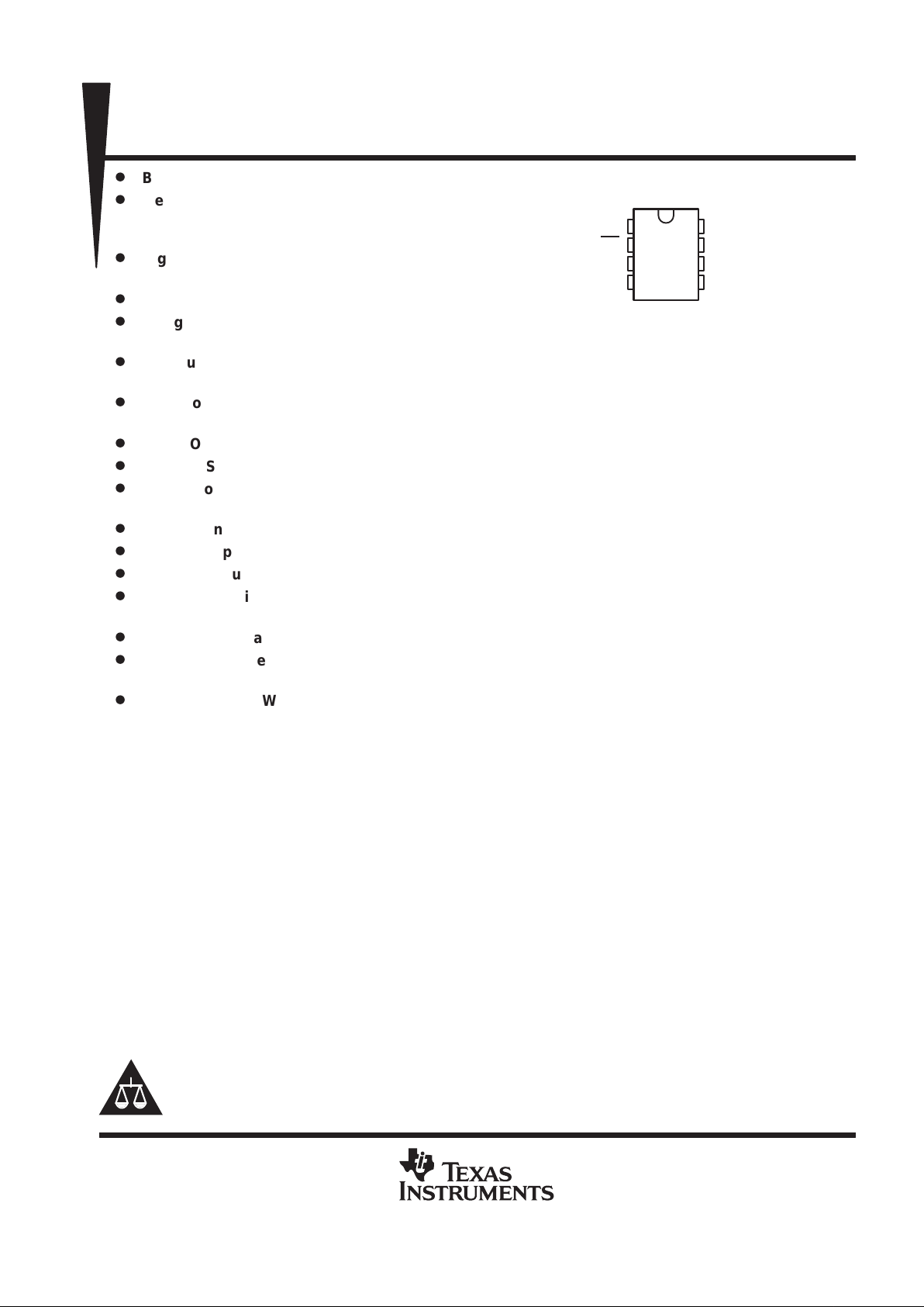
D OR P PACKAGE
(TOP VIEW)
TL3695
DIFFERENTIAL BUS TRANSCEIVER
SLLS044D – NOVEMBER 1988 – REVISED DECEMBER 1999
2
POST OFFICE BOX 655303 • DALLAS, TEXAS 75265
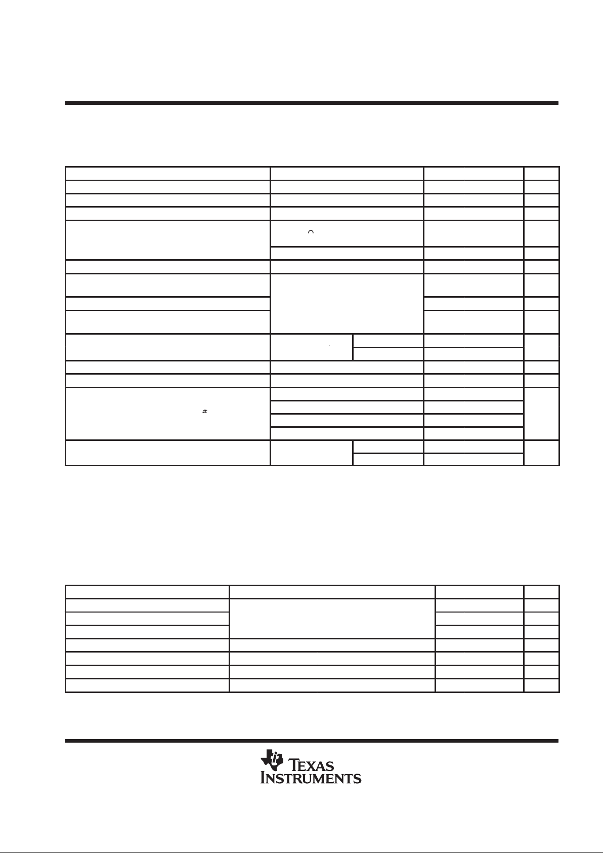
AVAILABLE OPTIONS
PACKAGED DEVICES
T
A
SMALL OUTLINE
(D)
PLASTIC DIP
(P)
0°C to 70°C TL3695D TL3695P
The D package is available taped and reeled. Add the suffix R
to device type (e.g., TL3695DR).
Function Tables
DRIVER
INPUT
ENABLE
OUTPUTS
D DE
A B
H H H L
L H L H
X L Z Z
H = high level, L = low level, ? = indeterminate,
X = irrelevant, Z = high impedance (off)
RECEIVER
DIFFERENTIAL INPUTS
ENABLE OUTPUT
A – B RE R
VID ≥ 0.2 V L H
–0.2 V < VID < 0.2 V L ?
VID ≤ –0.2 V L L
X H Z
Inputs open L H
H = high level, L = low level, ? = indeterminate, X = irrelevant,
Z = high impedance (off)
logic symbol
†
†
This symbol is in accordance with ANSI/IEEE Std 91-1984 and
IEC Publication 617-12.
EN1
3
DE
EN2
2
A
6
1
B
7
1
R
1
2
4
D
RE
logic diagram (positive logic)
2
B
7
A
6
1
R
3
DE
4
D
Bus
RE
TL3695
DIFFERENTIAL BUS TRANSCEIVER
SLLS044D – NOVEMBER 1988 – REVISED DECEMBER 1999
3
POST OFFICE BOX 655303 • DALLAS, TEXAS 75265
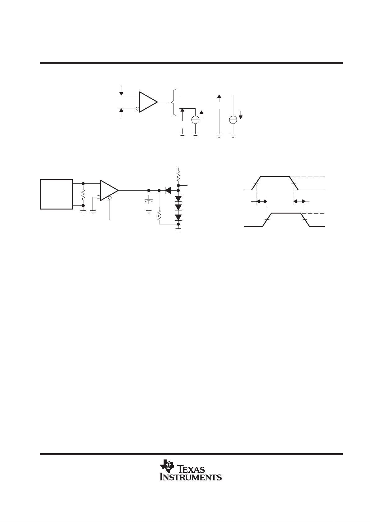
schematic of inputs and outputs
EQUIVALENT OF EACH INPUT
V
CC
R
(eq)
Input
Driver Input: R
(eq)
= 3 kΩ NOM
Enable Inputs: R
(eq)
= 8 kΩ NOM
R
(eq)
= equivalent resistor
TYPICAL OF A AND B I/O PORTS
V
CC
180 kΩ
NOM
Connected
on A Port
180 kΩ
NOM
Connected
on B Port
A or B
18 kΩ
NOM
3 kΩ
NOM
1.1 kΩ
NOM
TYPICAL OF RECEIVER OUTPUT
V
CC
85 Ω
NOM
Output
absolute maximum ratings over operating free-air temperature range (unless otherwise noted)
†
Supply voltage, VCC (see Note 1) 7 V. . . . . . . . . . . . . . . . . . . . . . . . . . . . . . . . . . . . . . . . . . . . . . . . . . . . . . . . . . . . .
Voltage range at any bus terminal –10 V to 15 V. . . . . . . . . . . . . . . . . . . . . . . . . . . . . . . . . . . . . . . . . . . . . . . . . . . .
Enable input voltage, VI 5.5 V. . . . . . . . . . . . . . . . . . . . . . . . . . . . . . . . . . . . . . . . . . . . . . . . . . . . . . . . . . . . . . . . . . . .
Operating free-air temperature range, TA 0°C to 70°C. . . . . . . . . . . . . . . . . . . . . . . . . . . . . . . . . . . . . . . . . . . . . .
Package thermal impedance, θJA (see Note 2): D package 97°C/W. . . . . . . . . . . . . . . . . . . . . . . . . . . . . . . . . . .
PW package 85°C/W. . . . . . . . . . . . . . . . . . . . . . . . . . . . . . . . .
Lead temperature 1,6 mm (1/16 inch) from case for 10 seconds 260°C. . . . . . . . . . . . . . . . . . . . . . . . . . . . . . .
Storage temperature range, T
stg
–65°C to 150°C. . . . . . . . . . . . . . . . . . . . . . . . . . . . . . . . . . . . . . . . . . . . . . . . . . .
†
Stresses beyond those listed under “absolute maximum ratings” may cause permanent damage to the device. These are stress ratings only, and
functional operation of the device at these or any other conditions beyond those indicated under “recommended operating conditions” is not
implied. Exposure to absolute-maximum-rated conditions for extended periods may affect device reliability.
NOTES: 1. All voltage values, except differential I/O bus voltage, are with respect to network ground terminal.
2. The package thermal impedance is calculated in accordance with JESD 51.
TL3695
DIFFERENTIAL BUS TRANSCEIVER
SLLS044D – NOVEMBER 1988 – REVISED DECEMBER 1999
4
POST OFFICE BOX 655303 • DALLAS, TEXAS 75265
recommended operating conditions
MIN NOM MAX UNIT
Supply voltage, V
CC
4.75 5 5.25 V
p
12
Voltage at any bus terminal (separately or common mode), V
I
or V
IC
–7
V
High-level Input voltage, V
IH
D, DE, and RE 2 V
Low-level Input voltage, V
IL
D, DE, and RE 0.8 V
Differential input voltage, VID (see Note 3) ±12 V
p
Driver –60 mA
High-level output current, I
OH
Receiver – 400 µA
p
Driver 60
Low-level output current, I
OL
Receiver 8
mA
Operating free-air temperature, T
A
0 70 °C
NOTE 3: Differential input/output bus voltage is measured at the noninverting terminal A with respect to the inverting terminal B.
TL3695
DIFFERENTIAL BUS TRANSCEIVER
SLLS044D – NOVEMBER 1988 – REVISED DECEMBER 1999
5
POST OFFICE BOX 655303 • DALLAS, TEXAS 75265
DRIVER SECTION
electrical characteristics over recommended ranges of supply voltage and operating free-air
temperature (unless otherwise noted)
PARAMETER TEST CONDITIONS
†
MIN TYP‡MAX UNIT
V
IK
Input clamp voltage II = –18 mA –1.5 V
V
O
Output voltage IO = 0 0 6 V
|V
OD1
| Differential output voltage IO = 0 1.5 5 V
1/2V
|V
OD2
| Differential output voltage
R
L
=
100 Ω
,
See Figure 1
OD1
or 2
§
V
RL = 54 Ω, See Figure 1 1.5 2.5 5 V
V
OD3
Differential output voltage V
test
= –7 V to 12 V, See Figure 2 1.5 5 V
∆ |VOD|
Change in magnitude of differential output
voltage
¶
±0.2 V
V
OC
Common-mode output voltage
RL = 54 Ω, See Figure 1
3 V
∆ |VOC|
Change in magnitude of common-mode
output voltage
¶
±0.2 V
p
Output disabled,
VO = 12 V 1
IOOutput current
,
See Note 4
VO = –7 V –0.8
mA
I
IH
High-level input current VI = 2.4 V 20 µA
I
IL
Low-level input current VI = 0.4 V –200 µA
VO = –6 V –250
p
VO = 0 –150
IOSShort-circuit output current
#
VO = V
CC
250
mA
VO = 8 V 250
pp
Outputs enabled 23 50
ICCSupply current
No load
Outputs disabled 19 35
mA
†
The power-off measurement in TIA/EIA-422-B applies to disabled outputs only and is not applied to combined inputs and outputs.
‡
All typical values are at VCC = 5 V and TA = 25°C.
§
The minimum V
OD2
with a 100-Ω load is either 1/2 V
OD1
or 2 V, whichever is greater.
¶
∆ |VOD| and ∆ |VOC| are the changes in magnitude of VOD and VOC, respectively, that occur when the input is changed from a high level to a low
level.
#
Duration of the short circuit should not exceed one second for this test.
NOTE 4: This applies for power on and power off. Refer to TIA/EIA-485-A for exact conditions. The TIA/EIA-422-B limit does not apply for a
combined driver and receiver terminal.
switching characteristics over recommended ranges of supply voltage and operating free-air
temperature
PARAMETER TEST CONDITIONS MIN TYP‡MAX UNIT
t
d(OD)
Differential-output delay time 8 22 ns
Skew (|t
d(ODH)
– t
d(ODL)
|)
CL1 = CL2 = 100 pF, RL = 60 Ω, See Figure 3
1 8 ns
t
t(OD)
Differential output transition time 8 18 ns
t
PZH
Output enable time to high level CL = 100 pF, RL = 500 Ω, See Figure 4 50 ns
t
PZL
Output enable time to low level CL = 100 pF, RL = 500 Ω, See Figure 5 50 ns
t
PHZ
Output disable time from high level CL = 15 pF, RL = 500 Ω, See Figure 4 8 30 ns
t
PLZ
Output disable time from low level CL = 15 pF, RL = 500 Ω, See Figure 5 8 30 ns
‡
All typical values are at VCC = 5 V and TA = 25°C.

TL3695
DIFFERENTIAL BUS TRANSCEIVER
SLLS044D – NOVEMBER 1988 – REVISED DECEMBER 1999
6
POST OFFICE BOX 655303 • DALLAS, TEXAS 75265
SYMBOL EQUIVALENTS
DATA-SHEET PARAMETER
TIA/EIA-422-B TIA/EIA-485-A
V
O
Voa, V
ob
Voa, V
ob
|V
OD1
| V
o
V
o
|V
OD2
| Vt (RL = 100 Ω) Vt (RL = 54 Ω)
|V
OD3
|
Vt (test termination
measurement 2)
V
test
V
tst
∆ |VOD| | |Vt| – |V
t
| |
| |Vt| – |V
t
| |
V
OC
|Vos| |Vos|
∆ |VOC| | Vos – V
os
|
| Vos – V
os
|
I
OS
| Isa |, | Isb |
I
O
| Ixa |, | Ixb | Iia, I
ib
RECEIVER SECTION
electrical characteristics over recommended ranges of common-mode input voltage, supply
voltage, and operating free-air temperature range (unless otherwise noted)
PARAMETER TEST CONDITIONS MIN TYP†MAX UNIT
V
IT+
Positive-going input threshold voltage VO = 2.7 V, IO = –0.4 mA 0.2 V
V
IT–
Negative-going input threshold voltage VO = 0.5 V, IO = 8 mA –0.2
‡
V
V
hys
Hysteresis voltage (V
IT+–VIT–
) VOC = 0 70 mV
V
IK
Enable-input clamp voltage II = –18 mA –1.5 V
p
V
= 200 mV or inputs open,
VOHHigh-level output voltage
ID
,
IOH = –400 µA, See Figure 6
2.4
V
p
V
= –200 mV,
IOL = 16 mA 0.5
VOLLow-level output voltage
ID
,
See Figure 6
IOL = 8 mA 0.45
V
I
OZ
High-impedance-state output current VO = 0.4 V to 2.4 V ±20 µA
p
Other input = 0,
VI = 12 V 1
IILine input current
,
See Note 5
VI = –7 V –0.8
mA
I
IH
High-level enable-input current VIH = 2.7 V 20 µA
I
IL
Low-level enable-input current VIL = 0.4 V –100 µA
r
I
Input resistance 12 kΩ
I
OS
Short-circuit output current
§
VO = 0 –15 –85 mA
pp
Outputs enabled 23 50
ICCSupply current
No load
Outputs disabled 19 35
mA
†
All typical values are at VCC = 5 V and TA = 25°C.
‡
The algebraic convention, in which the less positive (more negative) limit is designated minimum, is used in this data sheet for common-mode
input voltage and threshold voltage levels only.
§
Duration of the short circuit should not exceed one second for this test.
NOTE 5: This applies for power on and power off. Refer to TIA/EIA-485-A for exact conditions.

TL3695
DIFFERENTIAL BUS TRANSCEIVER
SLLS044D – NOVEMBER 1988 – REVISED DECEMBER 1999
7
POST OFFICE BOX 655303 • DALLAS, TEXAS 75265
switching characteristics over recommended ranges of supply voltage and operating free-air
temperature range, C
L
= 15 pF
PARAMETER TEST CONDITIONS MIN TYP†MAX UNIT
t
PLH
Propagation delay time, low- to high-level output
V
= –1.5 V to 1.5 V,
14 37 ns
t
PHL
Propagation delay time, high- to low-level output
ID
,
See Figure 7
14 37 ns
t
PZH
Output enable time to high level
7 20 ns
t
PZL
Output enable time to low level
See Figure 8
7 20 ns
t
PHZ
Output disable time from high level
7 16 ns
t
PLZ
Output disable time from low level
See Figure 8
8 16 ns
†
All typical values are at VCC = 5 V and TA = 25°C.
PARAMETER MEASUREMENT INFORMATION
V
OD2
V
OC
R
L
2
R
L
2
Figure 1. Driver VOD and V
OC
V
OD3
375 Ω
375 Ω
60 Ω
V
test
Figure 2. Driver V
OD3
50 Ω
Generator
(see Note B)
3 V
CL1 = 100 pF
(see Note A)
CL2 = 100 pF
(see Note A)
RL = 60 Ω
Output
Output
Input
t
d(ODH)
t
d(ODL)
t
t(OD)
t
t(OD)
3 V
0 V
≈2.5 V
≈ –2.5 V
50%
50%
90%
10%
1.5 V
1.5 V
TEST CIRCUIT
VOLTAGE WAVEFORMS
NOTES: A. CL includes probe and jig capacitance.
B. The input pulse is supplied by a generator having the following characteristics: PRR ≤ 1 MHz, 50% duty cycle, tr ≤ 6 ns, tf ≤ 6 ns,
ZO = 50 Ω.
Figure 3. Driver Differential-Output Test Circuit and Voltage Waveforms

TL3695
DIFFERENTIAL BUS TRANSCEIVER
SLLS044D – NOVEMBER 1988 – REVISED DECEMBER 1999
8
POST OFFICE BOX 655303 • DALLAS, TEXAS 75265
PARAMETER MEASUREMENT INFORMATION
t
PHZ
Generator
(see Note B)
50 Ω
0 V to 3 V
3 V
0 V
Output
S1
C
L
(see Note A)
RL = 500 Ω
1.5 V 1.5 V
Input
Output
t
PZH
2.3 V
0.5 V
V
OH
V
off
≈0 V
TEST CIRCUIT
VOLTAGE WAVEFORMS
NOTES: A. CL includes probe and jig capacitance.
B. The input pulse is supplied by a generator having the following characteristics: PRR ≤ 1 MHz, 50% duty cycle, tr ≤ 10 ns,
tf ≤ 10 ns, ZO = 50 Ω.
Figure 4. Driver Test Circuit and Voltage Waveforms
Generator
(see Note B)
3 V or 0 V
50 Ω
S1
RL = 500 Ω
Output
Output
5 V
CL
(see Note A)
Input
3 V
0 V
5 V
0.5 V
V
OL
1.5 V
2.3 V
1.5 V
t
PZL
t
PLZ
TEST CIRCUIT
VOLTAGE WAVEFORMS
NOTES: A. CL includes probe and jig capacitance.
B. The input pulse is supplied by a generator having the following characteristics: PRR ≤ 1 MHz, 50% duty cycle, tr ≤ 10 ns,
tf ≤ 10 ns, ZO = 50 Ω..
Figure 5. Driver Test Circuit and Voltage Waveforms
TL3695
DIFFERENTIAL BUS TRANSCEIVER
SLLS044D – NOVEMBER 1988 – REVISED DECEMBER 1999
9
POST OFFICE BOX 655303 • DALLAS, TEXAS 75265
PARAMETER MEASUREMENT INFORMATION
+I
OL
V
ID
V
OL
V
OH
–I
OH
Figure 6. Receiver VOH and V
OL
Generator
(see Note B)
0 V
5 V
51 Ω
CL = 15 pF
(see Note A)
1 kΩ
1 kΩ
1N916
or
Equivalent
Input
Output
0 V 0 V
2.5 V
–2.5 V
1.5 V
1.5 V
V
OH
V
OL
t
PLH
t
PHL
TEST CIRCUIT VOLTAGE WAVEFORMS
NOTES: A. CL includes probe and jig capacitance.
B. The input pulse is supplied by a generator having the following characteristics: PRR ≤ 1 MHz, 50% duty cycle, tr ≤ 10 ns,
tf ≤ 10 ns, ZO = 50 Ω.
Output
Figure 7. Receiver Test Circuit and Voltage Waveforms

TL3695
DIFFERENTIAL BUS TRANSCEIVER
SLLS044D – NOVEMBER 1988 – REVISED DECEMBER 1999
10
POST OFFICE BOX 655303 • DALLAS, TEXAS 75265
PARAMETER MEASUREMENT INFORMATION
1.5 V
–1.5 V
1.5 V
1.5 V
1.5 V
0.5 V
50 Ω
Generator
(see Note B)
S1
S3
1 kΩ
CL = 15 pF
(see Note A)
1N916 or Equivalent
3 V
0 V
0 V
Input
Input
Output
Output
t
PZH
TEST CIRCUIT
V
OH
S1 to 1.5 V
S2 Open
S3 Closed
Input
Output
Input
Output
t
PZL
3 V
1.5 V
0 V
1.5 V
V
OL
≈4.5 V
≈1.3 V
S1 to –1.5 V
S2 Closed
S3 Open
S1 to –1.5 V
S2 Closed
S3 Open
3 V
0 V
S1 to 1.5 V
S2 Open
S3 Closed
t
PHZ
V
OH
≈1.3 V
3 V
0 V
1.5 V
t
PLZ
0.5 V
V
OL
VOLTAGE WAVEFORMS
NOTES: A. CL includes probe and jig capacitance.
B. The input pulse is supplied by a generator having the following characteristics: PRR ≤ 1 MHz, 50% duty cycle, tr ≤ 10 ns,
tf ≤ 10 ns, ZO = 50 Ω.
2 kΩ
5 V
S2
Output
Figure 8. Receiver Test Circuit and Voltage Waveforms

TL3695
DIFFERENTIAL BUS TRANSCEIVER
SLLS044D – NOVEMBER 1988 – REVISED DECEMBER 1999
11
POST OFFICE BOX 655303 • DALLAS, TEXAS 75265
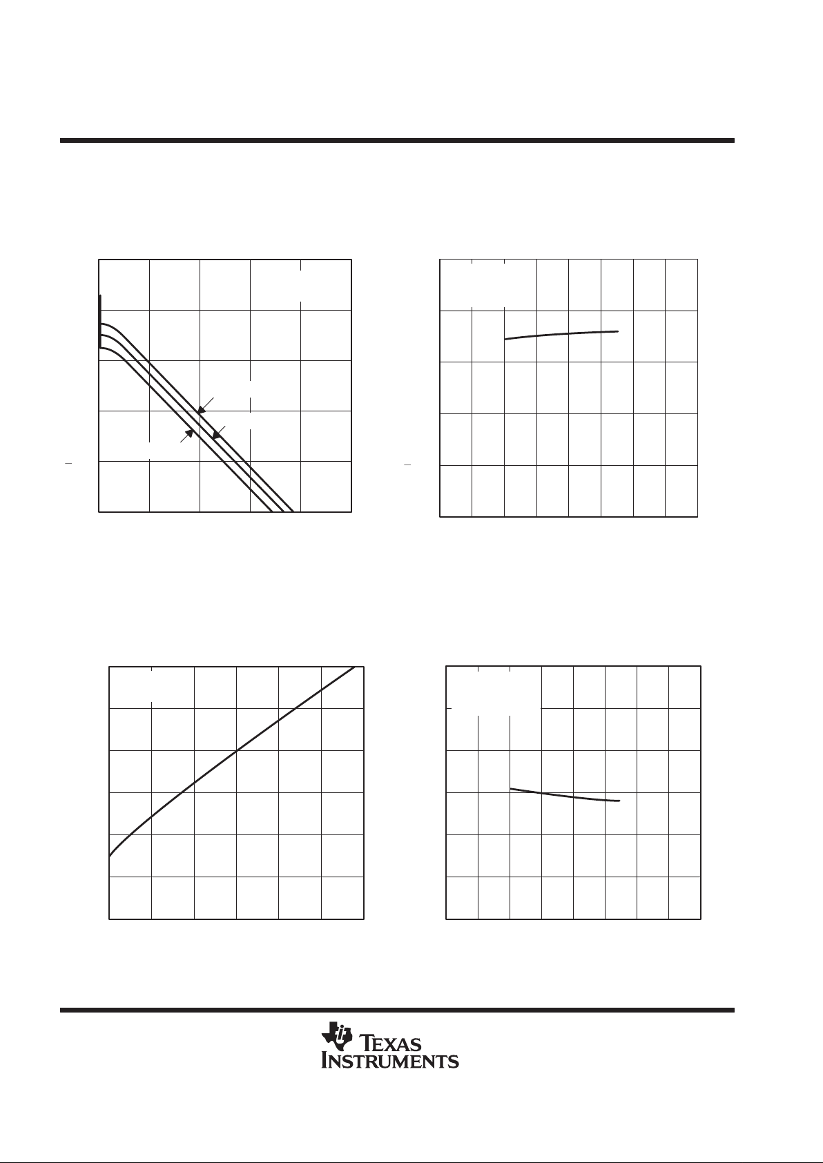
TYPICAL CHARACTERISTICS
†
Figure 9
–20
1.5
1
0.5
0
0
2
2.5
3
3.5
4
4.5
5
DRIVER
HIGH-LEVEL OUTPUT VOLTAGE
vs
HIGH-LEVEL OUTPUT CURRENT
IOH – High-Level Output Current – mA
V0H – High-Level Output Voltage – V
V
OH
VCC = 5 V
TA = 25°C
–40 –60 –80 –100 – 120
VOL – Low-Level Output V oltage – V
V
OL
1.5
1
0.5
0
02040 60
2
2.5
3
80 100 120
3.5
4
4.5
5
DRIVER
LOW-LEVEL OUTPUT VOLTAGE
vs
LOW-LEVEL OUTPUT CURRENT
IOL – Low-Level Output Current – mA
VCC = 5 V
TA = 25°C
Figure 10
2
1.5
0.5
0
0102030405060
3
4
70
1
3.5
2.5
80 90 100
IO – Output Current – mA
DRIVER
DIFFERENTIAL OUTPUT VOLTAGE
vs
OUTPUT CURRENT
VOD – Differential Output Voltage – V
V
OD
VCC = 5 V
TA = 25°C
Figure 11
†
Operation of the device at these or any other conditions beyond those indicated under ‘‘recommended operating conditions” is not implied.
TL3695
DIFFERENTIAL BUS TRANSCEIVER
SLLS044D – NOVEMBER 1988 – REVISED DECEMBER 1999
12
POST OFFICE BOX 655303 • DALLAS, TEXAS 75265
TYPICAL CHARACTERISTICS
†
Figure 12
–10
2
1
0
0
3
4
5
RECEIVER
HIGH-LEVEL OUTPUT VOLTAGE
vs
HIGH-LEVEL OUTPUT CURRENT
IOH – High-Level Output Current – mA
V0H – High-Level Output Voltage – V
V
OH
VCC = 5.25 V
VCC = 4.75 V
–20 –30 –40 –50
VID = 0.2 V
TA = 25°C
VCC = 5 V
2
0
0 204060805100 120
4
3
1
RECEIVER
HIGH-LEVEL OUTPUT VOLTAGE
vs
FREE-AIR TEMPERATURE
V0H – High-Level Output Voltage – V
V
OH
TA – Free-Air Temperature – °C
–40 –20
VCC = 5 V
VID = 200 mV
IOH = –440 µA
Figure 13
Figure 14
0.3
0.2
0.1
0
0510
0.4
0.5
0.6
15 20 25
30
RECEIVER
LOW-LEVEL OUTPUT VOLTAGE
vs
LOW-LEVEL OUTPUT CURRENT
IOL – Low-Level Output Current – mA
VOL – Low-Level Output V oltage – V
V
OL
VCC = 5 V
TA = 25°C
Figure 15
–40
0.3
0.2
0.1
0
0204060
0.4
0.5
0.6
80 100 120
RECEIVER
LOW-LEVEL OUTPUT VOLTAGE
vs
FREE-AIR TEMPERATURE
VOL – Low-Level Output V oltage – V
V
OL
TA – Free-Air Temperature – °C
VCC = 5 V
VID = –200 mV
IOL = 8 mA
–20
†
Operation of the device at these or any other conditions beyond those indicated under ‘‘recommended operating conditions” is not implied.

TL3695
DIFFERENTIAL BUS TRANSCEIVER
SLLS044D – NOVEMBER 1988 – REVISED DECEMBER 1999
13
POST OFFICE BOX 655303 • DALLAS, TEXAS 75265
TYPICAL CHARACTERISTICS
†
Figure 16
1
0
0 0.5 1 1.5
2
3
2 2.5 3
4
5
RECEIVER
OUTPUT VOLTAGE
vs
ENABLE VOLTAGE
V) – Output Voltage – V
V
O
VI – Enable Voltage – V
VCC = 4.75 V
VCC = 5 V
VID = 0.2 V
Load = 8 kΩ to GND
TA = 25°C
VCC = 5.25 V
Figure 17
3
2
1
0
0 0.5 1
4
5
6
1.5 2 2.5 3
RECEIVER
OUTPUT VOLTAGE
vs
ENABLE VOLTAGE
V) – Output Voltage – V
V
O
VI – Enable Voltage – V
VCC = 5.25 V
VCC = 4.75 V
VCC = 5 V
VID = –0.2 V
Load = 1 kΩ to V
CC
TA = 25°C
†
Operation of the device at these or any other conditions beyond those indicated under ‘‘recommended operating conditions” is not implied.
APPLICATION INFORMATION
TL3695 TL3695
Up to 32
Transceivers
R
T
R
T
NOTE A: The line should be terminated at both ends in its characteristic impedance (RT = ZO). Stub lengths off the main line should be kept
as short as possible.
Figure 18. Typical Application Circuit

IMPORTANT NOTICE
T exas Instruments and its subsidiaries (TI) reserve the right to make changes to their products or to discontinue
any product or service without notice, and advise customers to obtain the latest version of relevant information
to verify, before placing orders, that information being relied on is current and complete. All products are sold
subject to the terms and conditions of sale supplied at the time of order acknowledgement, including those
pertaining to warranty, patent infringement, and limitation of liability.
TI warrants performance of its semiconductor products to the specifications applicable at the time of sale in
accordance with TI’s standard warranty. Testing and other quality control techniques are utilized to the extent
TI deems necessary to support this warranty. Specific testing of all parameters of each device is not necessarily
performed, except those mandated by government requirements.
CERT AIN APPLICATIONS USING SEMICONDUCTOR PRODUCTS MAY INVOLVE POTENTIAL RISKS OF
DEATH, PERSONAL INJURY, OR SEVERE PROPERTY OR ENVIRONMENTAL DAMAGE (“CRITICAL
APPLICATIONS”). TI SEMICONDUCTOR PRODUCTS ARE NOT DESIGNED, AUTHORIZED, OR
WARRANTED TO BE SUITABLE FOR USE IN LIFE-SUPPORT DEVICES OR SYSTEMS OR OTHER
CRITICAL APPLICATIONS. INCLUSION OF TI PRODUCTS IN SUCH APPLICA TIONS IS UNDERSTOOD T O
BE FULLY AT THE CUSTOMER’S RISK.
In order to minimize risks associated with the customer’s applications, adequate design and operating
safeguards must be provided by the customer to minimize inherent or procedural hazards.
TI assumes no liability for applications assistance or customer product design. TI does not warrant or represent
that any license, either express or implied, is granted under any patent right, copyright, mask work right, or other
intellectual property right of TI covering or relating to any combination, machine, or process in which such
semiconductor products or services might be or are used. TI’s publication of information regarding any third
party’s products or services does not constitute TI’s approval, warranty or endorsement thereof.
Copyright 2000, Texas Instruments Incorporated
 Loading...