

TL3016, TL3016Y
ULTRA-FAST LOW-POWER
PRECISION COMPARATORS
SLCS130D – MARCH 1997 – REVISED MARCH 2000
1
POST OFFICE BOX 655303 • DALLAS, TEXAS 75265
D
Ultrafast Operation . . . 7.6 ns (Typ)
D
Low Positive Supply Current
10.6 mA (Typ)
D
Operates From a Single 5-V Supply or From
a Split ±5-V Supply
D
Complementary Outputs
D
Low Offset Voltage
D
No Minimum Slew Rate Requirement
D
Output Latch Capability
D
Functional Replacement to the LT1016
description
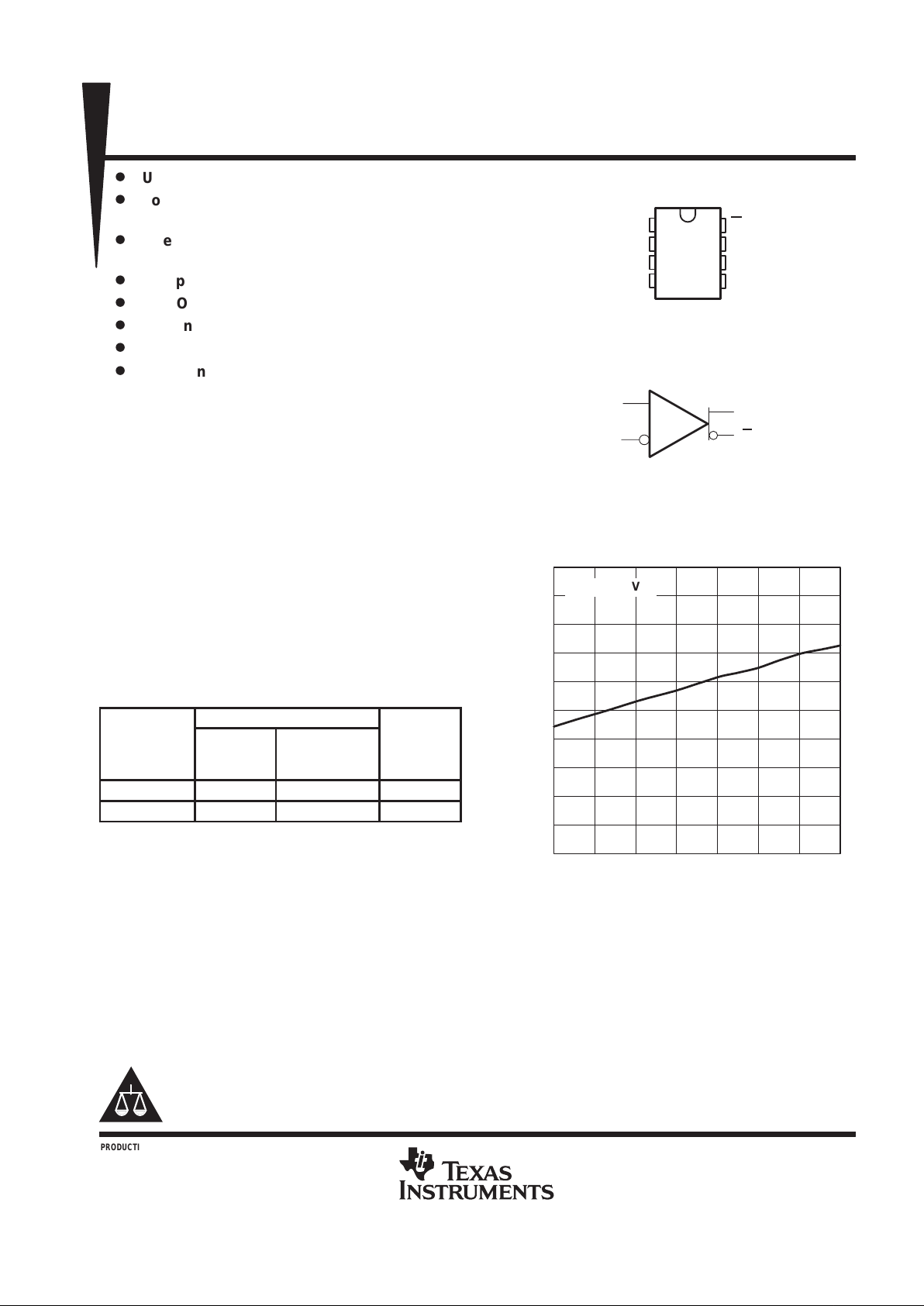
The TL3016 is an ultrafast comparator designed
to interface directly to TTL logic while operating
from either a single 5-V power supply or dual
±5-V supplies. It features extremely tight offset
voltage and high gain for precision applications. It
has complementary outputs that can be latched
using the LATCH ENABLE terminal. Figure 1
shows the positive supply current of this
comparator. The TL3016 only requires 10.6 mA
(typical) to achieve a propagation delay of 7.6 ns.
The TL3016 is a pin-for-pin functional replacement for the LT1016 comparator, offering higher
speed operation but consuming half the power.
AVAILABLE OPTIONS
PACKAGED DEVICES
T
A
SMALL
OUTLINE
†
(D)
TSSOP
(PW)
CHIP
FORM
‡
(Y)
0°C to 70°C TL3016CD TL3016CPWLE TL3016Y
–40°C to 85°C TL3016ID TL3016IPWLE —
†
The PW packages are available left-ended taped and reeled only.
‡
Chip forms are tested at TA = 25°C only.
Please be aware that an important notice concerning availability, standard warranty, and use in critical applications of
Texas Instruments semiconductor products and disclaimers thereto appears at the end of this data sheet.
1
2
3
4
8
7
6
5
V
CC+
IN+
IN–
V
CC–
Q OUT
Q OUT
GND
LATCH ENABLE
D AND PW PACKAGE
(TOP VIEW)
Figure 1
– 50 – 25 0 25 50 75 100 125
9
7
6
13
14
POSITIVE SUPPLY CURRENT
vs
FREE-AIR TEMPERATURE
15
12
11
8
5
10
– Positive Supply Current – mA
I
CC
TA – Free-Air Temperature – °C
symbol (each comparator)
IN+
IN–
Q
OUT
Q OUT
VCC = ± 5 V
PRODUCTION DATA information is current as of publication date.
Products conform to specifications per the terms of Texas Instruments
standard warranty. Production processing does not necessarily include
testing of all parameters.
Copyright 2000, Texas Instruments Incorporated
TL3016, TL3016Y
ULTRA-FAST LOW-POWER
PRECISION COMPARATORS
SLCS130D – MARCH 1997 – REVISED MARCH 2000
2
POST OFFICE BOX 655303 • DALLAS, TEXAS 75265
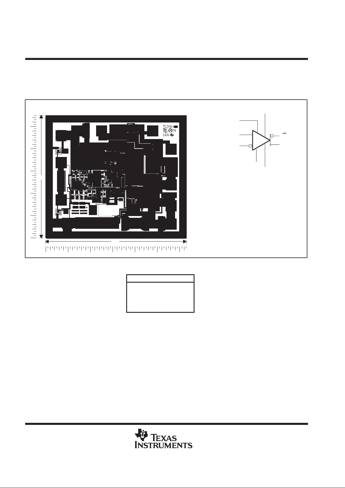
TL3016Y chip information
This chip displays characteristics similar to the TL3016C. Thermal compression or ultrasonic bonding may be
used on the doped-aluminum bonding pads. Chips may be mounted with conductive epoxy or a gold-silicon
preform.
BONDING PAD ASSIGNMENTS
CHIP THICKNESS: 10 MILS TYPICAL
BONDING PADS: 4 × 4 MILS MINIMUM
TJ max = 150°C
TOLERANCES ARE ±10%.
ALL DIMENSIONS ARE IN MILS.
TERMINALS 1 AND 6 CAN BE
CONNECTED TO MULTIPLE PADS.
Q OUT
IN–
IN+
LATCH ENABLE
Q OUT
(5)
(2)
(3)
(1)
(6)
V
CC+
GND
(7)
(8)
+
–
55
63
V
CC–
(4)
(1)
(4)
(3)
(2)
(5)
(1)
(1)
(8)
(7)
(6)
(6)
(6)
COMPONENT COUNT
Bipolars 53
MOSFETs 49
Resistors 46
Capacitors 14
TL3016, TL3016Y
ULTRA-FAST LOW-POWER
PRECISION COMPARATORS
SLCS130D – MARCH 1997 – REVISED MARCH 2000
3
POST OFFICE BOX 655303 • DALLAS, TEXAS 75265
absolute maximum ratings over operating free-air temperature range (unless otherwise noted)
†
Supply voltage, VDD (see Note 1) – 7 V to 7 V. . . . . . . . . . . . . . . . . . . . . . . . . . . . . . . . . . . . . . . . . . . . . . . . . . . . . .
Differential input voltage, VID (see Note 2) 7 V. . . . . . . . . . . . . . . . . . . . . . . . . . . . . . . . . . . . . . . . . . . . . . . . . . . . .
Input voltage range, VI 7 V. . . . . . . . . . . . . . . . . . . . . . . . . . . . . . . . . . . . . . . . . . . . . . . . . . . . . . . . . . . . . . . . . . . . . . .
Input voltage, V
I
(LA TCH ENABLE) 7 V. . . . . . . . . . . . . . . . . . . . . . . . . . . . . . . . . . . . . . . . . . . . . . . . . . . . . . . . . . . .
Output current, IO ± 20 mA. . . . . . . . . . . . . . . . . . . . . . . . . . . . . . . . . . . . . . . . . . . . . . . . . . . . . . . . . . . . . . . . . . . . . . .
Continuous total power dissipation See Dissipation Rating Table. . . . . . . . . . . . . . . . . . . . . . . . . . . . . . . . . . . . .
Operating free-air temperature range, TA –40°C to 85°C. . . . . . . . . . . . . . . . . . . . . . . . . . . . . . . . . . . . . . . . . . . .
Storage temperature range, T
stg
– 65°C to 150°C. . . . . . . . . . . . . . . . . . . . . . . . . . . . . . . . . . . . . . . . . . . . . . . . . .
Lead temperature 1,6 mm (1/16 inch) from case for 10 seconds 260°C. . . . . . . . . . . . . . . . . . . . . . . . . . . . . . .
†
Stresses beyond those listed under “absolute maximum ratings” may cause permanent damage to the device. These are stress ratings only, and
functional operation of the device at these or any other conditions beyond those indicated under “recommended operating conditions” is not
implied. Exposure to absolute-maximum-rated conditions for extended periods may affect device reliability.
NOTES: 1. All voltage values, except differential voltages, are with respect to network ground.
2. Differential voltages are at IN+ with respect to IN–.
DISSIPATION RATING TABLE
PACKAGE
TA ≤ 25°C
POWER RATING
DERATING FACTOR
ABOVE TA = 25°C
TA = 70°C
POWER RATING
D 725 mW 5.8 mW/°C 464 mW
PW
525 mW 4.2 mW/°C 336 mW
TL3016, TL3016Y
ULTRA-FAST LOW-POWER
PRECISION COMPARATORS
SLCS130D – MARCH 1997 – REVISED MARCH 2000
4
POST OFFICE BOX 655303 • DALLAS, TEXAS 75265
electrical characteristics at specified operating free-air temperature, VDD = ±5 V, VLE = 0 (unless
otherwise noted)
TL3016C TL3016I
PARAMETER
TEST CONDITIONS
†
MIN TYP‡MAX MIN TYP‡MAX
UNIT
p
TA = 25°C 0.5 3 0.5 3
VIOInput offset voltage
TA = full range 3.5 3.5
mV
α
VIO
T emperature coef ficient of
input offset voltage
–4.8 –4.5 µV/°C
p
TA = 25°C 0.1 0.6 0.1 0.6
IIOInput offset current
TA = full range 0.9 1.3
µ
A
p
TA = 25°C 6 10 6 10
IIBInput bias current
TA = full range 10 10
µ
A
Common-mode input
VDD = ±5 V –3.75 3.5 –3.75 3.5
V
ICR
voltage range
VDD = 5 V
1.25 3.5 1.25 3.5
V
CMRR
Common-mode rejection
ratio
–3.75 ≤ VIC ≤ 3.5 V, TA = 25°C 80 97 80 97 dB
Supply-voltage rejection
Positive supply: 4.6 V ≤ +VDD ≤ 5.4 V,
TA = 25°C
60 72 60 72
k
SVR
ygj
ratio
Negative supply: –7 V ≤ –VDD ≤ –2 V,
TA = 25°C
80 100 80 100
dB
p
I
(sink)
= 4 mA,
TA = 25°C
V+ ≤ 4.6 V,
500 600 500 600
VOLLow-level output voltage
I
(sink)
= 10 mA,
TA = 25°C
V+ ≤ 4.6 V,
750 750
mV
p
V+ ≤ 4.6 V,
TA = 25°C
IO = 1 mA,
3.6 3.9 3.6 3.9
VOHHigh-level output voltage
V+ ≤ 4.6 V,
TA = 25°C
IO = 10 mA,
3.4 3.7 3.4 3.7
V
Positive supply current
10.6 12.5 10.6 12.5
I
DD
Negative supply current
T
A
= full
range
–1.8 –1.3 –2.4 –1.3
mA
V
IL
Low-level input voltage
(LATCH ENABLE)
0.8 0.8 V
V
IH
High-level input voltage
(LATCH ENABLE)
2 2 V
Low-level input current
VLE = 0 0 1 0 1
I
IL
(LATCH ENABLE)
VLE = 2 V 24 39 24 45
µA
†
Full range for the TL3016C is TA = 0°C to 70°C. Full range for the TL3016I is TA = –40°C to 85°C.
‡
All typical values are measures with TA = 25°C.

TL3016, TL3016Y
ULTRA-FAST LOW-POWER
PRECISION COMPARATORS
SLCS130D – MARCH 1997 – REVISED MARCH 2000
5
POST OFFICE BOX 655303 • DALLAS, TEXAS 75265
switching characteristics, VDD = ±5 V, VLE = 0 (unless otherwise noted)
TL3016C TL3016I
PARAMETER
TEST CONDITIONS
†
MIN TYP MAX MIN TYP MAX
UNIT
∆V
= 100 mV ,
TA = 25°C 7.8 10 7.8 10
I
,
VOD = 5 mV
TA = full range 7.8 11.2 7.8 12.2
t
pd1
P
ropagation delay time
‡
∆V
= 100 mV ,
TA = 25°C 7.6 10 7.6 10
ns
I
,
VOD = 20 mV
TA = full range 7.6 11.2 7.6 12.2
t
sk(p)
Pulse skew (|t
pd+
– t
pd–
|)
∆VI = 100 mV ,
TA = 25°C
VOD = 5 mV,
0.5 0.5 ns
t
su
Setup time, LATCH ENABLE 2.5 2.5 ns
†
Full range for the TL3016C is 0°C to 70°C. Full range for the TL3016I is –40°C to 85°C.
‡
t
pd1
cannot be measured in automatic handling equipment with low values of overdrive. The TL3016 is 100% tested with a 1-V step and 500-mV
overdrive at TA = 25°C only. Correlation tests have shown that t
pd1
limits given can be ensured with this test, if additional dc tests are performed
to ensure that all internal bias conditions are correct. For low overdrive conditions, VOS is added to the overdrive.
TYPICAL CHARACTERISTICS
Table of Graphs
FIGURE
vs Input voltage 2
I
CC
Positive supply current
vs Frequency
3
vs Free-air temperature 4
I
CC
Negative supply current vs Free-air temperature 5
vs Overdrive voltage 6
vs Supply voltage 7
t
pd
Propagation delay time
vs Input impedance
8
vs Load capacitance 9
vs Free-air temperature 10
V
IC
Common-mode input voltage vs Free-air temperature 11
Input threshold voltage (LATCH ENABLE) vs Free-air temperature 12
p
vs Output source current 13
VOOutput voltage
vs Output sink current 14
I
I
Input current (LATCH ENABLE) vs Input voltage 15

TL3016, TL3016Y
ULTRA-FAST LOW-POWER
PRECISION COMPARATORS
SLCS130D – MARCH 1997 – REVISED MARCH 2000
6
POST OFFICE BOX 655303 • DALLAS, TEXAS 75265
TYPICAL CHARACTERISTICS
Figure 2
POSITIVE SUPPLY CURRENT
vs
INPUT VOLTAGE
– Positive Supply Current – mA
I
CC
20
18
16
14
12
10
8
6
4
2
0
12345678
TA = –40°C
TA = 85°C
TA = 25°C
VI – Input Voltage – V
VCC = ± 5 V
TA = 25°C
Figure 3
18
16
12
10
8
22
14
– Positive Supply Current – mA
20
f – Frequency – MHz
POSITIVE SUPPLY CURRENT
vs
FREQUENCY
010110
2
I
CC
TA = –40°C
TA = 85°C
TA = 25°C
VCC = ± 5 V
TA = 25°C
Figure 4
– 50 – 25 0 25 50 75 100 125
9
7
6
13
14
POSITIVE SUPPLY CURRENT
vs
FREE-AIR TEMPERATURE
15
12
11
8
5
10
– Positive Supply Current – mA
I
CC
TA – Free-Air Temperature – °C
VCC = ± 5 V
Figure 5
– 1.5
– 2.5
– 3
– 50 – 25 0 25 50
– 1
NEGATIVE SUPPLY CURRENT
vs
FREE-AIR TEMPERATURE
0
75 100 125
– 0.5
– 2
– Negative Supply Current – mA
I
CC
TA – Free-Air Temperature – °C
VCC = ± 5 V

TL3016, TL3016Y
ULTRA-FAST LOW-POWER
PRECISION COMPARATORS
SLCS130D – MARCH 1997 – REVISED MARCH 2000
7
POST OFFICE BOX 655303 • DALLAS, TEXAS 75265
TYPICAL CHARACTERISTICS
Figure 6
4
3
1
0
0102030
– Propagation Delay Time – ns
6
7
Overdrive Voltage – mV
PROPAGATION DELAY TIME
vs
OVERDRIVE VOLTAGE
8
40 50
5
2
t
pd
9
10
VCC = ± 5 V
TA = 25°C
Figure 7
Falling Edge
Rising Edge
6
4
0
4.4 4.6 4.8 5
8
10
PROPAGATION DELAY TIME
vs
SUPPLY VOLTAGE
12
5.2 5.4 5.6
– Propagation Delay Time – nst
pd
VCC – Supply Voltage – V
2
VCC = ± 5 V
TA = 25°C
Figure 8
5 mV
20 mV
10
6
4
0
0 50 100 150
14
18
PROPAGATION DELAY TIME
vs
INPUT IMPEDANCE
20
200 250 300
16
12
8
2
– Propagation Delay Time – nst
pd
ZO – Input Impedance – Ω
VCC = ± 5 V
TA = 25°C
Figure 9
t
PDHL
t
PDLH
CL – Load Capacitance – pF
5
4
2
0
010 2030
7
9
PROPAGATION DELAY TIME
vs
LOAD CAPACITANCE
10
40 50
8
6
3
1
– Propagation Delay Time – nst
pd
VCC = ± 5 V
TA = 25°C

TL3016, TL3016Y
ULTRA-FAST LOW-POWER
PRECISION COMPARATORS
SLCS130D – MARCH 1997 – REVISED MARCH 2000
8
POST OFFICE BOX 655303 • DALLAS, TEXAS 75265
TYPICAL CHARACTERISTICS
Figure 10
TA – Free-Air Temperature – °C
Rising Edge
Falling Edge
10
5
0
– 50 – 25 0 25 50
– Propagation Delay Time – ns
15
20
PROPAGATION DELAY TIME
vs
FREE-AIR TEMPERATURE
25
75 100 125
t
pd
VCC = ± 5 V
Figure 11
0
–2
–4
–6
– 50 – 25 0 25 50
– Common-Mode Input Voltage – V
2
4
COMMON-MODE INPUT VOLTAGE
vs
FREE-AIR TEMPERATURE
6
75 100 125
TA – Free-Air Temperature – °C
V
IC
VCC = 5 V (Upper Limit)
VCC = ± 5 V (Upper Limit)
VCC = 5 V (Lower Limit)
VCC = ± 5 V (Lower Limit)
Figure 12
TA – Free-Air Temperature – °C
1
0.6
0.4
0
–50 –25 0 25 50
1.6
1.8
2
75 100 125 150
1.4
1.2
0.8
0.2
VCC = ± 5 V
INPUT THRESHOLD VOLTAGE (LATCH ENABLE)
vs
FREE-AIR TEMPERATURE
– Input Threshold Voltage (LATCH ENABLE) – V
V
IT
Figure 13
3.8
0510
4.6
4.8
5
15 20
– Output Voltage – V
OUTPUT VOLTAGE
vs
OUTPUT SOURCE CURRENT
V
O
I
O(source)
– Output Source Current – mA
TA = –40°C
TA = 85°C
TA = 25°C
4.4
4.2
4
3.6
3.4
3.2
3
VCC = ± 5 V
TA = 25°C

TL3016, TL3016Y
ULTRA-FAST LOW-POWER
PRECISION COMPARATORS
SLCS130D – MARCH 1997 – REVISED MARCH 2000
9
POST OFFICE BOX 655303 • DALLAS, TEXAS 75265
TYPICAL CHARACTERISTICS
Figure 14
TA = –40°C
TA = 25°C
TA = 85°C
VCC = ± 5 V
TA = 25°C
1
0.6
0.4
0
0510
– Output Voltage – V
1.4
1.6
OUTPUT VOLTAGE
vs
OUTPUT SINK CURRENT
2
15 20
1.8
1.2
0.8
0.2
V
O
I
O(sink)
– Output Sink Current – mA
Figure 15
5
– 5
– 10
– 20
– 0.5 0 0.5 1
15
25
INPUT CURRENT (LATCH ENABLE)
vs
INPUT VOLTAGE
30
1.5 2
20
10
0
– 15
VI – Input Voltage – V
– Input Current (LATCH ENABLE) –I
I
Aµ
VCC = ± 5 V
TA = 25°C

TL3016, TL3016Y
ULTRA-FAST LOW-POWER
PRECISION COMPARATORS
SLCS130D – MARCH 1997 – REVISED MARCH 2000
10
POST OFFICE BOX 655303 • DALLAS, TEXAS 75265
MECHANICAL INFORMATION
D (R-PDSO-G**) PLASTIC SMALL-OUTLINE PACKAGE
14 PIN SHOWN
4040047/B 03/95
0.228 (5,80)
0.244 (6,20)
0.069 (1,75) MAX
0.010 (0,25)
0.004 (0,10)
1
14
0.014 (0,35)
0.020 (0,51)
A
0.157 (4,00)
0.150 (3,81)
7
8
0.044 (1,12)
0.016 (0,40)
Seating Plane
0.010 (0,25)
PINS **
0.008 (0,20) NOM
A MIN
A MAX
DIM
Gage Plane
0.189
(4,80)
(5,00)
0.197
8
(8,55)
(8,75)
0.337
14
0.344
(9,80)
16
0.394
(10,00)
0.386
0.004 (0,10)
M
0.010 (0,25)
0.050 (1,27)
0°–8°
NOTES: A. All linear dimensions are in inches (millimeters).
B. This drawing is subject to change without notice.
C. Body dimensions do not include mold flash or protrusion, not to exceed 0.006 (0,15).
D. Four center pins are connected to die mount pad.
E. Falls within JEDEC MS-012

TL3016, TL3016Y
ULTRA-FAST LOW-POWER
PRECISION COMPARATORS
SLCS130D – MARCH 1997 – REVISED MARCH 2000
11
POST OFFICE BOX 655303 • DALLAS, TEXAS 75265
MECHANICAL INFORMATION
PW (R-PDSO-G**) PLASTIC SMALL-OUTLINE PACKAGE
4040064/D 10/95
14 PIN SHOWN
Seating Plane
0,10 MIN
1,20 MAX
1
A
7
14
0,19
4,50
4,30
8
6,10
6,70
0,32
0,75
0,50
0,25
Gage Plane
0,15 NOM
0,65
M
0,13
0°–8°
0,10
PINS **
A MIN
A MAX
DIM
2,90
3,10
8
4,90
5,10
14
6,60
6,404,90
5,10
16
7,70
20
7,90
24
9,60
9,80
28
NOTES: A. All linear dimensions are in millimeters.
B. This drawing is subject to change without notice.
C. Body dimensions do not include mold flash or protrusion not to exceed 0,15.
D. Falls within JEDEC MO-153

IMPORTANT NOTICE
T exas Instruments and its subsidiaries (TI) reserve the right to make changes to their products or to discontinue
any product or service without notice, and advise customers to obtain the latest version of relevant information
to verify, before placing orders, that information being relied on is current and complete. All products are sold
subject to the terms and conditions of sale supplied at the time of order acknowledgement, including those
pertaining to warranty, patent infringement, and limitation of liability.
TI warrants performance of its semiconductor products to the specifications applicable at the time of sale in
accordance with TI’s standard warranty. Testing and other quality control techniques are utilized to the extent
TI deems necessary to support this warranty. Specific testing of all parameters of each device is not necessarily
performed, except those mandated by government requirements.
CERT AIN APPLICATIONS USING SEMICONDUCTOR PRODUCTS MAY INVOLVE POTENTIAL RISKS OF
DEATH, PERSONAL INJURY, OR SEVERE PROPERTY OR ENVIRONMENTAL DAMAGE (“CRITICAL
APPLICATIONS”). TI SEMICONDUCTOR PRODUCTS ARE NOT DESIGNED, AUTHORIZED, OR
WARRANTED TO BE SUITABLE FOR USE IN LIFE-SUPPORT DEVICES OR SYSTEMS OR OTHER
CRITICAL APPLICATIONS. INCLUSION OF TI PRODUCTS IN SUCH APPLICA TIONS IS UNDERSTOOD T O
BE FULLY AT THE CUSTOMER’S RISK.
In order to minimize risks associated with the customer’s applications, adequate design and operating
safeguards must be provided by the customer to minimize inherent or procedural hazards.
TI assumes no liability for applications assistance or customer product design. TI does not warrant or represent
that any license, either express or implied, is granted under any patent right, copyright, mask work right, or other
intellectual property right of TI covering or relating to any combination, machine, or process in which such
semiconductor products or services might be or are used. TI’s publication of information regarding any third
party’s products or services does not constitute TI’s approval, warranty or endorsement thereof.
Copyright 2000, Texas Instruments Incorporated
 Loading...