

www.ti.com
FEATURES
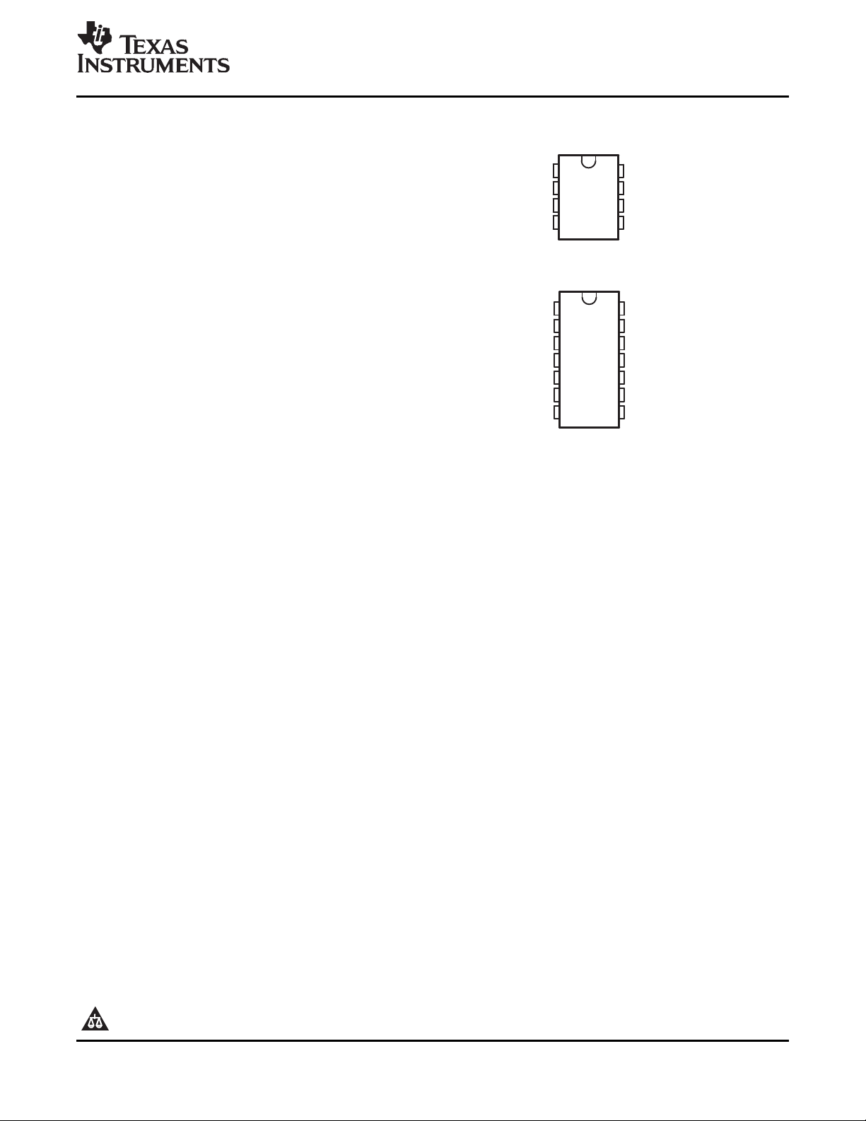
1
2
3
4
8
7
6
5
COMP
VFB
I
SENSE
RT/C
T
V
REF
V
CC
OUTPUT
GND
D (SOIC) OR P (PDIP) PACKAGE
(TOP VIEW)
1
2
3
4
5
6
7
14
13
12
11
10
9
8
COMP
NC
VFB
NC
I
SENSE
NC
RT/C
T
V
REF
NC
V
CC
VC
OUTPUT
GND
POWER GROUND
D (SOIC) PACKAGE
(TOP VIEW)
NC − No internal connection
• Low Start-Up Current (<0.5 mA)
• Trimmed Oscillator Discharge Current
• Current Mode Operation to 500 kHz
• Automatic Feed-Forward Compensation
• Latching PWM for Cycle-by-Cycle Current
Limiting
• Internally Trimmed Reference With
Undervoltage Lockout
• High-Current Totem-Pole Output Undervoltage
Lockout With Hysteresis
• Double-Pulse Suppression
TL284xB , TL384xB
HIGH-PERFORMANCE CURRENT-MODE PWM CONTROLLERS
SLVS610B – AUGUST 2006 – REVISED JULY 2007
DESCRIPTION/ORDERING INFORMATION
The TL284xB and TL384xB series of control integrated circuits provide the features that are necessary to
implement off-line or dc-to-dc fixed-frequency current-mode control schemes, with a minimum number of
external components. Internally implemented circuits include an undervoltage lockout (UVLO) and a precision
reference that is trimmed for accuracy at the error amplifier input. Other internal circuits include logic to ensure
latched operation, a pulse-width modulation (PWM) comparator that also provides current-limit control, and a
totem-pole output stage designed to source or sink high-peak current. The output stage, suitable for driving
N-channel MOSFETs, is low when it is in the off state.
The TL284xB and TL384xB series are pin compatible with the standard TL284x and TL384x with the following
improvements. The start-up current is specified to be 0.5 mA (max), while the oscillator discharge current is
trimmed to 8.3 mA (typ). In addition, during undervoltage lockout conditions, the output has a maximum
saturation voltage of 1.2 V while sinking 10 mA (V
Major differences between members of these series are the UVLO thresholds and maximum duty-cycle ranges.
Typical UVLO thresholds of 16 V (on) and 10 V (off) on the TLx842B and TLx844B devices make them ideally
suited to off-line applications. The corresponding typical thresholds for the TLx843B and TLx845B devices are
8.4 V (on) and 7.6 V (off). The TLx842B and TLx843B devices can operate to duty cycles approaching 100%. A
duty-cycle range of 0% to 50% is obtained by the TLx844B and TLx845B by the addition of an internal toggle
flip-flop, which blanks the output off every other clock cycle.The TL284xB-series devices are characterized for
operation from –40 ° C to 85 ° C. The TL384xB-series devices are characterized for operation from 0 ° C to 70 ° C.
= 5 V).
CC
PRODUCTION DATA information is current as of publication date.
Products conform to specifications per the terms of the Texas
Instruments standard warranty. Production processing does not
necessarily include testing of all parameters.
Please be aware that an important notice concerning availability, standard warranty, and use in critical applications of Texas
Instruments semiconductor products and disclaimers thereto appears at the end of this data sheet.
Copyright © 2006–2007, Texas Instruments Incorporated
www.ti.com
TL284xB , TL384xB
HIGH-PERFORMANCE CURRENT-MODE PWM CONTROLLERS
SLVS610B – AUGUST 2006 – REVISED JULY 2007
ORDERING INFORMATION
T
A
PDIP – P Tube of 50
SOIC – D (8 pin)
–40 ° C to 85 ° C
SOIC – D (14 pin)
PDIP – P Tube of 50
SOIC – D (8 pin)
0 ° C to 70 ° C
SOIC – D (14 pin)
(1) Package drawings, standard packing quantities, thermal data, symbolization, and PCB design guidelines are available at
www.ti.com/sc/package.
PACKAGE
(1)
Tube of 75 TL2842BD-8
Reel of 2500 TL2842BDR-8
Tube of 75 TL2843BD-8
Reel of 2500 TL2843BDR-8
Tube of 75 TL2844BD-8
Reel of 2500 TL2844BDR-8
Tube of 75 TL2845BD-8
Reel of 2500 TL2845BDR-8
Tube of 75 TL2842BD
Reel of 2500 TL2842BDR
Tube of 75 TL2843BD
Reel of 2500 TL2843BDR
Tube of 75 TL2844BD
Reel of 2500 TL2844BDR
Tube of 75 TL2845BD
Reel of 2500 TL2845BDR
Tube of 75 TL3842BD-8
Reel of 2500 TL3842BDR-8
Tube of 75 TL3843BD-8
Reel of 2500 TL3843BDR-8
Tube of 75 TL3844BD-8
Reel of 2500 TL3844BDR-8
Tube of 75 TL3845BD-8
Reel of 2500 TL3845BDR-8
Tube of 75 TL3842BD
Reel of 2500 TL3842BDR
Tube of 75 TL3843BD
Reel of 2500 TL3843BDR
Tube of 75 TL3844BD
Reel of 2500 TL3844BDR
Tube of 75 TL3845BD
Reel of 2500 TL3845BDR
ORDERABLE PART NUMBER TOP-SIDE MARKING
TL2842BP TL2842BP
TL2843BP TL2843BP
TL2844BP TL2844BP
TL2845BP TL2845BP
2842B
2843B
2844B
2845B
TL2842B
TL2843B
TL2844B
TL2845B
TL3842BP TL3842BP
TL3843BP TL3843BP
TL3844BP TL3844BP
TL3845BP TL3845BP
3842B
3843B
3844B
3845B
TL3842B
TL3843B
TL3844B
TL3845B
2
Submit Documentation Feedback
www.ti.com
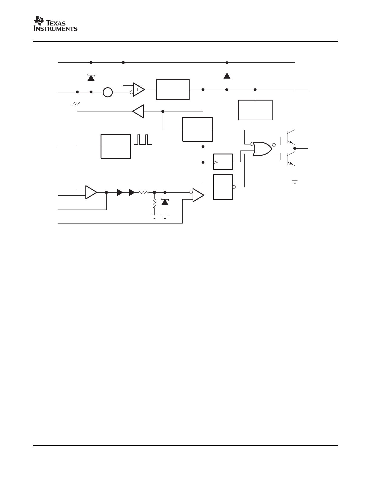
Internal
Bias
V
REF
Good
Logic
OSC
Error
Amplifier
PWM
Latch
Current-
Sense
Comparator
34 V NOM
V
CC
GND
RT/C
T
VFB
COMP
I
SENSE
7
5
4
2
1
3
8
6
V
REF
OUTPUT
+
−
UVLO
EN
2R
R 1 V
S
R
T
+
−
5-V V
REF
2.5 V
HIGH-PERFORMANCE CURRENT-MODE PWM CONTROLLERS
FUNCTIONAL BLOCK DIAGRAM
TL284xB , TL384xB
SLVS610B – AUGUST 2006 – REVISED JULY 2007
A. Pin numbers shown are for the 8-pin D package.
Submit Documentation Feedback
3
www.ti.com
TL284xB , TL384xB
HIGH-PERFORMANCE CURRENT-MODE PWM CONTROLLERS
SLVS610B – AUGUST 2006 – REVISED JULY 2007
Absolute Maximum Ratings
over operating free-air temperature range (unless otherwise noted)
V
CC
V
I
I
CC
I
O
I
O(sink)
θ
JA
T
J
T
stg
T
lead
(1) Stresses beyond those listed under "absolute maximum ratings" may cause permanent damage to the device. These are stress ratings
(2) All voltages are with respect to the device GND terminal.
(3) Maximum power dissipation is a function of TJ(max), θJA, and TA. The maximum allowable power dissipation at any allowable ambient
(4) The package thermal impedance is calculated in accordance with JESD 51-7.
Supply voltage V
Analog input voltage range VFB and I
Supply current 30 mA
Output current ± 1 A
Error amplifier output sink current 10 mA
Package thermal impedance
Output energy Capacitive load 5 μ J
Virtual junction temperature 150 ° C
Storage temperature range –65 150 ° C
Lead temperature Soldering, 10 s 300 ° C
only, and functional operation of the device at these or any other conditions beyond those indicated under "recommended operating
conditions" is not implied. Exposure to absolute-maximum-rated conditions for extended periods may affect device reliability.
temperature is PD= (TJ(max) – TA)/ θJA. Operating at the absolute maximum TJof 150 ° C can impact reliability.
(1) (2)
MIN MAX UNIT
Low impedance source 30
ICC< 30 mA
SENSE
(3) (4)
D package
8 pin 97
14 pin 86 ° C/W
limiting
–0.3 6.3 V
P package 85
Self
Recommended Operating Conditions
V
V
CC
V
I
V
O
I
CC
I
O
I
O(ref)
f
osc
T
J
Supply voltage V
Input voltage V
Output voltage V
Supply current, externally limited 25 mA
Average output current 200 mA
Reference output current –20 mA
Oscillator frequency 100 500 kHz
Operating free-air temperature ° C
(1) The recommended voltages for VC and POWER GROUND apply only to the 14-pin D package.
CC
(1)
VC
RT/C
T
VFB and I
SENSE
OUTPUT 0 30
POWER GROUND
TL284xB –40 85
TL384xB 0 70
MIN NOM MAX UNIT
30
30
0 5.5
0 5.5
(1)
–0.1 1
4
Submit Documentation Feedback
www.ti.com
HIGH-PERFORMANCE CURRENT-MODE PWM CONTROLLERS
TL284xB , TL384xB
SLVS610B – AUGUST 2006 – REVISED JULY 2007
Reference Section Electrical Characteristics
V
CC
Output voltage IO= 1 mA, TJ= 25 ° C 4.95 5 5.05 4.9 5 5.1 V
Line regulation V
Load regulation IO= 1 mA to 20 mA 6 25 6 25 mV
Average temperature
coefficient of output voltage
Output voltage, worst-case V
variation IO= 1 mA to 20 mA
Output noise voltage f = 10 Hz to 10 kHz, TJ= 25 ° C 50 50 μ V
Output-voltage long-term drift After 1000 h at TJ= 25 ° C 5 25 5 25 mV
Short-circuit output current –30 –100 –180 –30 –100 –180 mA
(1) Adjust V
(2) All typical values are at TJ= 25 ° C.
Oscillator Section
V
CC
Initial accuracy kHz
Voltage stability V
Temperature stability 5 5 %
Amplitude Peak to peak 1.7 1.7 V
Discharge current mA
(1) Output frequency equals oscillator frequency for the TL3842B and TL3843B. Output frequency is one-half the oscillator frequency for the
(2) Adjust V
(3) All typical values are at TJ= 25 ° C.
(1)
= 15 V
, RT= 10 k Ω , CT= 3.3 nF, over recommended operating free-air temperature range (unless otherwise specified)
PARAMETER TEST CONDITIONS UNIT
= 12 V to 25 V 6 20 6 20 mV
CC
TL284xB TL384xB
MIN TYP
(2)
MAX MIN TYP
(2)
0.2 0.4 0.2 0.4 mV/ ° C
= 12 V to 25 V,
CC
above the start threshold before setting it to 15 V.
CC
(1)
Electrical Characteristics
= 15 V
(2)
, RT= 10 k Ω , CT= 3.3 nF, over recommended operating free-air temperature range (unless otherwise specified)
PARAMETER TEST CONDITIONS UNIT
4.9 5.1 4.82 5.18 V
TL284xB TL384xB
MIN TYP
(3)
MAX MIN TYP
(3)
TJ= 25 ° C 49 52 55 49 52 55
TA= T
TJ= 25 ° C, RT= 6.2 k Ω ,
CT= 1 nF
TJ= 25 ° C, RT/C
RT/C
to T
low
high
48 56 48 56
225 250 275 225 250 275
= 12 V to 25 V 0.2 1 0.2 1 %
CC
= 2 V 7.8 8.3 8.8 7.8 8.3 8.8
T
= 2 V 7.5 8.8 7.6 8.8
T
TL3844B and TL3845B.
above the start threshold before setting it to 15 V.
CC
MAX
MAX
Submit Documentation Feedback
5
www.ti.com
TL284xB , TL384xB
HIGH-PERFORMANCE CURRENT-MODE PWM CONTROLLERS
SLVS610B – AUGUST 2006 – REVISED JULY 2007
Error-Amplifier Section Electrical Characteristics
V
CC
Feedback input voltage COMP = 2.5 V 2.45 2.5 2.55 2.42 2.5 2.58 V
Input bias current –0.3 –1 –0.3 –2 μ A
Open-loop voltage
amplification
Gain-bandwidth product 0.7 1 0.7 1 MHz
Supply-voltage rejection ratio V
Output sink current VFB = 2.7 V, COMP = 1.1 V 2 6 2 6 mA
Output source current VFB = 2.3 V, COMP = 5 V –0.5 –0.8 –0.5 –0.8 mA
High-level output voltage 5 6 5 6 V
Low-level output voltage 0.7 1.1 0.7 1.1 V
(1) Adjust V
(2) All typical values are at TJ= 25 ° C.
(1)
= 15 V
, RT= 10 k Ω , CT= 3.3 nF, over recommended operating free-air temperature range (unless otherwise specified)
PARAMETER TEST CONDITIONS UNIT
TL284xB TL384xB
MIN TYP
(2)
MAX MIN TYP
(2)
VO= 2 V to 4 V 65 90 65 90 dB
= 12 V to 25 V 60 70 60 70 dB
CC
VFB = 2.3 V,
RL= 15 k Ω to GND
VFB = 2.7 V,
RL= 15 k Ω to GND
above the start threshold before setting it to 15 V.
CC
MAX
Current-Sense Section Electrical Characteristics
V
CC
Voltage amplification
Current-sense comparator
threshold
Supply-voltage rejection
ratio
Input bias current –2 –10 –2 –10 μ A
Delay time to output VFB = 0 V to 2 V 150 300 150 300 ns
(1) Adjust V
(2) All typical values are at TJ= 25 ° C.
(3) Measured at the trip point of the latch, with VFB at 0 V.
(4) Measured between I
(1)
= 15 V
(3)
, RT= 10 k Ω , CT= 3.3 nF, over recommended operating free-air temperature range (unless otherwise specified)
PARAMETER TEST CONDITIONS UNIT
(3) (4)
(3)
above the start threshold before setting it to 15 V.
CC
COMP = 5 V 0.9 1 1.1 0.9 1 1.1 V
V
= 12 V to 25 V 70 70 dB
CC
and COMP, with the input changing from 0 V to 0.8 V.
SENSE
TL284xB TL384xB
MIN TYP
(2)
MAX MIN TYP
(2)
2.85 3 3.15 2.85 3 3.15 V/V
MAX
6
Submit Documentation Feedback
www.ti.com
HIGH-PERFORMANCE CURRENT-MODE PWM CONTROLLERS
TL284xB , TL384xB
SLVS610B – AUGUST 2006 – REVISED JULY 2007
Output Section Electrical Characteristics
V
CC
High-level output voltage V
Low-level output voltage V
Rise time CL= 1 nF, TJ= 25 ° C 50 150 50 150 ns
Fall time CL= 1 nF, TJ= 25 ° C 50 150 50 150 ns
UVLO saturation V
(1) Adjust V
(2) All typical values are at TJ= 25 ° C.
(1)
= 15 V
, RT= 10 k Ω , CT= 3.3 nF, over recommended operating free-air temperature range (unless otherwise specified)
PARAMETER TEST CONDITIONS UNIT
TL284xB TL384xB
MIN TYP
(2)
MAX MIN TYP
(2)
IOH= –20 mA 13 13.5 13 13.5
IOH= –200 mA 12 13.5 12 13.5
IOL= 20 mA 0.1 0.4 0.1 0.4
IOL= 200 mA 1.5 2.2 1.5 2.2
= 5 V, IOL= 1 mA 0.7 1.2 0.7 1.2 V
CC
above the start threshold before setting it to 15 V.
CC
MAX
Undervoltage-Lockout Section Electrical Characteristics
V
CC
Start threshold voltage V
Minimum operating voltage
after start-up
(1) Adjust V
(2) All typical values are at TJ= 25 ° C.
(1)
= 15 V
, RT= 10 k Ω , CT= 3.3 nF, over recommended operating free-air temperature range (unless otherwise specified)
PARAMETER TEST CONDITIONS UNIT
TL284xB TL384xB
MIN TYP
(2)
MAX MIN TYP
(2)
TLx842B, TLx844B 15 16 17 14.5 16 17.5
TLx843B, TLx845B 7.8 8.4 9 7.8 8.4 9
TLx842B, TLx844B 9 10 11 8.5 10 11.5
TLx843B, TLx845B 7 7.6 8.2 7 7.6 8.2
above the start threshold before setting it to 15 V.
CC
MAX
V
Pulse-Width Modulator Section Electrical Characteristics
V
CC
Maximum duty cycle %
Minimum duty cycle 0 0 %
(1) Adjust V
(2) All typical values are at TJ= 25 ° C.
(1)
= 15 V
, RT= 10 k Ω , CT= 3.3 nF, over recommended operating free-air temperature range (unless otherwise specified)
PARAMETER TEST CONDITIONS UNIT
TL284xB TL384xB
MIN TYP
(2)
MAX MIN TYP
(2)
TL3842B, TL3843B 94 96 100 94 96 100
TL3844B, TL3845B 47 48 50 47 48 50
above the start threshold before setting it to 15 V.
CC
MAX
Supply Voltage Electrical Characteristics
V
CC
Start-up current 0.3 0.5 0.3 0.5 mA
Operating supply current VFB and I
Limiting voltage ICC= 25 mA 30 34 30 34 V
(1) Adjust V
(2) All typical values are at TJ= 25 ° C.
(1)
= 15 V
, RT= 10 k Ω , CT= 3.3 nF, over recommended operating free-air temperature range (unless otherwise specified)
PARAMETER TEST CONDITIONS UNIT
at 0 V 11 17 11 17 mA
SENSE
above the start threshold before setting it to 15 V.
CC
TL284xB TL384xB
MIN TYP
(2)
MAX MIN TYP
(2)
MAX
Submit Documentation Feedback
7

www.ti.com
-20
0
20
40
60
80
100
1 . E +0 1 1 . E +0 2 1 . E +0 3 1 . E +0 4 1 . E +0 5 1 . E +0 6 1 . E +0 7
f – Frequency – Hz
A
VOL
– Open-Loop Voltage Gain – dB
-100
-50
0
50
100
150
200
Phase Margin – deg
VCC= 15V
RL= 100 kX
TA= 25°C
Phase
Gain
kΩ
10 100
1k
10k 100k
1M 10M
0
5
10
15
20
25
0 5 10 15 20 25 30 35 40
V
CC
– Supply Voltage – V
I
CC
– Supply Current – mA
TL2845
TL2842
0
0.2
0.4
0.6
0.8
1
1.2
0 1 2 3 4 5 6 7 8
V
O
– Error Amplifier Output Voltage – V
V
th
– Current-Sense Input Threshold – V
VIN= 15 V
TA= 125°C
TA= 25°C
TA= -55°C
7.4
7.6
7.8
8
8.2
8.4
8.6
8.8
9
9.2
-55 -35 -15 5 25 45 65 85 105 125 145
T
A
– Temperature – °C
I
disharge
– Oscillator Discharge Current – mA
VIN= 15 V
V
OSC
= 2 V
TL284xB , TL384xB
HIGH-PERFORMANCE CURRENT-MODE PWM CONTROLLERS
SLVS610B – AUGUST 2006 – REVISED JULY 2007
TYPICAL CHARACTERISTICS
SUPPLY CURRENT GAIN AND PHASE
ERROR AMPLIFIER OPEN-LOOP
vs vs
SUPPLY VOLTAGE FREQUENCY
CURRENT-SENSE INPUT THRESHOLD OSCILLATOR DISCHARGE CURRENT
ERROR AMPLIFIER OUTPUT VOLTAGE TEMPERATURE
8
vs vs
Submit Documentation Feedback

www.ti.com
-60
-50
-40
-30
-20
-10
0
0 20 40 60 80 100 120 140 160
I
src
– Source Current – mA
Reference Voltage Delta – mV
TA= -40°C
TA= 25°C
TA= 125°C
4.8
4.85
4.9
4.95
5
5.05
5.1
5.15
5.2
-55 -30 -5 20 45 70 95 120 145
T
A
– Temperature – °C
V
ref
– Reference Voltage – V
40
60
80
100
120
140
160
180
-55 -30 -5 20 45 70 95 120 145
T
A
– Temperature – °C
I
SC
– Short-Circuit Current – mA
VIN= 15 V
0
1
2
3
4
5
6
7
8
9
10
0 100 200 300 400 500 600 700 800
I
O
– Output Load Current – mA
Sink Saturation Voltage – V
-10
-9
-8
-7
-6
-5
-4
-3
-2
-1
0
Source Saturation
Sink Saturation
TA= 25°C
TA= -55°C
TA= -55°C
TA= 25°C
HIGH-PERFORMANCE CURRENT-MODE PWM CONTROLLERS
TYPICAL CHARACTERISTICS (continued)
TL284xB , TL384xB
SLVS610B – AUGUST 2006 – REVISED JULY 2007
REFERENCE VOLTAGE REFERENCE VOLTAGE
vs vs
SOURCE CURRENT TEMPERATURE
REFERENCE SHORT-CIRCUIT CURRENT OUTPUT SATURATION VOLTAGE
vs vs
TEMPERATURE LOAD CURRENT
Submit Documentation Feedback
9

www.ti.com
40
50
60
70
80
90
100
0.1 1 10
R
T
– Timing Resistor – k€
D
max
– Maximum Duty Cycle – %
VCC= 15 V
C
T
= 3.3 nF
T
A
= 25°C
kΩ
TL284xB , TL384xB
HIGH-PERFORMANCE CURRENT-MODE PWM CONTROLLERS
SLVS610B – AUGUST 2006 – REVISED JULY 2007
TYPICAL CHARACTERISTICS (continued)
MAXIMUM OUTPUT DUTY CYCLE
vs
TIMING RESISTOR
OUTPUT WAVEFORM
10
Submit Documentation Feedback

www.ti.com
Z
i
Z
f
VFB
COMP
2.5 V
0.5 mA
Error
Amplifier
+
−
R
S
C
f
R
f
Error
Amplifier
2R
R 1 V
Current-Sense
Comparator
I
S
(see Note A)
+
−
I
SENSE
COMP
GND
C
T
R
T
V
REF
RT/C
T
GND
HIGH-PERFORMANCE CURRENT-MODE PWM CONTROLLERS
APPLICATION INFORMATION
The error-amplifier configuation circuit is shown in Figure 1 .
A. Error amplifier can source or sink up to 0.5 mA.
Figure 1. Error-Amplifier Configuration
The current-sense circuit is shown in Figure 2 .
TL284xB , TL384xB
SLVS610B – AUGUST 2006 – REVISED JULY 2007
A. Peak current (IS) is determined by the formula: I
B. A small RC filter formed by resistor Rfand capacitor Cfmay be required to suppress switch transients.
= 1 V/R
S(max)
S
Figure 2. Current-Sense Circuit
The oscillator frequency is set using the circuit shown in Figure 3 . The frequency is calculated as:
For R
f = 1 / RTC
> 5 k Ω :
T
f ≈ 1.72 / RTC
T
T
Figure 3. Oscillator Section
Submit Documentation Feedback
11

www.ti.com
TIMING RESISTANCE
vs
FREQUENCY
Ω
100 1k 10k 100k 1M
f − Frequency − Hz
R
T
− Timing Resistance − k
100
40
10
4
1
VCC = 15 V
TA = 25°C
CT = 22 nF
CT = 47 nF
CT = 100 nF
CT = 10 nF
CT = 4.7 nF
CT = 2.2 nF
CT = 1 nF
DEAD TIME
vs
TIMING CAPACITANCE
sµ
100401041
CT − Timing Capacitance − nF
100
40
10
4
1
0.4
0.1
Dead Time −
VCC = 15 V
RT ≥ 5 kΩ
TA = 25°C
2N2222
4.7 kΩ
1-kΩ
Error Amplifier Adjust
4.7 kΩ
5 kΩ
I
SENSE
Adjust
R
T
100 kΩ
V
CC
0.1 µF
0.1 µF
REF
V
CC
OUTPUT
GND
1 kΩ, 1 W
A
C
T
TL284xB
TL384xB
I
SENSE
V
REF
RT/C
T
VFB
COMP
OUTPUT
GND
TL284xB , TL384xB
HIGH-PERFORMANCE CURRENT-MODE PWM CONTROLLERS
SLVS610B – AUGUST 2006 – REVISED JULY 2007
APPLICATION INFORMATION (continued)
Open-Loop Laboratory Test Fixture
In the open-loop laboratory test fixture (see Figure 4 ), high peak currents associated with loads necessitate
careful grounding techniques. Timing and bypass capacitors should be connected close to the GND terminal in a
single-point ground. The transistor and 5-k Ω potentiometer sample the oscillator waveform and apply an
adjustable ramp to the I
12
SENSE
terminal.
Figure 4. Open-Loop Laboratory Test Fixture
Submit Documentation Feedback

www.ti.com
330 Ω
1 kΩ
500 Ω
To Current-Sense
Resistor
Shutdown
Shutdown
COMP
V
REF
I
SENSE
R
T
0.1 µF
C
T
R1
R2
I
SENSE
R
SENSE
C
V
REF
RT/C
T
I
SENSE
TL284xB , TL384xB
HIGH-PERFORMANCE CURRENT-MODE PWM CONTROLLERS
SLVS610B – AUGUST 2006 – REVISED JULY 2007
APPLICATION INFORMATION (continued)
Shutdown Technique
The PWM controller (see Figure 5 ) can be shut down by two methods: either raise the voltage at I
1 V or pull the COMP terminal below a voltage two diode drops above ground. Either method causes the output
of the PWM comparator to be high (refer to block diagram). The PWM latch is reset dominant so that the output
remains low until the next clock cycle after the shutdown condition at the COMP or I
In one example, an externally latched shutdown can be accomplished by adding an SCR that resets by cycling
V
below the lower UVLO threshold. At this point, the reference turns off, allowing the SCR to reset.
CC
Figure 5. Shutdown Techniques
terminal is removed.
SENSE
above
SENSE
A fraction of the oscillator ramp can be summed resistively with the current-sense signal to provide slope
compensation for converters requiring duty cycles over 50% (see Figure 6 ). Note that capacitor C forms a filter
with R2 to suppress the leading-edge switch spikes.
Figure 6. Slope Compensation
Submit Documentation Feedback
13

PACKAGE OPTION ADDENDUM
www.ti.com
PACKAGING INFORMATION
Orderable Device Status
TL2842BD ACTIVE SOIC D 14 50 Green (RoHS &
TL2842BD-8 ACTIVE SOIC D 8 75 Green (RoHS &
TL2842BDG4 ACTIVE SOIC D 14 50 Green (RoHS &
TL2842BDG4-8 ACTIVE SOIC D 8 75 Green (RoHS &
TL2842BDR ACTIVE SOIC D 14 2500 Green (RoHS &
TL2842BDR-8 ACTIVE SOIC D 8 2500 Green (RoHS &
TL2842BDRG4 ACTIVE SOIC D 14 2500 Green (RoHS &
TL2842BDRG4-8 ACTIVE SOIC D 8 2500 Green (RoHS &
TL2842BP ACTIVE PDIP P 8 50 Pb-Free
TL2842BPE4 ACTIVE PDIP P 8 50 Pb-Free
TL2843BD ACTIVE SOIC D 14 50 Green (RoHS &
TL2843BD-8 ACTIVE SOIC D 8 75 Green (RoHS &
TL2843BDG4 ACTIVE SOIC D 14 50 Green (RoHS &
TL2843BDG4-8 ACTIVE SOIC D 8 75 Green (RoHS &
TL2843BDR ACTIVE SOIC D 14 2500 Green (RoHS &
TL2843BDR-8 ACTIVE SOIC D 8 2500 Green (RoHS &
TL2843BDRG4 ACTIVE SOIC D 14 2500 Green (RoHS &
TL2843BDRG4-8 ACTIVE SOIC D 8 2500 Green (RoHS &
TL2843BP ACTIVE PDIP P 8 50 Pb-Free
TL2843BPE4 ACTIVE PDIP P 8 50 Pb-Free
TL2843BPG4 ACTIVE PDIP P 8 TBD Call TI Call TI
TL2844BD ACTIVE SOIC D 14 50 Green (RoHS &
TL2844BD-8 ACTIVE SOIC D 8 75 Green (RoHS &
TL2844BDG4 ACTIVE SOIC D 14 50 Green (RoHS &
TL2844BDG4-8 ACTIVE SOIC D 8 75 Green (RoHS &
(1)
Package
Type
Package
Drawing
Pins Package
Qty
Eco Plan
no Sb/Br)
no Sb/Br)
no Sb/Br)
no Sb/Br)
no Sb/Br)
no Sb/Br)
no Sb/Br)
no Sb/Br)
no Sb/Br)
no Sb/Br)
no Sb/Br)
no Sb/Br)
no Sb/Br)
no Sb/Br)
no Sb/Br)
no Sb/Br)
no Sb/Br)
no Sb/Br)
no Sb/Br)
no Sb/Br)
(RoHS)
(RoHS)
(RoHS)
(RoHS)
(2)
Lead/Ball Finish MSL Peak Temp
CU NIPDAU Level-1-260C-UNLIM
CU NIPDAU Level-1-260C-UNLIM
CU NIPDAU Level-1-260C-UNLIM
CU NIPDAU Level-1-260C-UNLIM
CU NIPDAU Level-1-260C-UNLIM
CU NIPDAU Level-1-260C-UNLIM
CU NIPDAU Level-1-260C-UNLIM
CU NIPDAU Level-1-260C-UNLIM
CU NIPDAU N / A for Pkg Type
CU NIPDAU N / A for Pkg Type
CU NIPDAU Level-1-260C-UNLIM
CU NIPDAU Level-1-260C-UNLIM
CU NIPDAU Level-1-260C-UNLIM
CU NIPDAU Level-1-260C-UNLIM
CU NIPDAU Level-1-260C-UNLIM
CU NIPDAU Level-1-260C-UNLIM
CU NIPDAU Level-1-260C-UNLIM
CU NIPDAU Level-1-260C-UNLIM
CU NIPDAU N / A for Pkg Type
CU NIPDAU N / A for Pkg Type
CU NIPDAU Level-1-260C-UNLIM
CU NIPDAU Level-1-260C-UNLIM
CU NIPDAU Level-1-260C-UNLIM
CU NIPDAU Level-1-260C-UNLIM
14-Aug-2007
(3)
Addendum-Page 1

PACKAGE OPTION ADDENDUM
www.ti.com
Orderable Device Status
(1)
Package
Type
Package
Drawing
Pins Package
Qty
Eco Plan
(2)
TL2844BDR ACTIVE SOIC D 14 2500 Green (RoHS &
no Sb/Br)
TL2844BDR-8 ACTIVE SOIC D 8 2500 Green (RoHS &
no Sb/Br)
TL2844BDRG4 ACTIVE SOIC D 14 2500 Green (RoHS &
no Sb/Br)
TL2844BDRG4-8 ACTIVE SOIC D 8 2500 Green (RoHS &
no Sb/Br)
TL2844BP ACTIVE PDIP P 8 50 Pb-Free
(RoHS)
TL2844BPE4 ACTIVE PDIP P 8 50 Pb-Free
(RoHS)
TL2845BD ACTIVE SOIC D 14 50 Green (RoHS &
no Sb/Br)
TL2845BD-8 ACTIVE SOIC D 8 75 Green (RoHS &
no Sb/Br)
TL2845BDG4 ACTIVE SOIC D 14 50 Green (RoHS &
no Sb/Br)
TL2845BDG4-8 ACTIVE SOIC D 8 75 Green (RoHS &
no Sb/Br)
TL2845BDR ACTIVE SOIC D 14 2500 Green (RoHS &
no Sb/Br)
TL2845BDR-8 ACTIVE SOIC D 8 2500 Green (RoHS &
no Sb/Br)
TL2845BDRG4 ACTIVE SOIC D 14 2500 Green (RoHS &
no Sb/Br)
TL2845BDRG4-8 ACTIVE SOIC D 8 2500 Green (RoHS &
no Sb/Br)
TL2845BP ACTIVE PDIP P 8 50 Pb-Free
(RoHS)
TL2845BPE4 ACTIVE PDIP P 8 50 Pb-Free
(RoHS)
TL3842BD ACTIVE SOIC D 14 50 Green (RoHS &
no Sb/Br)
TL3842BD-8 ACTIVE SOIC D 8 75 Green (RoHS &
no Sb/Br)
TL3842BDG4 ACTIVE SOIC D 14 50 Green (RoHS &
no Sb/Br)
TL3842BDG4-8 ACTIVE SOIC D 8 75 Green (RoHS &
no Sb/Br)
TL3842BDR ACTIVE SOIC D 14 2500 Green (RoHS &
no Sb/Br)
TL3842BDR-8 ACTIVE SOIC D 8 2500 Green (RoHS &
no Sb/Br)
TL3842BDRG4 ACTIVE SOIC D 14 2500 Green (RoHS &
no Sb/Br)
TL3842BDRG4-8 ACTIVE SOIC D 8 2500 Green (RoHS &
no Sb/Br)
TL3842BP ACTIVE PDIP P 8 50 Pb-Free
(RoHS)
TL3842BPE4 ACTIVE PDIP P 8 50 Pb-Free
(RoHS)
14-Aug-2007
Lead/Ball Finish MSL Peak Temp
CU NIPDAU Level-1-260C-UNLIM
CU NIPDAU Level-1-260C-UNLIM
CU NIPDAU Level-1-260C-UNLIM
CU NIPDAU Level-1-260C-UNLIM
CU NIPDAU N / A for Pkg Type
CU NIPDAU N / A for Pkg Type
CU NIPDAU Level-1-260C-UNLIM
CU NIPDAU Level-1-260C-UNLIM
CU NIPDAU Level-1-260C-UNLIM
CU NIPDAU Level-1-260C-UNLIM
CU NIPDAU Level-1-260C-UNLIM
CU NIPDAU Level-1-260C-UNLIM
CU NIPDAU Level-1-260C-UNLIM
CU NIPDAU Level-1-260C-UNLIM
CU NIPDAU N / A for Pkg Type
CU NIPDAU N / A for Pkg Type
CU NIPDAU Level-1-260C-UNLIM
CU NIPDAU Level-1-260C-UNLIM
CU NIPDAU Level-1-260C-UNLIM
CU NIPDAU Level-1-260C-UNLIM
CU NIPDAU Level-1-260C-UNLIM
CU NIPDAU Level-1-260C-UNLIM
CU NIPDAU Level-1-260C-UNLIM
CU NIPDAU Level-1-260C-UNLIM
CU NIPDAU N / A for Pkg Type
CU NIPDAU N / A for Pkg Type
(3)
Addendum-Page 2

PACKAGE OPTION ADDENDUM
www.ti.com
Orderable Device Status
(1)
Package
Type
Package
Drawing
Pins Package
Qty
Eco Plan
(2)
TL3843BD ACTIVE SOIC D 14 50 Green (RoHS &
no Sb/Br)
TL3843BD-8 ACTIVE SOIC D 8 75 Green (RoHS &
no Sb/Br)
TL3843BDG4 ACTIVE SOIC D 14 50 Green (RoHS &
no Sb/Br)
TL3843BDG4-8 ACTIVE SOIC D 8 75 Green (RoHS &
no Sb/Br)
TL3843BDR ACTIVE SOIC D 14 2500 Green (RoHS &
no Sb/Br)
TL3843BDR-8 ACTIVE SOIC D 8 2500 Green (RoHS &
no Sb/Br)
TL3843BDRG4 ACTIVE SOIC D 14 2500 Green (RoHS &
no Sb/Br)
TL3843BDRG4-8 ACTIVE SOIC D 8 2500 Green (RoHS &
no Sb/Br)
TL3843BP ACTIVE PDIP P 8 50 Pb-Free
(RoHS)
TL3843BPE4 ACTIVE PDIP P 8 50 Pb-Free
(RoHS)
TL3844BD ACTIVE SOIC D 14 50 Green (RoHS &
no Sb/Br)
TL3844BD-8 ACTIVE SOIC D 8 75 Green (RoHS &
no Sb/Br)
TL3844BDG4 ACTIVE SOIC D 14 50 Green (RoHS &
no Sb/Br)
TL3844BDG4-8 ACTIVE SOIC D 8 75 Green (RoHS &
no Sb/Br)
TL3844BDR ACTIVE SOIC D 14 2500 Green (RoHS &
no Sb/Br)
TL3844BDR-8 ACTIVE SOIC D 8 2500 Green (RoHS &
no Sb/Br)
TL3844BDRG4 ACTIVE SOIC D 14 2500 Green (RoHS &
no Sb/Br)
TL3844BDRG4-8 ACTIVE SOIC D 8 2500 Green (RoHS &
no Sb/Br)
TL3844BP ACTIVE PDIP P 8 50 Pb-Free
(RoHS)
TL3844BPE4 ACTIVE PDIP P 8 50 Pb-Free
(RoHS)
TL3845BD ACTIVE SOIC D 14 50 Green (RoHS &
no Sb/Br)
TL3845BD-8 ACTIVE SOIC D 8 75 Green (RoHS &
no Sb/Br)
TL3845BDG4 ACTIVE SOIC D 14 50 Green (RoHS &
no Sb/Br)
TL3845BDG4-8 ACTIVE SOIC D 8 75 Green (RoHS &
no Sb/Br)
TL3845BDR ACTIVE SOIC D 14 2500 Green (RoHS &
no Sb/Br)
TL3845BDR-8 ACTIVE SOIC D 8 2500 Green (RoHS &
no Sb/Br)
14-Aug-2007
Lead/Ball Finish MSL Peak Temp
CU NIPDAU Level-1-260C-UNLIM
CU NIPDAU Level-1-260C-UNLIM
CU NIPDAU Level-1-260C-UNLIM
CU NIPDAU Level-1-260C-UNLIM
CU NIPDAU Level-1-260C-UNLIM
CU NIPDAU Level-1-260C-UNLIM
CU NIPDAU Level-1-260C-UNLIM
CU NIPDAU Level-1-260C-UNLIM
CU NIPDAU N / A for Pkg Type
CU NIPDAU N / A for Pkg Type
CU NIPDAU Level-1-260C-UNLIM
CU NIPDAU Level-1-260C-UNLIM
CU NIPDAU Level-1-260C-UNLIM
CU NIPDAU Level-1-260C-UNLIM
CU NIPDAU Level-1-260C-UNLIM
CU NIPDAU Level-1-260C-UNLIM
CU NIPDAU Level-1-260C-UNLIM
CU NIPDAU Level-1-260C-UNLIM
CU NIPDAU N / A for Pkg Type
CU NIPDAU N / A for Pkg Type
CU NIPDAU Level-1-260C-UNLIM
CU NIPDAU Level-1-260C-UNLIM
CU NIPDAU Level-1-260C-UNLIM
CU NIPDAU Level-1-260C-UNLIM
CU NIPDAU Level-1-260C-UNLIM
CU NIPDAU Level-1-260C-UNLIM
(3)
Addendum-Page 3

PACKAGE OPTION ADDENDUM
www.ti.com
Orderable Device Status
(1)
Package
Type
Package
Drawing
Pins Package
Qty
Eco Plan
TL3845BDRG4 ACTIVE SOIC D 14 2500 Green (RoHS &
(2)
Lead/Ball Finish MSL Peak Temp
CU NIPDAU Level-1-260C-UNLIM
14-Aug-2007
(3)
no Sb/Br)
TL3845BDRG4-8 ACTIVE SOIC D 8 2500 Green (RoHS &
CU NIPDAU Level-1-260C-UNLIM
no Sb/Br)
TL3845BP ACTIVE PDIP P 8 50 Pb-Free
CU NIPDAU N / A for Pkg Type
(RoHS)
TL3845BPE4 ACTIVE PDIP P 8 50 Pb-Free
CU NIPDAU N / A for Pkg Type
(RoHS)
(1)
The marketing status values are defined as follows:
ACTIVE: Product device recommended for new designs.
LIFEBUY: TI has announced that the device will be discontinued, and a lifetime-buy period is in effect.
NRND: Not recommended for new designs. Device is in production to support existing customers, but TI does not recommend using this part in
a new design.
PREVIEW: Device has been announced but is not in production. Samples may or may not be available.
OBSOLETE: TI has discontinued the production of the device.
(2)
Eco Plan - The planned eco-friendly classification: Pb-Free (RoHS), Pb-Free (RoHS Exempt), or Green (RoHS & no Sb/Br) - please check
http://www.ti.com/productcontent for the latest availability information and additional product content details.
TBD: The Pb-Free/Green conversion plan has not been defined.
Pb-Free (RoHS): TI's terms "Lead-Free" or "Pb-Free" mean semiconductor products that are compatible with the current RoHS requirements
for all 6 substances, including the requirement that lead not exceed 0.1% by weight in homogeneous materials. Where designed to be soldered
at high temperatures, TI Pb-Free products are suitable for use in specified lead-free processes.
Pb-Free (RoHS Exempt): This component has a RoHS exemption for either 1) lead-based flip-chip solder bumps used between the die and
package, or 2) lead-based die adhesive used between the die and leadframe. The component is otherwise considered Pb-Free (RoHS
compatible) as defined above.
Green (RoHS & no Sb/Br): TI defines "Green" to mean Pb-Free (RoHS compatible), and free of Bromine (Br) and Antimony (Sb) based flame
retardants (Br or Sb do not exceed 0.1% by weight in homogeneous material)
(3)
MSL, Peak Temp. -- The Moisture Sensitivity Level rating according to the JEDEC industry standard classifications, and peak solder
temperature.
Important Information and Disclaimer:The information provided on this page represents TI's knowledge and belief as of the date that it is
provided. TI bases its knowledge and belief on information provided by third parties, and makes no representation or warranty as to the
accuracy of such information. Efforts are underway to better integrate information from third parties. TI has taken and continues to take
reasonable steps to provide representative and accurate information but may not have conducted destructive testing or chemical analysis on
incoming materials and chemicals. TI and TI suppliers consider certain information to be proprietary, and thus CAS numbers and other limited
information may not be available for release.
In no event shall TI's liability arising out of such information exceed the total purchase price of the TI part(s) at issue in this document sold by TI
to Customer on an annual basis.
Addendum-Page 4

PACKAGE MATERIALS INFORMATION
www.ti.com
TAPE AND REEL INFORMATION
19-Mar-2008
*All dimensions are nominal
Device Package
Type
TL2842BDR SOIC D 14 2500 330.0 16.4 6.5 9.0 2.1 8.0 16.0 Q1
TL2843BDR SOIC D 14 2500 330.0 16.4 6.5 9.0 2.1 8.0 16.0 Q1
TL2843BDR-8 SOIC D 8 2500 330.0 12.4 6.4 5.2 2.1 8.0 12.0 Q1
TL2845BDR SOIC D 14 2500 330.0 16.4 6.5 9.0 2.1 8.0 16.0 Q1
TL3843BDR SOIC D 14 2500 330.0 16.4 6.5 9.0 2.1 8.0 16.0 Q1
TL3843BDR-8 SOIC D 8 2500 330.0 12.4 6.4 5.2 2.1 8.0 12.0 Q1
Package
Drawing
Pins SPQ Reel
Diameter
(mm)
Reel
Width
W1 (mm)
A0 (mm) B0 (mm) K0 (mm) P1
(mm)W(mm)
Pin1
Quadrant
Pack Materials-Page 1

PACKAGE MATERIALS INFORMATION
www.ti.com
19-Mar-2008
*All dimensions are nominal
Device Package Type Package Drawing Pins SPQ Length (mm) Width (mm) Height (mm)
TL2842BDR SOIC D 14 2500 346.0 346.0 33.0
TL2843BDR SOIC D 14 2500 346.0 346.0 33.0
TL2843BDR-8 SOIC D 8 2500 340.5 338.1 20.6
TL2845BDR SOIC D 14 2500 346.0 346.0 33.0
TL3843BDR SOIC D 14 2500 346.0 346.0 33.0
TL3843BDR-8 SOIC D 8 2500 340.5 338.1 20.6
Pack Materials-Page 2


MECHANICAL DATA
MPDI001A – JANUARY 1995 – REVISED JUNE 1999
P (R-PDIP-T8) PLASTIC DUAL-IN-LINE
0.400 (10,60)
0.355 (9,02)
8
5
0.260 (6,60)
0.240 (6,10)
1
0.021 (0,53)
0.015 (0,38)
NOTES: A. All linear dimensions are in inches (millimeters).
B. This drawing is subject to change without notice.
C. Falls within JEDEC MS-001
4
0.070 (1,78) MAX
0.020 (0,51) MIN
0.200 (5,08) MAX
0.125 (3,18) MIN
0.100 (2,54)
0.010 (0,25)
Seating Plane
M
0.325 (8,26)
0.300 (7,62)
0.015 (0,38)
Gage Plane
0.010 (0,25) NOM
0.430 (10,92)
MAX
4040082/D 05/98
For the latest package information, go to http://www.ti.com/sc/docs/package/pkg_info.htm
POST OFFICE BOX 655303 • DALLAS, TEXAS 75265

IMPORTANT NOTICE
Texas Instruments Incorporated and its subsidiaries (TI) reserve the right to make corrections, modifications, enhancements, improvements,
and other changes to its products and services at any time and to discontinue any product or service without notice. Customers should
obtain the latest relevant information before placing orders and should verify that such information is current and complete. All products are
sold subject to TI’s terms and conditions of sale supplied at the time of order acknowledgment.
TI warrants performance of its hardware products to the specifications applicable at the time of sale in accordance with TI’s standard
warranty. Testing and other quality control techniques are used to the extent TI deems necessary to support this warranty. Except where
mandated by government requirements, testing of all parameters of each product is not necessarily performed.
TI assumes no liability for applications assistance or customer product design. Customers are responsible for their products and
applications using TI components. To minimize the risks associated with customer products and applications, customers should provide
adequate design and operating safeguards.
TI does not warrant or represent that any license, either express or implied, is granted under any TI patent right, copyright, mask work right,
or other TI intellectual property right relating to any combination, machine, or process in which TI products or services are used. Information
published by TI regarding third-party products or services does not constitute a license from TI to use such products or services or a
warranty or endorsement thereof. Use of such information may require a license from a third party under the patents or other intellectual
property of the third party, or a license from TI under the patents or other intellectual property of TI.
Reproduction of TI information in TI data books or data sheets is permissible only if reproduction is without alteration and is accompanied
by all associated warranties, conditions, limitations, and notices. Reproduction of this information with alteration is an unfair and deceptive
business practice. TI is not responsible or liable for such altered documentation. Information of third parties may be subject to additional
restrictions.
Resale of TI products or services with statements different from or beyond the parameters stated by TI for that product or service voids all
express and any implied warranties for the associated TI product or service and is an unfair and deceptive business practice. TI is not
responsible or liable for any such statements.
TI products are not authorized for use in safety-critical applications (such as life support) where a failure of the TI product would reasonably
be expected to cause severe personal injury or death, unless officers of the parties have executed an agreement specifically governing
such use. Buyers represent that they have all necessary expertise in the safety and regulatory ramifications of their applications, and
acknowledge and agree that they are solely responsible for all legal, regulatory and safety-related requirements concerning their products
and any use of TI products in such safety-critical applications, notwithstanding any applications-related information or support that may be
provided by TI. Further, Buyers must fully indemnify TI and its representatives against any damages arising out of the use of TI products in
such safety-critical applications.
TI products are neither designed nor intended for use in military/aerospace applications or environments unless the TI products are
specifically designated by TI as military-grade or "enhanced plastic." Only products designated by TI as military-grade meet military
specifications. Buyers acknowledge and agree that any such use of TI products which TI has not designated as military-grade is solely at
the Buyer's risk, and that they are solely responsible for compliance with all legal and regulatory requirements in connection with such use.
TI products are neither designed nor intended for use in automotive applications or environments unless the specific TI products are
designated by TI as compliant with ISO/TS 16949 requirements. Buyers acknowledge and agree that, if they use any non-designated
products in automotive applications, TI will not be responsible for any failure to meet such requirements.
Following are URLs where you can obtain information on other Texas Instruments products and application solutions:
Products Applications
Amplifiers amplifier.ti.com Audio www.ti.com/audio
Data Converters dataconverter.ti.com Automotive www.ti.com/automotive
DSP dsp.ti.com Broadband www.ti.com/broadband
Clocks and Timers www.ti.com/clocks Digital Control www.ti.com/digitalcontrol
Interface interface.ti.com Medical www.ti.com/medical
Logic logic.ti.com Military www.ti.com/military
Power Mgmt power.ti.com Optical Networking www.ti.com/opticalnetwork
Microcontrollers microcontroller.ti.com Security www.ti.com/security
RFID www.ti-rfid.com Telephony www.ti.com/telephony
RF/IF and ZigBee® Solutions www.ti.com/lprf Video & Imaging www.ti.com/video
Mailing Address: Texas Instruments, Post Office Box 655303, Dallas, Texas 75265
Copyright © 2008, Texas Instruments Incorporated
Wireless www.ti.com/wireless
 Loading...