

TL03x, TL03xA, TL03xY
ENHANCED-JFET LOW-POWER LOW-OFFSET
OPERATIONAL AMPLIFIERS
SLOS180B – FEBRUARY 1997 – REVISED FEBRUARY 1999
1
POST OFFICE BOX 655303 • DALLAS, TEXAS 75265
D
Direct Upgrades for the TL06x Low-Power
BiFETs
D
Low Power Consumption . . .
6.5 mW/Channel Typ
D
On-Chip Offset-Voltage Trimming for
Improved DC Performance
(1.5 mV, TL031A)
D
Higher Slew Rate and Bandwidth Without
Increased Power Consumption
D
Available in TSSOP for Small Form-Factor
Designs
description
The TL03x series of JFET-input operational amplifiers of fer improved dc and ac characteristics over the TL06x
family of low-power BiFET operational amplifiers. On-chip zener trimming of offset voltage yields precision
grades as low as 1.5 mV (TL031A) for greater accuracy in dc-coupled applications. T exas Instruments improved
BiFET process and optimized designs also yield improved bandwidths and slew rates without increased power
consumption. The TL03x devices are pin-compatible with the TL06x and can be used to upgrade existing
circuits or for optimal performance in new designs.
BiFET operational amplifiers offer the inherently higher input impedance of the JFET -input transistors without
sacrificing the output drive associated with bipolar amplifiers. This higher input impedance makes the TL3x
amplifiers better suited for interfacing with high-impedance sensors or very low-level ac signals. These devices
also feature inherently better ac response than bipolar or CMOS devices having comparable power
consumption.
The TL03x family has been optimized for micropower operation, while improving on the performance of the
TL06x series. Designers requiring significantly faster ac response should consider the Excalibur TLE206x
family of low-power BiFET operational amplifiers.
Because BiFET operational amplifiers are designed for use with dual power supplies, care must be taken to
observe common-mode input-voltage limits and output swing when operating from a single supply . DC biasing
of the input signal is required and loads should be terminated to a virtual-ground node at midsupply. Texas
Instruments TLE2426 integrated virtual-ground generator is useful when operating BiFET amplifiers from single
supplies.
The TL03x devices are fully specified at ±15 V and ±5 V. For operation in low-voltage and/or single-supply
systems, T exas Instruments LinCMOS families of operational amplifiers (TLC-prefix) are recommended. When
moving from BiFET to CMOS amplifiers, particular attention should be paid to slew rate, bandwidth
requirements, and output loading.
The C-suffix devices are characterized for operation from 0°C to 70°C. The I-suffix devices are characterized
for operation from –40°C to 85°C. The M-suffix devices are characterized for operation over the full military
temperature range of –55°C to 125°C.
Please be aware that an important notice concerning availability, standard warranty, and use in critical applications of
Texas Instruments semiconductor products and disclaimers thereto appears at the end of this data sheet.
Copyright 1999, Texas Instruments Incorporated
PRODUCTION DATA information is current as of publication date.
Products conform to specifications per the terms of Texas Instruments
standard warranty. Production processing does not necessarily include
testing of all parameters.
TL03x, TL03xA, TL03xY
ENHANCED-JFET LOW-POWER LOW-OFFSET
OPERATIONAL AMPLIFIERS
SLOS180B – FEBRUARY 1997 – REVISED FEBRUARY 1999
2
POST OFFICE BOX 655303 • DALLAS, TEXAS 75265
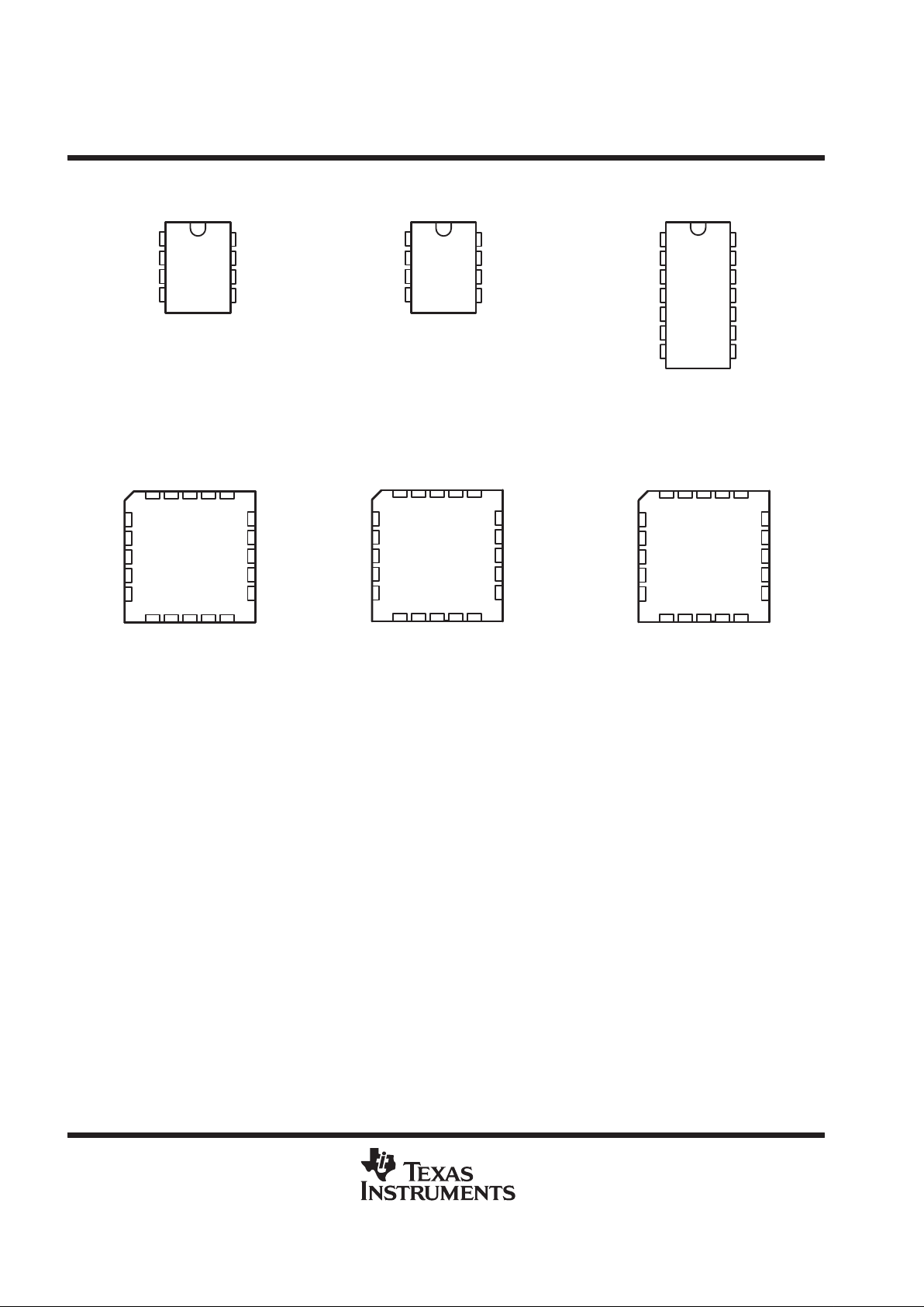
1
2
3
4
8
7
6
5
OFFSET N1
IN–
IN+
V
CC–
NC
V
CC+
OUT
OFFSET N2
3212019
910111213
4
5
6
7
8
18
17
16
15
14
NC
V
CC+
NC
OUT
NC
NC
IN–
NC
IN+
NC
NC
OFFSET N1
NC
NC
NC
NC
OFFSET N2
NC
NC
V
CC–
TL031x, TL031Ax
D, JG, OR P PACKAGE
(TOP VIEW)
1
2
3
4
8
7
6
5
1OUT
1IN–
1IN+
V
CC –
V
CC+
2OUT
2IN–
2IN+
3212019
910111213
4
5
6
7
8
18
17
16
15
14
NC
2OUT
NC
2IN–
NC
NC
1IN–
NC
1IN+
NC
NC
1OUT
NC
NC
NC
NC
2IN+
NC
CC–
V
CC+
V
TL031M, TL031AM
FK PACKAGE
(TOP VIEW)
TL032M, TL032AM
FK PACKAGE
(TOP VIEW)
TL032x, TL032Ax
D, JG, OR P PACKAGE
(TOP VIEW)
3212019
910111213
4
5
6
7
8
18
17
16
15
14
4IN+
NC
V
CC–
NC
3IN+
1IN+
NC
V
CC+
NC
2IN+
1IN–
1OUT
NC
3IN–
2IN–
NC
3OUT
4OUT
4IN–
2OUT
1
2
3
4
5
6
7
14
13
12
11
10
9
8
1OUT
1IN–
1IN+
V
CC+
2IN+
2IN–
2OUT
4OUT
4IN–
4IN+
V
CC–
3IN+
3IN–
3OUT
TL034x, TL034Ax
D, J, N, OR PW PACKAGE
(TOP VIEW)
TL034M, TL034AM
FK PACKAGE
(TOP VIEW)
NC – No internal connection
TL03x, TL03xA, TL03xY
ENHANCED-JFET LOW-POWER LOW-OFFSET
OPERATIONAL AMPLIFIERS
SLOS180B – FEBRUARY 1997 – REVISED FEBRUARY 1999
3
POST OFFICE BOX 655303 • DALLAS, TEXAS 75265
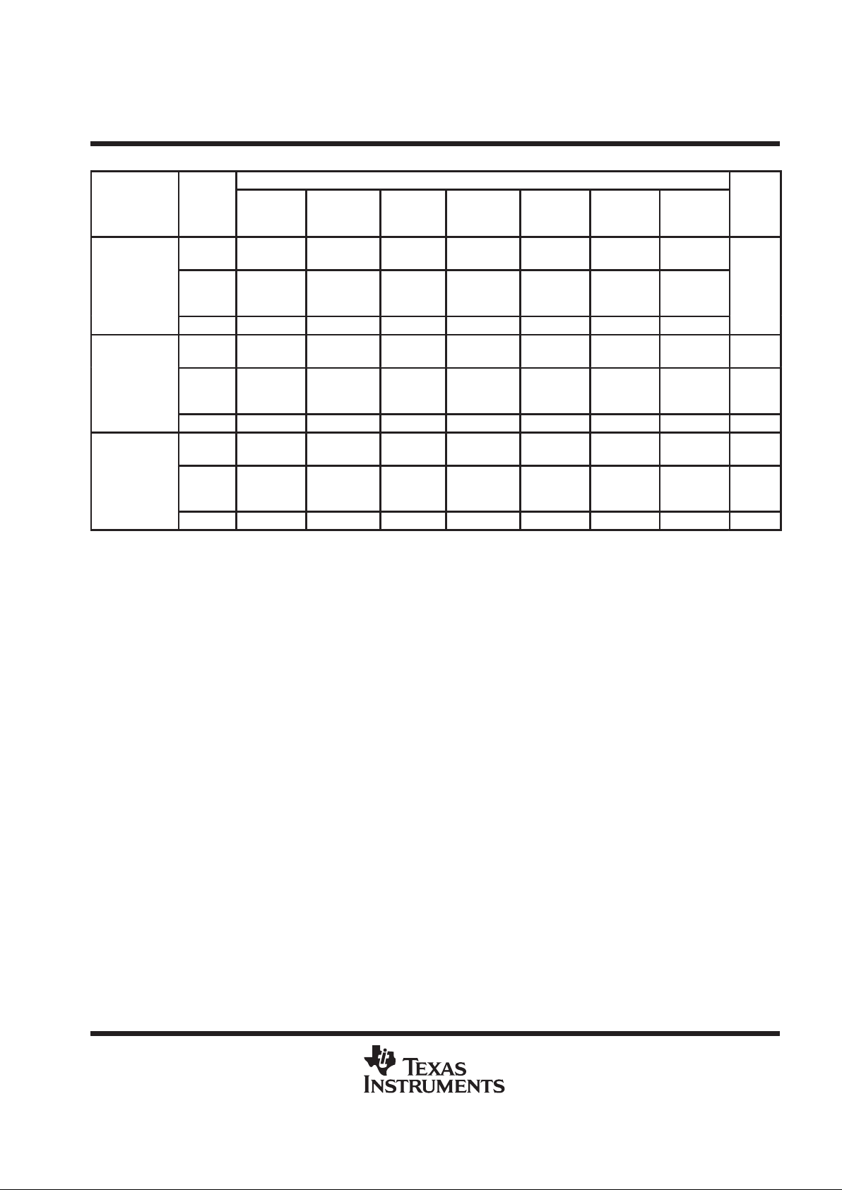
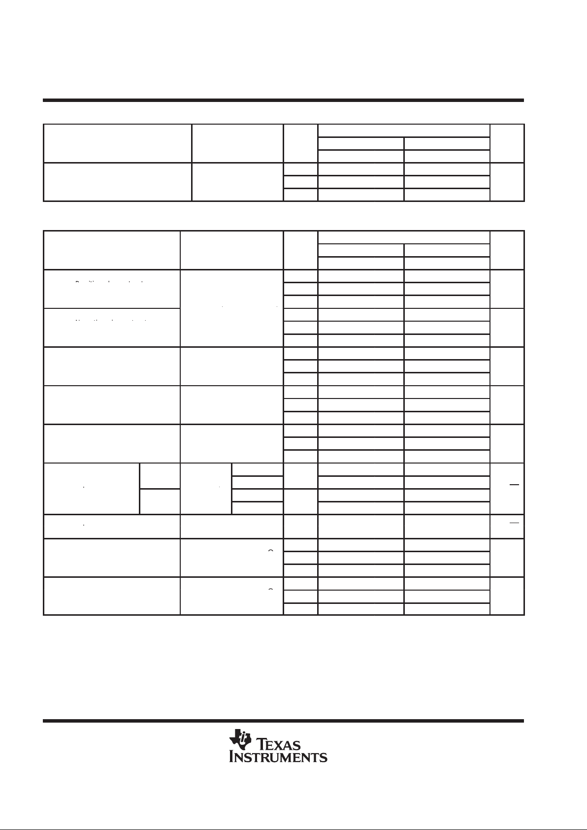
AVAILABLE OPTIONS
PACKAGED DEVICES
T
A
VIOMAX
AT 25°C
SMALL
OUTLINE
†
(D)
CHIP
CARRIER
(FK)
CERAMIC
DIP
(J)
CERAMIC
DIP
(JG)
PLASTIC
DIP
(N)
PLASTIC
DIP
(P)
TSSOP
†
(PW)
CHIP
FORM
‡
(Y)
0.8 mV
TL031ACD
TL032ACD
— — — —
TL031ACP
TL032ACP
—
0°C to 70°C
1.5 mV
TL031CD
TL032CD
TL034ACD
— — — TL034ACN
TL031CP
TL032CP
—
TL031Y
TL032Y
TL034Y
4 mV TL034CD — — — TL034CN TL034CPW
0.8 mV
TL031AID
TL032AID
— — — —
TL031AIP
TL032AIP
— —
–40°C to 85°C
1.5 mV
TL031ID
TL032ID
TL034AID
— — — TL034AIN
TL031IP
TL032IP
— —
4 mV TL034ID — — — TL034IN — — —
0.8 mV
TL031AMD
TL032AMD
TL031AMFK
TL032AMFK
—
TL031AMJG
TL032AMJG
—
TL031AMP
TL032AMP
— —
–55°C to 125°C
1.5 mV
TL031MD
TL032MD
TL034AMD
TL031MFK
TL032MFK
TL034AMFK
TL034AMJ
TL031MJG
TL032MJG
TL034AMN
TL031MP
TL032MP
— —
4 mV TL034MD TL034MFK TL034MJ — TL034MN — — —
†
The D and PW packages are available taped and reeled and are indicated by adding an R suffix to device type (e.g., TL034CDR or TL034CPWR).
‡
Chip forms are tested at 25°C.
TL03x, TL03xA, TL03xY
ENHANCED-JFET LOW-POWER LOW-OFFSET
OPERATIONAL AMPLIFIERS
SLOS180B – FEBRUARY 1997 – REVISED FEBRUARY 1999
4
POST OFFICE BOX 655303 • DALLAS, TEXAS 75265
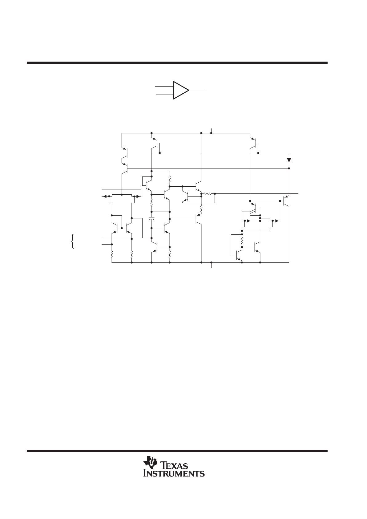
symbol (each amplifier)
–
+
OUT
IN–
IN+
equivalent schematic (each amplifier)
R2
OFFSET N2
OFFSET N1
IN–
IN+
Q2
Q3
Q5
V
CC+
Q14
Q6
R4
Q8
Q10
R7
Q11
R6
Q12
R3
C1
Q9
Q7
Q4
R5R1
Q1
JF1 JF2
Q13
Q16
R8
JF3 JF4
Q15
Q17
OUT
D1
V
CC–
NOTE A: OFFSET N1 and OFFSET N2 are available only on the TL031.
(see Note A)
TL03x, TL03xA, TL03xY
ENHANCED-JFET LOW-POWER LOW-OFFSET
OPERATIONAL AMPLIFIERS
SLOS180B – FEBRUARY 1997 – REVISED FEBRUARY 1999
5
POST OFFICE BOX 655303 • DALLAS, TEXAS 75265
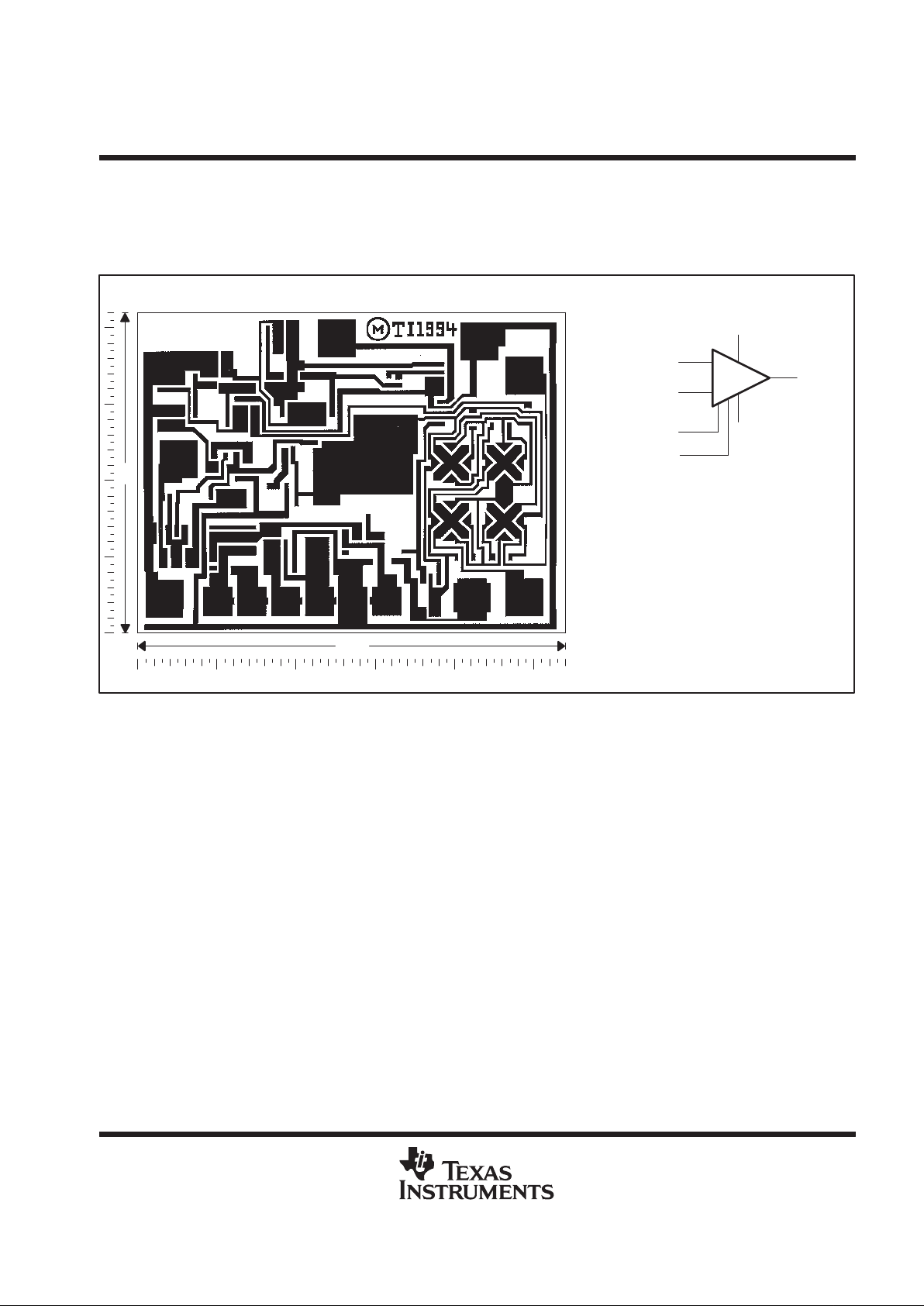
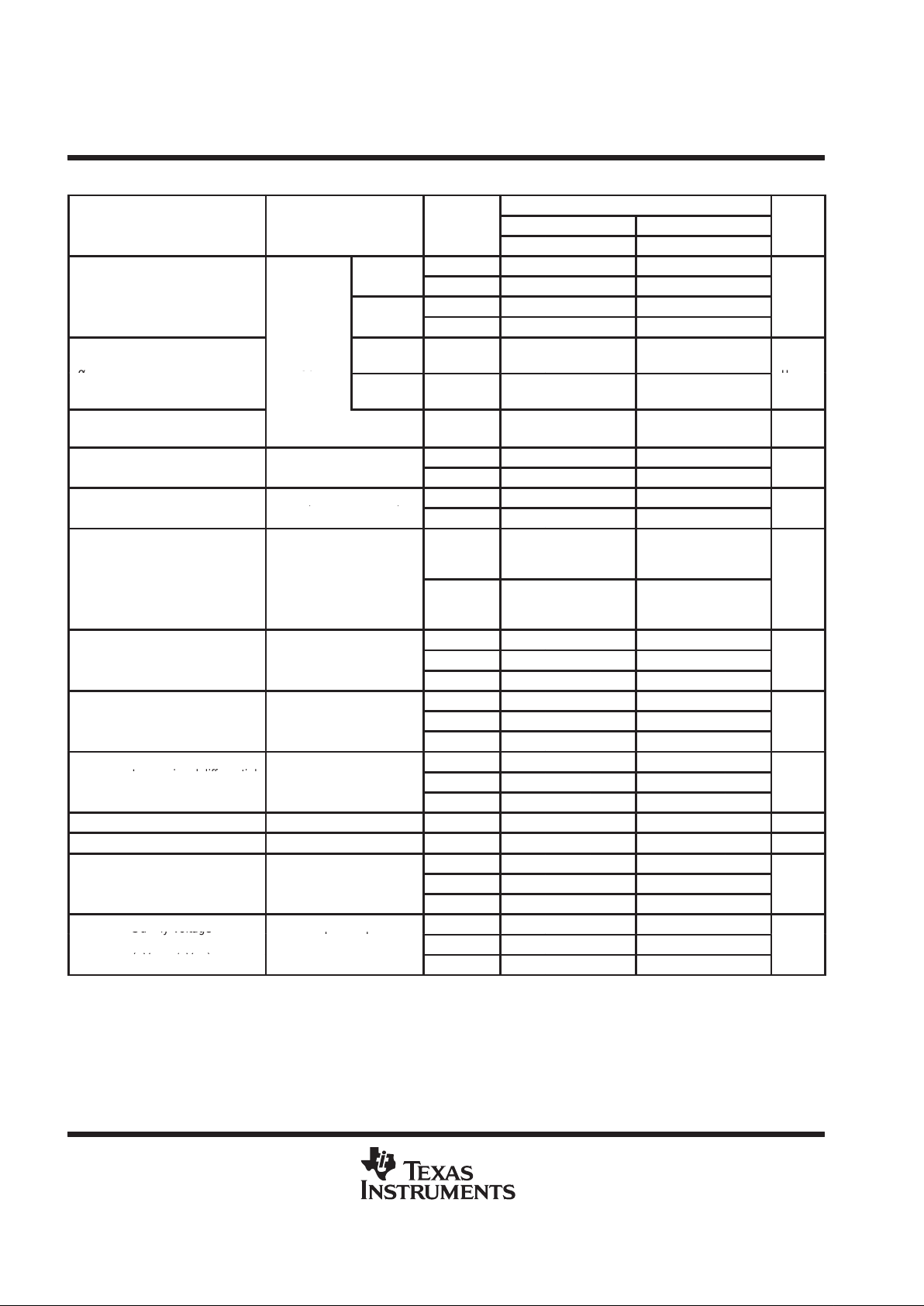
TL031Y chip information
This chip, when properly assembled, has characteristics similar to the TL031C. Thermal compression or
ultrasonic bonding can be used on the doped-aluminum bonding pads. These chips can be mounted with
conductive epoxy or a gold-silicon preform.
Bonding-Pad Assignments
54
42
Chip Thickness: 15 MIls Typical
Bonding Pads: 4 × 4 Mils Minimum
TJ(max) = 150°C
Tolerances Are ±10%.
All Dimensions Are in Mils.
Pin (4) is Internally Connected
to Backside of the Chip.
+
–
OUT
IN+
IN–
V
CC+
(7)
(3)
(2)
(6)
(1)
(4)
(5)
V
CC–
OFFSET N1
OFFSET N2
(1)
(2)
(3)
(4)
(6)
(7)
(8)
(5)
TL03x, TL03xA, TL03xY
ENHANCED-JFET LOW-POWER LOW-OFFSET
OPERATIONAL AMPLIFIERS
SLOS180B – FEBRUARY 1997 – REVISED FEBRUARY 1999
6
POST OFFICE BOX 655303 • DALLAS, TEXAS 75265
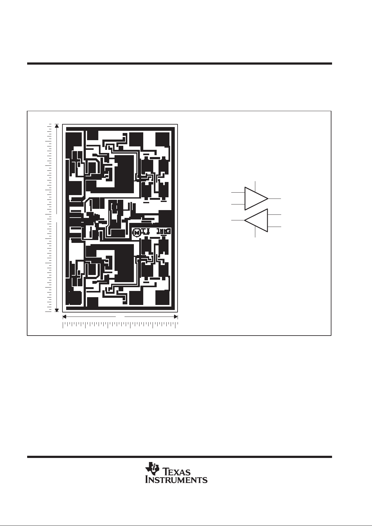
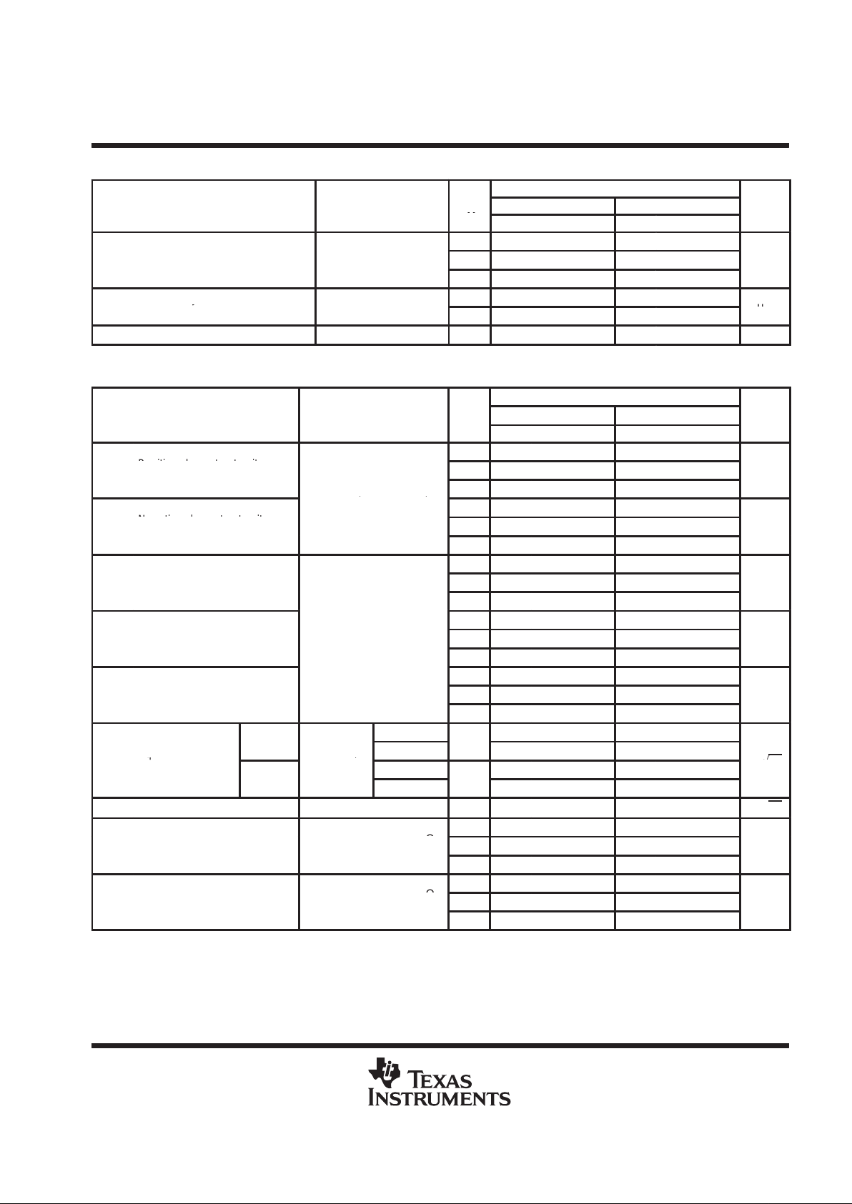
TL032Y chip information
This chip, when properly assembled, has characteristics similar to the TL032C. Thermal compression or
ultrasonic bonding can be used on the doped-aluminum bonding pads. These chips can be mounted with
conductive epoxy or a gold-silicon preform.
Bonding-Pad Assignments
Chip Thickness: 15 Mils Typical
Bonding Pads: 4 × 4 Mils Minimum
TJ(max) = 150°C
Tolerances Are ±10%.
All Dimensions Are in Mils.
Pin (4) is Internally Connected to Backside of Chip.
+
–
1OUT
1IN+
1IN–
V
CC+
(8)
(6)
(3)
(2)
(5)
(1)
–
+
(7)
2IN+
2IN–
2OUT
(4)
V
CC–
67
51
(6) (5)
(4)
(3)(2)(1)
(8)
(7)
TL03x, TL03xA, TL03xY
ENHANCED-JFET LOW-POWER LOW-OFFSET
OPERATIONAL AMPLIFIERS
SLOS180B – FEBRUARY 1997 – REVISED FEBRUARY 1999
7
POST OFFICE BOX 655303 • DALLAS, TEXAS 75265
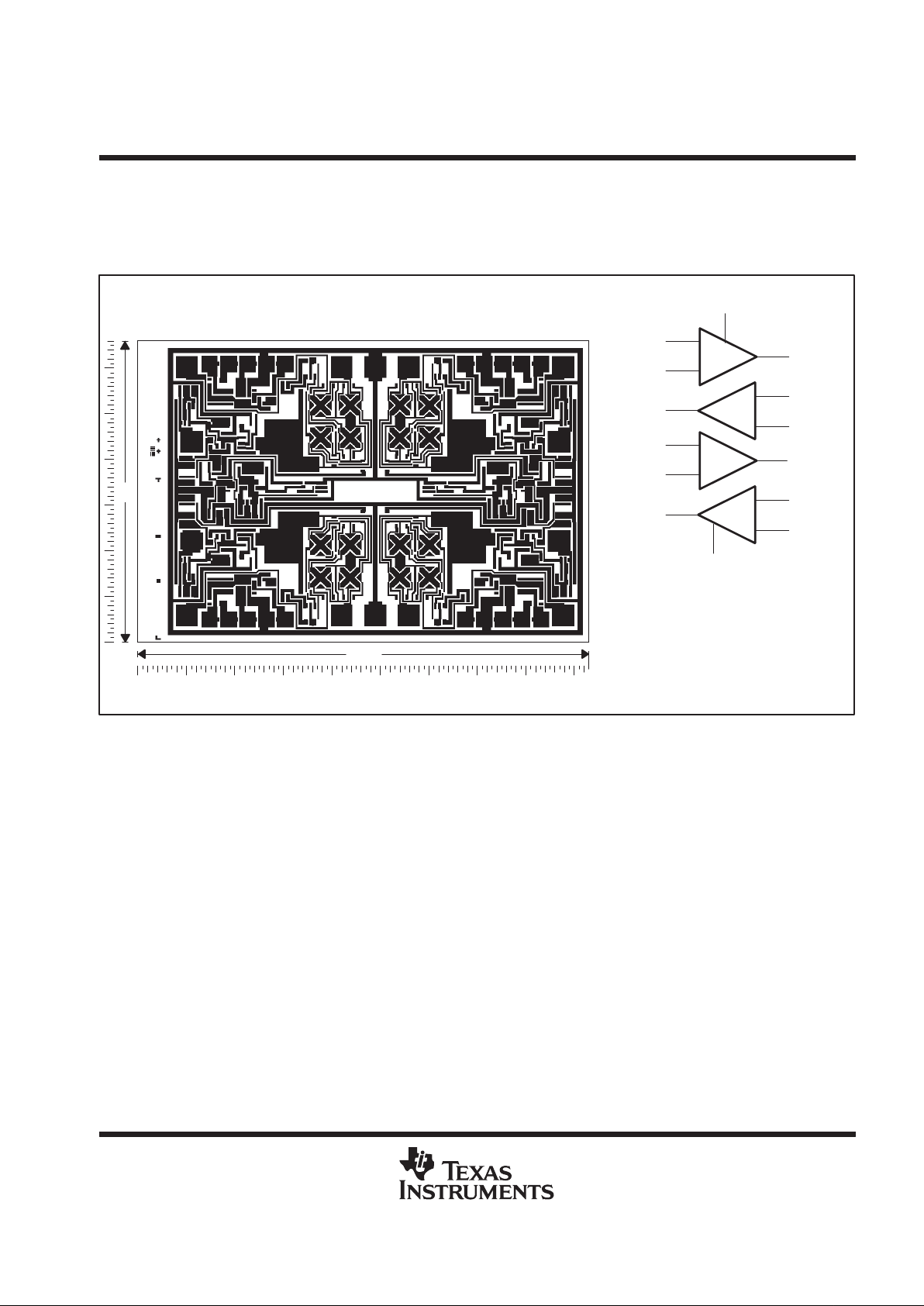
TL034Y chip information
This chip, when properly assembled, has characteristics similar to the TL034C. Thermal compression or
ultrasonic bonding can be used on the doped-aluminum bonding pads. These chips can be mounted with
conductive epoxy or a gold-silicon preform.
Bonding-Pad Assignments
+
–
1OUT
1IN+
1IN–
V
CC+
(4)
(6)
(3)
(2)
(5)
(1)
–
+
(7)
2IN+
2IN–
2OUT
(11)
V
CC–
+
–
3OUT
3IN+
3IN–
(13)
(10)
(9)
(12)
(8)
–
+
(14)
4OUT
4IN+
4IN–
(5)
(6)
(7)
(8)
(9)
(10)
93
66
(1)
(2) (3) (4) (5) (6)
(7)
(8)
(9)(10)(11)(12)(13)
(14)
Chip Thickness: 15 Mils Typical
Bonding Pads: 4 × 4 Mils Minimum
TJ(max) = 150°C
Tolerances Are ±10%.
All Dimensions Are in Mils.
Pin (11) is Internally Connected
to Backside of the Chip.
TL03x, TL03xA, TL03xY
ENHANCED-JFET LOW-POWER LOW-OFFSET
OPERATIONAL AMPLIFIERS
SLOS180B – FEBRUARY 1997 – REVISED FEBRUARY 1999
8
POST OFFICE BOX 655303 • DALLAS, TEXAS 75265
absolute maximum ratings over operating free-air temperature range (unless otherwise noted)
†
Supply voltage, V
CC+
(see Note 1) 18 V. . . . . . . . . . . . . . . . . . . . . . . . . . . . . . . . . . . . . . . . . . . . . . . . . . . . . . . . . .
Supply voltage, V
CC–
(see Note 1) –18 V. . . . . . . . . . . . . . . . . . . . . . . . . . . . . . . . . . . . . . . . . . . . . . . . . . . . . . . . .
Differential input voltage, V
ID
(see Note 2) ±30 V. . . . . . . . . . . . . . . . . . . . . . . . . . . . . . . . . . . . . . . . . . . . . . . . . .
Input voltage, VI (any input) (see Notes 1 and 3) ±15 V. . . . . . . . . . . . . . . . . . . . . . . . . . . . . . . . . . . . . . . . . . . . .
Input current, II (each input) ±1 mA. . . . . . . . . . . . . . . . . . . . . . . . . . . . . . . . . . . . . . . . . . . . . . . . . . . . . . . . . . . . . . .
Output current, IO (each output) ±40 mA. . . . . . . . . . . . . . . . . . . . . . . . . . . . . . . . . . . . . . . . . . . . . . . . . . . . . . . . . .
Total current into V
CC+
160 mA. . . . . . . . . . . . . . . . . . . . . . . . . . . . . . . . . . . . . . . . . . . . . . . . . . . . . . . . . . . . . . . . . .
Total current out of V
CC–
160 mA. . . . . . . . . . . . . . . . . . . . . . . . . . . . . . . . . . . . . . . . . . . . . . . . . . . . . . . . . . . . . . . .
Duration of short-circuit current at (or below) 25°C (see Note 4) Unlimited. . . . . . . . . . . . . . . . . . . . . . . . . . . . .
Continuous total power dissipation See Dissipation Rating Table. . . . . . . . . . . . . . . . . . . . . . . . . . . . . . . . . . . . .
Storage temperature range,T
stg
–65°C to 150°C. . . . . . . . . . . . . . . . . . . . . . . . . . . . . . . . . . . . . . . . . . . . . . . . . . .
Case temperature for 60 seconds: FK package 260°C. . . . . . . . . . . . . . . . . . . . . . . . . . . . . . . . . . . . . . . . . . . . . .
Lead temperature 1,6 mm (1 /16 inch) from case for 10 seconds: D, N, P, or PW package 260°C. . . . . . . . .
Lead temperature 1,6 mm (1 /16 inch) from case for 60 seconds: J or JG package 300°C. . . . . . . . . . . . . . .
†
Stresses beyond those listed under “absolute maximum ratings” may cause permanent damage to the device. These are stress ratings only, and
functional operation of the device at these or any other conditions beyond those indicated under “recommended operating conditions” is not
implied. Exposure to absolute-maximum-rated conditions for extended periods may affect device reliability.
NOTES: 1. All voltage values, except differential voltages, are with respect to the midpoint between V
CC+
and V
CC–
.
2. Differential voltages are at IN+ with respect to IN–.
3. The magnitude of the input voltage must never exceed the magnitude of the supply voltage or 15 V, whichever is less.
4. The output may be shorted to either supply. Temperature and/or supply voltages must be limited to ensure that the maximum
dissipation rating is not exceeded.
DISSIPATION RATING TABLE
PACKAGE
TA ≤ 25°C
POWER RATING
DERATING FACTOR
ABOVE TA = 25°C
TA = 70°C
POWER RATING
TA = 85°C
POWER RATING
TA = 125°C
POWER RATING
D 950 mW 7.6 mW/°C 608 mW 494 mW 190 mW
FK 1375 mW 11.0 mW/°C 880 mW 715 mW 275 mW
J 1375 mW 11.0 mW/°C 880 mW 715 mW 275 mW
JG 1050 mW 8.4 mW/°C 672 mW 546 mW 210 mW
N 1150 mW 9.2 mW/°C 736 mW 598 mW 230 mW
P 1100 mW 8.0 mW/°C 640 mW 520 mW 200 mW
PW 700 mW 5.6 mW/°C 448 mW N/A N/A
recommended operating conditions
C SUFFIX I SUFFIX M SUFFIX
MIN MAX MIN MAX MIN MAX
UNIT
Supply voltage, V
CC±
±5 ±15 ±5 ±15 ±5 ±15 V
p
V
CC±
= ±5 V –1.5 4 –1.5 4 –1.5 4
Common-mode input voltage, V
IC
V
CC±
= ±15 V –11.5 14 –11.5 14 –11.5 14
V
Operating free-air temperature, T
A
0 70 –40 85 –55 125 °C
TL03x, TL03xA, TL03xY
ENHANCED-JFET LOW-POWER LOW-OFFSET
OPERATIONAL AMPLIFIERS
SLOS180B – FEBRUARY 1997 – REVISED FEBRUARY 1999
9
POST OFFICE BOX 655303 • DALLAS, TEXAS 75265
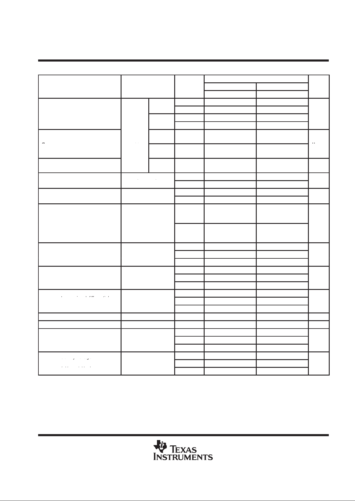
TL031C and TL031AC electrical characteristics at specified free-air temperature
TL031C, TL031AC
PARAMETER TEST CONDITIONS
T
A
V
CC±
= ±5 V V
CC±
= ±15 V
UNIT
A
MIN TYP MAX MIN TYP MAX
25°C 0.54 3.5 0.5 1.5
p
TL031C
Full range† 4.5 2.5
VIOInput offset voltage
25°C 0.41 2.8 0.34 0.8
mV
TL031AC
Full range† 3.8 1.8
V
O
= 0,
25°C to
T emperature coef ficient of
V
IC
= 0,
R
= 50 Ω
TL031C
70°C
7.1
5.9
°
α
VIO
input offset voltage
R
S
50
Ω
25°C to
µ
V/°C
TL031AC
70°C
7.1
5.9
25
Input offset voltage
long-term drift
‡
25°C 0.04 0.04 µV/mo
p
V
= 0, V
= 0,
25°C 1 100 1 100
p
IIOInput offset current
O
,
IC
,
See Figure 5
70°C 9 200 12 200
pA
p
V
= 0, V
= 0,
25°C 2 200 2 200
p
IIBInput bias current
O
,
IC
,
See Figure 5
70°C 50 400 80 400
pA
Common-mode input
25°C
–1.5
to
4
–3.4
to
5.4
–11.5
to
14
–13.4
to
15.4
V
ICR
voltage range
Full range
†
–1.5
to
.4
–11.5
to
14
V
25°C 3 4.3 13 14
V
OM+
Maximum positive peak
p
RL = 10 kΩ
0°C 3 4.2 13 14
V
out ut voltage swing
70°C 3 4.3 13 14
25°C –3 –4.2 –12.5 –13.9
V
OM–
Maximum negative peak
p
RL = 10 kΩ
0°C –3 –4.1 –12.5 –13.9
V
out ut voltage swing
70°C –3 –4.2 –12.5 –14
25°C 4 12 5 14.3
A
VD
Large-signal differential
p
§
RL = 10 kΩ
0°C 3 11.1 4 13.5
V/mV
voltage am lification
§
70°C 4 13.3 5 15.2
r
i
Input resistance 25°C 10
12
10
12
Ω
c
i
Input capacitance 25°C 5 4 pF
25°C 70 87 75 94
CMRR
Common-mode
VIC = V
ICR
min,
0°C 70 87 75 94
dB
rejection ratio
V
O
= 0,
R
S
= 50
Ω
70°C 70 87 75 94
Supply-voltage
25°C 75 96 75 96
k
SVR
Su ly voltage
rejection ratio
VO = 0, RS = 50 Ω
0°C 75 96 75 96
dB
(∆V
CC±
/∆VIO)
70°C 75 96 75 96
†
Full range is 0°C to 70°C.
‡
Typical values are based on the input offset voltage shift observed through 168 hours of operating life test at TA = 150°C extrapolated to
TA = 25°C using the Arrhenius equation and assuming an activation energy of 0.96 eV .
§
At V
CC±
= ±5 V, VO = ±2.3 V; at V
CC±
= ±15 V, VO = ±10 V .

TL03x, TL03xA, TL03xY
ENHANCED-JFET LOW-POWER LOW-OFFSET
OPERATIONAL AMPLIFIERS
SLOS180B – FEBRUARY 1997 – REVISED FEBRUARY 1999
10
POST OFFICE BOX 655303 • DALLAS, TEXAS 75265
TL031C and TL031AC electrical characteristics at specified free-air temperature (continued)
TL031C, TL031AC
PARAMETER TEST CONDITIONS
T
A
V
CC±
= ±5 V V
CC±
= ±15 V
UNIT
A
MIN TYP MAX MIN TYP MAX
25°C 1.9 2.5 6.5 8.4
P
D
Total power dissipation VO = 0, No load
0°C
1.8 2.5 6.3 8.4
mW
70°C 1.9 2.5 6.3 8.4
25°C 192 250 217 280
I
CC
Supply current VO = 0, No load
0°C
184 250 211 280
µA
70°C 189 250 210 280
TL031C and TL031AC operating characteristics at specified free-air temperature
TL031C, TL031AC
PARAMETER TEST CONDITIONS
T
A
V
CC±
= ±5 V V
CC±
= ±15 V
UNIT
A
MIN TYP MAX MIN TYP MAX
25°C 2 1.5 2.9
SR+
Positive slew rate at
†
0°C 1.8 1 2.6
V/µs
unity gain
†
R
= 10 kΩ, C
= 100 pF,
70°C
2.2 1.5 3.2
L
,
See Figure 1
L
,
25°C 3.9 1.5 5.1
SR–
Negative slew rate at
†
0°C 3.7 1.5 5
V/µs
unity gain
†
70°C 4 1.5 5
V
I(PP)
= ±10 mV , 25°C 138 132
t
r
Rise time
RL = 10 kΩ,
CL = 100 pF, 0°C 134 127
ns
See Figures 1 and 2 70°C 150 142
V
I(PP)
= ±10 mV , 25°C 138 132
t
f
Fall time
RL = 10 kΩ,
CL = 100 pF, 0°C 134 127
ns
See Figure 1 70°C 150 142
V
I(PP)
= ±10 mV , 25°C 11% 5%
Overshoot factor
CL = 100 pF,
CL = 100 pF, 0°C 10% 4%
See Figures 1 and 2 70°C 12% 6%
f = 10 Hz
°
61 61
Equivalent input
TL031C
R
= 20 Ω,
f = 1 kHz
25°C
41 41
V
n
q
noise voltage
S
,
See Figure 3
f = 10 Hz
°
61 61
n
V/√H
z
TL031AC
f = 1 kHz
25°C
41 41 60
I
n
Equivalent input noise
current
f = 1 kHz 25°C 0.003 0.003
pA/√Hz
25°C 1 1.1
B
1
Unity-gain bandwidth
VI = 10 mV,
p
RL = 10 kΩ,
0°C 1 1.1
MHz
C
L
= 25 F,
See Figure 4
70°C 1 1
25°C 61° 65°
φ
m
Phase margin at unity gain
V
I
= 10 mV,
=
p
R
L
= 10
kΩ
,
0°C 61° 65°
C
L
= 25 F,
See Figure 4
70°C 60° 64°
†
For V
CC±
= ±5 V, V
I(PP)
= ±1 V; for V
CC±
= ±15 V, V
I(PP)
= ±5 V.
TL03x, TL03xA, TL03xY
ENHANCED-JFET LOW-POWER LOW-OFFSET
OPERATIONAL AMPLIFIERS
SLOS180B – FEBRUARY 1997 – REVISED FEBRUARY 1999
11
POST OFFICE BOX 655303 • DALLAS, TEXAS 75265
TL031I and TL031AI electrical characteristics at specified free-air temperature
TL031I, TL031AI
PARAMETER TEST CONDITIONS
T
A
V
CC±
= ±5 V V
CC±
= ±15 V UNIT
A
MIN TYP MAX MIN TYP MAX
25°C 0.54 3.5 0.5 1.5
p
TL031I
Full range
†
5.3 3.3
VIOInput offset voltage
25°C 0.41 2.8 0.34 0.8
mV
TL031AI
Full range
†
4.6 2.6
VO = 0,
25°C to
T emperature coef ficient of
V
IC
= 0,
R
= 50 Ω
TL031I
85°C
6.5
6.2
°
α
VIO
input offset voltage
R
S
= 50
Ω
25°C to
µ
V/°C
TL031AI
85°C
6.5
6.2
25
Input offset voltage
°
g
long-term drift
‡
25°C
0.04
0.04µV/mo
p
VO = 0, VIC = 0, 25°C 1 100 1 100 pA
IIOInput offset current
See Figure 5 85°C 0.02 0.45 0.02 0.45 nA
p
VO = 0, VIC = 0, 25°C 2 200 2 200 pA
IIBInput bias current
See Figure 5 85°C 0.2 0.9 0.2 0.9 nA
Common-mode input
25°C
–1.5
to
4
–3.4
to
5.4
–11.5
to
14
–13.4
to
15.4
V
ICR
voltage range
Full range
†
–1.5
to
4
–11.5
to
14
V
25°C 3 4.3 13 14
V
OM+
Maximum positive peak
p
RL = 10 kΩ
–40°C 3 4.1 13 14
V
out ut voltage swing
85°C 3 4.4 13 14
25°C –3 –4.2 –12.5 –13.9
V
OM–
Maximum negative peak
p
RL = 10 kΩ
–40°C –3 –4.1 –12.5 –13.8
V
out ut voltage swing
85°C –3 –4.2 –12.5 –14
25°C 4 12 5 14.3
A
VD
Large-signal differential
p
§
RL = 10 kΩ
–40°C 3 8.4 4 11.6
V/mV
voltage am lification
§
85°C 4 13.5 5 15.3
r
i
Input resistance 25°C 10
12
10
12
Ω
c
i
Input capacitance 25°C 5 4 pF
25°C 70 87 75 94
CMRR
Common-mode
V
IC =
V
ICR
min
,
–40°C 70 87 75 94
dB
rejection ratio
VO = 0, RS = 50 Ω 85°C 70 87 75 94
pp
-
25°C 75 96 75 96
k
SVR
Su ly voltage
rejection ratio
VO = 0,
RS = 50 Ω
–40°C
75 96 75 96
dB
(∆V
CC±
/∆VIO)
85°C 75 96 75 96
†
Full range is –40°C to 85°C.
‡
Typical values are based on the input offset voltage shift observed through 168 hours of operating life test at TA = 150°C extrapolated to
TA = 25°C using the Arrhenius equation and assuming an activation energy of 0.96 eV .
§
At V
CC±
= ±5 V, VO = ±2.3 V; at V
CC±
= ±15 V, VO = ±10 V .
TL03x, TL03xA, TL03xY
ENHANCED-JFET LOW-POWER LOW-OFFSET
OPERATIONAL AMPLIFIERS
SLOS180B – FEBRUARY 1997 – REVISED FEBRUARY 1999
12
POST OFFICE BOX 655303 • DALLAS, TEXAS 75265
TL031I and TL031AI electrical characteristics at specified free-air temperature (continued)
TL031I, TL031AI
PARAMETER TEST CONDITIONS
T
A
V
CC±
= ±5 V V
CC±
= ±15 V UNIT
A
MIN TYP MAX MIN TYP MAX
25°C 1.9 2.5 6.5 8.4
P
D
Total power dissipation VO = 0, No load
–40°C
1.4 2.5 5.4 8.4
mW
85°C 1.9 2.5 6.2 8.4
25°C 192 250 217 280
I
CC
Supply current VO = 0, No load
–40°C
144 250 181 280
µA
85°C 189 250 207 280
TL031I and TL031AI operating characteristics at specified free-air temperature
TL031I, TL031AI
PARAMETER TEST CONDITIONS T
A
V
CC±
= ±5 V V
CC±
= ±15 V
UNIT
MIN TYP MAX MIN TYP MAX
25°C 2 1.5 2.9
SR+
Positive slew rate at
†
–40°C 1.6 1 2.1
V/µs
unity gain
†
R
= 10 kΩ C
= 100 pF,
85°C
2.3 1.5 3.3
L
See Figure 1
L
,
25°C 3.9 1.5 5.1
SR–
Negative slew rate at unity
†
–40°C 3.3 1.5 4.8
V/µs
gain
†
85°C 4.1 1.5 4.9
V
I(PP)
= ±10 mV , 25°C 138 132
t
r
Rise time
RL = 10 kΩ,
CL = 100 pF, –40°C 132 123
ns
See Figures 1 and 2 85°C 154 146
V
I(PP)
= ±10 mV , 25°C 138 132
t
f
Fall time
RL = 10 kΩ,
CL = 100 pF, –40°C 132 123
ns
See Figure 1 85°C 154 146
V
I(PP)
= ±10 mV , 25°C 11% 5%
Overshoot factor
RL = 10 kΩ,
CL = 100 pF, –40°C 12% 5%
See Figures 1 and 2 85°C 13% 7%
f = 10 Hz
°
61 61
Equivalent
TL031I
R
= 20 Ω,
f = 1 kHz
25°C
41 41
V
n
i
npu
t
S
,
See Figure 3
f = 10 Hz
°
61 61
n
V/√H
z
noise voltage
TL031AI
f = 1 kHz
25°C
41 41 60
Equivalent input noise
°
I
n
q
current
f
= 1 kHz
25°C
0.003
0.003
p
A/√H
z
25°C 1 1.1
B
1
Unity-gain bandwidth
VI = 10 mV
p
RL = 10 kΩ,
–40°C 1 1.1
MHz
C
L
= 25 F,
See Figure 4
85°C 0.9 1
25°C 61° 65°
φ
m
Phase margin at unity gain
V
I
= 10 mV,
=
p
R
L
= 10 kΩ,
–40°C 60° 65°
C
L
= 25
F
See Figure 4
85°C 60° 64°
†
For V
CC±
= ±5 V, V
I(PP)
= ±1 V; for V
CC±
= ±15 V, V
I(PP)
= ±5 V.
TL03x, TL03xA, TL03xY
ENHANCED-JFET LOW-POWER LOW-OFFSET
OPERATIONAL AMPLIFIERS
SLOS180B – FEBRUARY 1997 – REVISED FEBRUARY 1999
13
POST OFFICE BOX 655303 • DALLAS, TEXAS 75265
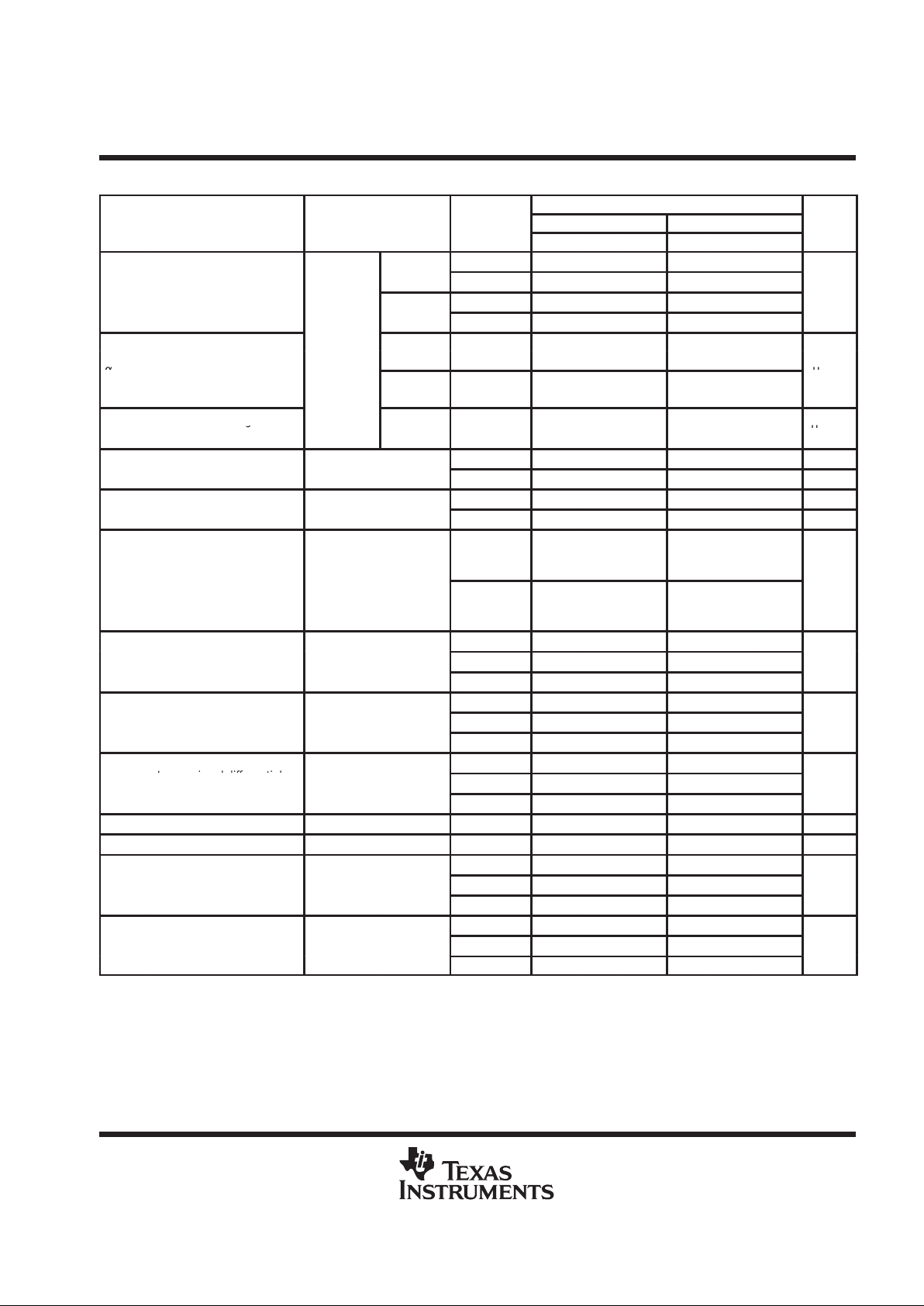
TL031M and TL031AM electrical characteristics at specified free-air temperature
TL031M, TL031AM
PARAMETER TEST CONDITIONS
T
A
V
CC±
= ±5 V V
CC±
= ±15 V
UNIT
A
MIN TYP MAX MIN TYP MAX
25°C 0.54 3.5 0.5 1.5
p
TL031M
Full range
†
6.5 4.5
VIOInput offset voltage
25°C 0.41 2.8 0.34 0.8
mV
TL031AM
Full range
†
5.8 3.8
T emperature coef ficient of
V
O
=
0
,
VIC = 0,
R
= 50 Ω
TL031M
25°C to
125°C
5.1 4.3
°
α
VIO
input offset voltage
R
S
50
Ω
TL031AM
25°C to
125°C
5.1 4.3
µ
V/°C
Input offset voltage
long-term drift
‡
25°C 0.04 0.04 µV/mo
p
VO = 0, VIC = 0, 25°C 1 100 1 100 pA
IIOInput offset current
See Figure 5 125°C 0.2 10 0.2 10 nA
p
VO = 0, VIC = 0, 25°C 2 200 2 200 pA
IIBInput bias current
See Figure 5 125°C 7 20 8 20 nA
Common-mode input
25°C
–1.5
to
4
–3.4
to
5.4
–11.5
to
14
–13.4
to
15.4
V
ICR
voltage range
Full range
†
–1.5
to
4
–11.5
to
14
V
25°C 3 4.3 13 14
V
OM+
Maximum positive peak
p
RL = 10 kΩ
–55°C 3 4.1 13 14
V
out ut voltage swing
125°C 3 4.4 13 14
25°C –3 –4.2 –12.5 –13.9
V
OM–
Maximum negative peak
p
RL = 10 kΩ
–55°C –3 –4 –12.5 –13.8
V
out ut voltage swing
125°C –3 –4.3 –12.5 –14
25°C 4 12 5 14.3
A
VD
Large-signal differential
p
§
RL = 10 kΩ
–55°C 3 7.1 4 10.4
V/mV
voltage am lification
§
125°C 3 12.9 4 15
r
i
Input resistance 25°C 10
12
10
12
Ω
c
i
Input capacitance 25°C 5 4 pF
25°C 70 87 75 94
CMR
Common-mode
VIC = V
ICR
min,
–55°C 70 87 70 94
dB
R
rejection ratio
V
O
= 0,
R
S
= 50
Ω
125°C 70 87 70 94
pp
-
25°C 75 96 75 96
k
SVR
Su ly voltage
rejection ratio
VO = 0,
RS = 50 Ω
–55°C
75 96 75 95
dB
(∆V
CC±
/∆VIO)
125°C 75 96 75 96
25°C 1.9 2.5 6.5 8.4
P
D
Total power dissipation VO = 0, No load
–55°C
1.1 2.5 4.7 8.4
mW
125°C 1.8 2.5 5.8 8.4
†
Full range is –55°C to 125°C.
‡
Typical values are based on the input offset voltage shift observed through 168 hours of operating life test at TA = 150°C extrapolated to
TA = 25°C using the Arrhenius equation and assuming an activation energy of 0.96 eV .
§
At V
CC±
= ±5 V, VO = ±2.3 V; at V
CC±
= ±15 V, VO = ±10 V .
TL03x, TL03xA, TL03xY
ENHANCED-JFET LOW-POWER LOW-OFFSET
OPERATIONAL AMPLIFIERS
SLOS180B – FEBRUARY 1997 – REVISED FEBRUARY 1999
14
POST OFFICE BOX 655303 • DALLAS, TEXAS 75265
TL031M and TL031AM electrical characteristics at specified free-air temperature (continued)
TL031M, TL031AM
PARAMETER TEST CONDITIONS
T
A
V
CC±
= ±5 V V
CC±
= ±15 V
UNIT
A
MIN TYP MAX MIN TYP MAX
25°C 192 250 217 280
I
CC
Supply current VO = 0, No load
–55°C
114 250 156 280
µA
125°C 178 250 197 280
TL031M and TL031AM operating characteristics at specified free-air temperature
TL031M, TL031AM
PARAMETER TEST CONDITIONS T
A
V
CC±
= ±5 V V
CC±
= ±15 V
UNIT
MIN TYP MAX MIN TYP MAX
25°C 2 1.5 2.9
SR+
Positive slew rate at
†
–55°C 1.4 1 1.9
V/µs
unity gain
†
R
= 10 kΩ, C
= 100 pF,
125°C
2.4 1 3.5
L
,
See Figure 1
L
,
25°C 3.9 1.5 5.1
SR–
Negative slew rate at
†
–55°C 3.2 1 4.6
V/µs
unity gain
†
125°C 4.1 1 4.7
V
I(PP)
= ±10 mV , 25°C 138 132
t
r
Rise time
RL = 10 kΩ,
CL = 100 pF, –55°C 142 123
ns
See Figures 1 and 2 125°C 166 158
V
I(PP)
= ±10 mV , 25°C 138 132
t
f
Fall time
RL = 10 kΩ,
CL = 100 pF, –55°C 142 123
ns
See Figure 1 125°C 166 158
V
I(PP)
= ±10 mV , 25°C 11% 5%
Overshoot factor
RL = 10 kΩ,
CL = 100 pF, –55°C 16% 6%
See Figures 1 and 2 125°C 14% 8%
f = 10 Hz
°
61 61
Equivalent input
TL031M
R
= 20 Ω,
f = 1 kHz
25°C
41 41
V
n
q
noise voltage
S
,
See Figure 3
f = 10 Hz
°
61 61
n
V/√H
z
TL031AM
f = 1 kHz
25°C
41 41
Equivalent input noise
°
I
n
q
current
f
= 1 kHz
25°C
0.003
0.003
p
A/√H
z
25°C 1 1.1
B
1
Unity-gain bandwidth
VI = 10 mV,
p
RL = 10 kΩ,
–55°C 1 1.1
MHz
C
L
= 25 F,
See Figure 4
125°C 0.9 0.9
25°C 61° 65°
φ
m
Phase margin at unity gain
VI = 10 mV,
p
RL = 10 kΩ,
–55°C 57° 64°
C
L
= 25 F,
See Figure 4
125°C 59° 62°
†
For V
CC±
= ±5 V, V
I(PP)
= ±1 V; for V
CC±
= ±15 V, V
I(PP)
= ±5 V.
TL03x, TL03xA, TL03xY
ENHANCED-JFET LOW-POWER LOW-OFFSET
OPERATIONAL AMPLIFIERS
SLOS180B – FEBRUARY 1997 – REVISED FEBRUARY 1999
15
POST OFFICE BOX 655303 • DALLAS, TEXAS 75265
TL031Y electrical characteristics, TA = 25°C
TL031Y
PARAMETER TEST CONDITIONS
V
CC±
= ±5 V V
CC±
= ±15 V
UNIT
MIN TYP MAX MIN TYP MAX
V
IO
Input offset voltage
0.54 0.5 mV
T emperature coef ficient of
V
O
= 0,
=
V
IC
= 0,
°
α
VIO
input offset voltage
R
S
= 50
Ω
7.1
5.9µV/°C
I
IO
Input offset current
V
= 0, V
= 0,
1 1 pA
I
IB
Input bias current
O
,
See Figure 5
IC
,
2 2 pA
V
ICR
Common-mode input voltage
range
–3.4
to
5.4
–13.4
to
15.4
V
V
OM+
Maximum positive peak
output voltage swing
RL = 10 kΩ 4.3 14 V
V
OM–
Maximum negative peak
output voltage swing
RL = 10 kΩ –4.2 –13.9 V
A
VD
Large-signal differential
voltage amplification
†
RL = 10 kΩ 12 14.3 V/mV
r
i
Input resistance 10
12
10
12
Ω
c
i
Input capacitance 5 4 pF
CMRR Common-mode rejection ratio
VIC = V
ICR
min,
RS = 50 Ω
VO = 0,
87 94 dB
k
SVR
Supply-voltage rejection ratio
(∆V
CC±
/∆VIO)
VO = 0, RS = 50 Ω 96 96 dB
P
D
Total power dissipation
1.9 6.5 mW
I
CC
Supply current
V
O
= 0,
No load
192 217 µA
†
At V
CC±
= ±5 V, VO = ±2.3 V; at V
CC±
= ±15 V, VO = ±10 V .
TL031Y operating characteristics, TA = 25°C
TL031Y
PARAMETER TEST CONDITIONS
V
CC±
= ±5 V V
CC±
= ±15 V
UNIT
MIN TYP MAX MIN TYP MAX
SR+
Positive slew rate at unity gain
‡
RL = 10 kΩ,pRL = 10 kΩ,
p
2 2.9 V/µs
SR–
Negative slew rate at unity gain
‡
C
L
=
100 pF
,
See Figure 1
C
L
=
100 pF
,
See Figure 1
3.9 5.1 V/µs
t
r
Rise time V
I(PP)
= ±10 mV , 138 132 ns
t
f
Fall time RL = 10 kΩ, CL = 100 pF, 138 132 ns
Overshoot factor See Figures 1 and 2 11% 5%
R
= 20 Ω,
f = 10 Hz 61 61
V
n
Equival
ent input noise voltage
S
,
See Figure 3
f = 1 kHz 41 41
n
V/√H
z
I
n
Equivalent input noise current f = 1 kHz 0.003 0.003
pA/√Hz
B
1
Unity-gain bandwidth
VI = 10 mV,
CL = 25 pF,
RL = 10 kΩ,
See Figure 4
1 1.1 MHz
φ
m
Phase margin at unity gain
VI = 10 mV,
CL = 25 pF,
RL = 10 kΩ,
See Figure 4
61° 65°
‡
For V
CC±
= ±5 V, V
I(PP)
= ±1 V; for V
CC±
= ±15 V, V
I(PP)
= ±5 V.
TL03x, TL03xA, TL03xY
ENHANCED-JFET LOW-POWER LOW-OFFSET
OPERATIONAL AMPLIFIERS
SLOS180B – FEBRUARY 1997 – REVISED FEBRUARY 1999
16
POST OFFICE BOX 655303 • DALLAS, TEXAS 75265
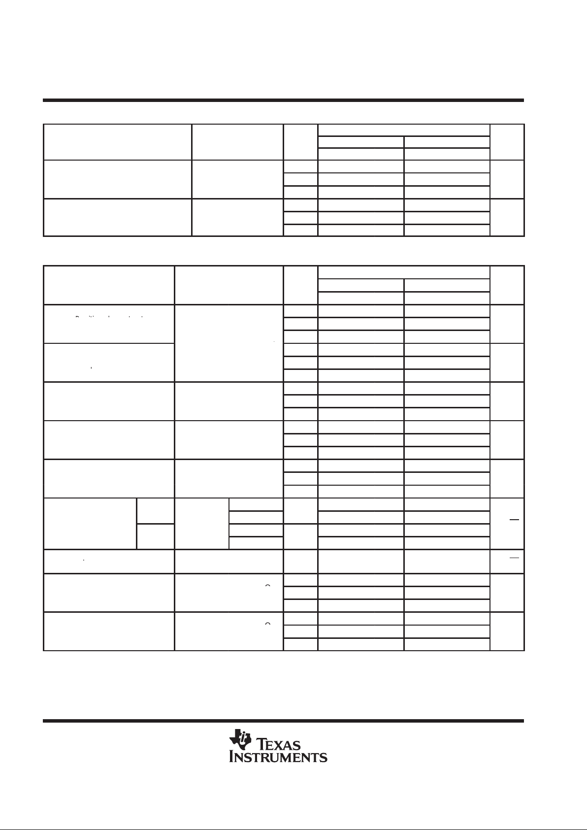
TL032C and TL032AC electrical characteristics at specified free-air temperature
TL032C, TL032AC
PARAMETER TEST CONDITIONS
T
A
V
CC±
= ±5 V V
CC±
= ±15 V
UNIT
A
MIN TYP MAX MIN TYP MAX
25°C 0.69 3.5 0.57 1.5
p
TL032C
Full range
†
4.5 2.5
VIOInput offset voltage
25°C 0.53 2.8 0.39 0.8
mV
TL032AC
Full range
†
3.8 1.8
T emperature coef ficient
V
O
=
0
,
VIC = 0,
R
= 50 Ω
TL032C
25°C to
70°C
11.5 10.8
°
α
VIO
of input offset voltage
R
S
50
Ω
TL032AC
25°C to
70°C
11.5 10.8 25
µ
V/°C
Input offset voltage
long-term drift
‡
25°C 0.04 0.04 µV/mo
p
V
= 0, V
= 0,
25°C 1 100 1 100
p
IIOInput offset current
O
,
See Figure 5
IC
,
70°C 9 200 12 200
pA
p
V
= 0, V
= 0,
25°C 2 200 2 200
p
IIBInput bias current
O
,
See Figure 5
IC
,
70°C 50 400 80 400
pA
Common-mode input
25°C
–1.5
to
4
–3.4
to
5.4
–11.5
to
14
–13.4
to
15.4
V
ICR
voltage range
Full range
†
–1.5
to
4
–11.5
to
14
V
25°C 3 4.3 13 14
V
OM+
Maximum positive peak
p
RL = 10 kΩ
0°C 3 4.2 13 14
V
out ut voltage swing
70°C 3 4.3 13 14
25°C –3 –4.2 –12.5 –13.9
V
OM–
Maximum negative
peak output voltage
RL = 10 kΩ
0°C –3 –4.1 –12.5 –13.9
V
swing
70°C –3 –4.2 –12.5 –14
25°C 4 12 5 14.3
A
VD
Large-signal differential
p
§
RL = 10 kΩ
0°C 3 11.1 4 13.5
V/mV
voltage am lification
§
70°C 4 13.3 5 15.2
r
i
Input resistance 25°C 10
12
10
12
Ω
c
i
Input capacitance 25°C 5 14 pF
25°C 70 87 75 94
CMRR
Common-mode
VIC = V
ICR
min,
0°C 70 87 75 94
dB
rejection ratio
V
O
= 0,
R
S
= 50
Ω
70°C 70 87 75 94
Supply-voltage
25°C 75 96 75 96
k
SVR
Su ly voltage
rejection ratio
V
CC±
= ±
5 V t
o ±15 V,
=
=
0°C 75 96 75 96
dB
(∆V
CC±
/∆VIO)
V
O
= 0,
R
S
= 50
Ω
70°C 75 96 75 96
†
Full range is 0°C to 70°C.
‡
Typical values are based on the input offset voltage shift observed through 168 hours of operating life test at TA = 150°C extrapolated to
TA = 25°C using the Arrhenius equation and assuming an activation energy of 0.96 eV .
§
At V
CC±
= ±5 V, VO = 2.3 V; at V
CC±
= ±15 V, VO = ±10 V .
TL03x, TL03xA, TL03xY
ENHANCED-JFET LOW-POWER LOW-OFFSET
OPERATIONAL AMPLIFIERS
SLOS180B – FEBRUARY 1997 – REVISED FEBRUARY 1999
17
POST OFFICE BOX 655303 • DALLAS, TEXAS 75265
TL032C and TL032AC electrical characteristics at specified free-air temperature (continued)
TL032C, TL032AC
PARAMETER TEST CONDITIONS
T
A
V
CC±
= ±5 V V
CC±
= ±15 V UNIT
A
MIN TYP MAX MIN TYP MAX
25°C 3.8 5 13 17
P
D
Total power dissipation
p
VO = 0, No load
0°C
3.7 5 12.7 17
mW
(two am lifiers)
70°C 3.8 5 12.6 17
Supply current
0°C 368 500 422 560
I
CC
y
(two amplifiers)
V
O
= 0,
No load
70°C 378 500 420 560
µ
A
VO1/V
O2
Crosstalk attenuation AVD = 100 dB 25°C 120 120 dB
TL032C and TL032AC operating characteristics at specified free-air temperature
TL032C, TL032AC
PARAMETER TEST CONDITIONS T
A
V
CC±
= ±5 V V
CC
±
= ±15 V
UNIT
MIN TYP MAX MIN TYP MAX
25°C 12 1.5 2.9
SR+
Positive slew rate at unity
†
0°C 1.8 1 2.6
V/µs
gain
†
R
= 10 kΩ, C
= 100 pF,
70°C 2.2 1.5 3.2
L
,
L
,
See Figure 1
25°C 3.9 1.5 5.1
SR–
Negative slew rate at unity
†
0°C 3.7 1.5 5
V/µs
gain
†
70°C 4 1.5 5
25°C 138 132
t
r
Rise time
0°C 134 127
ns
70°C 150 142
=
25°C 138 132
t
f
Fall time
V
I(PP)
=
±10 V
,
RL = 10 kΩ, CL = 100 pF,
0°C 134 127
ns
See Figures 1 and 2
70°C 150 142
25°C 11% 5%
Overshoot factor
0°C 10% 4%
70°C 12% 6%
f = 10 Hz
°
49 49
Equivalent input
TL032C
R
= 20 Ω,
f = 1 kHz
25°C
41 41
V
n
q
noise voltage
S
,
See Figure 3
f = 10 Hz
°
49 49
n
V/√H
z
TL032AC
f = 1 kHz
25°C
41 41 60
I
n
Equivalent input noise current f = 1 kHz 25°C 0.003 0.003
pA/√Hz
25°C 1 1.1
B
1
Unity-gain bandwidth
VI = 10 mV,
p
RL = 10 kΩ,
0°C 1 1.1
MHz
C
L
= 25 F,
See Figure 4
70°C 1 1
25°C 61° 65°
φ
m
Phase margin at unity gain
V
I
= 10 mV,
=
p
R
L
= 10 kΩ,
0°C 61° 65°
C
L
= 25 F,
See Figure 4
70°C 60° 64°
†
For V
CC±
= ±5 V, V
I(PP)
= ±1 V; for V
CC±
= ±15 V, V
I(PP)
= ±5 V.

TL03x, TL03xA, TL03xY
ENHANCED-JFET LOW-POWER LOW-OFFSET
OPERATIONAL AMPLIFIERS
SLOS180B – FEBRUARY 1997 – REVISED FEBRUARY 1999
18
POST OFFICE BOX 655303 • DALLAS, TEXAS 75265
TL032I and TL032AI electrical characteristics at specified free-air temperature
TL032I, TL032AI
PARAMETER TEST CONDITIONS
T
A
V
CC±
= ±5 V V
CC±
= ±15 V UNIT
A
MIN TYP MAX MIN TYP MAX
25°C 0.69 3.5 0.57 1.5
p
TL032I
Full range
†
5.3 3.3
VIOInput offset voltage
25°C 0.53 2.8 0.39 0.8
mV
TL032AI
Full range
†
4.6 2.6
T emperature coef ficient
V
O
= 0,
VIC = 0,
R
= 50 Ω
TL032I
25°C to
85°C
11.4 10.8
°
α
VIO
of input offset voltage
R
S
50
Ω
TL032AI
25°C to
85°C
11.4 10.8 25
µ
V/°C
Input offset voltage
long-term drift
‡
25°C 0.04 0.04 µV/mo
p
V
= 0, V
= 0,
25°C 1 100 1 100 pA
IIOInput offset current
O
,
See Figure 5
IC
,
85°C 0.02 0.45 0.02 0.45 nA
p
V
= 0, V
= 0,
25°C 2 200 2 200 pA
IIBInput bias current
O
,
See Figure 5
IC
,
85°C 0.2 0.9 0.3 0.9 nA
Common-mode input
25°C
–1.5
to
4
–3.4
to
5.4
–11.5
to
14
–13.4
to
15.4
V
ICR
voltage range
Full range
†
–1.5
to
4
–11.5
to
14
V
25°C 3 4.3 13 14
V
OM+
Maximum positive peak
p
RL = 10 kΩ
–40°C 3 4.2 13 14
V
out ut voltage swing
85°C 3 4.4 13 14
25°C –3 –4.2 –12.5 –13.9
V
OM–
Maximum negative
peak output voltage
RL = 10 kΩ
–40°C –3 –4.1 –12.5 –13.8
V
swing
85°C –3 –4.2 –12.5 –14
Large-signal differential
–40°C 3 8.4 4 11.6
A
VD
gg
voltage amplification
§
R
L
= 10
kΩ
85°C 4 13.5 5 15.3
V/mV
r
i
Input resistance 25°C 10
12
10
12
Ω
c
i
Input capacitance 25°C 5 4 pF
25°C 70 87 75 94
CMRR
Common-mode
VIC = V
ICR
min,
–40°C 70 87 75 94
dB
rejection ratio
V
O
= 0,
R
S
= 50
Ω
85°C 70 87 75 94
Supply-voltage
25°C 75 96 75 96
k
SVR
Su ly voltage
rejection ratio
V
CC±
= ±5 V to
±15 V
,
–40°C 75 96 75 96
dB
(∆V
CC±
/∆VIO)
VO = 0, RS = 50 Ω 85°C 75 96 75 96
†
Full range is –40°C to 85°C.
‡
Typical values are based on the input offset voltage shift observed through 168 hours of operating life test at TA = 150°C extrapolated to
TA = 25°C using the Arrhenius equation and assuming an activation energy of 0.96 eV .
§
At V
CC±
= ±5 V, VO = 2.3 V; at V
CC±
= ±15 V, VO = ±10 V .

TL03x, TL03xA, TL03xY
ENHANCED-JFET LOW-POWER LOW-OFFSET
OPERATIONAL AMPLIFIERS
SLOS180B – FEBRUARY 1997 – REVISED FEBRUARY 1999
19
POST OFFICE BOX 655303 • DALLAS, TEXAS 75265
TL032I and TL032AI electrical characteristics at specified free-air temperature (continued)
TL032I, TL032AI
PARAMETER TEST CONDITIONS
T
A
V
CC±
= ±5 V V
CC±
= ±15 V UNIT
A
MIN TYP MAX MIN TYP MAX
25°C 3.8 5 13 17
P
D
Total power dissipation
p
VO = 0, No load
–40°C 2.9 5 10.9 17
mW
(two am lifiers)
85°C 3.7 5 12.4 17
25°C 384 500 434 560
I
CC
Supply current
p
VO = 0, No load
–40°C 288 500 362 560
µA
(two am lifiers)
85°C 372 500 414 560
VO1/V
O2
Crosstalk attenuation AVD = 100 dB 25°C 120 120 dB
TL032I and TL032AI operating characteristics at specified free-air temperature
TL032I, TL032AI
PARAMETER TEST CONDITIONS T
A
V
CC±
= ±5 V V
CC±
= ±15 V UNIT
MIN TYP MAX MIN TYP MAX
25°C 2 1.5 2.9
SR+
Positive slew rate at unity
†
–40°C 1.6 1 2.1
V/µs
gain
†
p
85°C 2.3 1.5 3.3
R
L
=
10 kΩ, C
L
=
100 pF
25°C 3.9 1.5 5.1
SR–
Negative slew rate at unity
†
–40°C 3.3 1.5 4.8
V/µs
gain
†
85°C 4.1 1.5 4.9
=
25°C 138 132
t
r
Rise time
V
I(PP)
=
±10 V
,
RL = 10 kΩ, CL = 100 pF,
–40°C 132 123
ns
See Figures 1 and 2
85°C 154 146
=
25°C 138 132
t
f
Fall time
V
I(PP)
=
±10 V
,
RL = 10 kΩ, CL = 100 pF,
–40°C 132 123
ns
See Figure 1
85°C 154 146
=
25°C 11% 5%
Overshoot factor
V
I(PP)
=
±10 V
,
RL = 10 kΩ, CL = 100 pF,
–40°C 12% 5%
See Figures 1 and 2
85°C 13% 7%
f = 10 Hz
°
49 49
Equivalent input
TL032I
R
= 20 Ω,
f = 1 kHz
25°C
41 41
V
n
q
noise voltage
S
,
See Figure 3
f = 10 Hz
°
49 49
n
V/√H
z
TL032AI
f = 1 kHz
25°C
41 41 60
I
n
Equivalent input noise
current
f = 1 kHz 25°C 0.003 0.003
pA/√Hz
25°C 1 1.1
B1Unity-gain bandwidth
VI = 10 mV,
p
RL = 10 kΩ,
–40°C 1 1.1
MHz
C
L
= 25 F,
See Figure 4
85°C 0.9 1
25°C 61° 65°
φmPhase margin at unity gain
V
I
= 10 mV,
=
p
R
L
= 10 kΩ,
–40°C 61° 65°
C
L
= 25 F,
See Figure 4
85°C 60° 64°
†
For V
CC±
= ±5 V, V
I(PP)
= ±1 V; for V
CC±
= ±15 V, V
I(PP)
= ±5 V.

TL03x, TL03xA, TL03xY
ENHANCED-JFET LOW-POWER LOW-OFFSET
OPERATIONAL AMPLIFIERS
SLOS180B – FEBRUARY 1997 – REVISED FEBRUARY 1999
20
POST OFFICE BOX 655303 • DALLAS, TEXAS 75265
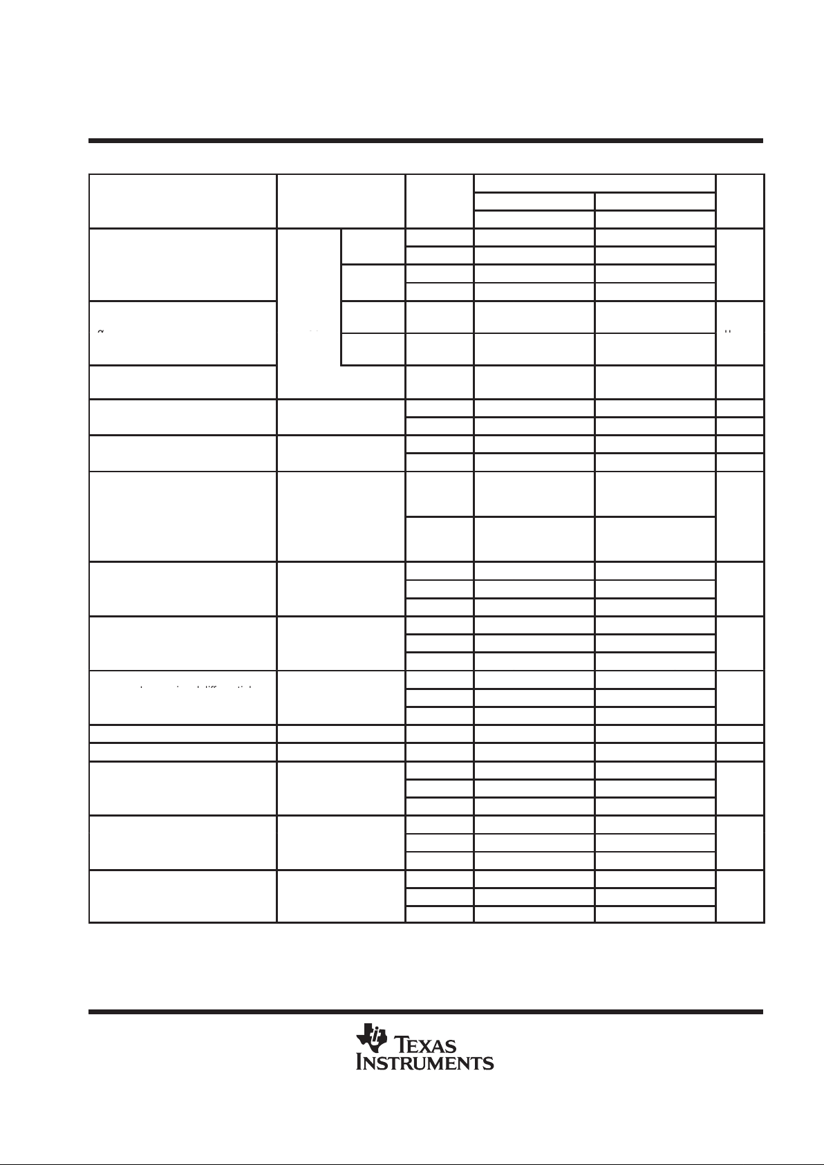
TL032M and TL032AM electrical characteristics at specified free-air temperature
TL032M, TL032AM
PARAMETER TEST CONDITIONS
T
A
V
CC±
= ±5 V V
CC±
= ±15 V UNIT
A
MIN TYP MAX MIN TYP MAX
25°C 0.69 3.5 0.57 1.5
p
TL032M
Full range
†
6.5 4.5
VIOInput offset voltage
25°C 0.53 2.8 0.39 0.8
mV
TL032AM
Full range
†
5.8 3.8
T emperature coef ficient
V
O
= 0,
VIC = 0,
R
= 50 Ω
TL032M
25°C to
125°C
9.7 9.7
°
α
VIO
of input offset voltage
R
S
50
Ω
TL032AM
25°C to
125°C
9.7 9.7
µ
V/°C
Input offset voltage
long-term drift
‡
25°C 0.04 0.04 µV/mo
p
V
= 0, V
= 0,
25°C 1 100 1 100 pA
IIOInput offset current
O
,
See Figure 5
IC
,
125°C 0.2 10 0.2 10 nA
p
V
= 0, V
= 0,
25°C 2 200 2 200 pA
IIBInput bias current
O
,
See Figure 5
IC
,
125°C 7 20 8 20 nA
Common-mode input
25°C
–1.5
to
4
–3.4
to
5.4
–11.5
to
14
–13.4
to
15.4
V
ICR
voltage range
Full range
†
–1.5
to
4
–11.5
to
14
V
25°C 3 4.3 13 14
V
OM+
Maximum positive peak
p
RL = 10 kΩ
–55°C 3 4.1 13 14
V
out ut voltage swing
125°C 3 4.4 13 14
25°C –3 –4.2 –12.5 –13.9
V
OM–
Maximum negative peak
p
RL = 10 kΩ
–55°C –3 –4 –12.5 –13.8
V
out ut voltage swing
125°C –3 –4.3 –12.5 –14
25°C 4 12 5 14.3
A
VD
Large-signal differential
p
§
RL = 10 kΩ
–55°C 3 7.1 4 10.4
V/mV
voltage am lification
§
125°C 3 12.9 4 15
r
i
Input resistance 25°C 10
12
10
12
Ω
c
i
Input capacitance 25°C 5 4 pF
25°C 70 87 75 94
CMRR
Common-mode rejection
VIC = V
ICR
min,
–55°C 70 87 70 94
dB
ratio
V
O
= 0,
R
S
= 50
Ω
125°C 70 87 70 94
Supply-voltage
25°C 75 96 75 96
k
SVR
Su ly voltage
rejection ratio
V
CC±
= ±5 V to ±15 V,
=
=
–55°C 75 95 75 95
dB
(∆V
CC±
/∆VIO)
V
O
= 0,
R
S
= 50
Ω
125°C 75 96 75 96
†
Full range is –55°C to 125°C.
‡
Typical values are based on the input offset voltage shift observed through 168 hours of operating life test at TA = 150°C extrapolated to
TA = 25°C using the Arrhenius equation and assuming an activation energy of 0.96 eV .
§
At V
CC±
= ±5 V, VO = 2.3 V; at V
CC±
= ±15 V, VO = ±10 V .

TL03x, TL03xA, TL03xY
ENHANCED-JFET LOW-POWER LOW-OFFSET
OPERATIONAL AMPLIFIERS
SLOS180B – FEBRUARY 1997 – REVISED FEBRUARY 1999
21
POST OFFICE BOX 655303 • DALLAS, TEXAS 75265
TL032M and TL032AM electrical characteristics at specified free-air temperature (continued)
TL032M, TL032AM
PARAMETER TEST CONDITIONS
T
A
V
CC±
= ±5 V V
CC±
= ±15 V UNIT
A
MIN TYP MAX MIN TYP MAX
25°C 3.8 5 13 17
P
D
Total power dissipation
p
VO = 0, No load
–55°C
2.3 5 9.4 17
mW
(two am lifiers)
125°C 3.6 5 11.8 17
25°C 384 500 434 560
I
CC
Supply current
p
VO = 0, No load
–55°C
228 500 312 560
µA
(two am lifiers)
125°C 356 500 394 560
VO1/V
O2
Crosstalk attenuation AVD = 100 dB 25°C 120 120 dB
TL032M and TL032AM operating characteristics at specified free-air temperature
TL032M, TL032AM
PARAMETER TEST CONDITIONS T
A
V
CC±
= ±5 V V
CC±
= ±15 V UNIT
MIN TYP MAX MIN TYP MAX
25°C 2 1.5 2.9
SR+
Positive slew rate at unity
†
–55°C 1.4 1 1.9
V/µs
gain
†
RL = 10 kΩ,
p
125°C 2.4 1 3.5
C
L
=
100 pF
,
See and
Figure 1
25°C 3.9 1.5 5.1
SR–
Negative slew rate at unity
†
See and Figure 1
–55°C 3.2 1 4.6
V/µs
gain
†
125°C 4.1 1 4.7
V
I(PP)
= ±10 V ,
25°C 138 132
t
r
Rise time
()
RL = 10 kΩ,
=
p
–55°C 142 123
ns
C
L
=
100 F
,
See Figures 1 and 2
125°C 166 58
V
I(PP)
= ±10 V ,
25°C 138 132
t
f
Fall time
()
RL = 10 kΩ,
=
p
–55°C 142 123
ns
C
L
=
100 F
,
See Figure 1
125°C 166 158
V
I(PP)
= ±10 V ,
25°C 11% 5%
Overshoot factor
()
RL = 10 kΩ,
=
p
–55°C 16% 6%
C
L
=
100 F
,
See Figures 1 and 2
125°C 14% 8%
f = 10 Hz
°
49 49
Equivalent
p
TL032M
R
= 20 Ω,
f = 1 kHz
25°C
41 41
V
n
i
nput noise
volt
age
S
,
See Figure 3
f = 10 Hz
°
49 49
n
V/√H
z
voltage
TL032AM
f = 1 kHz
25°C
41 41
I
n
Equivalent input noise
current
f = 1 kHz 25°C 0.003 0.003
pA/√Hz
25°C 1 1.1
B1 Unity-gain bandwidth
VI = 10 mV,
p
RL = 10 kΩ,
–55°C 1 1.1
MHz
C
L
= 25 F,
See Figure 4
125°C 0.9 0.9
25°C 61° 65°
φ
m
Phase margin at unity gain
V
I
= 10 mV,
=
p
R
L
= 10 kΩ,
–55°C 57° 64°
C
L
= 25 F,
See Figure 4
125°C 59° 62°
†
For V
CC±
= ±5 V, V
I(PP)
= ±1 V; for V
CC±
= ±15 V, V
I(PP)
= ±5 V.

TL03x, TL03xA, TL03xY
ENHANCED-JFET LOW-POWER LOW-OFFSET
OPERATIONAL AMPLIFIERS
SLOS180B – FEBRUARY 1997 – REVISED FEBRUARY 1999
22
POST OFFICE BOX 655303 • DALLAS, TEXAS 75265
TL032Y electrical characteristics, TA = 25°C
TL032Y
PARAMETER TEST CONDITIONS V
CC±
= ±5 V V
CC±
= ±15 V UNIT
MIN TYP MAX MIN TYP MAX
V
IO
Input offset voltage
0.69 0.57 mV
α
VIO
T emperature coef ficient of
input offset voltage
V
O
= 0,
RS = 50 Ω
V
IC
= 0,
11.5 10.8 µV/°C
I
IO
Input offset current
VO = 0,
See Figure 5
VIC = 0,
1 1 pA
I
IB
Input bias current
VO = 0,
See Figure 5
VIC = 0,
2 2 pA
V
ICR
Common-mode input voltage range
–3.4
to
5.4
–13.4
to
15.4
V
V
OM+
Maximum positive peak
output voltage swing
RL = 10 kΩ 4.3 14 V
V
OM–
Maximum negative peak
output voltage swing
RL = 10 kΩ –4.2 –13.9 V
A
VD
Large-signal differential
voltage amplification
†
RL = 10 kΩ 12 14.3 V/mV
r
i
Input resistance 10
12
10
12
Ω
c
i
Input capacitance 5 14 pF
CMRR Common-mode rejection ratio
VIC = V
ICR
min,
VO = 0, RS = 50 Ω
87 94 dB
k
SVR
Supply-voltage rejection ratio
(∆V
CC±
/∆VIO)
V
CC±
= ±5 V to ±15 V,
VO = 0, RS = 50 Ω
96 96 dB
P
D
Total power dissipation
(two amplifiers)
VO = 0, No load 3.8 13 mW
VO1/V
O2
Crosstalk attenuation AVD = 100 dB 120 120 dB
†
At V
CC±
= ±5 V, VO = 2.3 V; at V
CC±
= ±15 V, VO = ±10 V .
TL032Y operating characteristics, TA = 25°C
TL032Y
PARAMETER TEST CONDITIONS V
CC±
= ±5 V V
CC
±
= ±15 V
UNIT
MIN TYP MAX MIN TYP MAX
SR+
Positive slew rate at unity gain
†
RL = 10 kΩ, CL = 100 pF, 12 2.9 V/µs
SR–
Negative slew rate at unity gain
†
See Figure 1 and Note 8 3.9 5.1 V/µs
t
r
Rise time V
I(PP)
= ±10 V , 138 132 ns
t
f
Fall time RL = 10 kΩ,, CL = 100 pF, 138 132 ns
Overshoot factor See Figures 1 and 2 11% 5%
p
R
= 20 Ω,
f = 10 Hz 49 49
VnEquivalent input noise voltage
S
,
See Figure 3
f = 1 kHz 41 41
n
V/√H
z
I
n
Equivalent input noise current f = 1 kHz 0.003 0.003
pA/√Hz
B
1
Unity-gain bandwidth
VI = 10 mV,
CL = 25 pF,
RL = 10 kΩ,
See Figure 4
1 1.1 MHz
φ
m
Phase margin at unity gain
VI = 10 mV,
CL = 25 pF,
RL = 10 kΩ,
See Figure 4
61° 65°
†
For V
CC±
= ±5 V, V
I(PP)
= ±1 V; for V
CC±
= ±15 V, V
I(PP)
= ±5 V.

TL03x, TL03xA, TL03xY
ENHANCED-JFET LOW-POWER LOW-OFFSET
OPERATIONAL AMPLIFIERS
SLOS180B – FEBRUARY 1997 – REVISED FEBRUARY 1999
23
POST OFFICE BOX 655303 • DALLAS, TEXAS 75265
TL034C and TL034AC electrical characteristics at specified free-air temperature
TL034C, TL034AC
PARAMETER TEST CONDITIONS
T
A
V
CC±
= ±5 V V
CC±
= ±15 V UNIT
A
MIN TYP MAX MIN TYP MAX
25°C 0.91 6 0.79 4
p
TL034C
Full range
†
8.2 6.2
VIOInput offset voltage
25°C 0.7 3.5 0.58 1.5
mV
V
O
= 0,
=
TL034AC
Full range
†
5.7 3.7
T emperature coef ficient of
V
IC
= 0,
RS = 50 Ω
TL034C
25°C to
70°C
11.6 12
°
α
VIO
input offset voltage
TL034AC
25°C to
70°C
11.6 12 25
µ
V/°C
Input offset voltage
long-term drift
‡
25°C 0.04 0.04 µV/mo
p
V
= 0, V
= 0,
25°C 1 100 1 100
p
IIOInput offset current
O
,
IC
,
See Figure 5
70°C 9 200 12 200
pA
p
V
= 0, V
= 0,
25°C 2 200 2 200
p
IIBInput bias current
O
,
IC
,
See Figure 5
70°C 50 400 80 400
pA
Common-mode input
25°C
–1.5
to
4
–3.4
to
5.4
–11.5
to
14
–13.4
to
15.4
V
ICR
voltage range
Full range
†
–1.5
to
4
–11.5
to
14
V
25°C 3 4.3 13 14
V
OM+
Maximum positive peak
p
RL = 10 kΩ
0°C 3 4.2 13 14
V
out ut voltage swing
70°C 3 4.3 13 14
25°C –3 –4.2 –12.5 –13.9
V
OM–
Maximum negative peak
p
RL = 10 kΩ
0°C –3 –4.1 –12.5 –13.9
V
out ut voltage swing
70°C –3 –4.2 –12.5 –14
25°C 4 12 5 14.3
A
VD
Large-signal differential
p
§
RL = 10 kΩ
0°C 3 11.1 4 13.5
V/mV
voltage am lification
§
70°C 4 13.3 5 15.2
r
i
Input resistance 25°C 10
12
10
12
Ω
c
i
Input capacitance 25°C 5 14 pF
=
25°C 70 87 75 94
CMRR
Common-mode
V
IC
=
V
ICR
min
,
VO = 0,
0°C 70 87 75 94
dB
rejection ratio
RS = 50 Ω
70°C 70 87 75 94
pp
-
25°C 75 96 75 96
k
SVR
Su ly voltage
rejection ratio
VO = 0, RS = 50 Ω
0°C 75 96 75 96
dB
(∆V
CC±
/∆VIO)
70°C 75 96 75 96
†
Full range is 0°C to 70°C.
‡
Typical values are based on the input offset voltage shift observed through 168 hours of operating life test at TA = 150°C extrapolated to
TA = 25°C using the Arrhenius equation and assuming an activation energy of 0.96 eV .
§
At V
CC±
= ±5 V, VO = ±2.3 V; at V
CC±
= ±15 V, VO = ±10 V .

TL03x, TL03xA, TL03xY
ENHANCED-JFET LOW-POWER LOW-OFFSET
OPERATIONAL AMPLIFIERS
SLOS180B – FEBRUARY 1997 – REVISED FEBRUARY 1999
24
POST OFFICE BOX 655303 • DALLAS, TEXAS 75265
TL034C and TL034AC electrical characteristics at specified free-air temperature (continued)
TL034C, TL034AC
PARAMETER TEST CONDITIONS
T
A
V
CC±
= ±5 V V
CC±
= ±15 V UNIT
A
MIN TYP MAX MIN TYP MAX
25°C 7.7 10 26 34
P
D
Total power dissipation
p
VO = 0, No load
0°C 7.4 10 25.3 34
mW
(two am lifiers)
70°C 7.6 10 25.2 34
25°C 0.77 1 0.87 1.12
I
CC
Supply current (four amplifiers) VO = 0, No load
0°C 0.74 1 0.85 1.12
mA
70°C 0.76 1 0.84 1.12
VO1/V
O2
Crosstalk attenuation AVD = 100 25°C 120 120 dB
TL034C and TL034AC operating characteristics at specified free-air temperature
TL034C, TL034AC
PARAMETER TEST CONDITIONS T
A
V
CC±
= ±5 V V
CC
±
= ±15 V
UNIT
MIN TYP MAX MIN TYP MAX
25°C 2 1.5 2.9
SR+
Positive slew rate at unity
†
0°C 1.8 1 2.6
V/µs
gain
†
RL = 10 kΩ,
p
70°C 2.2 1.5 3.2
C
L
=
100 pF
,
See
Figure 1
25°C 3.9 1.5 5.1
SR–
Negative slew rate at unity
†
See Figure 1
0°C 3.7 1.5 5
V/µs
gain
†
70°C 4 1.5 5
V
I(PP)
= ±10 V ,
25°C 138 132
t
r
Rise time
()
RL = 10 kΩ,
=
p
0°C 134 127
ns
C
L
=
100 F
,
See Figures 1 and 2
70°C 150 142
V
I(PP)
= ±10 V ,
25°C 138 132
t
f
Fall time
()
RL = 10 kΩ,
=
p
0°C 134 127
ns
C
L
=
100 F
,
See Figure 1
70°C 150 142
V
I(PP)
= ±10 V ,
25°C 11% 5%
Overshoot factor
()
RL = 10 kΩ,
=
p
0°C 10% 4%
C
L
=
100 F
,
See Figures 1 and 2
70°C 12% 6%
f = 10 Hz
°
83 83
Equivalent input
TL034C
R
= 20 Ω,
f = 1 kHz
25°C
43 43
V
n
q
noise voltage
S
,
See Figure 3
f = 10 Hz
°
83 83
n
V/√H
z
TL034AC
f = 1 kHz
25°C
43 43 60
I
n
Equivalent input noise current f = 1 kHz 25°C 0.003 0.003
pA/√Hz
25°C 1 1.1
B
1
Unity-gain bandwidth
VI = 10 mV, RL = 10 kΩ,
p
0°C 1 1.1
MHz
C
L
= 25 F,
See Figure 4
70°C 1 1
25°C 61° 65°
φ
m
Phase margin at unity gain
VI = 10 mV, RL = 10 kΩ,
p
0°C 61° 65°
C
L
= 25 F,
See Figure 4
70°C 60° 64°
†
For V
CC±
= ±5 V, V
I(PP)
= ±1 V; for V
CC±
= ±15 V, V
I(PP)
= ±5 V.

TL03x, TL03xA, TL03xY
ENHANCED-JFET LOW-POWER LOW-OFFSET
OPERATIONAL AMPLIFIERS
SLOS180B – FEBRUARY 1997 – REVISED FEBRUARY 1999
25
POST OFFICE BOX 655303 • DALLAS, TEXAS 75265
TL034I and TL034AI electrical characteristics at specified free-air temperature
TL034I, TL034AI
PARAMETER TEST CONDITIONS
T
A
V
CC±
= ±5 V V
CC±
= ±15 V UNIT
A
MIN TYP MAX MIN TYP MAX
25°C 0.91 3.6 0.79 4
p
TL034I
Full range
†
9.3 7.3
VIOInput offset voltage
25°C 0.7 3.5 0.58 1.5
mV
V
O
= 0,
=
TL034AI
Full range
†
6.8 4.8
T emperature coef ficient
V
IC
= 0,
RS = 50 Ω
TL034I
25°C to
85°C
11.5 11.6
°
α
VIO
of input offset voltage
TL034AI
25°C to
85°C
11.5 11.6 25
µ
V/°C
Input offset voltage
long-term drift
‡
25°C 0.04 0.04 µV/mo
p
V
= 0, V
= 0,
25°C 1 100 1 100 pA
IIOInput offset current
O
,
IC
,
See Figure 5
85°C 0.02 0.45 0.02 0.45 nA
p
V
= 0, V
= 0,
25°C 2 200 2 200 pA
IIBInput bias current
O
,
IC
,
See Figure 5
85°C 0.2 0.9 0.3 0.9 nA
Common-mode input
25°C
–1.5
to
4
–3.4
to
5.4
–11.5
to
14
–13.4
to
15.4
V
ICR
voltage range
Full range
†
–1.5
to
4
–11.5
to
14
V
25°C 3 4.3 13 14
V
OM+
Maximum positive peak
p
RL = 10 kΩ
–40°C 3 4.1 13 14
V
out ut voltage swing
85°C 3 4.4 13 14
25°C –3 –4.2 –12.5 –13.9
V
OM–
Maximum negative peak
p
RL = 10 kΩ
–40°C –3 –4.1 –12.5 –13.8
V
out ut voltage swing
85°C –3 –4.2 –12.5 –14
Large-signal differential
–40°C 4 12 5 14.3
A
VD
gg
voltage amplification
§
R
L
= 10
kΩ
85°C 3 8.4 4 11.6
V/mV
r
i
Input resistance 25°C 10
12
10
12
Ω
c
i
Input capacitance 25°C 5 4 pF
=
25°C 70 87 75 94
CMRR
Common-mode
V
IC
=
V
ICR
min
,
VO = 0,
–40°C 70 87 75 94
dB
rejection ratio
RS = 50 Ω
85°C 70 87 75 94
pp
-
25°C 75 96 75 96
k
SVR
Su ly voltage
rejection ratio
VO = 0, RS = 50 Ω
–40°C 75 96 75 96
dB
(∆V
CC±
/ ∆VIO)
85°C 75 96 75 96
†
Full range is –40°C to 85°C.
‡
Typical values are based on the input offset voltage shift observed through 168 hours of operating life test at TA = 150°C extrapolated to
TA = 25°C using the Arrhenius equation and assuming an activation energy of 0.96 eV .
§
At V
CC±
= ±5 V, VO = ±2.3 V; at V
CC±
= ±15 V, VO = ±10 V .

TL03x, TL03xA, TL03xY
ENHANCED-JFET LOW-POWER LOW-OFFSET
OPERATIONAL AMPLIFIERS
SLOS180B – FEBRUARY 1997 – REVISED FEBRUARY 1999
26
POST OFFICE BOX 655303 • DALLAS, TEXAS 75265
TL034I and TL034AI electrical characteristics at specified free-air temperature (continued)
TL034I, TL034AI
PARAMETER TEST CONDITIONS
T
A
V
CC±
= ±5 V V
CC±
= ±15 V UNIT
A
MIN TYP MAX MIN TYP MAX
25°C 7.7 10 26 34
P
D
Total power dissipation
p
VO = 0, No load
–40°C 5.8 10 21.7 34
mW
(four am lifiers)
85°C 7.4 10 24.8 34
25°C 0.77 1 0.87 1.12
I
CC
Supply current (four amplifiers) VO = 0, No load
–40°C 0.58 1 0.72 1.12
mA
85°C 0.74 1 0.83 1.12
VO1/V
O2
Crosstalk attenuation AVD = 100 25°C 120 120 dB
TL034I and TL034AI operating characteristics
TL034I, TL034AI
PARAMETER TEST CONDITIONS T
A
V
CC±
= ±5 V V
CC±
= ±15 V UNIT
MIN TYP MAX MIN TYP MAX
25°C 2 1.5 2.9
SR+
Positive slew rate at unity
†
–40°C 1.6 1 2.1
V/µs
gain
†
R
= 10 kΩ, C
= 100 pF,
85°C
2.3 1.5 3.3
L
,
See Figure 1
L
,
25°C 3.9 1.5 5.1
SR–
Negative slew rate at unity
†
–40°C 3.3 1.5 4.8
V/µs
gain
†
85°C 4.1 1.5 4.9
25°C 138 132
t
r
Rise time
–40°C 132 123
ns
85°C 154 146
V
I(PP)
= ±10 V ,
25°C 138 132
t
f
Fall time
()
RL = 10 kΩ,
p
–40°C 132 123
ns
C
L
=
100 F
,
See Fi
g
ures 1 and 2
85°C 154 146
g
25°C 11% 5%
Overshoot factor
–40°C 12% 5%
85°C 13% 7%
f = 10 Hz
°
83 83
Equivalent input
TL034I
R
= 20 Ω,
f = 1 kHz
25°C
43 43
V
n
q
noise voltage
S
,
See Figure 3
f = 10 Hz
°
83 83
n
V/√H
z
TL034AI
f = 1 kHz
25°C
43 43 60
I
n
Equivalent input noise
current
f = 1 kHz 25°C 0.003 0.003
pA/√Hz
25°C 1 1.1
B
1
Unity-gain bandwidth
VI = 10 mV,
p
RL = 10 kΩ,
–40°C 1 1.1
MHz
C
L
= 25 F,
See Figure 4
85°C 0.9 1
25°C 61° 65°
φ
m
Phase margin at unity gain
VI = 10 mV,
p
RL = 10 kΩ,
–40°C 61° 65°
C
L
= 25 F,
See Figure 4
85°C 60° 64°
†
For V
CC±
= ±5 V, V
I(PP)
= ±1 V; for V
CC±
= ±15 V, V
I(PP)
= ±5 V.

TL03x, TL03xA, TL03xY
ENHANCED-JFET LOW-POWER LOW-OFFSET
OPERATIONAL AMPLIFIERS
SLOS180B – FEBRUARY 1997 – REVISED FEBRUARY 1999
27
POST OFFICE BOX 655303 • DALLAS, TEXAS 75265
TL034M and TL034AM electrical characteristics at specified free-air temperature
TL034M, TL034AM
PARAMETER TEST CONDITIONS
T
A
V
CC±
= ±5 V V
CC±
= ±15 V UNIT
A
MIN TYP MAX MIN TYP MAX
25°C 0.91 3.6 0.78 4
p
TL034M
Full range
†
11 9
VIOInput offset voltage
25°C 0.7 3.5 0.58 1.5
mV
V
O
= 0,
=
TL034AM
Full range
†
8.5 6.5
T emperature coef ficient of
V
IC
= 0,
RS = 50 Ω
TL034M
25°C to
125°C
10.6 10.9
°
α
VIO
input offset voltage
TL034AM
25°C to
125°C
10.6 10.9
µ
V/°C
Input offset voltage
long-term drift
‡
25°C 0.04 0.04 µV/mo
p
V
= 0, V
= 0,
25°C 1 100 1 100 pA
IIOInput offset current
O
,
IC
,
See Figure 5
125°C 0.2 10 0.2 10 nA
p
V
= 0, V
= 0,
25°C 2 200 2 200 pA
IIBInput bias current
O
,
IC
,
See Figure 5
125°C 7 20 8 20 nA
Common-mode input
25°C
–1.5
to
4
–3.4
to
5.4
–11.5
to
14
–13.4
to
15.4
V
ICR
voltage range
Full range
†
–1.5
to
4
–11.5
to
14
V
25°C 3 4.3 13 14
V
OM+
Maximum positive peak
p
RL = 10 kΩ
–55°C 3 4.1 13 14
V
out ut voltage swing
125°C 3 4.4 13 14
25°C –3 –4.2 –12.5 –13.9
V
OM–
Maximum negative peak
p
RL = 10 kΩ
–55°C –3 –4 –12.5 –13.8
V
out ut voltage swing
125°C –3 –4.3 –12.5 –14
25°C 4 12 5 14.3
A
VD
Large-signal differential
p
§
RL = 10 kΩ
–55°C 3 7.1 4 10.4
V/mV
voltage am lification
§
125°C 3 12.9 4 15
r
i
Input resistance 25°C 10
12
10
12
Ω
c
i
Input capacitance 25°C 5 4 pF
25°C 70 87 75 94
CMRR
Common-mode
VIC = V
ICR
min,
–55°C 70 87 70 94
dB
rejection ratio
V
O
= 0,
R
S
= 50
Ω
125°C 70 87 70 94
pp
-
25°C 75 96 75 96
k
SVR
Su ly voltage
rejection ratio
VO = 0, RS = 50 Ω
–55°C 75 95 75 95
dB
(∆V
CC±
/∆VIO)
125°C 75 96 75 96
†
Full range is –55°C to 125°C.
‡
Typical values are based on the input offset voltage shift observed through 168 hours of operating life test at TA = 150°C extrapolated to TA =
25°C using the Arrhenius equation and assuming an activation energy of 0.96 eV.
§
At V
CC±
= ±5 V, VO = ±2.3 V; at V
CC±
= ±15 V, VO = ±10 V .

TL03x, TL03xA, TL03xY
ENHANCED-JFET LOW-POWER LOW-OFFSET
OPERATIONAL AMPLIFIERS
SLOS180B – FEBRUARY 1997 – REVISED FEBRUARY 1999
28
POST OFFICE BOX 655303 • DALLAS, TEXAS 75265
TL034M and TL034AM electrical characteristics at specified free-air temperature (continued)
TL034M, TL034AM
PARAMETER TEST CONDITIONS
T
A
V
CC±
= ±5 V V
CC±
= ±15 V UNIT
A
MIN TYP MAX MIN TYP MAX
25°C 7.7 10 26 34
P
D
Total power dissipation
p
VO = 0, No load
–55°C
4.6 12 18.7 45
mW
(two am lifiers)
125°C 7.1 12 23.6 45
25°C 0.77 1 0.87 1.12
I
CC
Supply current (two amplifiers) VO = 0, No load
–55°C
0.46 1.2 0.62 1.5
mA
125°C 0.71 1.2 0.79 1.5
VO1/V
O2
Crosstalk attenuation AVD = 100 25°C 120 120 dB
TL034M and TL034AM operating characteristics at specified free-air temperature
TL034M, TL034AM
PARAMETER TEST CONDITIONS T
A
V
CC±
= ±5 V V
CC±
= ±15 V UNIT
MIN TYP MAX MIN TYP MAX
25°C 2 1.5 2.9
SR+
Positive slew rate at unity
†
–55°C 1.4 1 1.9
V/µs
gain
†
RL = 10 kΩ,
p
125°C 2.4 1 3.5
C
L
=
100 pF
,
See
Figure 1
25°C 3.9 1.5 5.1
SR–
Negative slew rate at unity
†
See Figure 1
–55°C 3.2 1 4.6
V/µs
gain
†
125°C 4.1 1 4.7
V
I(PP)
= ±10 V ,
25°C 138 132
t
r
Rise time
()
RL = 10 kΩ,
=
p
–55°C 142 123
ns
C
L
=
100 F
,
See Figures 1 and 2
125°C 166 58
V
I(PP)
= ±10 V ,
25°C 138 132
t
f
Fall time
()
RL = 10 kΩ,
=
p
–55°C 142 123
ns
C
L
=
100 F
,
See Figure 1
125°C 166 158
V
I(PP)
= ±10 V ,
25°C 11% 5%
Overshoot factor
()
RL = 10 kΩ,
=
p
–55°C 16% 6%
C
L
=
100 F
,
See Figures 1 and 2
125°C 14% 8%
f = 10 Hz
°
83 83
Equivalent input
TL034M
R
= 20 Ω,
f = 1 kHz
25°C
43 43
V
n
q
noise voltage
S
,
See Figure 3
f = 10 Hz
°
83 83
n
V/√H
z
TL034AM
f = 1 kHz
25°C
43 43
I
n
Equivalent input noise
current
f = 1 kHz 25°C 0.003 0.003
pA/√Hz
25°C 1 1.1
B1 Unity-gain bandwidth
VI = 10 mV,
p
RL = 10 kΩ,
–55°C 1 1.1
MHz
C
L
= 25 F,
See Figure 4
125°C 0.9 0.9
25°C 61° 65°
φ
m
Phase margin at unity gain
VI = 10 mV,
p
RL = 10 kΩ,
–55°C 57° 64°
C
L
= 25 F,
See Figure 4
125°C 59° 62°
†
For V
CC±
= ±5 V, V
I(PP)
= ±1 V; for V
CC±
= ±15 V, V
I(PP)
= ±5 V.

TL03x, TL03xA, TL03xY
ENHANCED-JFET LOW-POWER LOW-OFFSET
OPERATIONAL AMPLIFIERS
SLOS180B – FEBRUARY 1997 – REVISED FEBRUARY 1999
29
POST OFFICE BOX 655303 • DALLAS, TEXAS 75265
TL034Y electrical characteristics, TA = 25°C
TL034Y
PARAMETER TEST CONDITIONS V
CC±
= ±5 V V
CC±
= ±15 V UNIT
MIN TYP MAX MIN TYP MAX
V
IO
Input offset voltage
0.91 0.79 mV
α
VIO
Temperature coefficient of input
offset voltage
V
O
= 0,
RS = 50 Ω
V
IC
= 0,
11.6 12 µV/°C
p
V
= 0, V
= 0,
1 1
p
IIOInput offset current
O
,
See Figure 5
IC
,
2 2
pA
p
V
= 0, V
= 0,
2 2 pA
IIBInput bias current
O
,
See Figure 5
IC
,
7 8 nA
V
ICR
Common-mode input voltage range
–3.4
to
5.4
–13.4
to
15.4
V
V
OM+
Maximum positive peak output
voltage swing
RL = 10 kΩ 4.3 14 V
V
OM–
Maximum negative peak output
voltage swing
RL = 10 kΩ –4.2 –13.9 V
A
VD
Large-signal differential voltage
amplification
†
RL = 10 kΩ 12 14.3 V/mV
r
i
Input resistance 10
12
10
12
Ω
c
i
Input capacitance 5 4 pF
CMRR Common-mode rejection ratio
VIC = V
ICR
min,
VO = 0, RS = 50 Ω
87 94 dB
k
SVR
Supply-voltage rejection ratio
(∆V
CC±
/ ∆VIO)
VO = 0, RS = 50 Ω 96 96 dB
P
D
Total power dissipation (four
amplifiers)
VO = 0, No load 7.7 26 mW
I
CC
Supply current (four amplifiers) VO = 0, No load 0.77 0.87 mA
VO1/V
O2
Crosstalk attenuation AVD = 100 120 120 dB
†
At V
CC±
= ±5 V, VO = ±2.3 V; at V
CC±
= ±15 V, VO = ±10 V .
TL034Y operating characteristics, TA = 25°C
TL034Y
PARAMETER TEST CONDITIONS V
CC±
= ±5 V V
CC±
= ±15 V UNIT
MIN TYP MAX MIN TYP MAX
SR+ Positive slew rate at unity gain
R
= 10 kΩ, C
= 100 pF,
2 1.5 2.9 V/µs
SR– Negative slew rate at unity gain
L
,
See Figure 1
L
,
3.9 1.5 5.1 V/µs
t
r
Rise time V
I(PP)
= ±10 V , 138 132 ns
t
f
Fall time RL = 10 kΩ, CL = 100 pF, 138 132 ns
Overshoot factor See Figures 1 and 2 11% 5%
R
= 20 Ω,
f = 10 kHz 83 83
V
n
Equival
ent input noise voltage
S
,
See Figure 3
f = 1 kHz 43 43
n
V/√H
z
I
n
Equivalent input noise current f = 1 kHz 0.003 0.003
pA/√Hz
B1 Unity-gain bandwidth
VI = 10 mV,
CL = 25 pF,
RL = 10 kΩ,
See Figure 4
1 1.1 MHz
φ
m
Phase margin at unity gain
VI = 10 mV,
CL = 25 pF,
RL = 10 kΩ,
See Figure 4
61° 65°

TL03x, TL03xA, TL03xY
ENHANCED-JFET LOW-POWER LOW-OFFSET
OPERATIONAL AMPLIFIERS
SLOS180B – FEBRUARY 1997 – REVISED FEBRUARY 1999
30
POST OFFICE BOX 655303 • DALLAS, TEXAS 75265
PARAMETER MEASUREMENT INFORMATION
Figure 1. Slew-Rate and Overshoot Test Circuit
V
I
+
–
V
CC+
V
CC–
V
O
C
L
(see Note A)
R
L
NOTE A: CL includes fixture capacitance.
Figure 2. Rise Time and Overshoot Waveform
Overshoot
10%
90%
t
r
Figure 3. Noise-Voltage Test Circuit
V
CC–
V
CC+
–
V
O
R
S
R
S
10 kΩ
Figure 4. Unity-Gain Bandwidth and
Phase-Margin Test Circuit
(see Note A)
C
L
V
O
V
CC–
V
CC+
R
L
V
I
10 kΩ
100 Ω
NOTE A: CL includes fixture capacitance.
+
–
+
–
V
CC+
V
CC–
Picoammeters
Ground Shield
Figure 5. Input-Bias and Offset-Current Test Circuit

TL03x, TL03xA, TL03xY
ENHANCED-JFET LOW-POWER LOW-OFFSET
OPERATIONAL AMPLIFIERS
SLOS180B – FEBRUARY 1997 – REVISED FEBRUARY 1999
31
POST OFFICE BOX 655303 • DALLAS, TEXAS 75265
PARAMETER MEASUREMENT INFORMATION
typical values
Typical values presented in this data sheet represent the median (50% point) of device parametric performance.
input bias and offset current
At the picoampere bias current level typical of the TL03x and TL03xA, accurate measurement of the bias current
becomes difficult. Not only does this measurement require a picoammeter , but test-socket leakages easily can
exceed the actual device bias currents. To accurately measure these small currents, Texas Instruments uses
a two-step process. The socket leakage is measured using picoammeters with bias voltages applied but with
no device in the socket. The device is then inserted into the socket and a second test that measures both the
socket leakage and the device input bias current is performed. The two measurements are then subtracted
algebraically to determine the bias current of the device.
noise
With the increasing emphasis on low noise levels in many of today’s applications, the input noise voltage density
is performed at f = 1 kHz, unless otherwise noted.

TL03x, TL03xA, TL03xY
ENHANCED-JFET LOW-POWER LOW-OFFSET
OPERATIONAL AMPLIFIERS
SLOS180B – FEBRUARY 1997 – REVISED FEBRUARY 1999
32
POST OFFICE BOX 655303 • DALLAS, TEXAS 75265
TYPICAL CHARACTERISTICS
Table of Graphs
FIGURE
Distribution of TL03x input offset voltages 6 – 11
Distribution of TL03x input offset-voltage temperature coefficients 12, 13, 14
Input bias current vs Common-mode input voltage 15
Input bias current and Input offset current vs Free-air temperature 16
Common-mode input voltage range vs Supply voltage 17
Common-mode input voltage range vs Free-air temperature 18
Output voltage vs Differential input voltage 19, 20
Maximum peak output voltage vs Supply voltage 21
Maximum peak-to-peak output voltage vs Frequency 22
Maximum peak output voltage vs Output current 23, 24
Maximum peak output voltage vs Free-air temperature 25, 26
Large-signal differential voltage amplification vs Load resistance 27
Large-signal differential voltage amplification and Phase shift vs Frequency 28
Large-signal differential voltage amplification and Phase shift vs Free-air temperature 29
Output impedance vs Frequency with V
CC
"
= "15 V 30
Common-mode rejection ratio vs Frequency 31, 32
Common-mode rejection ratio vs Free-air temperature 33
Supply-voltage rejection ratio vs Free-air temperature 34
Short-circuit output current vs Supply voltage 35
Short-circuit output current vs Time 36
Short-circuit output current vs Free-air temperature 37
Equivalent input noise voltage vs Frequency (for TL031 and TL031A) 38
Equivalent input noise voltage vs Frequency (for TL032 and TL032A) 39
Equivalent input noise voltage vs Frequency (for TL034 and TL034A) 40
Supply current vs Supply voltage (for TL031 and TL031A) 41
Supply current vs Supply voltage (for TL032 and TL032A) 42
Supply current vs Supply voltage (for TL034 and TL034A) 43
Supply current vs Free-air temperature (for TL031 and TL031A) 44
Supply current vs Free-air temperature (for TL032 and TL032A) 45
Supply current vs Free-air temperature (for TL034 and TL034A) 46
Slew rate vs Load resistance 47, 48
Slew rate vs Free-air temperature 49, 50
Overshoot factor vs Load capacitance 51
Total harmonic distortion vs Frequency 52
Unity-gain bandwidth vs Supply voltage 53
Unity-gain bandwidth vs Free-air temperature 54
Phase margin vs Supply voltage 55
Phase margin vs Load capacitance 56
Phase margin vs Free-air temperature 57
Voltage-follower small-signal pulse response vs T ime 58
Voltage-follower large-signal pulse response vs T ime 59, 60

TL03x, TL03xA, TL03xY
ENHANCED-JFET LOW-POWER LOW-OFFSET
OPERATIONAL AMPLIFIERS
SLOS180B – FEBRUARY 1997 – REVISED FEBRUARY 1999
33
POST OFFICE BOX 655303 • DALLAS, TEXAS 75265
TYPICAL CHARACTERISTICS
Figure 6
0
Percentage of Units – %
VIO – Input Offset Voltage – mV
2
4
6
8
10
12
14
–1.2 –0.6 0 0.6 1.2
DISTRIBUTION OF TL031
INPUT OFFSET VOLTAGE
1681 Units Tested From 1 Wafer Lot
V
CC±
= ±15 V
TA = 25°C
P Package
Figure 7
0
–900
Percentage of Units – %
VIO – Input Offset Voltage – µV
2
4
6
8
10
12
14
16
–600 0 300 600 900
1433 Units Tested From 1 Wafer Lot
V
CC±
= ±15 V
P Package
DISTRIBUTION OF TL031A
INPUT OFFSET VOLTAGE
TA = 25°C
–300
Figure 8
–1.2
0
Percentage of Amplification – %
VIO – Input Offset Voltage – mV
12
–0.6 0 0.6 1.2
3
6
9
DISTRIBUTION OF TL032
INPUT OFFSET VOLTAGE
TA = 25°C
P Package
V
CC±
= ±15 V
1681 Amplifiers Tested From 1 Wafer Lot
Figure 9
–900
0
Percentage of Amplifiers – %
VIO – Input Offset Voltage – µV
900
15
–600 –300 0 300 600
3
6
9
12
DISTRIBUTION OF TL032A
INPUT OFFSET VOLTAGE
1321 Amplifiers Tested From 1 Wafer Lot
V
CC±
= ±15 V
TA = 25°C
P Package

TL03x, TL03xA, TL03xY
ENHANCED-JFET LOW-POWER LOW-OFFSET
OPERATIONAL AMPLIFIERS
SLOS180B – FEBRUARY 1997 – REVISED FEBRUARY 1999
34
POST OFFICE BOX 655303 • DALLAS, TEXAS 75265
TYPICAL CHARACTERISTICS
Figure 10
–1.2
0
VIO – Input Offset Voltage – mV
12
–0.6 0 0.6 1.2
3
6
9
DISTRIBUTION OF TL034
INPUT OFFSET VOLTAGE
TA = 25°C
D Package
V
CC±
= ±15 V
1681 Amplifiers Tested From 1 Wafer Lot
Percentage of Amplifiers – %
Figure 11
–1.8
0
Percentage of Amplifiers – %
VIO – Input Offset Voltage – mV
1.8
–1.2 0.6 0 0.6 1.2
3
6
9
12
DISTRIBUTION OF TL034A
INPUT OFFSET VOLTAGE
1716 Amplifiers Tested From 3 Wafer Lots
N Package
V
CC±
= ±15 V
TA = 25°C
15
Figure 12
0
–30
Percentage of Units – %
α
VIO
– Input Offset-Voltage Temperature Coefficient – µV/°C
6
12
18
24
–20 –10 0 10 20 30
DISTRIBUTION OF TL031
INPUT OFFSET-VOLTAGE
TEMPERATURE COEFFICIENT
76 Units Tested From 1 Wafer Lot
V
CC±
= ±15 V
TA = 25°C to 125°C
P Package
Figure 13
–40
0
Percentage of Amplifiers – %
α
VIO
– Temperature Coefficient – µV/°C
40
30
5
10
15
20
25
–30 –20 –10 0 10 20 30
DISTRIBUTION OF TL032
INPUT OFFSET-VOLTAGE
TEMPERATURE COEFFICIENT
P Package
V
CC±
= ±15 V
160 Amplifiers Tested From 2 Wafer Lots
TA = 25°C to 125°C

TL03x, TL03xA, TL03xY
ENHANCED-JFET LOW-POWER LOW-OFFSET
OPERATIONAL AMPLIFIERS
SLOS180B – FEBRUARY 1997 – REVISED FEBRUARY 1999
35
POST OFFICE BOX 655303 • DALLAS, TEXAS 75265
TYPICAL CHARACTERISTICS
Figure 14
–40
0
Percentage of Amplifiers – %
α
VIO
– Temperature Coefficient – µV/°C
40
30
5
10
15
20
25
–30 –20 –10 0 10 20 30
DISTRIBUTION OF TL034
INPUT OFFSET-VOLTAGE
TEMPERATURE COEFFICIENT
D Package
V
CC±
= ±15 V
ОООООООООООО
160 Amplifiers Tested From 2 Wafer Lots
TA = 25°C to 125°C
Figure 15
–10
–15
IIB – Input Bias Current – nA
VIC – Common-Mode Input Voltage – V
–5
0
5
10
–10 –5 0 5 10 15
TA = 25°C
V
CC±
= ±15 V
INPUT BIAS CURRENT
vs
COMMON-MODE INPUT VOLTAGE
IB
I
Figure 16
0.001
25
TA – Free-Air Temperature – °C
0.01
0.1
1
10
45 65 85 105 125
INPUT BIAS CURRENT AND
INPUT OFFSET CURRENT
†
vs
FREE-AIR TEMPERATURE
V
CC±
= ±15 V
VO = 0
VIC = 0
I
IO
I
IB
IIB and IIO – Input Bias and Input Offset Currents – nA
IB
I
I
IO
Figure 17
–16
0
VIC – Common-Mode Input Voltage – V
|V
CC±
| – Supply Voltage – V
–12
–8
–4
0
4
8
12
16
2 4 6 8 10 12 14 16
TA = 25°C
Positive Limit
Negative Limit
COMMON-MODE INPUT VOLTAGE
vs
SUPPLY VOLTAGE
V
IC
†
Data at high and low temperatures are applicable only within the recommended operating free-air temperature ranges of the various devices.

TL03x, TL03xA, TL03xY
ENHANCED-JFET LOW-POWER LOW-OFFSET
OPERATIONAL AMPLIFIERS
SLOS180B – FEBRUARY 1997 – REVISED FEBRUARY 1999
36
POST OFFICE BOX 655303 • DALLAS, TEXAS 75265
TYPICAL CHARACTERISTICS
Figure 18
1251007550250–25–50
20
15
10
5
0
–5
–10
–15
TA – Free-Air Temperature –°C
–75
–20
V
CC±
= ±15 V
Positive Limit
Negative Limit
COMMON-MODE INPUT VOLTAGE RANGE
†
vs
FREE-AIR TEMPERATURE
VIC – Common-Mode Input Voltage – V
V
IC
Figure 19
–1.5
–5
–1
0
0.5
1
1.5
–4–3–2–1012345
OUTPUT VOLTAGE
vs
DIFFERENTIAL INPUT VOLTAGE
–0.5
RL = 1 kΩ
RL = 2 kΩ
RL = 5 kΩ
RL = 10 kΩ
RL = 20 kΩ
V
CC±
= ±5 V
TA = 25°C
RL = 1 kΩ
RL = 2 kΩ
RL = 5 kΩ
RL = 20 kΩ
RL = 10 kΩ
– Output Voltage – V
V
O
VID – Differential Input Voltage – V
Figure 20
–1.5
–15
–1
–0.5
0
0.5
1
–10 –5 0 5 10
1.5
OUTPUT VOLTAGE
vs
DIFFERENTIAL INPUT VOLTAGE
15
RL = 5 kΩ
ÈÈÈÈ
RL = 10 kΩ
RL = 20 kΩ
RL = 50 kΩ
RL = 5 kΩ
RL = 10 kΩ
RL = 20 kΩ
RL = 50 kΩ
TA = 25°C
V
CC±
= ±15 V
VID – Differential Input Voltage – V
– Output Voltage – V
V
O
Figure 21
–16
0
VOM – Maximum Peak Output Voltage – V
|V
CC±
| – Supply Voltage – V
–12
–8
–4
0
4
8
12
16
2 4 6 8 10121416
TA = 25°C
RL = 10 kΩ
V
OM–
V
OM+
MAXIMUM PEAK OUTPUT VOLTAGE
vs
SUPPLY VOLTAGE
V
OM
†
Data at high and low temperatures are applicable only within the recommended operating free-air temperature ranges of the various devices.

TL03x, TL03xA, TL03xY
ENHANCED-JFET LOW-POWER LOW-OFFSET
OPERATIONAL AMPLIFIERS
SLOS180B – FEBRUARY 1997 – REVISED FEBRUARY 1999
37
POST OFFICE BOX 655303 • DALLAS, TEXAS 75265
TYPICAL CHARACTERISTICS
Figure 22
0
1 k
VOPP – Maximum Peak-to-Peak Output V oltage – V
f – Frequency – Hz
5
10
15
20
25
30
10 k 100 k 1 M
TA = 125°C
V
CC±
= ±15 V
TA = –55°C
V
CC±
= ±5 V
MAXIMUM PEAK-TO-PEAK OUTPUT VOLTAGE
†
vs
FREQUENCY
V
O(PP)
RL = 10 kΩ
Figure 23
– Maximum Peak Output Voltage – V
0
0
|IO| – Output Current – mA
1
2
3
4
5
5 101520
V
OM+
V
OM–
V
CC±
= ±5 V
TA = 25°C
MAXIMUM PEAK OUTPUT VOLTAGE
vs
OUTPUT CURRENT
|V |
OM
Figure 24
0
0
|IO| – Output Current – mA
5 1015202530
2
4
6
8
10
12
14
16
V
OM–
V
OM+
V
CC±
= ±15 V
TA = 25°C
MAXIMUM PEAK OUTPUT VOLTAGE
vs
OUTPUT CURRENT
– Maximum Peak Output Voltage – V|V |
OM
Figure 25
–5
–75
VOM – Maximum Peak Output Voltage – V
TA – Free-Air Temperature – °C
–4
–3
–2
–1
0
1
2
3
4
5
–50 –25 0 25 50 75 100 125
V
OM+
V
OM–
V
CC±
= ±5 V
RL = 10 kΩ
MAXIMUM PEAK OUTPUT VOLTAGE
†
vs
FREE-AIR TEMPERATURE
V
OM
†
Data at high and low temperatures are applicable only within the recommended operating free-air temperature ranges of the various devices.

TL03x, TL03xA, TL03xY
ENHANCED-JFET LOW-POWER LOW-OFFSET
OPERATIONAL AMPLIFIERS
SLOS180B – FEBRUARY 1997 – REVISED FEBRUARY 1999
38
POST OFFICE BOX 655303 • DALLAS, TEXAS 75265
TYPICAL CHARACTERISTICS
Figure 26
–16
TA – Free-Air Temperature –°C
–75 –50 –25 0 25 50 75 100 125
–12
–8
–4
0
4
8
12
16
V
OM+
MAXIMUM PEAK OUTPUT VOLTAGE
†
vs
FREE-AIR TEMPERATURE
V
CC±
= ±15 V
RL = 10 kΩ
VOM – Maximum Peak Output Voltage – V
ÁÁ
ÁÁ
V
OM
V
OM–
Figure 27
0
RL – Load Resistance – Ω
5
10
15
20
25
30
35
40
10 k 100 k 1 M
V
CC±
= ±15 V
V
CC±
= ±5 V
TA = 25°C
VO = ±1 V
LARGE-SIGNAL DIFFERENTIAL
VOLTAGE AMPLIFICATION
vs
LOAD RESISTANCE
– Large-Signal Differential
A
VD
Voltage Amplification – V/mV
0.1
10
f – Frequency – Hz
100 k
10 k
1 k
100
10
1
100 1 k 10 k 100 k 1 M 10 M
0°
30°
60°
90°
120°
150°
180°
Phase Shift
A
VD
V
CC±
= ±15 V
RL = 10 kΩ
CL = 25 pF
TA = 25°C
LARGE-SIGNAL DIFFERENTIAL VOLTAGE
AMPLIFICATION AND PHASE SHIFT
vs
FREQUENCY
Phase Shift
– Large-Signal Differential
A
VD
Voltage Amplification
Figure 28
†
Data at high and low temperatures are applicable only within the recommended operating free-air temperature ranges of the various devices.

TL03x, TL03xA, TL03xY
ENHANCED-JFET LOW-POWER LOW-OFFSET
OPERATIONAL AMPLIFIERS
SLOS180B – FEBRUARY 1997 – REVISED FEBRUARY 1999
39
POST OFFICE BOX 655303 • DALLAS, TEXAS 75265
TYPICAL CHARACTERISTICS
Figure 29
–75
1
TA – Free-Air Temperature – °C
125
50
–50 –25 0 25 50 75 100
10
V
CC±
= ±15 V
RL = 10 kΩ
V
CC±
= ±5 V
LARGE-SIGNAL DIFFERENTIAL
VOLTAGE AMPLIFICATION
†
vs
FREE-AIR TEMPERATURE
– Large-Signal Differential
A
VD
Voltage Amplification – V/mV
Figure 30
1 k
10
zo – Output Impedence –
f – Frequency – Hz
100 k
200
10 k
20
40
60
80
100
AVD = 100
AVD = 10
AVD = 1
V
CC±
= ±15 V
ro (open loop) ≈ 250 Ω
OUTPUT IMPEDANCE
vs
FREQUENCY
Ω
TA = 25°C
z
o
Figure 31
10
0
CMRR – Common-Mode Rejection Ratio – dB
f – Frequency – Hz
10 M
100
100 1 k 10 k 100 k 1 M
10
20
30
40
50
60
70
80
90
V
CC±
= ±5 V
TA = 25°C
COMMON-MODE REJECTION RATIO
vs
FREQUENCY
Figure 32
10
0
f – Frequency – Hz
10 M
100
100 1 k 10 k 100 k 1 M
10
20
30
40
50
60
70
80
90
TA = 25°C
V
CC±
= ±15 V
COMMON-MODE REJECTION RATIO
vs
FREQUENCY
CMRR – Common-Mode Rejection Ratio – dB
†
Data at high and low temperatures are applicable only within the recommended operating free-air temperature ranges of the various devices.

TL03x, TL03xA, TL03xY
ENHANCED-JFET LOW-POWER LOW-OFFSET
OPERATIONAL AMPLIFIERS
SLOS180B – FEBRUARY 1997 – REVISED FEBRUARY 1999
40
POST OFFICE BOX 655303 • DALLAS, TEXAS 75265
TYPICAL CHARACTERISTICS
Figure 33
–75
75
CMRR – Common-Mode Rejection Ratio – dB
TA – Free-Air Temperature – °C
125
95
–50 –25 0 25 50 75 100
80
85
90
V
CC±
= ±15 V
V
CC±
= ±5 V
COMMON-MODE REJECTION RATIO
†
vs
FREE-AIR TEMPERATURE
VIC = V
ICR
min
Figure 34
–75
90
– Supply Voltage Rejection Ratio – dB
TA – Free-Air Temperature – °C
125
100
–50 –25 0 25 50 75 100
92
94
96
98
V
CC±
= ±5 V to ±15 V
SUPPLY-VOLTAGE REJECTION RATIO
†
vs
FREE-AIR TEMPERATURE
SVR
k
Figure 35
0
–30
IOS – Short-Circuit Output Current – mA
|V
CC±
| – Supply Voltage – V
16
30
246 8 10 12 14
–20
–10
0
10
20
VO = 0
TA = 25°C
VID = 100 mV
VID = –100 mV
SHORT-CIRCUIT OUTPUT CURRENT
vs
SUPPLY VOLTAGE
ÁÁ
OS
I
Figure 36
0
–20
t – Time – s
30
30
51015 20 25
–10
0
10
20
V
CC±
= ±15 V
TA = 25°C
VID = –100 mV
VID = 100 mV
SHORT-CIRCUIT OUTPUT CURRENT
vs
TIME
IOS – Short-Circuit Output Current – mA
OS
I
†
Data at high and low temperatures are applicable only within the recommended operating free-air temperature ranges of the various devices.

TL03x, TL03xA, TL03xY
ENHANCED-JFET LOW-POWER LOW-OFFSET
OPERATIONAL AMPLIFIERS
SLOS180B – FEBRUARY 1997 – REVISED FEBRUARY 1999
41
POST OFFICE BOX 655303 • DALLAS, TEXAS 75265
TYPICAL CHARACTERISTICS
Figure 37
–75
–25
– Short-Circuit Output Current – mA
TA – Free-Air Temperature – °C
125
25
–50 –25 0 25 50 75 100
–20
–15
–10
–5
0
5
10
15
20
SHORT-CIRCUIT OUTPUT CURRENT
†
vs
FREE-AIR TEMPERATURE
OS
I
VID = 100 mV
VO = 0
VID = –100 mV
V
CC±
= ±5 V
V
CC±
= ±15 V
V
CC±
= ±15 V
V
CC±
= ±5 V
Figure 38
10
40
Vn – Equivalent Input Noise Voltage – nVHz
f – Frequency – Hz
100 k
70
60
50
100 1 k 10 k
nV/ Hz
V
n
V
CC±
= ±15 V
RS = 20 Ω
TA = 25°C
See Figure 3
TL031 and TL031A
EQUIVALENT INPUT NOISE VOLTAGE
vs
FREQUENCY
Figure 39
10
30
Vn – Equivalent Input Noise Voltage – nVHz
f – Frequency – Hz
100 k
60
50
40
100 1 k 10 k
V
n
nV/ Hz
V
CC±
= ±15 V
RS = 20Ω
TA = 25°C
See Figure 3
TL032 and TL032A
EQUIVALENT INPUT NOISE VOLTAGE
vs
FREQUENCY
Figure 40
10
40
Vn – Equivalent Input Noise Voltage – nVHz
f – Frequency – Hz
11 k
90
70
50
100 1 k 10 k
V
n
nV/ Hz
ÁÁÁÁ
ÁÁÁÁ
V
CC±
= ±15 V
RS = 20 Ω
TA = 25°C
See Figure 3
80
60
TL034 and TL034A
EQUIVALENT INPUT NOISE VOLTAGE
vs
FREQUENCY
†
Data at high and low temperatures are applicable only within the recommended operating free-air temperature ranges of the various devices.

TL03x, TL03xA, TL03xY
ENHANCED-JFET LOW-POWER LOW-OFFSET
OPERATIONAL AMPLIFIERS
SLOS180B – FEBRUARY 1997 – REVISED FEBRUARY 1999
42
POST OFFICE BOX 655303 • DALLAS, TEXAS 75265
TYPICAL CHARACTERISTICS
Figure 41
0
0
|V
CC±
| – Supply Voltage – V
16
250
2 4 6 8 10 12 14
50
100
150
200
TA = 25°C
TA = 125°C
TA = –55°C
VO = 0
No Load
ICC – Supply Current – A
CC
I
Aµ
TL031 and TL031A
SUPPLY CURRENT
†
vs
SUPPLY VOLTAGE
Figure 42
0
0
ICC – Supply Current –A
|V
CC±
| – Supply Voltage – V
16
500
246 8 10 12 14
100
200
300
400
TA = 25°C
TA = 125°C
TA = –55°C
CC
I
Aµ
VO = 0
No Load
TL032 and TL032A
SUPPLY CURRENT
†
vs
SUPPLY VOLTAGE
Figure 43
0
0
ICC – Supply Current –A
|V
CC±
|– Supply Voltage – V
16
1000
2 4 6 8 10 12 14
200
400
600
800
TA = 25°C
TA = 125°C
TA = –55°C
ÁÁ
ÁÁ
CC
I
Aµ
ÎÎÎ
ÎÎÎ
VO = 0
No Load
TL034 and TL034A
SUPPLY CURRENT
†
vs
SUPPLY VOLTAGE
Figure 44
–75
0
TA – Free-Air Temperature – °C
125
250
–50 –25 0 25 50 75 100
50
100
150
200
V
CC±
= ±15 V
V
CC±
= ±5 V
VO = 0
No Load
ICC – Supply Current – A
CC
I
Aµ
TL031 and TL031A
SUPPLY CURRENT
†
vs
FREE-AIR TEMPERATURE
†
Data at high and low temperatures are applicable only within the recommended operating free-air temperature ranges of the various devices.

TL03x, TL03xA, TL03xY
ENHANCED-JFET LOW-POWER LOW-OFFSET
OPERATIONAL AMPLIFIERS
SLOS180B – FEBRUARY 1997 – REVISED FEBRUARY 1999
43
POST OFFICE BOX 655303 • DALLAS, TEXAS 75265
TYPICAL CHARACTERISTICS
Figure 45
–75
0
TA – Free-Air Temperature – °C
125
500
–50 –25 0 25 50 75 100
100
200
300
400
V
CC±
= ±15 V
V
CC±
= ±5 V
ICC – Supply Current –A
CC
I
Aµ
VO = 0
No Load
TL032 and TL032A
SUPPLY CURRENT
†
vs
FREE-AIR TEMPERATURE
Figure 46
–75
0
TA – Free-Air Temperature – °C
125
1000
–50 –25 02550 75 100
200
400
600
800
V
CC±
= ±15 V
V
CC±
= ±5 V
ICC – Supply Current –A
CC
I
Aµ
VO = 0
No Load
TL034 and TL034A
SUPPLY CURRENT
†
vs
FREE-AIR TEMPERATURE
Figure 47
1
0
RL – Load Resistance – kΩ
100
6
1
2
3
4
5
10
SR–
SR+
SLEW RATE
vs
LOAD RESISTANCE
SR – Slew Rate – V/s
sµ
V
CC±
= ±5 V
CL = 100 pF
TA = 25°C
See Figure 1
Figure 48
10
5
4
3
2
1
6
100
RL – Load Resistance – kΩ
0
1
SR+
SR–
SLEW RATE
vs
LOAD RESISTANCE
V
CC±
= ±15 V
CL = 100 pF
TA = 25°C
See Figure 1
SR – Slew Rate – V/s
sµ
†
Data at high and low temperatures are applicable only within the recommended operating free-air temperature ranges of the various devices.

TL03x, TL03xA, TL03xY
ENHANCED-JFET LOW-POWER LOW-OFFSET
OPERATIONAL AMPLIFIERS
SLOS180B – FEBRUARY 1997 – REVISED FEBRUARY 1999
44
POST OFFICE BOX 655303 • DALLAS, TEXAS 75265
TYPICAL CHARACTERISTICS
Figure 49
–75
0
TA – Free-Air Temperature – °C
125
6
–50 –25 0 25 50 75 100
1
2
3
4
5
SR–
SR+
SLEW RATE
†
vs
FREE-AIR TEMPERATURE
SR – Slew Rate – V/s
sµ
V
CC±
= ±5 V
RL = 10 kΩ
CL = 100 pF
See Figure 1
Figure 50
–75
0
TA – Free-Air Temperature – °C
125
6
–50 –25 0 25 50 75 100
1
2
3
4
5
SR–
SR+
SLEW RATE
†
vs
FREE-AIR TEMPERATURE
SR – Slew Rate – V/s
sµ
V
CC±
= ±15 V
RL = 10 kΩ
CL = 100 pF
See Figure 1
Figure 51
0
0
Overshoot Factor – %
CL – Load Capacitance – pF
250
60
50 100 150 200
10
20
30
40
50
V
I(PP)
= ±10 mV
RL = 10 kΩ
TA = 25°C
See Figure 1
V
CC±
= ±5 V
OVERSHOOT FACTOR
vs
LOAD CAPACITANCE
V
CC±
= ±15 V
Figure 52
100
0.1
THD – Total Harmonic Distortion – %
f – Frequency – Hz
100 k
0.5
0.2
0.3
0.4
1 k 10 k
V
CC±
= ±15 V
AVD = 1
V
O(rms)
= 6 V
TA = 25°C
TOTAL HARMONIC DISTORTION
vs
FREQUENCY
†
Data at high and low temperatures are applicable only within the recommended operating free-air temperature ranges of the various devices.

TL03x, TL03xA, TL03xY
ENHANCED-JFET LOW-POWER LOW-OFFSET
OPERATIONAL AMPLIFIERS
SLOS180B – FEBRUARY 1997 – REVISED FEBRUARY 1999
45
POST OFFICE BOX 655303 • DALLAS, TEXAS 75265
TYPICAL CHARACTERISTICS
Figure 53
0
0.9
|V
CC±
|– Supply Voltage – V
16
1.1
246 8 10 12 14
0.95
1.0
1.05
UNITY-GAIN BANDWIDTH
vs
SUPPLY VOLTAGE
VI = 10 mV
RL = 10 kΩ
CL = 25 pF
TA = 25°C
See Figure 4
B1 – Unity-Gain Bandwidth – MHz
B
1
Figure 54
–75
0.8
TA – Free-Air Temperature – °C
125
1.3
–50 –25 0 25 50 75 100
0.9
1.0
1.1
1.2
V
CC+
= ±15 V
V
CC±
= ±5 V
VI = 10 mV
RL = 10 kΩ
CL = 25 pF
See Figure 4
UNITY-GAIN BANDWIDTH
†
vs
FREE-AIR TEMPERATURE
B1 – Unity-Gain Bandwidth – MHz
B
1
Figure 55
0
57°
m – Phase Margin
|V
CC±
| – Supply Voltage – V
16
65°
2 4 6 8 10 12 14
59°
61°
63°
PHASE MARGIN
vs
SUPPLY VOLTAGE
φ
m
VI = 10 mV
RL = 10 kΩ
CL = 25 pF
See Figure 4
m – Phase Margin
φ
m
TA = 25°C
Figure 56
0
50°
CL – Load Capacitance – pF
100
70°
10 20 30 40 50 60 70 80 90
52°
54°
56°
58°
60°
62°
64°
66°
68°
PHASE MARGIN
vs
LOAD CAPACITANCE
m – Phase Margin
φ
m
VI = 10 mV
RL = 10 kΩ
TA = 25°C
See Figure 4
ÎÎÎÎ
V
CC±
= ±5 V
NOTE A: Values of phase margin below a load capacitance of 25 pF
were estimated.
See Note A
V
CC±
= ±15 V
†
Data at high and low temperatures are applicable only within the recommended operating free-air temperature ranges of the various devices.

TL03x, TL03xA, TL03xY
ENHANCED-JFET LOW-POWER LOW-OFFSET
OPERATIONAL AMPLIFIERS
SLOS180B – FEBRUARY 1997 – REVISED FEBRUARY 1999
46
POST OFFICE BOX 655303 • DALLAS, TEXAS 75265
TYPICAL CHARACTERISTICS
Figure 57
–75
55°
TA – Free-Air Temperature –°C
125
67°
–50 –25 0 25 50 75 100
57°
59°
61°
63°
65°
V
CC±
= ±5 V
PHASE MARGIN
†
vs
FREE-AIR TEMPERATURE
VI = 10 mV
RL = 10 kΩ
CL = 25 pF
See Figure 4
– Phase Margin
m
φ
V
CC±
= ±15 V
Figure 58
–16
VO – Output Voltage – mV
t – Time – µs
1.4
16
0 0.2 0.4 0.6 0.8 1.0 1.2
–12
–8
–4
0
4
8
12
VOLTAGE-FOLLOWER
SMALL-SIGNAL
PULSE RESPONSE
V
O
V
CC±
= ±15 V
RL = 10 kΩ
CL = 100 pF
See Figure 1
TA = 25°C
Figure 59
–2
VO – Output Voltage – V
t – Time – µs
8
2
01234567
0
1
VOLTAGE-FOLLOWER
LARGE-SIGNAL
PULSE RESPONSE
V
O
V
CC±
= ±5 V
RL = 10 kΩ
CL = 100 pF
TA = 25°C
See Figure 1
–1
Figure 60
t – Time – µs
0
–6
–2
2
4
6
0
–4
8
–8
16141210864218
VOLTAGE-FOLLOWER
LARGE-SIGNAL
PULSE RESPONSE
See Figure 1
TA = 25°C
CL = 100 pF
RL = 10 kΩ
V
CC±
= ±15 V
VO – Output Voltage – V
V
O
†
Data at high and low temperatures are applicable only within the recommended operating free-air temperature ranges of the various devices.

TL03x, TL03xA, TL03xY
ENHANCED-JFET LOW-POWER LOW-OFFSET
OPERATIONAL AMPLIFIERS
SLOS180B – FEBRUARY 1997 – REVISED FEBRUARY 1999
47
POST OFFICE BOX 655303 • DALLAS, TEXAS 75265
APPLICATION INFORMATION
input characteristics
The TL03x and TL03xA are specified with a minimum and a maximum input voltage that, if exceeded at either
input, could cause the device to malfunction.
Due to of the extremely high input impedance and resulting low bias-current requirements, the TL03x and
TL03xA are well suited for low-level signal processing; however, leakage currents on printed circuit boards and
sockets easily can exceed bias current requirements and cause degradation in system performance. It is a good
practice to include guard rings around inputs (see Figure 61). These guard rings should be driven from a
low-impedance source at the same voltage level as the common-mode input.
Unused amplifiers should be connected as grounded unity-gain followers to avoid oscillation.
(c) UNITY-GAIN AMPLIFIER
(b) INVERTING AMPLIFIER(a) NONINVERTING AMPLIFIER
V
O
V
I
–
+
V
I
V
O
V
O
V
I
–
+
–
+
Figure 61. Use of Guard Rings

TL03x, TL03xA, TL03xY
ENHANCED-JFET LOW-POWER LOW-OFFSET
OPERATIONAL AMPLIFIERS
SLOS180B – FEBRUARY 1997 – REVISED FEBRUARY 1999
48
POST OFFICE BOX 655303 • DALLAS, TEXAS 75265
APPLICATION INFORMATION
output characteristics
All operating characteristics (except bandwidth and phase margin) are specified with 100-pF load capacitance.
The TL03x and TL03xA drive higher capacitive loads; however, as the load capacitance increases, the resulting
response pole occurs at lower frequencies, thereby causing ringing, peaking, or even oscillation. The value of
the load capacitance at which oscillation occurs varies with production lots. If an application appears to be
sensitive to oscillation due to load capacitance, adding a small resistance in series with the load should alleviate
the problem (see Figure 63). Capacitive loads of 1000 pF and larger can be driven if enough resistance is added
in series with the output (see Figure 62).
(a) CL = 100 pF, R = 0 (b) CL = 300 pF, R = 0 (c) CL = 350 pF, R = 0
(d) CL = 1000 pF, R = 0 (e) CL = 1000 pF, R = 50 Ω (f) CL = 1000 pF, R = 2 kΩ
Figure 62. Effect of Capacitive Loads
R
V
O
10 kΩ
(see Note A)
C
L
– 15 V
15 V
–5 V
5 V
–
+
NOTE A: CL includes fixture capacitance.
Figure 63. Test Circuit for Output Characteristics

TL03x, TL03xA, TL03xY
ENHANCED-JFET LOW-POWER LOW-OFFSET
OPERATIONAL AMPLIFIERS
SLOS180B – FEBRUARY 1997 – REVISED FEBRUARY 1999
49
POST OFFICE BOX 655303 • DALLAS, TEXAS 75265
APPLICATION INFORMATION
high-Q notch filter
In general, Texas Instruments enhanced-JFET operational amplifiers serve as excellent filters. The circuit in
Figure 64 provides a narrow notch at a specific frequency. Notch filters are designed to eliminate frequencies
that are interfering with the operation of an application. For this filter, the center frequency can be calculated as:
f
O
+
1
2p R1
C1
With the resistors and capacitors shown in Figure 64, the center frequency is 1 kHz. C1 = C3 = C2 + 2 and
R1 = R3 = 2 × R2. The center frequency can be modified by varying these values. When adjusting the center
frequency, ensure that the operational amplifier has sufficient gain at the frequency required.
–
+
0.2
–8
Gain – dB
f – Frequency – kHz
2
2
0.4 0.6 0.8 1 0.2 0.4 0.6 0.8
–7
–6
–5
–4
–3
–2
0
1
R1 R3
1.5 MΩ
C2
220 pF
R3 750 kΩ
C1
C3
110 pF
110 pF
1.5 MΩ
15 V
–15 V
TL03x
V
O
V
I
–1
Figure 64. High-Q Notch Filter

TL03x, TL03xA, TL03xY
ENHANCED-JFET LOW-POWER LOW-OFFSET
OPERATIONAL AMPLIFIERS
SLOS180B – FEBRUARY 1997 – REVISED FEBRUARY 1999
50
POST OFFICE BOX 655303 • DALLAS, TEXAS 75265
APPLICATION INFORMATION
transimpedance amplifier
The low-power precision TL03x allows accurate measurement of low currents. The high input impedance and
low offset voltage of the TL03xA greatly simplify the design of a transimpedance amplifier . At room temperature,
this design achieves 10-bit accuracy with an error of less than 1/2 LSB.
Assuming that R2 is much less than R1 and ignoring error terms, the output voltage can be expressed as:
VO+
–IIN
R
F
ǒ
R1)R2
R2
Ǔ
Using the resistor values shown in the schematic for a 1-nA input current, the output voltage equals –0.1 V. If
the V
O
limit for the TL03xA is measured at ±12 V , the maximum input current for these resistor values is ±120 nA.
Similarly, one LSB on a 10-bit scale corresponds to 12 mV of output voltage, or 120 pA of input current.
The following equation shows the effect of input offset voltage and input bias current on the output voltage:
VO+
–
ƪ
VIO)
R
F
ǒ
IIO)
I
IB
Ǔ
ƫ
ǒ
R1)R2
R2
Ǔ
If the application requires input protection for the transimpedance amplifier, do not use standard PN diodes.
Instead, use low-leakage Siliconix SN4117 JFETs (or equivalent) connected as diodes across the TL03xA
inputs as shown in Figure 65.
As with all precision applications, special care must be taken to eliminate external sources of leakage and
interference. Other precautions include using high-quality insulation, cleaning insulating surfaces to remove
fluxes and other residue, and enclosing the application within a protective box.
–
+
15 V
–15 V
TL03xA
R
F
10 MΩ
90 kΩ
V
O
10 kΩR2
SN4117
R1
Input Current
Figure 65. Transimpedance Amplifier

TL03x, TL03xA, TL03xY
ENHANCED-JFET LOW-POWER LOW-OFFSET
OPERATIONAL AMPLIFIERS
SLOS180B – FEBRUARY 1997 – REVISED FEBRUARY 1999
51
POST OFFICE BOX 655303 • DALLAS, TEXAS 75265
APPLICATION INFORMATION
4-mA to 20-mA current loops
Often, information from an analog sensor must be sent over a distance to the receiving circuitry. For many
applications, the most feasible method involves converting voltage information to a current before transmission.
The following circuits give two variations of low-power current loops. The circuit in Figure 66 requires three wires
from the transmitting to receiving circuitry , while the second variation in Figure 67 requires only two wires, but
includes an extra integrated circuit. Both circuits benefit from the high input impedance of the TL03xA because
many inexpensive sensors do not have low output impedance.
Assuming that the voltage at the noninverting input of the TL03xA is zero, the following equation determines
the output current:
IO+
V
I
ǒ
R3
R1 R
S
Ǔ)5Vǒ
R3
R2 R
S
Ǔ+
0.16 VI)
4mA
The circuits presently provide 4-mA to 20-mA output current for an input voltage of 0 to 100 mV . By modifying
R1, R2, and R3, the input voltage range or the output current range can be adjusted.
Including the offset voltage of the operational amplifier in the above equation clearly illustrates why the low offset
TL03xA was chosen:
IO+
V
I
ǒ
R3
R1 R
S
Ǔ)5Vǒ
R3
R2 R
S
Ǔ *
V
I
ǒ
R3
R1 R
S
)
R3
R2 R
S
)
R1
R
S
Ǔ
+
0.16 VI)
4mA – 0.17 V
I
For example, an offset voltage of 1 mV decreases the output current by 0.17 mA.
Due to the low power consumption of the TL03xA, both circuits have at least 2 mA available to drive the actual
sensor from the 5-V reference node.

TL03x, TL03xA, TL03xY
ENHANCED-JFET LOW-POWER LOW-OFFSET
OPERATIONAL AMPLIFIERS
SLOS180B – FEBRUARY 1997 – REVISED FEBRUARY 1999
52
POST OFFICE BOX 655303 • DALLAS, TEXAS 75265
4-mA to 20-mA current loops (continued)
–
+
R5
3.3 kΩ
2N3904
TL03xA
1 MΩR2
R1
5 kΩ
R3 80 kΩ
R4 5 kΩ
V
I
Signal Common
1N4148
R
S
100 Ω
RL50 Ω
I
O
5 V Ref
V
CC+
= 10 V
VEE = –5 V
100 kΩR7R6
TL431
100 kΩ
Figure 66. Three-Wire 4-mA to 20-mA Current Loop
100 Ω
–
+
3
2
4
8
5
LTC1044
10 µF
10 µF
R5
3.3 kΩ
2N3904
TL03xA
1 MΩR2
R1
5 kΩ
R3 80 kΩ
R4 5 kΩ
V
I
Signal Common
1N4148
R
S
R
L
50 Ω
I
O
LT1019-5
GND
OUT
IN
5 V Ref
V
CC+
= 10 V
Figure 67. Two-Wire 4-mA to 20-mA Current Loop

TL03x, TL03xA, TL03xY
ENHANCED-JFET LOW-POWER LOW-OFFSET
OPERATIONAL AMPLIFIERS
SLOS180B – FEBRUARY 1997 – REVISED FEBRUARY 1999
53
POST OFFICE BOX 655303 • DALLAS, TEXAS 75265
APPLICATION INFORMATION
low-level light-detector preamplifier
Applications that need to detect small currents require high input-impedance operational amplifiers; otherwise,
the bias currents of the operational amplifier camouflage the current being monitored. Phototransistors provide
a current that is proportional to the light reaching the transistor. The TL03x allows even the small currents
resulting from low-level light to be detected.
In Figure 68, if there is no light, the phototransistor is off and the output is high. As light is detected, the
operational amplifier output begins pulling low. Adjusting R4 both compensates for of fset voltage of the amplifier
and adjusts the point of light detection by the amplifier.
TL03x
–
+
R6
10 kΩ
C1
100 pF
R7
R3
R1
TIL601
R2 5 kΩ
R5R410 kΩ
10 kΩ
10 kΩ
10 kΩ
10 kΩ
15 V
V
O
–15 V
Figure 68. Low-Level Light-Detector Preamplifier

TL03x, TL03xA, TL03xY
ENHANCED-JFET LOW-POWER LOW-OFFSET
OPERATIONAL AMPLIFIERS
SLOS180B – FEBRUARY 1997 – REVISED FEBRUARY 1999
54
POST OFFICE BOX 655303 • DALLAS, TEXAS 75265
APPLICATION INFORMATION
audio-distribution amplifier
This audio-distribution amplifier (see Figure 69) feeds the input signal to three separate output channels. U1A
amplifies the input signal with a gain of 10, while U1B, U1C, and U1D serve as buffers to the output channels.
The gain response of this circuit is very flat from 20 Hz to 20 kHz. The TL03x allows quick response to the input
signal while maintaining low power consumption.
+
–
V
CC+
R4
1 MΩ
C1
1 µF
U1B
R5
10 kΩ
R3
100 kΩ
C2
100 µF
+
–
U1C
+
–
U1D
+
–
U1A
R2
100 kΩ
R1
100 kΩ
V
I
V
CC+
V
OA
V
OB
V
OC
NOTE A: U1A through U1D = TL03x; V
CC+
= 5 V.
Figure 69. Audio-Distribution Amplifier Circuit
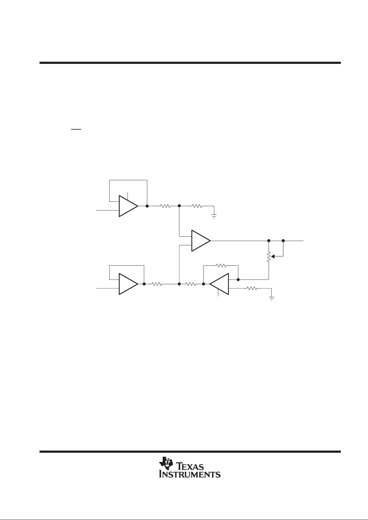
TL03x, TL03xA, TL03xY
ENHANCED-JFET LOW-POWER LOW-OFFSET
OPERATIONAL AMPLIFIERS
SLOS180B – FEBRUARY 1997 – REVISED FEBRUARY 1999
55
POST OFFICE BOX 655303 • DALLAS, TEXAS 75265
APPLICATION INFORMATION
instrumentation amplifier with linear gain adjust
The low offset voltage and low power consumption of the TL03x provide an accurate but inexpensive
instrumentation amplifier (see Figure 70). This particular configuration offers the advantage that the gain can
be linearly set by one resistor:
V
O
=
R6
R5
× (V
B
– VA)
Adjusting R6 varies the gain. The value of R6 always should be greater than, or equal to, the value of R5 to
ensure stability. The disadvantage of this instrumentation amplifier topology is the high degree of CMRR
degradation resulting from mismatches between R1, R2, R3, and R4. For this reason, these four resistors
should be 0.1%-tolerance resistors.
+
–
U1C
+
–
U1A
R6
1 MΩ
V
A
V
CC+
V
O
+
–
+
–
V
B
U1B
R2
10 kΩ
0.1%
R4
10 kΩ
0.1%
R7
100 kΩ
R5
100 kΩ
R1
10 kΩ
0.1%
R3
10 kΩ
0.1%
U1D
V
CC–
NOTE A: U1A through U1D = TL03x; V
CC±
= ±15 V .
Figure 70. Instrumentation Amplifier With Linear Gain-Adjust Circuit

IMPORTANT NOTICE
T exas Instruments and its subsidiaries (TI) reserve the right to make changes to their products or to discontinue
any product or service without notice, and advise customers to obtain the latest version of relevant information
to verify, before placing orders, that information being relied on is current and complete. All products are sold
subject to the terms and conditions of sale supplied at the time of order acknowledgement, including those
pertaining to warranty, patent infringement, and limitation of liability.
TI warrants performance of its semiconductor products to the specifications applicable at the time of sale in
accordance with TI’s standard warranty. Testing and other quality control techniques are utilized to the extent
TI deems necessary to support this warranty. Specific testing of all parameters of each device is not necessarily
performed, except those mandated by government requirements.
CERT AIN APPLICATIONS USING SEMICONDUCTOR PRODUCTS MAY INVOLVE POTENTIAL RISKS OF
DEATH, PERSONAL INJURY, OR SEVERE PROPERTY OR ENVIRONMENTAL DAMAGE (“CRITICAL
APPLICATIONS”). TI SEMICONDUCTOR PRODUCTS ARE NOT DESIGNED, AUTHORIZED, OR
WARRANTED TO BE SUITABLE FOR USE IN LIFE-SUPPORT DEVICES OR SYSTEMS OR OTHER
CRITICAL APPLICATIONS. INCLUSION OF TI PRODUCTS IN SUCH APPLICA TIONS IS UNDERSTOOD T O
BE FULLY AT THE CUSTOMER’S RISK.
In order to minimize risks associated with the customer’s applications, adequate design and operating
safeguards must be provided by the customer to minimize inherent or procedural hazards.
TI assumes no liability for applications assistance or customer product design. TI does not warrant or represent
that any license, either express or implied, is granted under any patent right, copyright, mask work right, or other
intellectual property right of TI covering or relating to any combination, machine, or process in which such
semiconductor products or services might be or are used. TI’s publication of information regarding any third
party’s products or services does not constitute TI’s approval, warranty or endorsement thereof.
Copyright 1999, Texas Instruments Incorporated
 Loading...