

Texas Instruments TICPAL22V10Z-25CFN, TICPAL22V10Z-25CNT Datasheet
TICPAL22V10Z-25C, TICPAL22V10Z-30I
EPIC CMOS PROGRAMMABLE ARRAY LOGIC CIRCUITS
SRPS007C – D3323, SEPTEMBER 1989 – REVISED FEBRUARY 1992
• 24-Pin Advanced CMOS PLD
• Virtually Zero Standby Power
• Propagation Delay Time:
I, I/O to I/O in the Turbo Mode
-25C . . . 25 ns Max
-30I . . . 30 ns Max
I, I/O to I/O in the Zero-Power Mode
-25C . . . 35 ns Max
-30I . . . 40 ns Max
CLK to Q
-25C . . . 15 ns Max
-30I . . . 20 ns Max
• Variable Product Term Distribution Allows
More Complex Functions to Be
Implemented
• Each Output Is User-Programmable for
Registered or Combinatorial Operation,
Polarity, and Output Enable Control
• Extra Terms Provide Logical Synchronous
Set and Asynchronous Reset Capability
• Preload Capability on All Registered
Outputs Allow for Improved Device Testing
• UV Light Erasable Cell Technology Allows
for:
Reconfigurable Logic
Reprogrammable Cells
Full Factory Testing for High
Programming Yield
• Programmable Design Security Bit
Prevents Copying of Logic Stored in Device
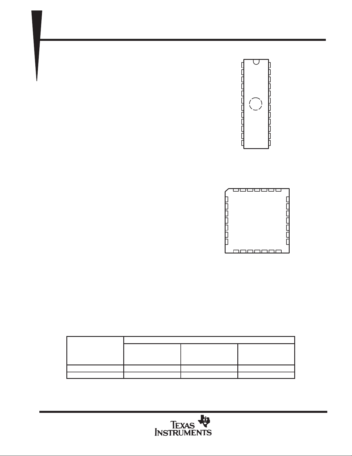
JTL AND NT PACKAGE
(TOP VIEW)
NC
24
23
22
21
20
19
18
17
16
15
14
13
V
I
CC
V
CC
I/O/Q
I/O/Q
I/O/Q
I/O/Q
I/O/Q
I/O/Q
I/O/Q
I/O/Q
I/O/Q
I/O/Q
I
I/O/Q
25
24
23
22
21
20
19
I/O/Q
I/O/Q
CLK/I
GND
I
I
I
NC
I
I
I
1
I
2
I
3
I
4
I
5
I
6
I
7
I
8
I
9
I
10
I
11
12
FN PACKAGE
(TOP VIEW)
I
I
CLK/INCI/O/Q
3212827
426
5
6
7
8
9
10
11
12 13
14 15 16 1718
I
I
GND
– No internal connection
NC
Pin assignments in operating mode
I/O/Q
I/O/Q
I/O/Q
NC
I/O/Q
I/O/Q
I/O/Q
• Package Options Include Plastic
Dual-In-Line and Clip Carrier [for
One-Time-Programmable (OTP) Devices]
and Ceramic Dual-In-Line Windowed
Package
.
T
A
RANGE
0°C to 75°C TICPAL22V10Z-25CJTL TICPAL22V10Z-25CNT TICPAL22V10Z-25CFN
–40°C to 85°C NA TICPAL22V10Z-30INT TICPAL22V10Z-30IFN
These devices are covered by U.S. Patent 4,410,987.
EPIC is a trademark of Texas Instruments Incorporated.
PRODUCTION DATA information is current as of publication date.
Products conform to specifications per the terms of Texas Instruments
standard warranty. Production processing does not necessarily include
testing of all parameters.
CERAMIC WINDOWED
DUAL-IN-LINE
POST OFFICE BOX 655303 • DALLAS, TEXAS 75265
AVAILABLE OPTIONS
(JTL)
PACKAGE TYPE
PLASTIC
DUAL-IN-LINE
(NT)
PLASTIC
CHIP CARRIER
(FN)
Copyright 1992, Texas Instruments Incorporated
1

TICPAL22V10Z-25C, TICPAL22V10Z-30I
EPIC CMOS PROGRAMMABLE ARRAY LOGIC CIRCUITS
SRPS007C – D3323, SEPTEMBER 1989 – REVISED FEBRUARY 1992
description
The CMOS PLD devices feature variable product terms, flexible outputs, and virtually zero standby power. It
combines TI’s EPIC (Enhanced Processed Implanted CMOS) process with ultraviolet-light-erasable EPROM
technology. Each output has an output logic macrocell (OLM) configuration allowing for user definition of the
output type. This device provides reliable, low-power substitutes for numerous high-performance TTL PLDs with
gate complexities between 300 and 800 gates.
The TICPAL22V10Z has 12 dedicated inputs and 10 user-definable outputs. Individual outputs can be
programmed as registered or combinational and inverting or noninverting as shown in the OLM diagram. These
ten outputs are enabled through the use of individual product terms
The variable product-term distribution on this device removes rigid limitation to a maximum of eight product
terms per output. This technique allocates from 8 to 16 logical product terms to each output for an average of
12 product terms per output. The variable allocation of product terms allows for far more complex functions to
be implemented in this device than in previously available devices.
With features such as the programmable OLMs and the variable product-term distribution, the TICP AL22V10Z
offers quick design and development of custom LSI functions. Since each of the ten output pins may be
individually configured as inputs on either a temporary or permanent basis, functions requiring up to 21 inputs
and a single output or down to 12 inputs and 10 outputs can be implemented with this device.
Design complexity is enhanced by the addition of synchronous set and asynchronous reset product terms.
These functions are common to all registers. When the synchronous set product term is a logic 1, the output
registers are loaded with a logic 1 on the next low-to-high clock transition. When the asynchronous reset product
term is a logic 1, the output registers are loaded with a logic 0 independently of the clock. The output logic level
after set or reset will depend on the polarity selected during programming.
Output registers of this device can be preloaded to any desired state during testing, thus allowing for full logical
verification during product testing.
The TICP AL22V10Z has internal electrostatic discharge (ESD) protection circuits and has been classified with
a 2000-V ESD rating tested under MIL-STD-883C, Method 3015.6. However, care should be exercised in
handling these devices, as exposure to ESD may result in a degradation of the device parametric performance.
The floating-gate programmable cells allow the devices to be fully programmed and tested before assembly to
assure high field programming yield and functionality . They are then erased by ultraviolet light before packaging.
The TICPAL22V10Z-25C is characterized for operation from 0°C to 75°C. The TICPAL22V10Z-30I is
characterized for operation from –40°C to 85°C.
design security
The ’PAL22V10Z contains a programmable design security cell. Programming this cell will disable the read
verify and programming circuitry protecting the design from being copied. The security cell is usually
programmed after the design is finalized and released to production. A secured device will verify as if every
location in the device is programmed. Because programming is accomplished by storing an invisible charge
instead of opening a metal link, the ’22V10Z cannot be copied by visual inspection. Once a secured device is
fully erased, it can be reprogrammed to any desired configuration.
2
POST OFFICE BOX 655303 • DALLAS, TEXAS 75265
EPIC CMOS PROGRAMMABLE ARRAY LOGIC CIRCUITS
functional block diagram (positive logic)
TICPAL22V10Z-25C, TICPAL22V10Z-30I
SRPS007C – D3323, SEPTEMBER 1989 – REVISED FEBRUARY 1992
CLK/I
C1
1S
R
Output
Logic
Macrocell
EN
EN
EN
EN
EN
EN
EN
EN
EN
EN
I/O/Q
I/O/Q
I/O/Q
I/O/Q
I/O/Q
I/O/Q
I/O/Q
I/O/Q
I/O/Q
I/O/Q
10
10
12
14
16
16
14
12
10
Set
Reset
8
8
1
10
10
&
44 x 132
22
11
I
10
22
denotes programmable cell inputs
POST OFFICE BOX 655303 • DALLAS, TEXAS 75265
3
4
POST OFFICE BOX 655303 • DALLAS, TEXAS 75265
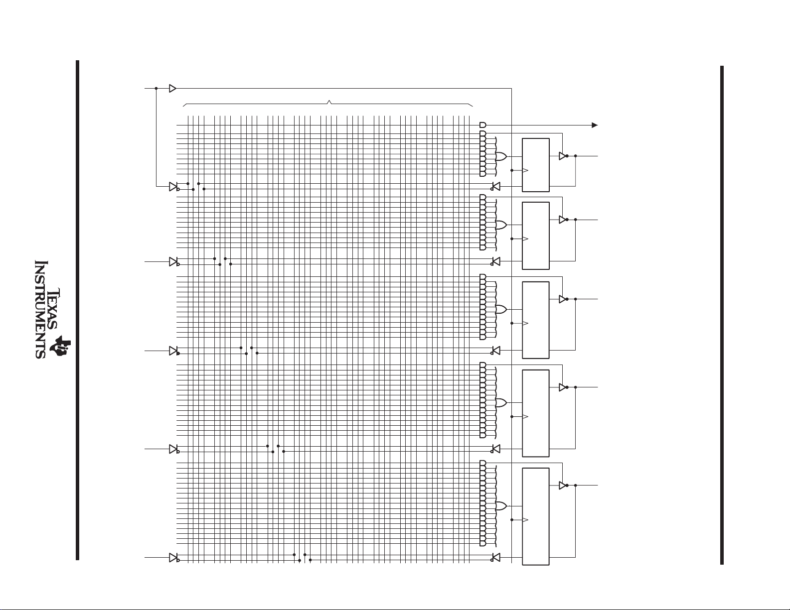
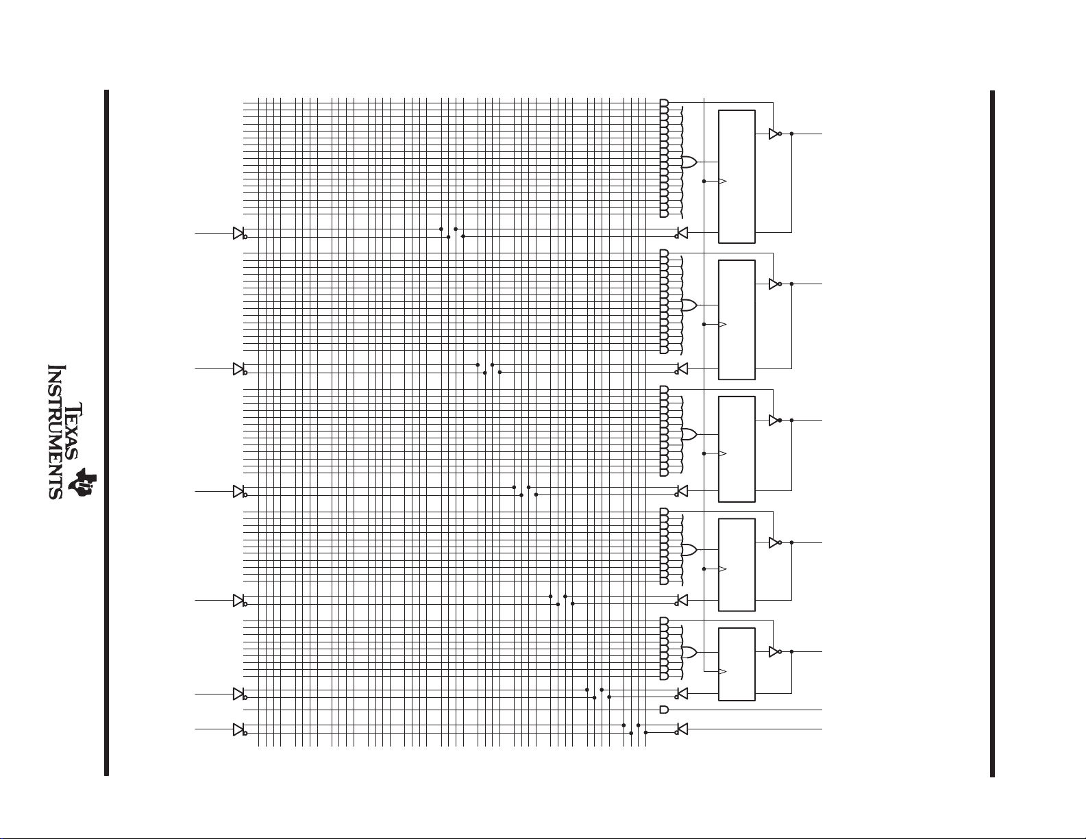
logic diagram (positive logic)
1
CLK/I
First
Cell
Numbers
2
I
3
I
0 481216 20 24 28
0
396
440
880
924
1452
1496
Increment
32 36 40
MACRO
CELL
P = 5808
R = 5809
MACRO
CELL
P = 5810
R = 5811
MACRO
CELL
P = 5812
R = 5813
MACRO
CELL
Asynchronous Reset
(to all registers)
23
I/O/Q
22
I/O/Q
21
I/O/Q
20
I/O/Q
SRPS007C – D3323, SEPTEMBER 1989 – REVISED FEBRUARY 1992
TICPAL22V10Z-25C, TICPAL22V10Z-30I
EPIC CMOS PROGRAMMABLE ARRAY LOGIC CIRCUITS
2112
4
I
2156
2860
5
I
P = 5814
R = 5815
MACRO
CELL
P = 5816
R = 5817
19
I/O/Q
2904
MACRO
CELL
3608
6
I
3652
P = 5818
R = 5819
MACRO
CELL
18
17
I/O/Q
I/O/Q
POST OFFICE BOX 655303 • DALLAS, TEXAS 75265
4268
EPIC CMOS PROGRAMMABLE ARRAY LOGIC CIRCUITS
7
I
4312
4840
8
I
4884
5324
9
I
5368
5720
10
I
5764
11
I
P = 5820
R = 5821
MACRO
CELL
P = 5822
R = 5823
MACRO
CELL
P = 5824
R = 5825
MACRO
CELL
P = 5826
R = 5827
16
I/O/Q
15
I/O/Q
14
I/O/Q
Synchronous Set
(to all registers)
13
I
SRPS007C – D3323, SEPTEMBER 1989 – REVISED FEBRUARY 1992
TICPAL22V10Z-25C, TICPAL22V10Z-30I
5
Inside each MACROCELL the (P) cell is the polarity cell and the (R) cell is the register cell.
Programmable Cell Number = First Cell Number + Increment
TICPAL22V10Z-25C, TICPAL22V10Z-30I
EPIC CMOS PROGRAMMABLE ARRAY LOGIC CIRCUITS
SRPS007C – D3323, SEPTEMBER 1989 – REVISED FEBRUARY 1992
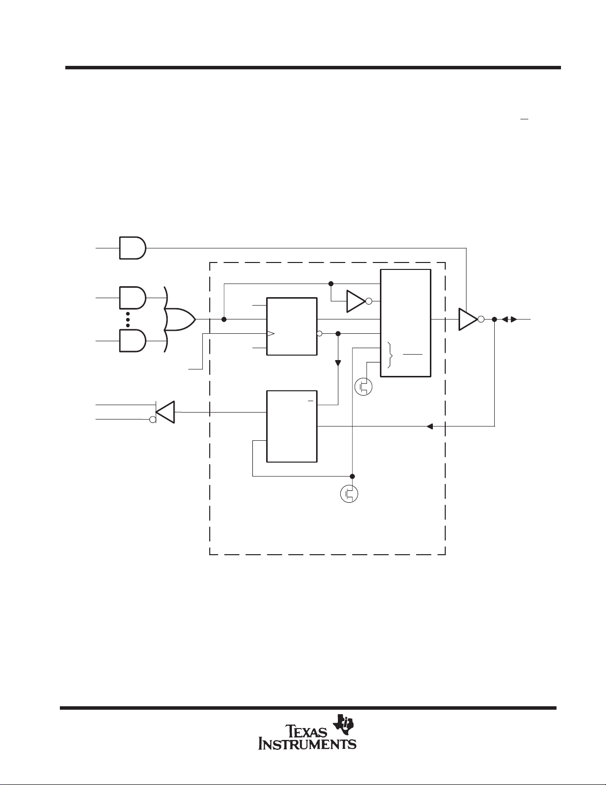
output logic macrocell (OLM) description
A great amount of architectural flexibility is provided by the user-configurable macrocell output options. The
macrocell consists of a D-type flip-flop and two select multiplexers. The D-type flip-flop operates like a standard
TTL D-type flip-flop. The input data is latched on the low-to-high transition of the clock input. The Q and Q outputs
are made available to the output select multiplexer. The asynchronous reset and synchronous set controls are
available in all flip-flops.
The select multiplexers are controlled by programmable cells. The combination of these programmable cells
will determine which macrocell functions are implemented. It is this user control of the architectural structure
that provides the generic flexibility of this device.
output logic macrocell diagram
From Clock Buffer
Output Logic Macrocell
AR
SS
AR = asynchronous reset
SS = synchronous set
R
1D
C1
1S
MUX
1
1
G1
S1
S0
MUX
2
3
0
1
0
1
G
3
0
6
POST OFFICE BOX 655303 • DALLAS, TEXAS 75265
EPIC CMOS PROGRAMMABLE ARRAY LOGIC CIRCUITS
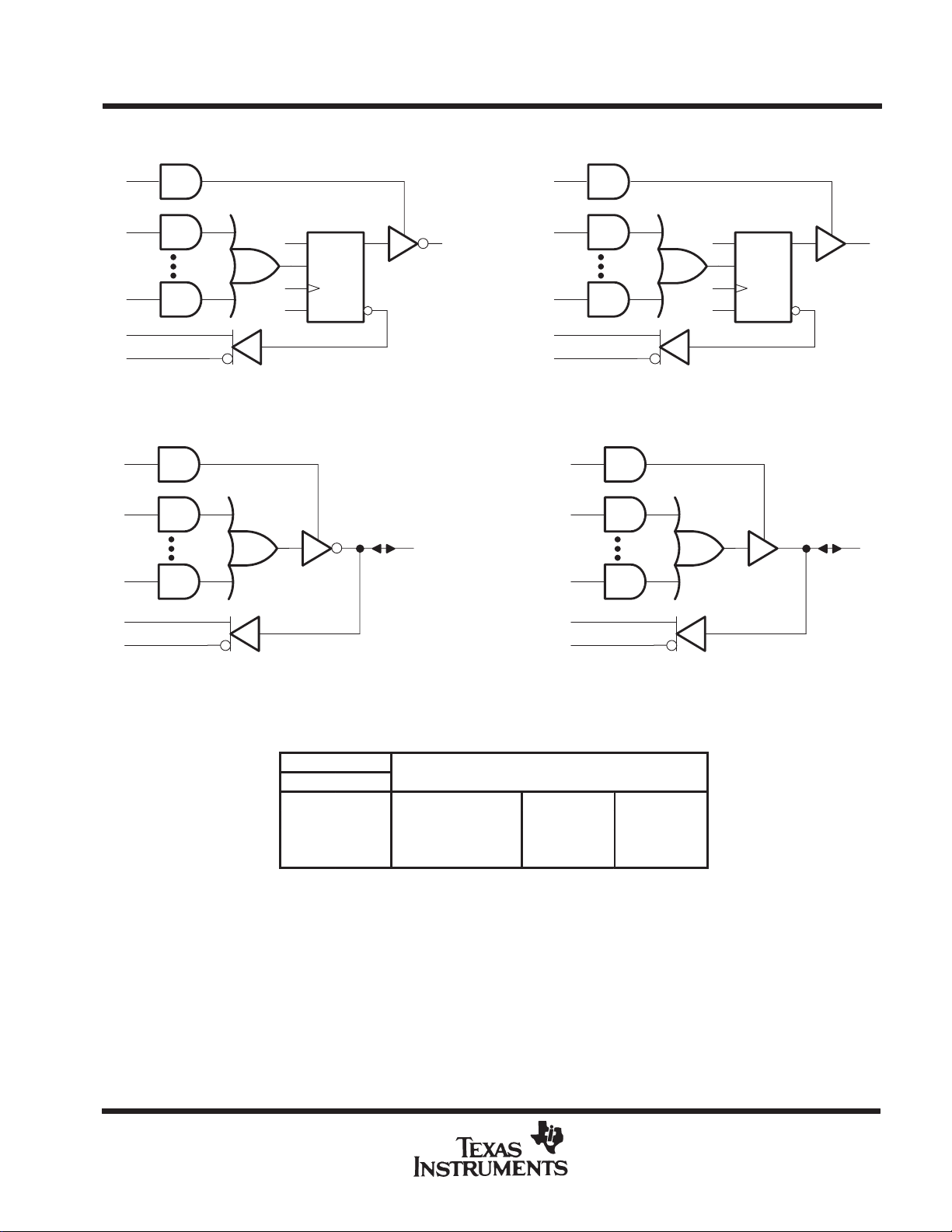
output logic macrocell options (see Figure 1)
TICPAL22V10Z-25C, TICPAL22V10Z-30I
SRPS007C – D3323, SEPTEMBER 1989 – REVISED FEBRUARY 1992
R
1D
C1
1S
REGISTER FEEDBACK, REGISTERED, ACTIVE-LOW OUTPUT REGISTER FEEDBACK, REGISTERED, ACTIVE-HIGH OUTPUT
I/O FEEDBACK, COMBINATIONAL, ACTIVE-LOW OUTPUT I/O FEEDBACK, COMBINATIONAL, ACTIVE-HIGH OUTPUT
S1 = 0
S0 = 0
S1 = 1
S0 = 0
R
1D
1S
C1
S1 = 0
S0 = 1
S1 = 1
S0 = 1
MACROCELL FEEDBACK AND OUTPUT FUNCTION TABLE
CELL SELECT
S1 S0
0 0 Register feedback Registered Active low
0 1 Register feedback Registered Active high
1 0 I/O feedback Combinational Active low
1 1 I/O feedback Combinational Active high
0 = erased cell, 1 = programmed cell
S1 and S0 are select-function cells as shown in the output logic macrocell
diagram.
FEEDBACK AND OUTPUT CONFIGURATION
Figure 1. Resultant Macrocell Feedback and Output Logic After Programming
POST OFFICE BOX 655303 • DALLAS, TEXAS 75265
7
 Loading...