

Page 1

User's Guide
SCPU036–October 2017
TIC12400 Evaluation Module
This user's guide describes the characteristics, operation, and use of the TIC12400 Evaluation Module
(EVM).
Contents
1 Introduction ................................................................................................................... 2
2 Hardware...................................................................................................................... 4
3 SWITCH BOARD Hardware Description ................................................................................. 8
4 GUI Software Installation.................................................................................................. 11
5 TIC12400 GUI Application ................................................................................................ 14
6 Board Files .................................................................................................................. 39
List of Figures
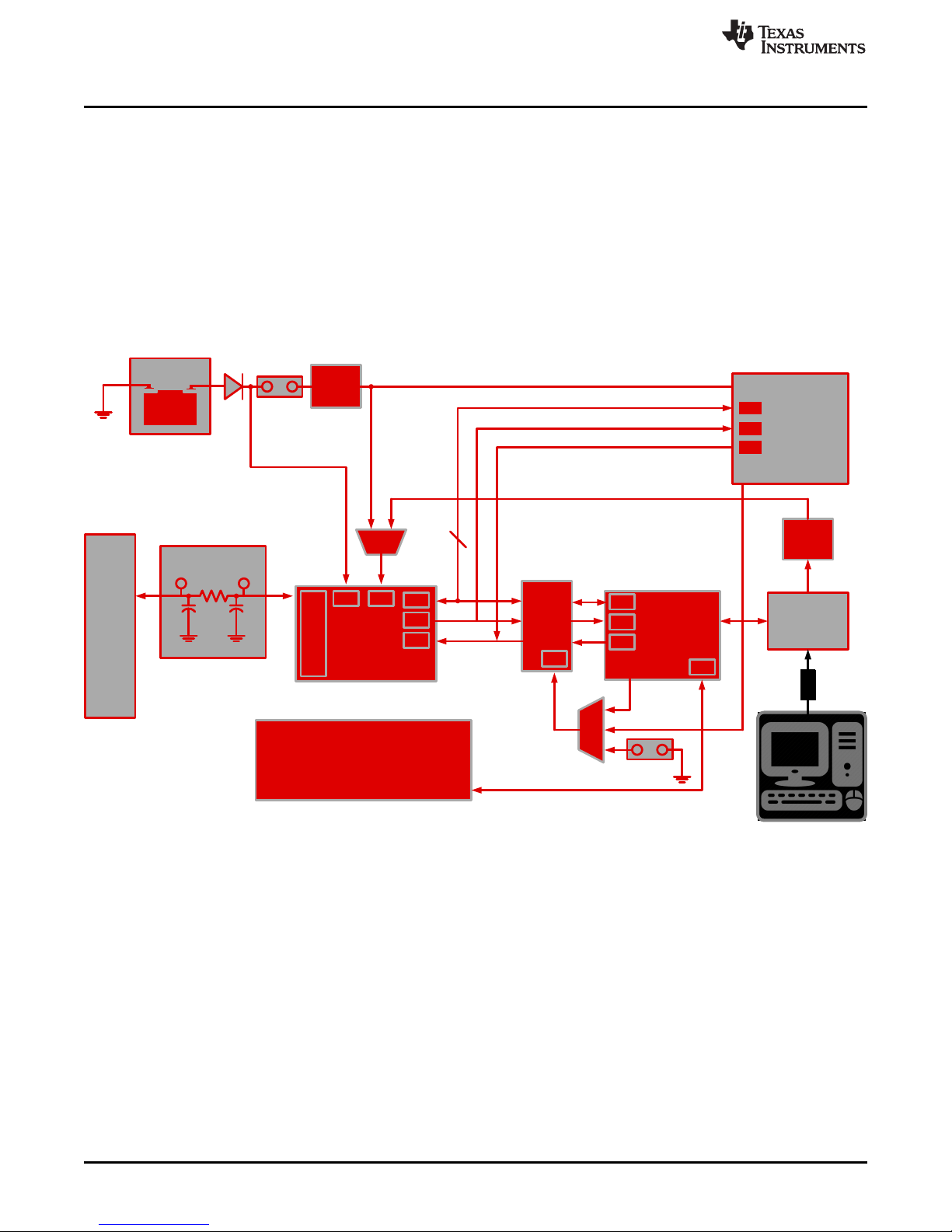
1 TIC12400 EVM Block Level Diagram..................................................................................... 2
2 TIC12400 EVM, SWITCH BOARD, and USB to USB-Mini Cable..................................................... 4
3 EVM, SWITCH BOARD, USB Cable, PC, and Power Supply Setup................................................. 4
4 EVM Hardware Top Description ........................................................................................... 5
5 EVM Hardware Bottom Description ...................................................................................... 6
6 Setup_TIC12400-0.4.0_EVM.exe........................................................................................ 11
7 Installation Steps 1–6...................................................................................................... 12
8 Figure 3. Installation Steps 7–13......................................................................................... 13
9 Double Click on “App Center EVM GUI” Shortcut to Open........................................................... 14
10 GUI Home Page............................................................................................................ 14
11 Device Configuration Page ............................................................................................... 17
12 Channel Configuration Page.............................................................................................. 21
13 Page Connections.......................................................................................................... 39
14 Main Device................................................................................................................. 40
15 USB interface ............................................................................................................... 41
16 <Caption> ................................................................................................................... 41
17 Input filters – IN10-IN23 use 10 Ω instead of 220 Ω................................................................... 41
18 SWITCH Board Schematic................................................................................................ 42
SCPU036–October 2017
Submit Documentation Feedback
Copyright © 2017, Texas Instruments Incorporated
TIC12400 Evaluation Module
1
Page 2
External Micro
Connector
MSP430
(U1)
3.3-V
Regulator
(U4)
IN
x
Connector
Channel
0í23
Battery or Power
Supply
+
_
5-V
Regulator
(U9)
Input Filter
Channel IN0 to IN
23
Test Point Test Point
DNP
TXB0106
(U10)
OE
TIC12400
(U11)
V
DD
V
S
IN
0
IN
1
IN
2
.
.
.
IN
23
SPI
INT
RST
USB
Connector
x24
x4
ONBOARD EVM MONITORS:
x VDD Current Monitor (INA226A, U12)
x VS Current Monitor (INA226A, U13)
x Ambient Air Temp Monitor (TMP102AQ, U5)
x Case Temp Monitor (TMP102AQ, U2)
I2C
D3
SPI
INT
RST
SPI
INT
RST
Copyright © 2017, Texas Instruments Incorporated
Introduction
1 Introduction
The TIC12400 is a multiple switch detection interface that is designed to detect the opening and closing of
up to 24 switch contacts. 10 out of the 24 inputs are configurable to detect switch states that are either
battery connected switches (BCS) or ground connected switches (GCS), which means it can either sink or
source current from the channel. The remaining 14 channels are design to support ground connected
switches only (source current). The wetting current can be preprogrammed to six available values, which
accommodates for different application scenarios. Communication to and from the device is done using a
24-bit SPI protocol.
The TIC124000 and TIC12400-Q1 provide the same functionality and the TIC12400 Evaluation Module is
used for both devices.
www.ti.com
Figure 1. TIC12400 EVM Block Level Diagram
The TIC12400 EVM is an evaluation module for the Texas Instruments TIC12400 and it provides basic
functionality evaluation for the device. When used together with the switch board, the EVM allows testing
of its functionality via SPI communication established to the PC using the USB adaptor.
2
TIC12400 Evaluation Module
Copyright © 2017, Texas Instruments Incorporated
Submit Documentation Feedback
SCPU036–October 2017
Page 3
Caution Hot surface.
Contact may cause burns.
Do not touch.
The DUT of the board can get hot when all channels are enabled at
the highest wetting current settings in continuous mode
www.ti.com
1.1 Warnings
Introduction
SCPU036–October 2017
Submit Documentation Feedback
Copyright © 2017, Texas Instruments Incorporated
TIC12400 Evaluation Module
3
Page 4
+12.0 V
PC
Power
Supply
EVMSWITCH BOARD
USB
Hardware
2 Hardware
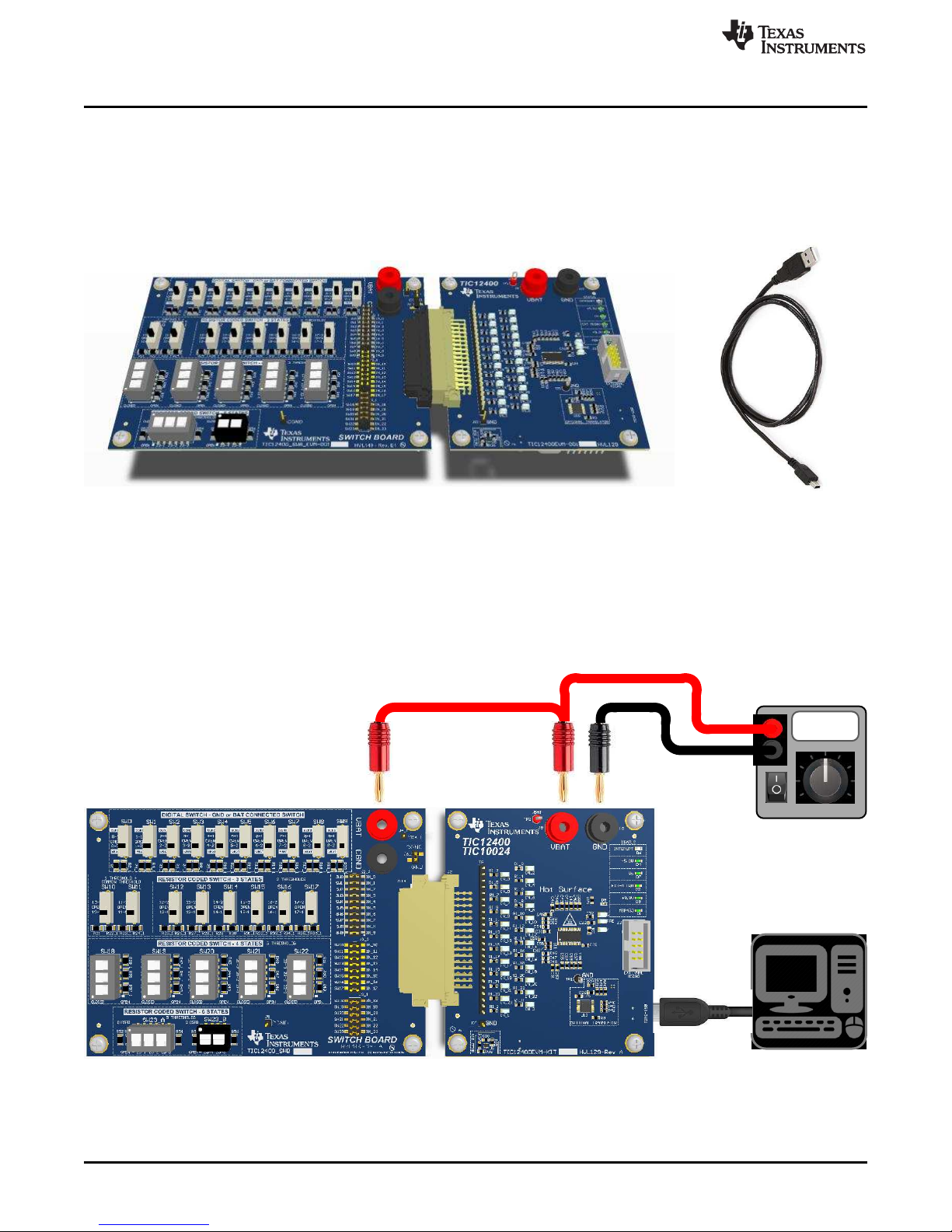
2.1 Kit
Two boards, EVM (TIC12400EVM) and SWITCH BOARD (TIC12400_SWB), are provided with an USB to
USB-MINI cable within the KIT; see Figure 2.
www.ti.com
Figure 2. TIC12400 EVM, SWITCH BOARD, and USB to USB-Mini Cable
2.2 Connection to the PC and Powering up the EVM
A mini-USB cable is used to connect the EVM board to the PC. The VDD of the EVM is powered by the
USB’s VBUS. The positive terminal of the Power Supply is connected to the “VBAT” terminal of both the
EVM and SWITCH BOARD. The negative terminal of the power supply is connected to the “GND” terminal
of the EVM. Turn ON the power supply and set it to a nominal supply of +12 V, see Figure 3.
Figure 3. EVM, SWITCH BOARD, USB Cable, PC, and Power Supply Setup
4
TIC12400 Evaluation Module
Copyright © 2017, Texas Instruments Incorporated
SCPU036–October 2017
Submit Documentation Feedback
Page 5
Optional Circuitry or Functions
Required Circuitry
5
6
1
8
2
9
3
10 11
4
7
www.ti.com
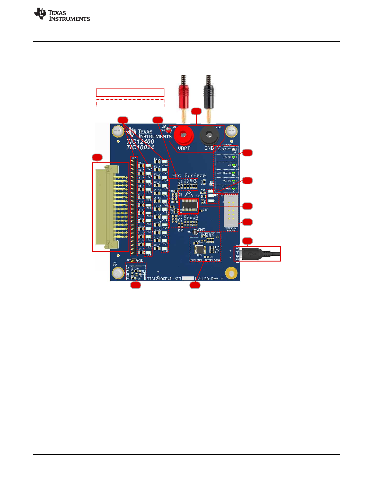
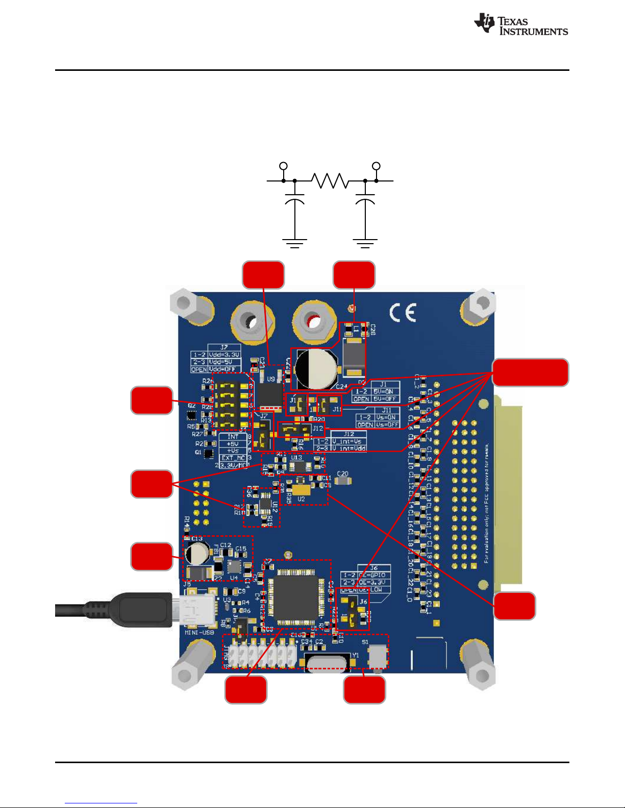
2.3 EVM Hardware Description
The TIC12400 EVM is designed to allow the user to easily evaluate switch detection using the GUI. The
break down of all the features and design of the EVM follow.
Hardware
1. Connect the TIC12400EVM to a supply using VBAT (J9) as the positive terminal of the supply and
GND (J10) to the negative terminal of the supply using standard banana cables. The supply can range
from 4.5V to 35V, but is nominally at 12V.
2. Connect the TIC12400EVM to your computer via the mini-USB cable provided. The actual connector is
located on the bottom side of the board. This will allow your computer to interface with the EVM and
communicate to the device.
3. Connect the Switch Board or your own switches via a mating connector to J2, which connects the
switches to the INx pins of the device.
4. U11 is the TIC12400 devices.
5. The EVM has several LED use to help the user indicate the status of the EVM
6. The device has three post regulator decoupling caps: V
at each output capacitor for each of these three regulators.
7. The EVM facilitates the use of an external microcontroller by interfacing with SPI, INT, and RESET
pins of the device.
8. There is an optional Translator/Level shifter (TXB0106) on the EVM to ensure the ability to interface
with the device's SPI, INT, and RESET functions at various voltages set by VDD pin. The MSP430 is a
3.3-V device and does not support 5-V logic level without the TXB0106.
9. The EVM has the ability to do relative temperature measurements of the air using the TI TMP0104AQ
SCPU036–October 2017
Submit Documentation Feedback
Figure 4. EVM Hardware Top Description
, V
CAP_D
CAP_PRE
Copyright © 2017, Texas Instruments Incorporated
, and V
TIC12400 Evaluation Module
. There are test points
CAP_A
5
Page 6
19
2
1,6,7,11,12
7
8
6
45
3
TP
IC
TP
CONNECTOR
Hardware
10. There are place holders for a filter components on each channel of the EVM. There is a 100mil header
11. The filter capacitors at the pins of the device are not loaded by default and are there to allow the
www.ti.com
device.
along the edge of the connector to measure signal at connector, and SMT test points to measure the
signal at the IC.
design of filters if needed.
6
TIC12400 Evaluation Module
Figure 5. EVM Hardware Bottom Description
Copyright © 2017, Texas Instruments Incorporated
SCPU036–October 2017
Submit Documentation Feedback
Page 7

www.ti.com
1. The EVM has a blocking diode and large bulk capacitor. The blocking diode (D3) protects the EVM in
2. The EVM has the ability to do relative temperature measurements of the device's case temperature
3. The MSP430's support devices, such as JTAG interface, crystal, programming button, and so forth.
4. The MSP430 bridges the communication from the computer’s USB cable to the device's SPI, INT, and
5. The TPS73533 receives power from the VBUS of the USB, which is 5 V. It then regulates that to the
6. There are two INA226A Current Monitors for measuring current in VDD (U12) and for measuring th
7. There are four status LED on the EVM that take up power when in use. The header (J4) facilitates
8. The TPS7A6650Q is a high voltage regulator that is able to take high voltage and regulate it down to
Hardware
case the terminals of the battery are switched accidentally. The bulk capacitor (C24) adds a delay
between a battery disconnect and the device shutting down.
a. 2.1 There EVM has several jumpers for configuring the EVM in a variety of ways. J1: This jumper
connects the input of the 5V regulator to VS if inserted. (Default: Not Loaded)
b. 2.6 J6: This jumper connects a GPIO from the EVM micro (MSP430) to the output enable (OE) of
the TXB0106 level shifter by placing the jumper between pins 1 and 2. Placing the jumper between
pins 2 and 3 forces the translator to be on. If there is no jump on J7 then the pull down resistor
turns it off (OE=LOW) and places the level shifter in high impedance mode, preventing bus
contention between two possible masters on the SPI bus.
c. 2.7 J7: This jumper connects VDD pin of the device to either the onboard +3.3V supply generated
from the USB bus or connects to the onboard +5V regulator that is supplied from the battery.
Connecting pin 1 and 2 with a jumper connects VDD to +3.3V and connecting 2 and 3 with a
jumper connects VDD to +5V (this assumes J1 is also loaded). (Default: jumper across pin 1 and
2)
d. 2.11 J11: This jumper connects VS pin of the device to the bulk capacitor after the protection
diode.
e. 2.12 J12: This jumper gives the option of having the pull up resistor come from either VDD or VS.
Connecting pin 1 and 2 with a jumper, references the INT pin to VS. Connecting pin 2 and 3 with a
jumper references the INT pin to VDD.
using TI’s TMP0104AQ device.
RESET lines. The MSP430 also interfaces with several supports circuits for measuring temperature for
air and case, measuring current to VDD, and measuring current to VS. The MSP430 also has the
ability to control OE pin of TXB0106 to facilitate control of the device by an external microcontroller.
+3.3V output on the TIC12400 EVM.
current going into VS (U13). The MSP430 interfaces with these devices using I2C and relays the
information through the UBS cable to the GUI on the computer.
removing the LED’s in the circuit to do system level power measurements accurately.
5V for use with higher voltage micro controllers. When J1 is removed the regulator’s input voltage is
removed and therefore it is disabled.
SCPU036–October 2017
Submit Documentation Feedback
Copyright © 2017, Texas Instruments Incorporated
TIC12400 Evaluation Module
7
Page 8
23-1 23-2 23-3 23-4 23-5
SW23_A
SW23_B
IN23
29
3
8
7
6
5 4
1
SWITCH BOARD Hardware Description
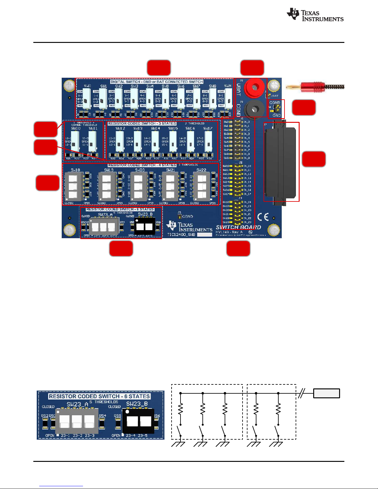
3 SWITCH BOARD Hardware Description
www.ti.com
1. The SWITCH BOARD (SWB) is designed such that ground offsets can be tested by removing J6,
which disconnects the Chassis Ground (CGND) from the EVM ground (GND). A supply can be placed
between GND and CGND to create the offset. If not testing this feature, then J6 is by default in place
and therefore CGND and GND are shorted together.
2. VBAT provides the power to the battery connected switches. Switch 0 to 9 are battery connected
switches.
3. J114 connects all the switches from the SWB to the inputs of the EVM.
4. J1, J2, and J3 are jumpers that connect SW0 to SW23 to IN0 to IN23 of the EVM. These jumpers
allow the user to disconnect the SW’s on the Switch Board to the EVM and provide a 0.1" head to
connect their own switch of their choosing to the EVM.
5. SW23A and SW23B are provided to test the device's ability to detect multi-resistor coded ground
referenced switch transitions. SW23A relate directly to the mapped thresholds for 3A, 3B, and 3C.
SW23B relate directly to thresholds 8 and 9 of the device. Switch 23-1-5 are designed to coincide with
one state for each instance of one switch being in the “CLOSED” position. Channel 23 of the device
has the ability to set up to 5 thresholds, which means there are 6 states. Each switch represents one
state and all switches in the “OPEN” position represents the 6th state.
8
TIC12400 Evaluation Module
Copyright © 2017, Texas Instruments Incorporated
SCPU036–October 2017
Submit Documentation Feedback
Page 9
X-2
OPEN
X-1
X-2
OPEN
X-1
X-2
OPEN
X-1
X-1 X-2
SWX
INX
OPEN
X-2
OPEN
X-1
X-2
OPEN
X-1
X-2
OPEN
X-1
X-1 X-2
SWX
INX
OPEN
X-1 X-2 X-3
SWX
IN_X
www.ti.com
6. SW18 – SW22 are used to test up to 4 state resistor coded ground referenced switches. Each of the
7. SW12 – SW17 are used when up to two thresholds (three states) is needed for the switch application.
SWITCH BOARD Hardware Description
channels have three ground connected switches labeled X-1, X-2, and X-3, which coincides with a
mapped threshold for 3A, 3B, and 3C. Each individual switch represents one of the three states and
the fourth state is when all switches are “OPEN”.
Each of the channels have two ground connected switches labeled X-1 and X-2, which coincides with
a mapped threshold for 2A and 2B, and a switch position called “OPEN” to represent the third state.
8. SW10 and SW11 are used when up to two thresholds (three states) is needed for the switch
application. Each channel from 0 to 11, has one unique threshold mapping for each channel and one
common threshold (THRES_COM) that is shared for all the channels (0-11). These switches are setup
to illustrate this feature.
SCPU036–October 2017
Submit Documentation Feedback
Copyright © 2017, Texas Instruments Incorporated
TIC12400 Evaluation Module
9
Page 10
X-1
OPEN
X-2
OPENOPEN
SWX
X-1
X-2
OPEN
VBAT
IN_X
X-1
X-2
X-1
X-2
SWITCH BOARD Hardware Description
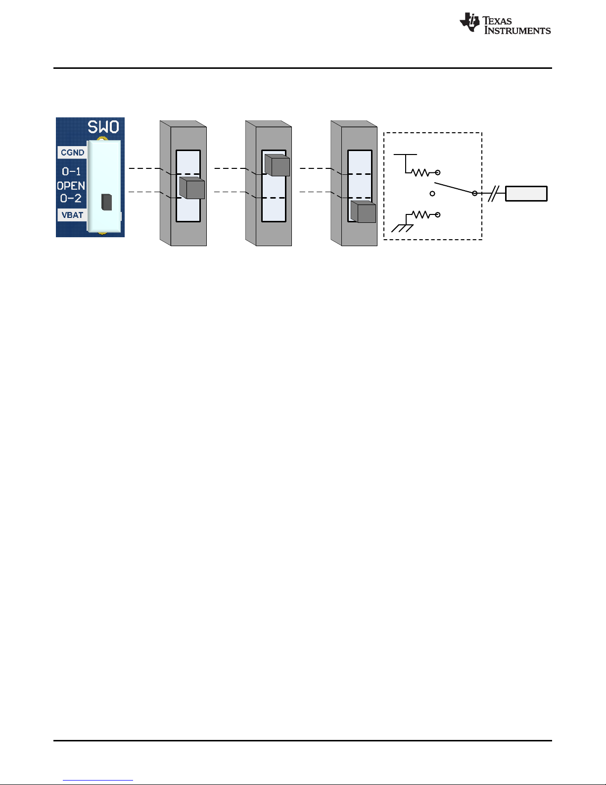
9. SW0 to SW9 are designed to test the device ability to detect digital switches that are either referenced
to a battery connected switch or ground connected switch. There are two state, “OPEN” and either
chassis Ground Connected Switch (GCS) or Battery Connected Switch (BCS).
www.ti.com
10
TIC12400 Evaluation Module
Copyright © 2017, Texas Instruments Incorporated
SCPU036–October 2017
Submit Documentation Feedback
Page 11

www.ti.com
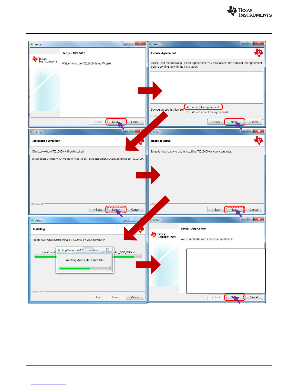
4 GUI Software Installation
The GUI software is required to establish the communication between the EVM boards and the PC and it
also provides the GUI interface to read/write registers information on device. The following section
described the software installation procedure.
Step 1. Download the GUI software
The software can be downloaded on TI server at link goes here. Please inquiry with a TI representative
if you don’t have access to the files.
Step 2. Software installation
Go to location that the executable was downloaded to and either double-click the Setup_TIC12400-
0.4.0_EVM.exe file to begin software installation or right click and select “Run as administrator”. The
software will install two applications, “App Center” software and the TIC12400 GUI App software. If the
“App Center” software isn’t already installed on the PC then additional steps will be needed. Those
steps are outlines in the following figures.
GUI Software Installation
Follow the on-screen instructions to complete the setup. The process may take up to 10 minutes
depending on your computer speed.
SCPU036–October 2017
Submit Documentation Feedback
Figure 6. Setup_TIC12400-0.4.0_EVM.exe
Copyright © 2017, Texas Instruments Incorporated
TIC12400 Evaluation Module
11
Page 12
This screen should show up shortly after step
5. This screen should appear on top, unless the
user clicks on another item. Sometimes the
screen may appear to be behind the other
setup screen. The TIC12400 EVM GUI will not
install until the App Center software is first
installed.
GUI Software Installation
www.ti.com
12
TIC12400 Evaluation Module
Figure 7. Installation Steps 1–6
Copyright © 2017, Texas Instruments Incorporated
SCPU036–October 2017
Submit Documentation Feedback
Page 13
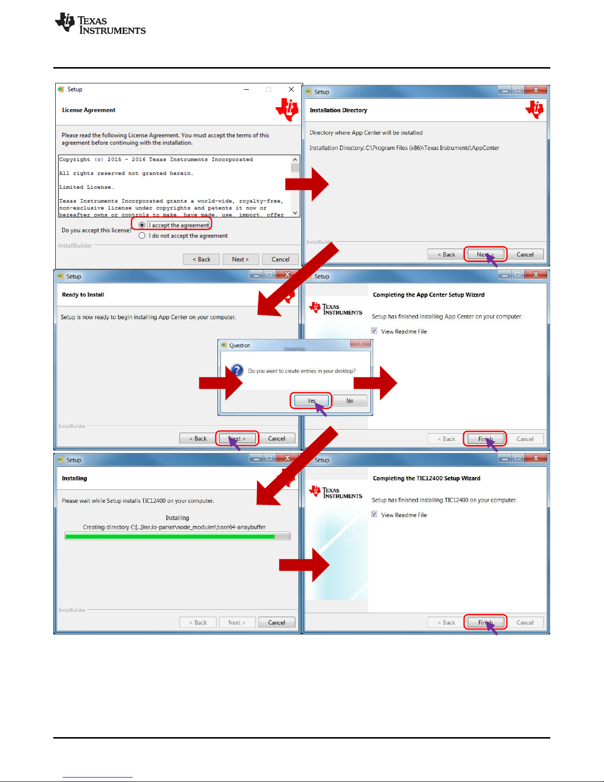
www.ti.com
GUI Software Installation
The EVM GUI can either be opened before or after the EVM is setup and power is applied.
SCPU036–October 2017
Submit Documentation Feedback
Figure 8. Figure 3. Installation Steps 7–13
Copyright © 2017, Texas Instruments Incorporated
TIC12400 Evaluation Module
13
Page 14
10
2
1
9
3 4 5 6
7
8
TIC12400 GUI Application
5 TIC12400 GUI Application
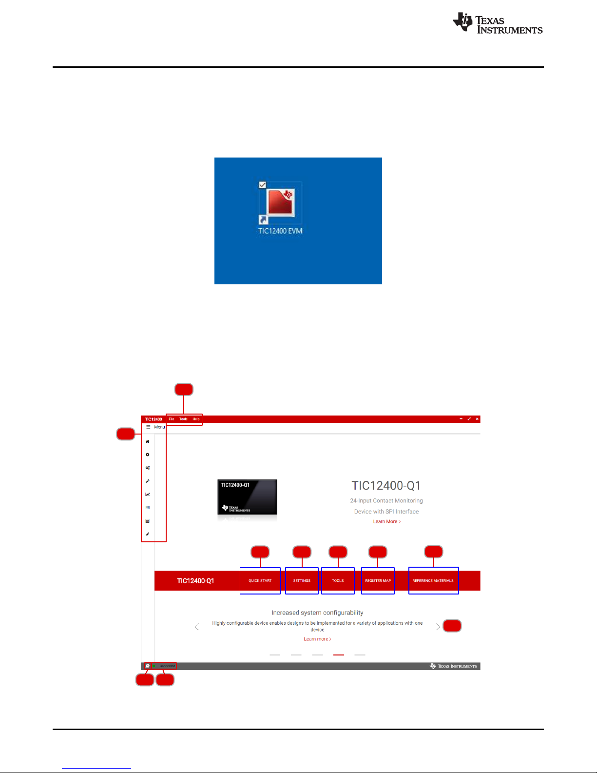
5.1 Starting the GUI
After the EVM and SWITCH BOARD are connected and then the cables are connected the Power Supply
and PC via USB cable, the GUI can be run by double clicking the shortcut icon on the desktop, see
Figure 9.
Figure 9. Double Click on “App Center EVM GUI” Shortcut to Open
5.2 TIC12400 Info Page
The “Info” page (Home) of the TIC12400 GUI has a short summary of the features of the TIC12400. See
the following map of features of the “Info” page in Figure 10.
www.ti.com
14
TIC12400 Evaluation Module
Figure 10. GUI Home Page
Copyright © 2017, Texas Instruments Incorporated
SCPU036–October 2017
Submit Documentation Feedback
Page 15
www.ti.com
TIC12400 GUI Application
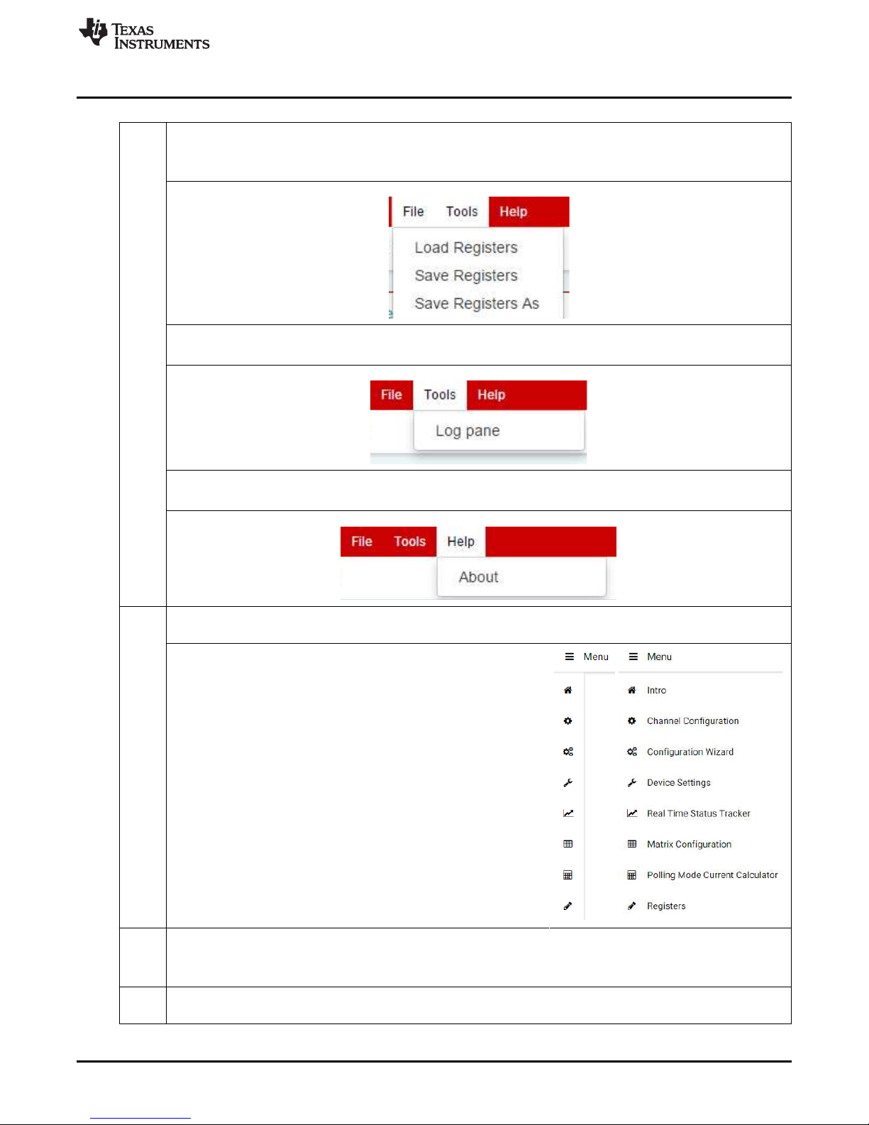
The Menu bar has several sub menus that are within “File”, “Tools” and “Help” drop down menus.
“File” drop down menu provides access to “Saving Registers”, “Save Registers As”, and “Load
Registers”. This means switch profiles can be saved and loaded as needed.
“Tools” drop down menu provides access to the Logging feature of the GUI. This records both
SPI Reads and Writes.
1.
“Help” drop down menu provides access to information pertaining to GUI version and MSP430
firmware revision.
The Menu bar can be clicked to show the minimized and maximized menu, default is minimized.
The buttons on the bar are from top to bottom as follows:
• Intro (Home): Brings the user back to the Intro screen
• Channel Configuration: Page to configure the channels
of the device in a graphical format
• Configuration Wizard: Guided setup of MSDI based on
system level requirements
• Device Settings: Access device settings without manually
2.
adjusting the register settings
• Real Time Status Tracker: Live visual monitoring of
channel inputs
• Matrix Configuration: Graphical configuration of the
Matrix mode settings
• Polling mode current calculator: Page to calculate the
current consumption of the devicewhile in polling mode
with multiple settings, and Register Map. These are also
available buttons on the right of the “Intro” page.
• Registers: Register access page
Quick Start. Opens up a sub menu with two options.
3.
1. A configuration wizard that walks through the system level use case to setup the device
2. Load default configuration for the device
The settings button will open a sub menu for Channel Configurations, Device Settings and Matrix
4.
configuration. These are the same pages accessed by the men bar on the left side of the GUI.
SCPU036–October 2017
Submit Documentation Feedback
Copyright © 2017, Texas Instruments Incorporated
TIC12400 Evaluation Module
15
Page 16
TIC12400 GUI Application
The tools button will open a sub menu to access the Polling Mode current Calculator and Real-
5.
Time Status Tracker pages.
6. Clicking on the register map button will direct the user to the Register map page via a sub menu.
Reference materials button that pulls up links to the EVM User’s Guide, Datasheet and a
7.
reference video.
Benefits banner. Clicking on the links in this section will show greater details on the device
8.
benefits and how they differ from today’s implementations.
The button toggles ON/OFF the Log page, which is also seen in the Tools->Log pane.
9.
If the EVM is connected to the PC with the USB cable then the GUI will show that it is connected
by showing a green dot. If there is no communication with either the on board micro controller
(MSP430) or the device then the following image will be seen, indicated no communication.
10.
www.ti.com
16
TIC12400 Evaluation Module
Copyright © 2017, Texas Instruments Incorporated
SCPU036–October 2017
Submit Documentation Feedback
Page 17

1
6
7
12
11
10
9
2
3
4
5
8
www.ti.com
5.3 Device Settings Page
The Device Configuration page controls many of the features for TIC12400 that control device general
operation.
TIC12400 GUI Application
Figure 11. Device Configuration Page
SCPU036–October 2017
Submit Documentation Feedback
Copyright © 2017, Texas Instruments Incorporated
TIC12400 Evaluation Module
17
Page 18

)
)
)
)
TIC12400 GUI Application
The device has a variety of setting and features that are accessed and controlled by doing read
and writes to the device. It is important to note that when selecting and changing setting within
the GUI it must be written to the device prior to initiating the activation of the device by clicking on
the “Trigger” button. Once the Trigger is turned ON all registers become read only (with the
exception of the CRC_T, RESET, and TRIGGER bits). Trigger initiates the wetting currents and
1.
starts external switch monitoring.
The device has several features that help ensure robust communications to and from the device
to the micro controller on the SPI bus. Interrupts can be generated in the INT pin of the device to
communicate to the user that either “SPI_FAIL”, “PARITY_FAIL”, or “CRC_CALC_COMPLETE”
fault has occurred.
2.
The device has the ability to alert the user when Switch State Change (SSC) has occurred. The
Channel Configuration sets the conditions that initiate a SSC. If this feature is not selected then
the SSC is recorded but the INT pin is not asserted. This is also true for the VS0 and VS1 voltage
state change. There are four different thresholds (VS0_THRES2A/B and VS1_THRES2A/B) that
can be set for VS measurements to establish state changes. If the VS0/VS1 Threshold Crossing
features are not selected then the INT pin is not asserted after a state change, but it will be
3.
stored in the device and the user must read the device to determine that the a state change
occurred.
www.ti.com
If the "Wetting Current Diag" is selected then an INT assertion occurs if any of the "Wetting
Current Diag – IN0/1/2/3" fail. If the "ADC Diag" is selected then an INT is asserted if the ADC
Diag fails
4.
The device has the ability to assert the INT pin when System Faults occur such as “Over
Voltage”, “Under Voltage”, “Temperature Warning”, and “Temperature Shutdown”.
5.
This button sends a software reset to the device via SPI. This will reset all registers to their
default setting! The user must write back all the registers before selecting “Trigger” and to start
wetting current and start external switch monitoring.
6.
18
TIC12400 Evaluation Module
Copyright © 2017, Texas Instruments Incorporated
SCPU036–October 2017
Submit Documentation Feedback
Page 19

*
www.ti.com
TIC12400 GUI Application
The TIC12400 GUI monitors the INT pin approximately at every second. There is an INTERUPT
led on the EVM lights up when the INT pin is asserted. This coincides with the INT icon. Once the
INT is asserted then selecting the READ button reads the INT_STAT register which clears the
INT assert
7.
If the Auto-Read interrupt register features is selected then the GUI will automatically read the
INT_STAT register every 5 seconds, which will clear the INT and record the INT_STATE register
information into GUI, but it does clear the INT_STAT register within the device.
The Wetting Current Auto-Scaling feature allows the user to enable or disable the auto scaling
feature in continuous mode.
8.
The Temperature warning and wetting current reduction feature provides the ability to enable or
disable the wetting current reduction feature when a Temperature warning event occurs.
9.
The TIC12400 has the ability to do an ADC diagnostics and also has the ability to test wetting
currents on IN0, IN1, IN2, and IN3 and diagnose if there are faults.
10.
SCPU036–October 2017
Submit Documentation Feedback
Copyright © 2017, Texas Instruments Incorporated
TIC12400 Evaluation Module
19
Page 20

TIC12400 GUI Application
The TIC12400's advanced settings have several features that allow the user to optimize their
switch state change monitoring system. VS measurement can be enabled or disabled here. Once
enabled the advanced settings menu becomes accessible to the right of the checkbox.
Accessing the VS Measurement settings will allow the user to select the channel, resistor divider
ratio and select the thresholds. The thresholds can be shown in volts or ADC thresholds or volts.
The Operation mode and timing settings can also be configured between polling and continuous
mode.
www.ti.com
Clicking the Settings cog opens the timing settings menu to configure the polling mode.
11.
The CCP or clean current polling settings can also be configured by clicking the configure CCP
option. This will allow the user to enable CCP by channel and select the current to be either 10
mA or 15 mA by group.
Additional the detection filter can be adjusted and the Interrupt assertion scheme can be
selected.
20
TIC12400 Evaluation Module
Copyright © 2017, Texas Instruments Incorporated
SCPU036–October 2017
Submit Documentation Feedback
Page 21

*
1
5
4
2
3
* *
www.ti.com
CRC calculations can be initiated and results displayed within this window. Note, an INT can be
setup to indicate when the CRC calculation is completed by the device, which at that time it can
be read.
12.
Displayed results will look as follows:
5.4 Channel Configuration Page
The Channel Configuration page controls the Channel settings for how to indicate state change when
monitoring the Channels.
TIC12400 GUI Application
The TIC12400 has a variety of setting and features that are accessed and controlled by doing
read and writes to the device. It is important to note that when selecting and changing setting
within the GUI it must be written to the device prior to initiating the activation of the device by
clicking on the “Trigger” button. Once the Trigger is turned ON all registers become read only
(with the exception of the CRC_T, RESET, and TRIGGER bits). Trigger initiates the wetting
1.
currents and starts external switch monitoring.
SCPU036–October 2017
Submit Documentation Feedback
Figure 12. Channel Configuration Page
Copyright © 2017, Texas Instruments Incorporated
TIC12400 Evaluation Module
21
Page 22

*
*
SOURCE
Wetting Current Direction
SINK
Wetting Current Direction
*
TIC12400 GUI Application
The TIC12400 has 24 channels that can be configured a variety of ways to detect all types of
switches. Within the “Simple View” the GUI breaks down each channel into manageable easy to
visualize channel settings. In order to change the setting the Channel must be Enabled, which is
done by clicking on the Enable/Disable button. The channel will no longer be greyed out and
channel information will be able to be changed.
Each Column describes the feature that can be changed and a simple single click will toggle
between settings or allow to select from a drop down menu.
2.
www.ti.com
More advanced setting for each Channel can be accessed clicking on the settings icon.
22
TIC12400 Evaluation Module
Copyright © 2017, Texas Instruments Incorporated
SCPU036–October 2017
Submit Documentation Feedback
Page 23

*
www.ti.com
TIC12400 GUI Application
The GUI monitors the INT pin approximately at every second. There is an INTERUPT led on the
EVM lights up when the INT pin is asserted. This coincides with the INT icon. Once the INT is
asserted then selecting the READ button reads the INT_STAT register which clears the INT
assert
3.
If the Auto-Read interrupt register features is selected then the GUI will automatically read the
INT_STAT register every 5 seconds, which will clear the INT and record the INT_STATE register
information into GUI, but it does clear the INT_STAT register within the device.
All the Channels can be Enabled or Disabled all at once by clicking on these buttons.
4.
SCPU036–October 2017
Submit Documentation Feedback
Copyright © 2017, Texas Instruments Incorporated
TIC12400 Evaluation Module
23
Page 24

*
*
*
TIC12400 GUI Application
The TIC12400 Channel Configurations can be controlled by one of three ways.
1) "Simple View" is the default mode of accessing the Channel Configurations if
2) "Detailed View" allows the user to see all the Channel Configurations at once and also to
design to show all the dependent variables.
www.ti.com
5.
3) Register Map view allows the user to do individual bit control for configuration registers.
24
TIC12400 Evaluation Module
Copyright © 2017, Texas Instruments Incorporated
SCPU036–October 2017
Submit Documentation Feedback
Page 25

1
3
2
www.ti.com
5.5 Channel Configuration Wizard
TIC12400 GUI Application
The TIC12400 GUI will walk through the system configuration with a series of question prompts
1.
on the system configuration. Once a prompt is completed the GUI will move on the to the next
step. You can edit any prompt at any time regardless of your current step in the wizard.
After completing the question prompts. The start button will move to the next area to be
2.
configured.
The red outline will show the current part of the system being addressed by the prompt. As more
3.
questions are answered this area will show how the external system is being interpreted by the
GUI.
SCPU036–October 2017
Submit Documentation Feedback
Copyright © 2017, Texas Instruments Incorporated
TIC12400 Evaluation Module
25
Page 26

1
3
2
TIC12400 GUI Application
www.ti.com
The system configuration from the previous page is shown at the top of the section. Clicking the
Modify button will bring up a prompt to change these settings.
Here is it possible to change of the settings again as necessary for either adding a new switch to
the configuration or adjusting the overall system details. After the desired system configuration is
set, press the Update button to change the setting and click the X to return to the wizard.
1.
Each IWett setting will give a recommended threshold. If the Recommended threshold in N/A that
setting is not recommended.
2. This displays the current global thresholds for the ADC.
26
TIC12400 Evaluation Module
Copyright © 2017, Texas Instruments Incorporated
SCPU036–October 2017
Submit Documentation Feedback
Page 27

1
2
www.ti.com
TIC12400 GUI Application
The wetting current setting can be selected either by using the drop down menu in this section or
clicking the setting in section 1.
Based on the number of switch states the GUI will recommend the appropriate channel that can
handle the switch type.
3.
The Recommended thresholds section will show which thresholds are available to use. It is
important to keep track of the global thresholds that are currently being used by other channels
as the TIC12400 is configured.
After the desired settings are correct, clicking the copy settings will configure the TIC12400
device. Clicking Do Nothing will exit the wizard. The wizard can be used multiple times to update
TIC12400 per each switch in the system.
SCPU036–October 2017
Submit Documentation Feedback
Copyright © 2017, Texas Instruments Incorporated
TIC12400 Evaluation Module
27
Page 28

TIC12400 GUI Application
The current setting and threshold calculations will be different for different switch states. For 4
switch states 3 thresholds must be used. If any of the threshold boxes for a given wetting current
setting are populated with NA, that current setting cannot be used. If all of the current settings
cannot be used the resistance ranges for the switch are not supported. For more information on
the supported resistance values for multiple switch states see the datasheet.
In this example the only supported wetting current is 2 mA as all of the thresholds have values.
1.
In this example the only supported wetting current is 2 mA as all of the thresholds have non NA
values.
www.ti.com
The recommended channels that are available all support the 4 switch configuration and the
channels that do not support 4 switch states are not recommended.
2.
Additionally the available threshold settings are Thres3A/B/C. These thresholds can be mapped
to any unmapped thresholds but must follow the rules that ThresC > ThresB > ThresA.
28
TIC12400 Evaluation Module
Copyright © 2017, Texas Instruments Incorporated
SCPU036–October 2017
Submit Documentation Feedback
Page 29

1
3
2
www.ti.com
5.6 Real Time Status Tracker
TIC12400 GUI Application
The channel list includes all the available channels for the device. Enabled channels display
green and disabled channels display gray. Clicking green channels will turn on the GUI tracker for
that channel. Clicking the same button again will disable the GUI tracker. Note this does not
enable/disable the channel in the device, it changes if the GUI displays any real time changes.
1.
SCPU036–October 2017
Submit Documentation Feedback
Copyright © 2017, Texas Instruments Incorporated
TIC12400 Evaluation Module
29
Page 30

1
3
2
4
TIC12400 GUI Application
This will show each channel that the GUI tracker is enabled for. Each channel will show the
threshold on the left side of the graph. For multiple switch state channels all the thresholds are
shown. As the switch state changes the graph will update accordingly as shown below if the
Trigger has been enabled in section 3.
2.
Clicking the trigger button will enable the device to monitor the inputs and update the real time
status tracker.
3.
www.ti.com
5.7 Matrix Configuration
30
TIC12400 Evaluation Module
Copyright © 2017, Texas Instruments Incorporated
SCPU036–October 2017
Submit Documentation Feedback
Page 31

www.ti.com
TIC12400 GUI Application
The Matrix configuration settings area changes the setup for Matrix mode according to the
system requirements Clicking the Matrix configuration will allow you to select between the
supported configurations.
The input source and sink currents are also selectable via a drop down menu. The sink current
must always be larger than the source current and the GUI will make unusable source and sink
combinations un-selectable.
1.
The detection edge control option lets you select between no detection, rising, falling, and rising
or falling edge detection schemes.
The Matrix polling active time controls how long the inputs are polled as described in the
datasheet.
SCPU036–October 2017
Submit Documentation Feedback
Copyright © 2017, Texas Instruments Incorporated
TIC12400 Evaluation Module
31
Page 32

TIC12400 GUI Application
The Switch Status area shows the current status of the matrix of switches. The status can be
checked by clicking the Check switch status button. Mousing over a box will show which switch
that is.
2.
This is a visual depiction of the matrix mode operation. Selecting the different matrix settings
(4x4, 5x5, 6x6) will change the image to show which channels are being used.
www.ti.com
3.
After setting the desired matrix configuration click the Write to Device button to set the register
4.
settings in the TIC12400 device. Use the Trigger button to monitor the TIC12400 enable
monitoring of the inputs.
32
TIC12400 Evaluation Module
Copyright © 2017, Texas Instruments Incorporated
SCPU036–October 2017
Submit Documentation Feedback
Page 33

1
4
2
3
www.ti.com
5.8 Polling Mode Current Calculator
TIC12400 GUI Application
Matrix mode calculations can be enabled by clicking the checkbox. This will open up a menu to
select the matrix configuration options.
The Polling_Act_Time and Polling time can be selected as well.
1.
SCPU036–October 2017
Submit Documentation Feedback
Copyright © 2017, Texas Instruments Incorporated
TIC12400 Evaluation Module
33
Page 34

TIC12400 GUI Application
Each channel can be selected in this menu as well as the wetting current, input mode, and the
external switch state.
2.
Clicking calculate will prompt the results page which will deliver the measurement cycle time,
active duty cycle and the effective current for different temperatures.
www.ti.com
3.
34
TIC12400 Evaluation Module
Copyright © 2017, Texas Instruments Incorporated
SCPU036–October 2017
Submit Documentation Feedback
Page 35

www.ti.com
TIC12400 GUI Application
The matrix channel configuration will not be interactive unless matrix mode is checked from
section 1.
After matrix mode is checked the boxes become interactive. Clicking different switches will close
or open them and the current calculator will update accordingly.
4.
SCPU036–October 2017
Submit Documentation Feedback
Copyright © 2017, Texas Instruments Incorporated
TIC12400 Evaluation Module
35
Page 36

1
3
2
4
TIC12400 GUI Application
5.9 Register Map
www.ti.com
The Register name is shown as it matches the datasheet. The address of the register and the
value of the register is shown in hexadecimal. The bit representation of the Value is also shown.
Registers that are read only will be shown as transparent red. Read and write registers are
shown as black.
One way to edit a register is to click the value field of that register. Registers of the device will not
change until the Write Register button is clicked. If Auto Read is enable, any register changes
1.
that have not been sent to the device will be overwritten to the current value of the TIC12400.
The bit field representation will also update as the value field of the register is adjusted.
36
TIC12400 Evaluation Module
Copyright © 2017, Texas Instruments Incorporated
SCPU036–October 2017
Submit Documentation Feedback
Page 37

www.ti.com
TIC12400 GUI Application
For the selected register in the register field, a question mark help button will appear. Clicking this
will show the full description for that register field.
Clicking the red x will exit the help menu for that register and take the user back to the register
fields.
2.
SCPU036–October 2017
Submit Documentation Feedback
Copyright © 2017, Texas Instruments Incorporated
TIC12400 Evaluation Module
37
Page 38

TIC12400 GUI Application
The field view area shows a bit by bit name and description for each setting available in that
register.
Clicking the ? Button will bring up that field’s bit number(s) in the register, whether it is read or
write and the description. Clicking the red x will exit the help description prompt.
3.
www.ti.com
Auto read can be enabled on a polling timer that is adjustable in the GUI.
4.
The Immediate and deferred menu will adjust when the register are written after they are
changed in the GUI. Immediate will send the new register settings to the device immediately after
they are changed. The deferred setting will wait for the user to click the Write Register button
before sending the new register settings to the device.
38
TIC12400 Evaluation Module
Copyright © 2017, Texas Instruments Incorporated
SCPU036–October 2017
Submit Documentation Feedback
Page 39

IN0
IN1
IN8
IN9
IN10
IN11
CS_MSDI
SCLK
MOSI
MISO
INT
RST
IN2
IN4
IN5
IN21
IN22
IN23
IN6
IN7
IN12
IN13
IN14
IN15
IN16
IN17
IN18
IN19
IN20
IN3
SCL
SDA
MSP-LED
EN_EXT_MICRO
Multiple Switch Detection Interface
HVL129A_MSDI_MC.SchDoc
CS_MSDI
SCLK
MOSI
MISO
INT
RST
EXT_MICRO_CONTROL
SDA
SCL
MSP-LED
EN_EXT_MICRO
Micro Controller Board
HVL129A_Microcontroller
IN1_SB
IN23_SB
IN21_SB
IN22_SB
IN20_SB
IN18_SB
IN19_SB
IN17_SB
IN15_SB
IN16_SB
IN14_SB
IN13_SB
IN12_SB
IN11_SB
IN0_SB
IN2_SB
IN6_SB
IN7_SB
IN8_SB
IN9_SB
IN10_SB
IN5_SB
Hardware
HVL129A_Hardware
A1
A2
A3
A4
A5
A6
A7
A8
A9
A10
A11
A12
A13
A14
A15
A16
B1
B2
B3
B4
B5
B6
B7
B8
B9
B10
B11
B12
B13
B14
B15
B16
C1
C2
C3
C4
C5
C6
C7
C8
C9
C10
C11
C12
C13
C14
C15
C16
J2
5650478-5
1
2
3
4
5
6
7
8
9
10
11
12
13
14
15
16
17
18
19
20
21
22
23
24
TP4
PEC24SAAN
Power Supplies
HVL129A_PowerSupply
IN0_SB
IN1_SB
IN23_SB
IN22_SB
IN21_SB
IN20_SB
IN19_SB
IN18_SB
IN17_SB
IN16_SB
IN15_SB
IN14_SB
IN13_SB
IN12_SB
IN11_SB
IN10_SB
IN9_SB
IN8_SB
IN7_SB
IN6_SB
IN5_SB
IN4_SB
IN3_SB
IN2_SB
IN3_SB
IN4_SB
GND
123456789
10
J3
DNP
+5V
GND
Copyright © 2017, Texas Instruments Incorporated
www.ti.com
6 Board Files
This section contains the main board and SWITCH board schematics and BOMs.
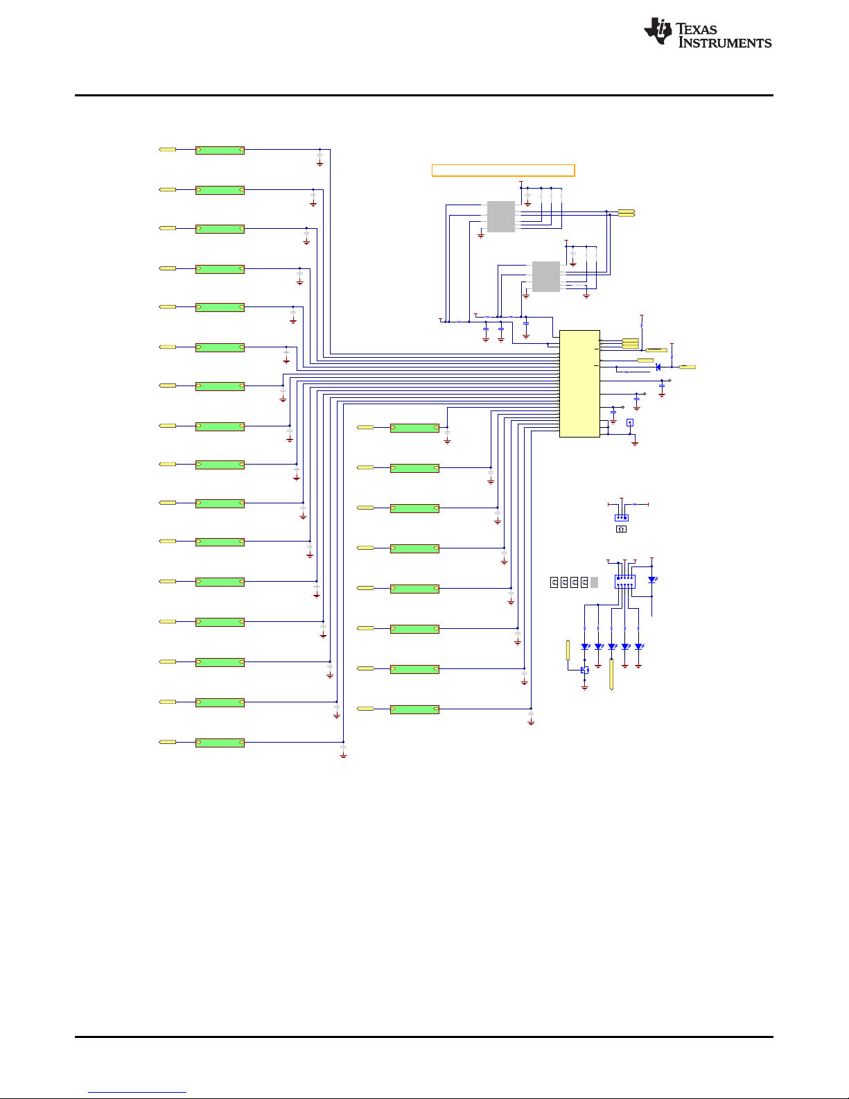
6.1 Main Board Schematic
Figure 13 through Figure 17 illustrate the main board schematics.
Board Files
SCPU036–October 2017
Submit Documentation Feedback
Figure 13. Page Connections
Copyright © 2017, Texas Instruments Incorporated
TIC12400 Evaluation Module
39
Page 40
GND
GND
GND
0.1µF
C32
VDD
1
TP3
GND
SCLK
SI
SO
0.1µF
C31
DPI/CE injection/measurement po int choosethis one
DPI/CE injection/measurement po int
IN8_SB
IN7_SB
IN6_SB
IN5_SB
IN4_SB
IN3_SB
IN2_SB
IN1_SB
IN0_SB
IN5
IN4
IN3
IN0
IN1
IN2
IN21
IN22
IN23
IN6
IN7
IN10
IN11
IN12
IN8
IN13
IN14
IN15
IN16
IN17
IN18
IN19
IN20
IN9_SB
IN9
1µF
C33
SB_IN_ IN_
0
HVL129A_INx.SchDoc
SB_IN_ IN_
1
HVL129A_INx.SchDoc
SB_IN_ IN_
2
HVL129A_INx.SchDoc
SB_IN_ IN_
3
HVL129A_INx.SchDoc
SB_IN_ IN_
4
HVL129A_INx.SchDoc
SB_IN_ IN_
5
HVL129A_INx.SchDoc
SB_IN_ IN_
6
HVL129A_INx.SchDoc
SB_IN_ IN_
7
HVL129A_INx.SchDoc
SB_IN_ IN_
8
HVL129A_INx.SchDoc
SB_IN_ IN_
9
HVL129A_INx.SchDoc
SB_IN_ IN_
10
HVL129A_INx.SchDoc
SB_IN_ IN_
11
HVL129A_INx.SchDoc
SB_IN_ IN_
12
HVL129A_INx.SchDoc
SB_IN_ IN_
13
HVL129A_INx.SchDoc
SB_IN_ IN_
14
HVL129A_INx.SchDoc
SB_IN_ IN_
15
HVL129A_INx.SchDoc
SB_IN_ IN_
23
HVL129A_INx.SchDoc
SB_IN_ IN_
22
HVL129A_INx.SchDoc
SB_IN_ IN_
21
HVL129A_INx.SchDoc
SB_IN_ IN_
20
HVL129A_INx.SchDoc
SB_IN_ IN_
19
HVL129A_INx.SchDoc
SB_IN_ IN_
18
HVL129A_INx.SchDoc
SB_IN_ IN_
17
HVL129A_INx.SchDoc
SB_IN_ IN_
16
HVL129A_INx.SchDoc
IN13
1
IN14
2
IN15
3
IN16
4
IN17
5
IN18
6
IN19
7
IN208DGND
28
IN21
10
IN22
11
IN23
12
RESET
21
SI
17
SCLK
16
CS
15
SO
18
VDD
19
INT
24
CAP_PRE
22
CAP_D
23
CAP_A
20
IN0
13
IN1
14
IN2
25
IN3
26
IN4
27
AGND
9
IN5
29
IN6
30
IN7
31
IN8
32
IN9
33
IN10
34
IN11
35
IN12
36
VS
37
VS
38
EP
39
U11
TIC12400DCPQ1
RESET
GND
VS
SCL
GND
SDA
GND
0.01µF
C59
DNP
GND
0.01µF
C57
DNP
GND
0.01µF
C55
DNP
GND
0.01µF
C53
DNP
GND
0.01µF
C51
DNP
GND
0.01µF
C49
DNP
GND
0.01µF
C47
DNP
GND
0.01µF
C45
DNP
GND
0.01µF
C60
DNP
0.01µF
C58
DNP
GND
0.01µF
C56
DNP
GND
0.01µF
C54
DNP
GND
0.01µF
C52
DNP
GND
0.01µF
C50
DNP
GND
0.01µF
C48
DNP
GND
0.01µF
C46
DNP
GND
0.01µF
C44
DNP
GND
0.01µF
C43
DNP
GND
0.01µF
C42
DNP
GND
0.01µF
C41
DNP
GND
0.01µF
C40
DNP
GND
0.01µF
C39
DNP
GND
0.01µF
C38
DNP
GND
0.01µF
C37
DNP
GND
0.1µF
C30
0.1µF
C29
0.1µF
C36
DNP
0.1µF
C11
DNP
0 R15
4.7µF
C20
GND
/CS
A1
1
A0
2
ALERT
3
SDA
4
SCL
5
VS+
6
GND
7
VBUS
8
VIN-
9
VIN+
10
U12
INA226AIDGSR
DNP
A1
1
A0
2
ALERT
3
SDA
4
SCL
5
VS+
6
GND
7
VBUS
8
VIN-
9
VIN+
10
U13
INA226AIDGSR
DNP
+3.3V
GND
+3.3V
GND
GND
I2C Cur ren t Shun t i s u sed to mea su re curren t for V s and Vdd
4.99k
R9
DNP
4.99k
R11
DNP
4.99k
R16
DNP
4.99k
R17
DNP
4.99k
R18
DNP
4.99k R19
DNP
GND
GND
IN0
IN1
IN2
IN3
IN4
IN5
IN6
IN7
IN8
IN9
IN10
IN11
IN12
IN13
IN14
IN15
IN16
IN17
IN18
IN20
IN21
IN22
IN23
IN19
IndicatorLEDs
+3.3V +5V
Green
1
2
D4
GND
MSP-LED
Green
1
2
D5
GND
Green
1
2
D1
3
5,6,84,7
1,2,
Q1
CSD17313Q2
GND
Red
1
2
D6
Green
1
2
D7
VS
Vssint
Vssint
INT_LED
750
R25
5.10k
R28
750
R27
750
R2
1.62k
R26
/INT
INT_LED
VS
4.32k
R20
VDD
MOSI
CS_MSDI
MISO
SCLK
RST
VDD
10k
R24
Green
1
2
D2
EN_EXT_MICRO
750
R13
INT
D8
BAS 52-02V H6327
VDD
2.00k
R3
0 R31
0 R10
123456789
10
J4
A
D
PRE
123
J12
SH-J12
SH-MSP_LED
SH-3.3V
SH-EXT_MC
SH-5V
SH-INT
DNP
Copyright © 2017, Texas Instruments Incorporated
Board Files
www.ti.com
40
TIC12400 Evaluation Module
Figure 14. Main Device
Copyright © 2017, Texas Instruments Incorporated
SCPU036–October 2017
Submit Documentation Feedback
Page 41

GND
IN_SB_IN_
0.015µF
C1_0
220
R1_0
IN_0
Copyright © 2017, Texas Instruments Incorporated
GND
2.2µF
C23
VDD
0.1µF
C22
GND
GND
VS
47µF
C24
12V Battery Input
TAB
VIN1VOUT
3
4
U9
TPS7A6550QKVURQ1
GND
GND
VBAT_MSDI
GND_MSDI
+3.3V
+5V
0.1µF
C28
J9
SPC15363
J10
SPC15354
600 ohm
L1
+VBUS
0
R14
DNP
Vbat_c TP2
D3
SS34
123
J7
1
2
J1
1
2
J11
SH-J7
SH-J11
SH-J1
DNP
Copyright © 2017, Texas Instruments Incorporated
GND
GND
+3.3V
GND
GND
GND
GND
GND
GND
GND
GND
GND
IO1
1
IO2
2
GND3IO3
4
IO4
5
VCC
6
U3
TPD4E004DRYR
33k
R8
33
R4
33
R6
10µF
C9
1.5k
1.07Meg
R22
220pF
C10
7.5V
2
1
Z2
1SMB5922BT3G
22µF
C13
0.01µF
C15
2.2µF
C12
Alternate Functions for GPIO pins:
-------------------------------------------------------------GPIO0 - I2C:SDA
GPIO1 - I2C:SCL
GPIO2 - SPI:SCLK, EasyScale:DOUT, uWire:SCLK
GPIO3 - PWM2, INT0
GPIO4 - SPI:MOSI, UART:TXD, uWIRE:MOSI
GPIO5 - SPI:MISO, UART:RXD,uWIRE:MISO
GPIO6 - PWM1, OW1, SPI:CS
GPIO7 - PWM0, OW2, INT2
GPIO8 - ADC3
GPIO9 - ADC2, EasyScale:AIN
GPIO10 - VEREFGPIO11 - VEREF+
GPIO12 - FEC, CLOCK, INT3
GPIO13 - PWM3
VUSB
PUR
DP
DM
VBUS
0.1µF
C25
GND
GND
+3.3V
49.9k
R23
GND
+3.3V
EXT_MICRO_CONTROL
A1
1
VCCA
2
A2
3
A3
4
A4
5
A5
6
A6
7
OE
8
GND
9
B6
10
B5
11
B4
12
B3
13
B2
14
VCCB
15
B1
16
U10
TXB0106PWR
0.1µF
C26
GND
VDD
2
3
4
1
5
J5
41
32
S1
1µF
C14
90 ohm
FB1
OUT
1
NR
3
4
EN
5
IN
8
9
GND
U4A
TPS73533DRBR
Place on bottom of board on opposing side of thermal pad
so that thermal resistance is minimiz ed
Place on top of board in secluded section of PCB then hav e
internal pours kept out and machine out slots to ther mally
isolate from board
49.9k
R5
NC
2
NC
6
NC
7
U4B
TPS73533DRBR
CS_MSDI
SCLK
MOSI
MISO
0 R33
0 R34
0 R39
0 R40
INT
0 R41
RST
0 R42
GPIO6
GPIO2
GPIO4
GPIO5
GPIO3
GPIO7
+VBUS
3
5,6,8
4,7
1,2,
Q2
CSD17313Q2
TP1
EN_EXT_MICRO
GPIO12
P6.4/CB4/A4
1
P6.5/CB5/A5
2
P6.6/CB6/A6
3
P6.7/CB7/A7
4
P7.0/CB8/A12
5
P7.1/CB9/A13
6
P7.2/CB10/A14
7
P7.3/CB11/A15
8
P5.0/A8/VREF+/VEREF+
9
P5.1/A9/VREF-/VEREF-
10
AVCC1
11
P5.4/XIN
12
P5.5/XOUT
13
AVSS1
14
P8.0
15
P8.1
16
P8.2
17
DVCC1
18
DVSS1
19
VCORE
20
P1.0/TA0CLK/ACLK
21
P1.1/TA0.0
22
P1.2/TA0.1
23
P1.3/TA0.2
24
P1.4/TA0.3
25
P1.5/TA0.4
26
P1.6/TA1CLK/CBOUT
27
P1.7/TA1.0
28
P2.0/TA1.1
29
P2.1/TA1.2
30
P2.2/TA2CLK/SMCLK
31
P2.3/TA2.0
32
P2.4/TA2.1
33
P2.5/TA2.2
34
P2.6/RTCCLK/DMAE0
35
P2.7/UCB0STE/UCA0CLK
36
P3.0/UCB0SIMO/UCB0SDA
37
P3.1/UCB0SOMI/UCB0SCL
38
P3.2/UCB0CLK/UCA0STE
39
P3.3/UCA0TXD/UCA0SIMO
40
P3.4/UCA0RXD/UCA0SOMI
41
P3.5/TB0.5
42
P3.6/TB0.6
43
P3.7/TB0OUTH/SVMOUT
44
P4.0/PM_UCB1STE/PM_UCA1CLK
45
P4.1/PM_UCB1SIMO/PM_UCB1SDA
46
P4.2/PM_UCB1SOMI/PM_UCB1SCL
47
P4.3/PM_UCB1CLK/PM_UCA1STE
48
DVSS2
49
DVCC2
50
P4.4/PM_UCA1TXD/PM_UCA1SIMO
51
P4.5/PM_UCA1RXD/PM_UCA1SOMI
52
P4.6/PM_NONE
53
P4.7/PM_NONE
54
P5.6/TB0.0
55
P5.7/TB0.1
56
P7.4/TB0.2
57
P7.5/TB0.3
58
P7.6/TB0.4
59
P7.7/TB0CLK/MCLK
60
VSSU
61
PU.0/DP
62
PUR
63
PU.1/DM
64
VBUS
65
VUSB
66
V18
67
AVSS2
68
P5.2/XT2IN
69
P5.3/XT2OUT
70
TEST/SBWTCK
71
PJ.0/TDO
72
PJ.1/TDI/TCLK
73
PJ.2/TMS
74
PJ.3/TCK
75
RST/NMI/SBWTDIO
76
P6.0/CB0/A0
77
P6.1/CB1/A1
78
P6.2/CB2/A2
79
P6.3/CB3/A3
80
U1
MSP430F5529IPNR
MINI-USB
GPIO9
GPIO8
GPIO11
GPIO10
P8.0
GPIO12
GPIO7
SDA
SDABRD
SCLBRD
SCL
I2CPU
GPIO0SDABRD
GPIO1SCLBRD
GPIO4
GPIO2
GPIO6
GPIO3
GPIO5
MSP-LED
GPIO13
GND
0.1µF
C6
GND
0.1µF
C5
DP
PUR
DM
VBUS
VUSB
V18
GND
1 2
24MHz
Y1
+3.3V
2200pF
C3
GND
33k
R12
GND
1 2
3 4
5 6
7 8
9 10
11 12
13 14
J8
DNP
JTAG
30pF
C2
30pF
C34
GND
GND
0.47µF
C7
220pF
C16
GND
+3.3V
GND
JTAG8
JTAG8
SCL
1
GND
2
ALERT
3
ADD0
4
V+
5
SDA
6
U5
TMP102AQDRLRQ1
DNP0.1µF
C18
DNP
GND
4.99k R32
DNP
+3.3V
+3.3V
SDABRD
SCLBRD
GND
+3.3V
SCL
1
GND
2
ALERT
3
ADD0
4
V+
5
SDA
6
U2
TMP102AQDRLRQ1
DNP
GND
0.1µF
C8
DNP
GND
4.99k R35
DNP
4.99k R37
DNP
+3.3V
+3.3V
4.99k R36
DNP
SDABRD
SCLBRD
0.1µF
C4
123
J6
1
2
JP1
SH-J6
SH-J2
DNP
Copyright © 2017, Texas Instruments Incorporated
www.ti.com
Board Files
SCPU036–October 2017
Submit Documentation Feedback
Figure 17. Input filters – IN10-IN23 use 10 Ω instead of 220 Ω
Figure 15. USB interface
Figure 16. <Caption>
Copyright © 2017, Texas Instruments Incorporated
TIC12400 Evaluation Module
41
Page 42

1
J4
1
J5
J8
J9
1234567
8
SW23_B
123456789
101112
SW18
IN0
IN1
IN2
IN3
IN4
IN10
IN11
IN12
IN13
IN14
IN16
IN17
IN15
IN18
IN19
IN20
IN22
IN23
IN21
123456789
101112
SW19
123456789
101112
SW20
123456789
101112
SW21
123456789
101112
SW22
123456789
101112
SW23_A
VBAT
VBAT
VBAT
VBAT
VBAT
VBAT
CGNDGND
CGND
GND
IN5
IN6
IN7
IN8
IN9
A1
A2
A3
A4
A5
A6
A7
A8
A9
A10
A11
A12
A13
A14
A15
A16
B1
B2
B3
B4
B5
B6
B7
B8
B9
B10
B11
B12
B13
B14
B15
B16
C1
C2
C3
C4
C5
C6
C7
C8
C9
C10
C11
C12
C13
C14
C15
C16
J7
IN1_SB
IN22_SB
IN0_SB
IN19_SB
IN16_SB
IN12_SB
IN9_SB
IN6_SB
IN2_SB
IN23_SB
IN21_SB
IN20_SB
IN18_SB
IN17_SB
IN15_SB
IN14_SB
IN13_SB
IN11_SB
IN8_SB
IN10_SB
IN7_SB
IN5_SB
IN3_SB
IN4_SB
IN0_SB
IN1_SB
IN2_SB
IN3_SB
IN4_SB
IN5_SB
IN6_SB
IN7_SB
IN8_SB
IN9_SB
IN10_SB
IN11_SB
IN12_SB
IN13_SB
IN14_SB
IN15_SB
IN16_SB
IN17_SB
IN18_SB
IN19_SB
IN20_SB
IN21_SB
IN22_SB
IN23_SB
100
R37
100
R40
100
R43
100
R46
100
R49
100
R52
100R36
100R34
100R32
100R30
470R21
470R23
470R25
470R27
294
R38
294
R41
294
R44
294
R47
294
R50
402
R54
887
R55
1.65k
R56
220
R53
23-523-1 23-423-2 23-322-1 2 2-2 22-321-1 21-2 21-320-1 20-2 20-319-1 19-2 19-318-1 18-2 18-3
750
R51
750
R48
750
R45
750
R42
750
R39
VBAT
VBAT
OPEN
SW11-1
SW11-2
OPEN
SW1-1
SW1-2
OPEN
SW2-1
SW2-2
OPEN
SW3-1
SW3-2
OPEN
SW4-1
SW4-2
OPEN
SW5-1
SW5-2
OPEN
SW6-1
SW6-2
OPEN
SW7-1
SW7-2
OPEN
SW8-1
SW8-2
OPEN
SW9-1
SW9-2
OPEN
SW10-1
SW10-2
OPEN
SW12-1
SW12-2
OPEN
SW13-1
SW13-2
OPEN
SW14-1
SW14-2
OPEN
SW15-1
SW15-2
OPEN
SW16-1
SW16-2
OPEN
SW17-1
SW17-2
VBAT
CGND CGND CGND CGND CGND CG ND CGND
0
R19
0
R17
0
R15
0
R13
0
R11
0
R9
0
R7
0
R3
0
R2
0
R4
0
R6
0
R8
0
R10
0
R12
0
R14
0
R18
0
R20
VBAT
CGND
2
1
3
4
S1S1S2
S2
SW0
CGND CGND
VBAT
0
R1
OPEN
SW0-1
SW0-2
2
1
3
4
S1S1S2
S2
SW1
2
1
3
4
S1S1S2
S2
SW2
2
1
3
4
S1S1S2
S2
SW3
2
1
3
4
S1S1S2
S2
SW4
CGNDCGND
CGNDCGND
CGNDCGND
CGNDCGND
VBAT
0
R5
2
1
3
4
S1S1S2
S2
SW5
CGND CGND
2
1
3
4
S1S1S2
S2
SW6
2
1
3
4
S1S1S2
S2
SW7
2
1
3
4
S1S1S2
S2
SW8
2
1
3
4
S1S1S2
S2
SW9
CGNDCGND
CGNDCGND
CGNDCGND
CGNDCGND
0
R16
2
1
3
4
S1S1S2
S2
SW10
CGND CGND
2
1
3
4
S1S1S2
S2
SW11
2
1
3
4
S1S1S2
S2
SW12
2
1
3
4
S1S1S2
S2
SW13
2
1
3
4
S1S1S2
S2
SW14
2
1
3
4
S1S1S2
S2
SW15
2
1
3
4
S1S1S2
S2
SW16
2
1
3
4
S1S1S2
S2
SW17
CGND
CGND CGND
CGND
CGND CGND
CGND
CGND CGND
CGND
CGND CGND
CGND
CGND CGND
CGND
CGND CGND
CGND
CGND CGND
CGND
100R22
100R24
100R26
100R28
470R29
470R35
470R33
470R31
1
2
J6
1 2
3 4
5 6
7 8
9 10
11 12
13 14
15
17
19
16
18
20
J1
1 2
3 4
5 6
7 8
9 10
11 12
13 14
15 16
J2
1 2
3 4
5 6
7 8
9 10
11 12
J3
SH-0
SH-1
SH-2
SH-3
SH-4
SH-5
SH-6
SH-7
SH-8
SH-9
SH-18
SH-19
SH-20
SH-21
SH-22
SH-23
SH-11
SH-12
SH-13
SH-14
SH-15
SH-16
SH-17
SH-10
SH-J6
Copyright © 2017, Texas Instruments Incorporated
Board Files
6.2 Switch Board Schematic
Figure 18 shows the SWITCH board schematic.
42
TIC12400 Evaluation Module
Figure 18. SWITCH Board Schematic
Copyright © 2017, Texas Instruments Incorporated
www.ti.com
SCPU036–October 2017
Submit Documentation Feedback
Page 43

www.ti.com
Board Files
43
SCPU036– October 2017
Submit Documentation Feedback
Copyright © 2017, Texas Instruments Incorporated
TIC12400 Evaluation Module
6.3 Main Board Bill of Materials
Table 1 lists the main board bill of materials (BOM).
Table 1. Main Board Bill of Materials
Designator QTY Value Description Package Reference Part Number
!PCB1 1 Printed Circuit Board HVL129
!PCB2 1 Daughter card load board. Set in separate ESD bag. Kiting item. N/A HVL149
C1_0, C1_1, C1_2,
C1_3, C1_4, C1_5,
C1_6, C1_7, C1_8,
C1_9, C1_10, C1_11,
C1_12, C1_13,
C1_14, C1_15,
C1_16, C1_17,
C1_18, C1_19,
C1_20, C1_21,
C1_22, C1_23
24 0.015uF CAP, CERM, 0.015 µF, 100 V, +/- 10%, X7R, 0603 0603 C0603C153K1RACTU
C2, C34 2 30pF CAP, CERM, 30pF, 100V, +/-5%, C0G/NP0, 0603 0603 GRM1885C2A300JA01D
C3 1 2200pF CAP, CERM, 2200pF, 50V, +/-10%, X7R, 0603 0603 C0603X222K5RACTU
C4, C5, C6 3 0.1uF CAP, CERM, 0.1uF, 16V, +/-5%, X7R, 0603 0603 0603YC104JAT2A
C7 1 0.47uF CAP, CERM, 0.47uF, 10V, +/-10%, X7R, 0603 0603 C0603C474K8RACTU
C9 1 10uF CAP, CERM, 10uF, 16V, +/-20%, X5R, 0805 0805 0805YD106MAT2A
C10, C16 2 220pF CAP, CERM, 220pF, 50V, +/-1%, C0G/NP0, 0603 0603 06035A221FAT2A
C12 1 2.2uF CAP, CERM, 2.2uF, 16V, +/-10%, X5R, 0805 0805 0805YD225KAT2A
C13 1 22uF CAP ALUM 22UF 10V 20% SMD E55 EEE-1AA220WR
C14 1 1uF CAP, CERM, 1 µF, 25 V, +/- 10%, X7R, 0805 0805 C0805C105K3RACTU
C15 1 0.01uF CAP, CERM, 0.01uF, 50V, +/-10%, X7R, 0603 0603 C1608X7R1H103K
C20 1 4.7uF CAP, CERM, 4.7 µF, 50 V, +/- 20%, X7R, 1206_190 1206_190 C3216X7R1H475M160AC
C22, C31, C32 3 0.1uF CAP,CERM, 0.1 µF, 25 V, +/- 5%, X7R, 0603 0603 C0603C104J3RAC
C23 1 2.2uF CAP, CERM, 2.2 µF, 10 V, +/- 10%, X7R, 0805 0805 GRM21BR71A225KA01L
C24 1 47uF CAP, AL, 47 µF, 63 V, +/- 20%, ohm, SMD SMT Radial G EEETG1J470P
C25, C26 2 0.1uF CAP, CERM, 0.1 µF, 25 V, +/- 5%, X7R, 0603 0603 C0603C104J3RACTU
C28 1 0.1uF CAP, CERM, 0.1 µF, 50 V, +/- 10%, X7R, 0805 0805 C0805C104K5RACTU
C29, C30 2 0.1uF CAP, CERM, 0.1 µF, 50 V, +/- 10%, X7R, 0603 0603 06035C104KAT2A
C33 1 1uF CAP, CERM, 1 µF, 50 V, +/- 10%, X7R, 0603 0603 UMK107AB7105KA-T
D1, D2, D4, D5, D7 5 Green LED, Green, SMD 1.6x0.8x0.8mm LTST-C190KGKT
D3 1 40V Diode, Schottky, 40 V, 3 A, SMC SMC SS34
D6 1 Red LED, Red, SMD LED_0603 LTST-C191KRKT
D8 1 45V Diode, Schottky, 45 V, 0.75 A, SOD-523 SOD-523 BAS 52-02V H6327
FB1 1 90 ohm Ferrite Bead, 90 ohm @ 100 MHz, 1.5 A, 1206 1206 MI1206K900R-10
H2, H5, H8, H11 4 Standoff, Hex, 1"L #4-40 Nylon Standoff 1902E
H3, H6, H9, H12 4 Machine Screw, Round, #4-40 x 1/4, Nylon, Philips panhead Screw NY PMS 440 0025 PH
Page 44

Board Files
www.ti.com
44
SCPU036– October 2017
Submit Documentation Feedback
Copyright © 2017, Texas Instruments Incorporated
TIC12400 Evaluation Module
Table 1. Main Board Bill of Materials (continued)
Designator QTY Value Description Package Reference Part Number
IN_0, IN_1, IN_2,
IN_3, IN_4, IN_5,
IN_6, IN_7, IN_8,
IN_9, IN_10, IN_11,
IN_12, IN_13, IN_14,
IN_15, IN_16, IN_17,
IN_18, IN_19, IN_20,
IN_21, IN_22, IN_23
24 Test Lead clips and hooks, SMT Test Point, Body 3.25x1.65mm S1751-46
J1, J11, JP1 3 Header, 100mil, 2x1, Gold with Tin Tail, SMT 2x1 Header TSM-102-01-L-SV
J2 1 Header, 2.54mml, 16x3, Gold, TH Header, 2.54mml, 16x3, TH 5650478-5
J4 1 Header, 2.54mm, 5x2, Gold, SMT Header, 2.54mm, 5x2, SMT TSM-105-01-L-DV-P
J5 1 Connector, Receptacle, Mini-USB Type B, R/A, Top Mount SMT USB Mini Type B 1734035-2
J6, J7, J12 3 Header, 100mil, 3x1, Gold, SMT Samtec_TSM-103-01-X-SV TSM-103-01-L-SV
J9 1 BANANA JACK, SOLDER LUG, RED, TH Red Insulated Banana Jack SPC15363
J10 1 BANANA JACK, SOLDER LUG, BLACK, TH Black Insulated Banana Jack SPC15354
L1 1 600 ohm Ferrite Bead, 600 ohm @ 100 MHz, 2 A, 0805 0805 MPZ2012S601A
Q1, Q2 2 30V MOSFET, N-CH, 30 V, 5 A, SON 2x2mm SON 2x2mm CSD17313Q2
R1_0, R1_1, R1_2,
R1_3, R1_4, R1_5,
R1_6, R1_7, R1_8,
R1_9
10 220 RES, 220, 1%, 0.5 W, AEC-Q200 Grade 0, 0805 0805 ERJ-P6WF2200V
R1_10, R1_11,
R1_12, R1_13,
R1_14, R1_15,
R1_16, R1_17,
R1_18, R1_19,
R1_20, R1_21,
R1_22, R1_23
14 10.0 RES, 10.0, 1%, 0.5 W, AEC-Q200 Grade 0, 0805 0805 ERJ-P6WF10R0V
R2, R13, R25, R27 4 750 RES, 750, 5%, 0.1 W, 0603 0603 CRCW0603750RJNEA
R3 1 2.00k RES, 2.00 k, 1%, 0.1 W, 0603 0603 CRCW06032K00FKEA
R4, R6 2 33 RES, 33 ohm, 5%, 0.063W, 0402 0402 CRCW040233R0JNED
R5, R23 2 49.9k RES, 49.9 k, 1%, 0.1 W, 0603 0603 CRCW060349K9FKEA
R7 1 1.5k RES, 1.5k ohm, 5%, 0.063W, 0402 0402 CRCW04021K50JNED
R8, R12 2 33k RES, 33k ohm, 5%, 0.063W, 0402 0402 CRCW040233K0JNED
R10, R15, R31, R33,
R34, R39, R40, R41,
R42
9 0 RES, 0, 5%, 0.1 W, 0603 0603 CRCW06030000Z0EA
R20 1 4.32k RES, 4.32 k, 1%, 0.1 W, 0603 0603 RC0603FR-074K32L
R22 1 1.07Meg RES, 1.07Meg ohm, 1%, 0.1W, 0603 0603 CRCW06031M07FKEA
R24 1 10k RES, 10 k, 5%, 0.1 W, 0603 0603 CRCW060310K0JNEA
R26 1 1.62k RES, 1.62 k, 1%, 0.1 W, 0603 0603 CRCW06031K62FKEA
R28 1 5.10k RES, 5.10 k, 1%, 0.1 W, 0603 0603 RC0603FR-075K1L
S1 1 Switch, Tactile, SPST-NO, SMT Switch, 6.1x1.8x4.6 mm EVQ-PSD02K
Page 45

www.ti.com
Board Files
45
SCPU036– October 2017
Submit Documentation Feedback
Copyright © 2017, Texas Instruments Incorporated
TIC12400 Evaluation Module
Table 1. Main Board Bill of Materials (continued)
Designator QTY Value Description Package Reference Part Number
SH-3.3V, SH-5V, SHEXT_MC, SH-J6, SHJ7, SH-J11, SH-J12,
SH-MSP_LED
8 1x2 Shunt, 100mil, Gold plated, Black Shunt SNT-100-BK-G
TP1 1 Test Point, Multipurpose, Black, TH Black Multipurpose Testpoint 5011
TP2 1 Test Point, Multipurpose, Red, TH Red Multipurpose Testpoint 5010
TP3 1 Header, 100mil, 1pos, Gold, TH Testpoint TSW-101-07-G-S
TP4 1 Header, 2.54mm, 24x1, Gold, TH Header, 2.54mm, 24x1, TH PEC24SAAN
U1 1 25 MHz Mixed Signal Microcontroller with 128 KB Flash, 8192 B SRAM and 63 GPIOs, -40 to 85
degC, 80-pin QFP (PN), Green (RoHS & no Sb/Br)
PN0080A MSP430F5529IPNR
U3 1 TPD4E0
04DRYR
IC, 4-Chan ESD-Protection Array SON-6 TPD4E004DRYR
U4 1 Single Output High PSRR LDO, 500 mA, Fixed 3.3 V Output, 2.7 to 6.5 V Input, with Low IQ, 8-
pin SON (DRB), -40 to 125 degC, Green (RoHS & no Sb/Br)
DRB0008A TPS73533DRBR
U9 1 Single Output Automotive LDO, 300 mA, Fixed 5 V Output, 4 to 40 V Input, 3-pin PFM (KVU),
-40 to 125 degC, Green (RoHS & no Sb/Br)
KVU0003A TPS7A6550QKVURQ1
U10 1 6-BIT BIDIRECTIONAL VOLTAGE-LEVEL TRANSLATOR WITH AUTO-DIRECTION SENSING
AND ±15-kV ESD PROTECTION, PW0016A
PW0016A TXB0106PWR
U11 1 Multiple Switch Detection Interface (MSDI) device, DCP0038A DCP0038A TIC12400DCPQ1
Y1 1 Crystal, 24.000MHz, 20pF, SMD Crystal, 11.4x4.3x3.8mm ECS-240-20-5PX-TR
Z2 1 7.5V Diode, Zener, 7.5V, 550mW, SMB SMB 1SMB5922BT3G
C8, C18 0 0.1uF CAP, CERM, 0.1 µF, 25 V, +/- 5%, X7R, 0603 0603 C0603C104J3RACTU
C11, C36 0 0.1uF CAP, CERM, 0.1 µF, 50 V, +/- 10%, X7R, 0603 0603 06035C104KAT2A
C37, C38, C39, C40,
C41, C42, C43, C44,
C45, C46, C47, C48,
C49, C50, C51, C52,
C53, C54, C55, C56,
C57, C58, C59, C60
0 0.01uF CAP, CERM, 0.01 µF, 50 V, +/- 5%, X7R, 0603 0603 C0603C103J5RACTU
FID1, FID2, FID3 0 Fiducial mark. There is nothing to buy or mount. N/A N/A
J3 0 Header(Shrouded), 2.54mm, 5x2, Gold, TH Header, 2.54mm, 5x2, TH AWHW-10G-0202-T
J8 0 Header, 100mil, 7x2, SMT Header, 100 mil, 7x2, SMT 0015912140
R9, R11, R16, R17,
R18, R19, R32, R35,
R36, R37
0 4.99k RES, 4.99 k, 1%, 0.1 W, 0603 0603 CR0603-FX-4991ELF
R14 0 0 RES, 0, 5%, 0.1 W, 0603 0603 CRCW06030000Z0EA
SH-INT, SH-J1, SH-J20 1x2 Shunt, 100mil, Gold plated, Black Shunt SNT-100-BK-G
U2, U5 0 Low-Power Digital Temperature Sensor With SMBus and Two-Wire Serial Interface in SOT563,
DRL0006A
DRL0006A TMP102AQDRLRQ1
U12, U13 0 High-or Low-Side Measurement, Bi-Directional CURRENT/POWER MONITOR with I2C(TM)
Interface, DGS0010A
DGS0010A INA226AIDGSR
Page 46

Board Files
www.ti.com
46
SCPU036– October 2017
Submit Documentation Feedback
Copyright © 2017, Texas Instruments Incorporated
TIC12400 Evaluation Module
6.4 SWITCH Board Bill of Materials
Table 2 lists the SWITCH board BOM.
Table 2. SWITCH Board Bill of Materials
Designator QTYValue Description Package Reference Part Number
!PCB1 1 Printed Circuit Board HVL149
H1, H2, H3, H4 4 Machine Screw, Round, #4-40 x 1/4, Nylon, Philips panhead Screw NY PMS 440 0025 PH
H5, H6, H7, H8 4 Standoff, Hex, 1"L #4-40 Nylon Standoff 1902E
J1 1 Header, 2.54mm, 10x2, Gold, SMT 1000x180x290mil TSM-110-01-L-DV-P
J2 1 Header, 2.54mm, 8x2, Gold, SMT Header, 2.54mm, 8x2, SMT TSM-108-01-L-DV
J3 1 Header, 2.54mm, 6x2, Gold, SMT Header, 2.54mm, 6x2, SMT TSM-106-01-L-DV
J4, J5 2 Header, 100mil, 1pos, Gold, TH Testpoint TSW-101-07-G-S
J6 1 Header, 2.54 mm, 2x1, Gold, R/A, SMT Header, 2.54 mm, 2x1, R/A,
SMT
0878980204
J7 1 Receptacle, 2.54mm, 16x3, Gold, R/A, TH Receptacle,2.54mm, 16x3, R/A,TH5650868-4
J8 1 BANANA JACK, SOLDER LUG, RED, TH Red Insulated Banana Jack SPC15363
J9 1 BANANA JACK, SOLDER LUG, BLACK, TH Black Insulated Banana Jack SPC15354
R1, R2, R3, R4, R5,
R6, R7, R8, R9, R10,
R11, R12, R13, R14,
R15, R16, R17, R18,
R19, R20
20 0 RES, 0, 5%, 0.25 W, 1206 1206 ERJ-8GEY0R00V
R21, R23, R25, R27,
R29, R31, R33, R35
8 470 RES, 470, 1%, 0.25 W, 1206 RC1206FR-07470RL
R22, R24, R26, R28,
R30, R32, R34, R36
8 100 RES, 100, 1%, 0.25 W, 1206 ERJ-8ENF1000V
R37, R40, R43, R46,
R49, R52
6 100 RES, 100, 1%, 0.25 W, 1206 1206 ERJ-8ENF1000V
R38, R41, R44, R47,
R50
5 294 RES, 294, 1%, 0.25 W, 1206 1206 RC1206FR-07294RL
R39, R42, R45, R48,
R51
5 750 RES, 750, 1%, 0.25 W, 1206 1206 CRCW1206750RFKEA
R53 1 220 RES, 220, 1%, 0.25 W, 1206 1206 RC1206FR-07220RL
R54 1 402 RES, 402, 1%, 0.25 W, 1206 1206 ERJ-8ENF4020V
R55 1 887 RES, 887, 1%, 0.25 W, 1206 1206 ERJ-8ENF8870V
R56 1 1.65k RES, 1.65 k, 1%, 0.25 W, 1206 1206 ERJ-8ENF1651V
Page 47

www.ti.com
Board Files
47
SCPU036– October 2017
Submit Documentation Feedback
Copyright © 2017, Texas Instruments Incorporated
TIC12400 Evaluation Module
Table 2. SWITCH Board Bill of Materials (continued)
Designator QTYValue Description Package Reference Part Number
SH-0, SH-1, SH-2,
SH-3, SH-4, SH-5,
SH-6, SH-7, SH-8,
SH-9, SH-10, SH-11,
SH-12, SH-13, SH14, SH-15, SH-16,
SH-17, SH-18, SH19, SH-20, SH-21,
SH-22, SH-23, SH-J6
25 1x2 Shunt, 100mil, Gold plated, Black Shunt SNT-100-BK-G
SW0, SW1, SW2,
SW3, SW4, SW5,
SW6, SW7, SW8,
SW9, SW10, SW11,
SW12, SW13, SW14,
SW15, SW16, SW17
18 Switch, Slide, SP3T, On-On-On, 3 Pos, 0.3A, 30 VDC, TH 12.6x4.3mm SS-13D16-VG 4 PA
SW18, SW19, SW20,
SW21, SW22,
SW23_A
6 Switch, DPST, 3 Pos, 0.1 A, 50 VDC, SMD 17.67x9.78mm 204-213ST
SW23_B 1 Switch, DPST, 2 Pos, 0.1 A, 50 VDC, SMD 12.34x9.78mm 204-212ST
FID1, FID2, FID3 0 Fiducial mark. There is nothing to buy or mount. N/A N/A
Page 48

STANDARD TERMS FOR EVALUATION MODULES
1. Delivery: TI delivers TI evaluation boards, kits, or modules, including any accompanying demonstration software, components, and/or
documentation which may be provided together or separately (collectively, an “EVM” or “EVMs”) to the User (“User”) in accordance
with the terms set forth herein. User's acceptance of the EVM is expressly subject to the following terms.
1.1 EVMs are intended solely for product or software developers for use in a research and development setting to facilitate feasibility
evaluation, experimentation, or scientific analysis of TI semiconductors products. EVMs have no direct function and are not
finished products. EVMs shall not be directly or indirectly assembled as a part or subassembly in any finished product. For
clarification, any software or software tools provided with the EVM (“Software”) shall not be subject to the terms and conditions
set forth herein but rather shall be subject to the applicable terms that accompany such Software
1.2 EVMs are not intended for consumer or household use. EVMs may not be sold, sublicensed, leased, rented, loaned, assigned,
or otherwise distributed for commercial purposes by Users, in whole or in part, or used in any finished product or production
system.
2 Limited Warranty and Related Remedies/Disclaimers:
2.1 These terms do not apply to Software. The warranty, if any, for Software is covered in the applicable Software License
Agreement.
2.2 TI warrants that the TI EVM will conform to TI's published specifications for ninety (90) days after the date TI delivers such EVM
to User. Notwithstanding the foregoing, TI shall not be liable for a nonconforming EVM if (a) the nonconformity was caused by
neglect, misuse or mistreatment by an entity other than TI, including improper installation or testing, or for any EVMs that have
been altered or modified in any way by an entity other than TI, (b) the nonconformity resulted from User's design, specifications
or instructions for such EVMs or improper system design, or (c) User has not paid on time. Testing and other quality control
techniques are used to the extent TI deems necessary. TI does not test all parameters of each EVM.
User's claims against TI under this Section 2 are void if User fails to notify TI of any apparent defects in the EVMs within ten (10)
business days after delivery, or of any hidden defects with ten (10) business days after the defect has been detected.
2.3 TI's sole liability shall be at its option to repair or replace EVMs that fail to conform to the warranty set forth above, or credit
User's account for such EVM. TI's liability under this warranty shall be limited to EVMs that are returned during the warranty
period to the address designated by TI and that are determined by TI not to conform to such warranty. If TI elects to repair or
replace such EVM, TI shall have a reasonable time to repair such EVM or provide replacements. Repaired EVMs shall be
warranted for the remainder of the original warranty period. Replaced EVMs shall be warranted for a new full ninety (90) day
warranty period.
3 Regulatory Notices:
3.1 United States
3.1.1 Notice applicable to EVMs not FCC-Approved:
FCC NOTICE: This kit is designed to allow product developers to evaluate electronic components, circuitry, or software
associated with the kit to determine whether to incorporate such items in a finished product and software developers to write
software applications for use with the end product. This kit is not a finished product and when assembled may not be resold or
otherwise marketed unless all required FCC equipment authorizations are first obtained. Operation is subject to the condition
that this product not cause harmful interference to licensed radio stations and that this product accept harmful interference.
Unless the assembled kit is designed to operate under part 15, part 18 or part 95 of this chapter, the operator of the kit must
operate under the authority of an FCC license holder or must secure an experimental authorization under part 5 of this chapter.
3.1.2 For EVMs annotated as FCC – FEDERAL COMMUNICATIONS COMMISSION Part 15 Compliant:
CAUTION
This device complies with part 15 of the FCC Rules. Operation is subject to the following two conditions: (1) This device may not
cause harmful interference, and (2) this device must accept any interference received, including interference that may cause
undesired operation.
Changes or modifications not expressly approved by the party responsible for compliance could void the user's authority to
operate the equipment.
FCC Interference Statement for Class A EVM devices
NOTE: This equipment has been tested and found to comply with the limits for a Class A digital device, pursuant to part 15 of
the FCC Rules. These limits are designed to provide reasonable protection against harmful interference when the equipment is
operated in a commercial environment. This equipment generates, uses, and can radiate radio frequency energy and, if not
installed and used in accordance with the instruction manual, may cause harmful interference to radio communications.
Operation of this equipment in a residential area is likely to cause harmful interference in which case the user will be required to
correct the interference at his own expense.
Page 49

FCC Interference Statement for Class B EVM devices
NOTE: This equipment has been tested and found to comply with the limits for a Class B digital device, pursuant to part 15 of
the FCC Rules. These limits are designed to provide reasonable protection against harmful interference in a residential
installation. This equipment generates, uses and can radiate radio frequency energy and, if not installed and used in accordance
with the instructions, may cause harmful interference to radio communications. However, there is no guarantee that interference
will not occur in a particular installation. If this equipment does cause harmful interference to radio or television reception, which
can be determined by turning the equipment off and on, the user is encouraged to try to correct the interference by one or more
of the following measures:
• Reorient or relocate the receiving antenna.
• Increase the separation between the equipment and receiver.
• Connect the equipment into an outlet on a circuit different from that to which the receiver is connected.
• Consult the dealer or an experienced radio/TV technician for help.
3.2 Canada
3.2.1 For EVMs issued with an Industry Canada Certificate of Conformance to RSS-210 or RSS-247
Concerning EVMs Including Radio Transmitters:
This device complies with Industry Canada license-exempt RSSs. Operation is subject to the following two conditions:
(1) this device may not cause interference, and (2) this device must accept any interference, including interference that may
cause undesired operation of the device.
Concernant les EVMs avec appareils radio:
Le présent appareil est conforme aux CNR d'Industrie Canada applicables aux appareils radio exempts de licence. L'exploitation
est autorisée aux deux conditions suivantes: (1) l'appareil ne doit pas produire de brouillage, et (2) l'utilisateur de l'appareil doit
accepter tout brouillage radioélectrique subi, même si le brouillage est susceptible d'en compromettre le fonctionnement.
Concerning EVMs Including Detachable Antennas:
Under Industry Canada regulations, this radio transmitter may only operate using an antenna of a type and maximum (or lesser)
gain approved for the transmitter by Industry Canada. To reduce potential radio interference to other users, the antenna type
and its gain should be so chosen that the equivalent isotropically radiated power (e.i.r.p.) is not more than that necessary for
successful communication. This radio transmitter has been approved by Industry Canada to operate with the antenna types
listed in the user guide with the maximum permissible gain and required antenna impedance for each antenna type indicated.
Antenna types not included in this list, having a gain greater than the maximum gain indicated for that type, are strictly prohibited
for use with this device.
Concernant les EVMs avec antennes détachables
Conformément à la réglementation d'Industrie Canada, le présent émetteur radio peut fonctionner avec une antenne d'un type et
d'un gain maximal (ou inférieur) approuvé pour l'émetteur par Industrie Canada. Dans le but de réduire les risques de brouillage
radioélectrique à l'intention des autres utilisateurs, il faut choisir le type d'antenne et son gain de sorte que la puissance isotrope
rayonnée équivalente (p.i.r.e.) ne dépasse pas l'intensité nécessaire à l'établissement d'une communication satisfaisante. Le
présent émetteur radio a été approuvé par Industrie Canada pour fonctionner avec les types d'antenne énumérés dans le
manuel d’usage et ayant un gain admissible maximal et l'impédance requise pour chaque type d'antenne. Les types d'antenne
non inclus dans cette liste, ou dont le gain est supérieur au gain maximal indiqué, sont strictement interdits pour l'exploitation de
l'émetteur
3.3 Japan
3.3.1 Notice for EVMs delivered in Japan: Please see http://www.tij.co.jp/lsds/ti_ja/general/eStore/notice_01.page 日本国内に
輸入される評価用キット、ボードについては、次のところをご覧ください。
http://www.tij.co.jp/lsds/ti_ja/general/eStore/notice_01.page
3.3.2 Notice for Users of EVMs Considered “Radio Frequency Products” in Japan: EVMs entering Japan may not be certified
by TI as conforming to Technical Regulations of Radio Law of Japan.
If User uses EVMs in Japan, not certified to Technical Regulations of Radio Law of Japan, User is required to follow the
instructions set forth by Radio Law of Japan, which includes, but is not limited to, the instructions below with respect to EVMs
(which for the avoidance of doubt are stated strictly for convenience and should be verified by User):
1. Use EVMs in a shielded room or any other test facility as defined in the notification #173 issued by Ministry of Internal
Affairs and Communications on March 28, 2006, based on Sub-section 1.1 of Article 6 of the Ministry’s Rule for
Enforcement of Radio Law of Japan,
2. Use EVMs only after User obtains the license of Test Radio Station as provided in Radio Law of Japan with respect to
EVMs, or
3. Use of EVMs only after User obtains the Technical Regulations Conformity Certification as provided in Radio Law of Japan
with respect to EVMs. Also, do not transfer EVMs, unless User gives the same notice above to the transferee. Please note
that if User does not follow the instructions above, User will be subject to penalties of Radio Law of Japan.
Page 50

【無線電波を送信する製品の開発キットをお使いになる際の注意事項】 開発キットの中には技術基準適合証明を受けて
いないものがあります。 技術適合証明を受けていないもののご使用に際しては、電波法遵守のため、以下のいずれかの
措置を取っていただく必要がありますのでご注意ください。
1. 電波法施行規則第6条第1項第1号に基づく平成18年3月28日総務省告示第173号で定められた電波暗室等の試験設備でご使用
いただく。
2. 実験局の免許を取得後ご使用いただく。
3. 技術基準適合証明を取得後ご使用いただく。
なお、本製品は、上記の「ご使用にあたっての注意」を譲渡先、移転先に通知しない限り、譲渡、移転できないものとします。
上記を遵守頂けない場合は、電波法の罰則が適用される可能性があることをご留意ください。 日本テキサス・イ
ンスツルメンツ株式会社
東京都新宿区西新宿6丁目24番1号
西新宿三井ビル
3.3.3 Notice for EVMs for Power Line Communication: Please see http://www.tij.co.jp/lsds/ti_ja/general/eStore/notice_02.page
電力線搬送波通信についての開発キットをお使いになる際の注意事項については、次のところをご覧ください。http:/
/www.tij.co.jp/lsds/ti_ja/general/eStore/notice_02.page
3.4 European Union
3.4.1 For EVMs subject to EU Directive 2014/30/EU (Electromagnetic Compatibility Directive):
This is a class A product intended for use in environments other than domestic environments that are connected to a
low-voltage power-supply network that supplies buildings used for domestic purposes. In a domestic environment this
product may cause radio interference in which case the user may be required to take adequate measures.
4 EVM Use Restrictions and Warnings:
4.1 EVMS ARE NOT FOR USE IN FUNCTIONAL SAFETY AND/OR SAFETY CRITICAL EVALUATIONS, INCLUDING BUT NOT
LIMITED TO EVALUATIONS OF LIFE SUPPORT APPLICATIONS.
4.2 User must read and apply the user guide and other available documentation provided by TI regarding the EVM prior to handling
or using the EVM, including without limitation any warning or restriction notices. The notices contain important safety information
related to, for example, temperatures and voltages.
4.3 Safety-Related Warnings and Restrictions:
4.3.1 User shall operate the EVM within TI’s recommended specifications and environmental considerations stated in the user
guide, other available documentation provided by TI, and any other applicable requirements and employ reasonable and
customary safeguards. Exceeding the specified performance ratings and specifications (including but not limited to input
and output voltage, current, power, and environmental ranges) for the EVM may cause personal injury or death, or
property damage. If there are questions concerning performance ratings and specifications, User should contact a TI
field representative prior to connecting interface electronics including input power and intended loads. Any loads applied
outside of the specified output range may also result in unintended and/or inaccurate operation and/or possible
permanent damage to the EVM and/or interface electronics. Please consult the EVM user guide prior to connecting any
load to the EVM output. If there is uncertainty as to the load specification, please contact a TI field representative.
During normal operation, even with the inputs and outputs kept within the specified allowable ranges, some circuit
components may have elevated case temperatures. These components include but are not limited to linear regulators,
switching transistors, pass transistors, current sense resistors, and heat sinks, which can be identified using the
information in the associated documentation. When working with the EVM, please be aware that the EVM may become
very warm.
4.3.2 EVMs are intended solely for use by technically qualified, professional electronics experts who are familiar with the
dangers and application risks associated with handling electrical mechanical components, systems, and subsystems.
User assumes all responsibility and liability for proper and safe handling and use of the EVM by User or its employees,
affiliates, contractors or designees. User assumes all responsibility and liability to ensure that any interfaces (electronic
and/or mechanical) between the EVM and any human body are designed with suitable isolation and means to safely
limit accessible leakage currents to minimize the risk of electrical shock hazard. User assumes all responsibility and
liability for any improper or unsafe handling or use of the EVM by User or its employees, affiliates, contractors or
designees.
4.4 User assumes all responsibility and liability to determine whether the EVM is subject to any applicable international, federal,
state, or local laws and regulations related to User’s handling and use of the EVM and, if applicable, User assumes all
responsibility and liability for compliance in all respects with such laws and regulations. User assumes all responsibility and
liability for proper disposal and recycling of the EVM consistent with all applicable international, federal, state, and local
requirements.
5. Accuracy of Information: To the extent TI provides information on the availability and function of EVMs, TI attempts to be as accurate
as possible. However, TI does not warrant the accuracy of EVM descriptions, EVM availability or other information on its websites as
accurate, complete, reliable, current, or error-free.
Page 51

6. Disclaimers:
6.1 EXCEPT AS SET FORTH ABOVE, EVMS AND ANY MATERIALS PROVIDED WITH THE EVM (INCLUDING, BUT NOT
LIMITED TO, REFERENCE DESIGNS AND THE DESIGN OF THE EVM ITSELF) ARE PROVIDED "AS IS" AND "WITH ALL
FAULTS." TI DISCLAIMS ALL OTHER WARRANTIES, EXPRESS OR IMPLIED, REGARDING SUCH ITEMS, INCLUDING BUT
NOT LIMITED TO ANY EPIDEMIC FAILURE WARRANTY OR IMPLIED WARRANTIES OF MERCHANTABILITY OR FITNESS
FOR A PARTICULAR PURPOSE OR NON-INFRINGEMENT OF ANY THIRD PARTY PATENTS, COPYRIGHTS, TRADE
SECRETS OR OTHER INTELLECTUAL PROPERTY RIGHTS.
6.2 EXCEPT FOR THE LIMITED RIGHT TO USE THE EVM SET FORTH HEREIN, NOTHING IN THESE TERMS SHALL BE
CONSTRUED AS GRANTING OR CONFERRING ANY RIGHTS BY LICENSE, PATENT, OR ANY OTHER INDUSTRIAL OR
INTELLECTUAL PROPERTY RIGHT OF TI, ITS SUPPLIERS/LICENSORS OR ANY OTHER THIRD PARTY, TO USE THE
EVM IN ANY FINISHED END-USER OR READY-TO-USE FINAL PRODUCT, OR FOR ANY INVENTION, DISCOVERY OR
IMPROVEMENT, REGARDLESS OF WHEN MADE, CONCEIVED OR ACQUIRED.
7. USER'S INDEMNITY OBLIGATIONS AND REPRESENTATIONS. USER WILL DEFEND, INDEMNIFY AND HOLD TI, ITS
LICENSORS AND THEIR REPRESENTATIVES HARMLESS FROM AND AGAINST ANY AND ALL CLAIMS, DAMAGES, LOSSES,
EXPENSES, COSTS AND LIABILITIES (COLLECTIVELY, "CLAIMS") ARISING OUT OF OR IN CONNECTION WITH ANY
HANDLING OR USE OF THE EVM THAT IS NOT IN ACCORDANCE WITH THESE TERMS. THIS OBLIGATION SHALL APPLY
WHETHER CLAIMS ARISE UNDER STATUTE, REGULATION, OR THE LAW OF TORT, CONTRACT OR ANY OTHER LEGAL
THEORY, AND EVEN IF THE EVM FAILS TO PERFORM AS DESCRIBED OR EXPECTED.
8. Limitations on Damages and Liability:
8.1 General Limitations. IN NO EVENT SHALL TI BE LIABLE FOR ANY SPECIAL, COLLATERAL, INDIRECT, PUNITIVE,
INCIDENTAL, CONSEQUENTIAL, OR EXEMPLARY DAMAGES IN CONNECTION WITH OR ARISING OUT OF THESE
TERMS OR THE USE OF THE EVMS , REGARDLESS OF WHETHER TI HAS BEEN ADVISED OF THE POSSIBILITY OF
SUCH DAMAGES. EXCLUDED DAMAGES INCLUDE, BUT ARE NOT LIMITED TO, COST OF REMOVAL OR
REINSTALLATION, ANCILLARY COSTS TO THE PROCUREMENT OF SUBSTITUTE GOODS OR SERVICES, RETESTING,
OUTSIDE COMPUTER TIME, LABOR COSTS, LOSS OF GOODWILL, LOSS OF PROFITS, LOSS OF SAVINGS, LOSS OF
USE, LOSS OF DATA, OR BUSINESS INTERRUPTION. NO CLAIM, SUIT OR ACTION SHALL BE BROUGHT AGAINST TI
MORE THAN TWELVE (12) MONTHS AFTER THE EVENT THAT GAVE RISE TO THE CAUSE OF ACTION HAS
OCCURRED.
8.2 Specific Limitations. IN NO EVENT SHALL TI'S AGGREGATE LIABILITY FROM ANY USE OF AN EVM PROVIDED
HEREUNDER, INCLUDING FROM ANY WARRANTY, INDEMITY OR OTHER OBLIGATION ARISING OUT OF OR IN
CONNECTION WITH THESE TERMS, , EXCEED THE TOTAL AMOUNT PAID TO TI BY USER FOR THE PARTICULAR
EVM(S) AT ISSUE DURING THE PRIOR TWELVE (12) MONTHS WITH RESPECT TO WHICH LOSSES OR DAMAGES ARE
CLAIMED. THE EXISTENCE OF MORE THAN ONE CLAIM SHALL NOT ENLARGE OR EXTEND THIS LIMIT.
9. Return Policy. Except as otherwise provided, TI does not offer any refunds, returns, or exchanges. Furthermore, no return of EVM(s)
will be accepted if the package has been opened and no return of the EVM(s) will be accepted if they are damaged or otherwise not in
a resalable condition. If User feels it has been incorrectly charged for the EVM(s) it ordered or that delivery violates the applicable
order, User should contact TI. All refunds will be made in full within thirty (30) working days from the return of the components(s),
excluding any postage or packaging costs.
10. Governing Law: These terms and conditions shall be governed by and interpreted in accordance with the laws of the State of Texas,
without reference to conflict-of-laws principles. User agrees that non-exclusive jurisdiction for any dispute arising out of or relating to
these terms and conditions lies within courts located in the State of Texas and consents to venue in Dallas County, Texas.
Notwithstanding the foregoing, any judgment may be enforced in any United States or foreign court, and TI may seek injunctive relief
in any United States or foreign court.
Mailing Address: Texas Instruments, Post Office Box 655303, Dallas, Texas 75265
Copyright © 2017, Texas Instruments Incorporated
Page 52

IMPORTANT NOTICE FOR TI DESIGN INFORMATION AND RESOURCES
Texas Instruments Incorporated (‘TI”) technical, application or other design advice, services or information, including, but not limited to,
reference designs and materials relating to evaluation modules, (collectively, “TI Resources”) are intended to assist designers who are
developing applications that incorporate TI products; by downloading, accessing or using any particular TI Resource in any way, you
(individually or, if you are acting on behalf of a company, your company) agree to use it solely for this purpose and subject to the terms of
this Notice.
TI’s provision of TI Resources does not expand or otherwise alter TI’s applicable published warranties or warranty disclaimers for TI
products, and no additional obligations or liabilities arise from TI providing such TI Resources. TI reserves the right to make corrections,
enhancements, improvements and other changes to its TI Resources.
You understand and agree that you remain responsible for using your independent analysis, evaluation and judgment in designing your
applications and that you have full and exclusive responsibility to assure the safety of your applications and compliance of your applications
(and of all TI products used in or for your applications) with all applicable regulations, laws and other applicable requirements. You
represent that, with respect to your applications, you have all the necessary expertise to create and implement safeguards that (1)
anticipate dangerous consequences of failures, (2) monitor failures and their consequences, and (3) lessen the likelihood of failures that
might cause harm and take appropriate actions. You agree that prior to using or distributing any applications that include TI products, you
will thoroughly test such applications and the functionality of such TI products as used in such applications. TI has not conducted any
testing other than that specifically described in the published documentation for a particular TI Resource.
You are authorized to use, copy and modify any individual TI Resource only in connection with the development of applications that include
the TI product(s) identified in such TI Resource. NO OTHER LICENSE, EXPRESS OR IMPLIED, BY ESTOPPEL OR OTHERWISE TO
ANY OTHER TI INTELLECTUAL PROPERTY RIGHT, AND NO LICENSE TO ANY TECHNOLOGY OR INTELLECTUAL PROPERTY
RIGHT OF TI OR ANY THIRD PARTY IS GRANTED HEREIN, including but not limited to any patent right, copyright, mask work right, or
other intellectual property right relating to any combination, machine, or process in which TI products or services are used. Information
regarding or referencing third-party products or services does not constitute a license to use such products or services, or a warranty or
endorsement thereof. Use of TI Resources may require a license from a third party under the patents or other intellectual property of the
third party, or a license from TI under the patents or other intellectual property of TI.
TI RESOURCES ARE PROVIDED “AS IS” AND WITH ALL FAULTS. TI DISCLAIMS ALL OTHER WARRANTIES OR
REPRESENTATIONS, EXPRESS OR IMPLIED, REGARDING TI RESOURCES OR USE THEREOF, INCLUDING BUT NOT LIMITED TO
ACCURACY OR COMPLETENESS, TITLE, ANY EPIDEMIC FAILURE WARRANTY AND ANY IMPLIED WARRANTIES OF
MERCHANTABILITY, FITNESS FOR A PARTICULAR PURPOSE, AND NON-INFRINGEMENT OF ANY THIRD PARTY INTELLECTUAL
PROPERTY RIGHTS.
TI SHALL NOT BE LIABLE FOR AND SHALL NOT DEFEND OR INDEMNIFY YOU AGAINST ANY CLAIM, INCLUDING BUT NOT
LIMITED TO ANY INFRINGEMENT CLAIM THAT RELATES TO OR IS BASED ON ANY COMBINATION OF PRODUCTS EVEN IF
DESCRIBED IN TI RESOURCES OR OTHERWISE. IN NO EVENT SHALL TI BE LIABLE FOR ANY ACTUAL, DIRECT, SPECIAL,
COLLATERAL, INDIRECT, PUNITIVE, INCIDENTAL, CONSEQUENTIAL OR EXEMPLARY DAMAGES IN CONNECTION WITH OR
ARISING OUT OF TI RESOURCES OR USE THEREOF, AND REGARDLESS OF WHETHER TI HAS BEEN ADVISED OF THE
POSSIBILITY OF SUCH DAMAGES.
You agree to fully indemnify TI and its representatives against any damages, costs, losses, and/or liabilities arising out of your noncompliance with the terms and provisions of this Notice.
This Notice applies to TI Resources. Additional terms apply to the use and purchase of certain types of materials, TI products and services.
These include; without limitation, TI’s standard terms for semiconductor products http://www.ti.com/sc/docs/stdterms.htm), evaluation
modules, and samples (http://www.ti.com/sc/docs/sampterms.htm).
Mailing Address: Texas Instruments, Post Office Box 655303, Dallas, Texas 75265
Copyright © 2017, Texas Instruments Incorporated
 Loading...