

Texas Instruments TIBPAL22V10AMWB, TIBPAL22V10AMJTB, TIBPAL22V10AMJT, TIBPAL22V10ACNT, TIBPAL22V10AMFKB Datasheet
...
TIBPAL22V10C, TIBPAL22V10AC, TIBPAL22V10AM
HIGH-PERFORMANCE IMPACT PROGRAMMABLE ARRAY LOGIC CIRCUITS
SRPS024 – D2943, OCTOBER 1986 – REVISED MARCH 1992
POST OFFICE BOX 655303 • DALLAS, TEXAS 75265
Copyright 1992, Texas Instruments Incorporated
1
PRODUCTION DATA information is current as of publication date.
Products conform to specifications per the terms of Texas Instruments
standard warranty. Production processing does not necessarily include
testing of all parameters.
• Second-Generation PLD Architecture
• Choice of Operating Speeds
TIBPAL22V10AC . . . 25 ns Max
TIBPAL22V10AM . . . 30 ns Max
TIBPAL22V10C . . . 35 ns Max
• Increased Logic Power – Up to 22 Inputs
and 10 Outputs
• Increased Product Terms – Average of 12
Per Output
• Variable Product Term Distribution
Allows More Complex Functions to Be
Implemented
• Each Output Is User Programmable for
Registered or Combinational Operation,
Polarity, and Output Enable Control
• TTL-Level Preload for Improved Testability
• Extra Terms Provide Logical Synchronous
Set and Asynchronous Reset Capability
• Fast Programming, High Programming
Yield, and Unsurpassed Reliability Ensured
Using Ti-W Fuses
• AC and DC Testing Done at the Factory
Utilizing Special Designed-In Test Features
• Dependable Texas Instruments Quality and
Reliability
• Package Options Include Both Plastic and
Ceramic Chip Carriers in Addition to Plastic
and Ceramic DIPs
• Functionally Equivalent to AMDs
AMPAL22V10 and AMPAL22V10A
description
The TIBPAL22V10 and TIBPAL22V10A are programmable array logic devices featuring high speed and
functional equivalency when compared to presently available devices. They are implemented with the familiar
sum-of-products (AND-OR) logic structure featuring the new concept “Programmable Output Logic Macrocell”.
These IMPACT circuits combine the latest Advanced Low-Power Schottky technology with proven
titanium-tungsten fuses to provide reliable, high-performance substitutes for conventional TTL logic.
These devices contain up to 22 inputs and 10 outputs. They incorporate the unique capability of defining and
programming the architecture of each output on an individual basis. Outputs may be registered or nonregistered
and inverting or noninverting as shown in the output logic macrocell diagram. The ten potential outputs are
enabled through the use of individual product terms.
These devices are covered by U.S. Patent 4,410,987.
IMPACT is a trademark of Texas Instruments Incorporated.
1
2
3
4
5
6
7
8
9
10
11
12
24
23
22
21
20
19
18
17
16
15
14
13
CLK/I
I
I
I
I
I
I
I
I
I
I
GND
V
CC
I/O/Q
I/O/Q
I/O/Q
I/O/Q
I/O/Q
I/O/Q
I/O/Q
I/O/Q
I/O/Q
I/O/Q
I
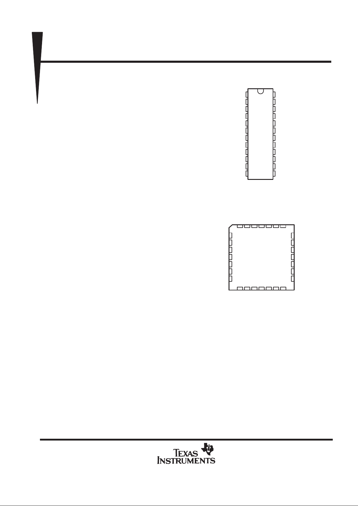
C SUFFIX . . . NT PACKAGE
M SUFFIX . . . JT PACKAGE
(TOP VIEW)
3212827
12 13
5
6
7
8
9
10
11
25
24
23
22
21
20
19
I/O/Q
I/O/Q
I/O/Q
NC
I/O/Q
I/O/Q
I/O/Q
I
I
I
NC
I
I
I
426
14 15 16 1718
I
I
GND
NC
I
I/O/Q
I/O/Q
I
I
CLK/INCI/O/Q
I/O/Q
C SUFFIX . . . FN PACKAGE
M SUFFIX . . . FK PACKAGE
(TOP VIEW)
NC
– No internal connection
Pin assignments in operating mode
V
CC

TIBPAL22V10C, TIBPAL22V10AC, TIBPAL22V10AM
HIGH-PERFORMANCE IMPACT PROGRAMMABLE ARRAY LOGIC CIRCUITS
SRPS024 – D2943, OCTOBER 1986 – REVISED MARCH 1992
POST OFFICE BOX 655303 • DALLAS, TEXAS 75265
2
description (continued)
Further advantages can be seen in the introduction of variable product term distribution. This technique
allocates from 8 to 16 logical product terms to each output for an average of 12 product terms per output. This
variable allocation of terms allows far more complex functions to be implemented than in previously available
devices.
Circuit design is enhanced by the addition of a synchronous set and an asynchronous reset product term. These
functions are common to all registers. When the synchronous set product term is a logic 1, the output registers
are loaded with a logic 1 on the next low-to-high clock transition. When the asynchronous reset product term
is a logic 1, the output registers are loaded with a logic 0. The output logic level after set or reset depends on
the polarity selected during programming. Output registers can be preloaded to any desired state during testing.
Preloading permits full logical verification during product testing.
With features such as programmable output logic macrocells and variable product term distribution, the
TIBPAL22V10 and TIBPAL22V10A offer quick design and development of custom LSI functions with
complexities of 500 to 800 equivalent gates. Since each of the ten output pins may be individually configured
as inputs on either a temporary or permanent basis, functions requiring up to 21 inputs and a single output or
down to 12 inputs and 10 outputs are possible.
A power-up clear function is supplied that forces all registered outputs to a predetermined state after power is
applied to the device. Registered outputs selected as active-low power up with their outputs high. Registered
outputs selected as active-high power up with their outputs low.
A single security fuse is provided on each device to discourage unauthorized copying of fuse patterns. Once
blown, the verification circuitry is disabled and all other fuses will appear to be open.
The TIBPAL22V10C and TIBPAL22V10AC are characterized for operation from 0°C to 75°C. The
TIBPAL22V10AM is characterized for operation over the full military temperature range of –55°C to125°C.
TIBPAL22V10C, TIBPAL22V10AC, TIBPAL22V10AM
HIGH-PERFORMANCE IMPACT PROGRAMMABLE ARRAY LOGIC CIRCUITS
SRPS024 – D2943, OCTOBER 1986 – REVISED MARCH 1992
POST OFFICE BOX 655303 • DALLAS, TEXAS 75265
3
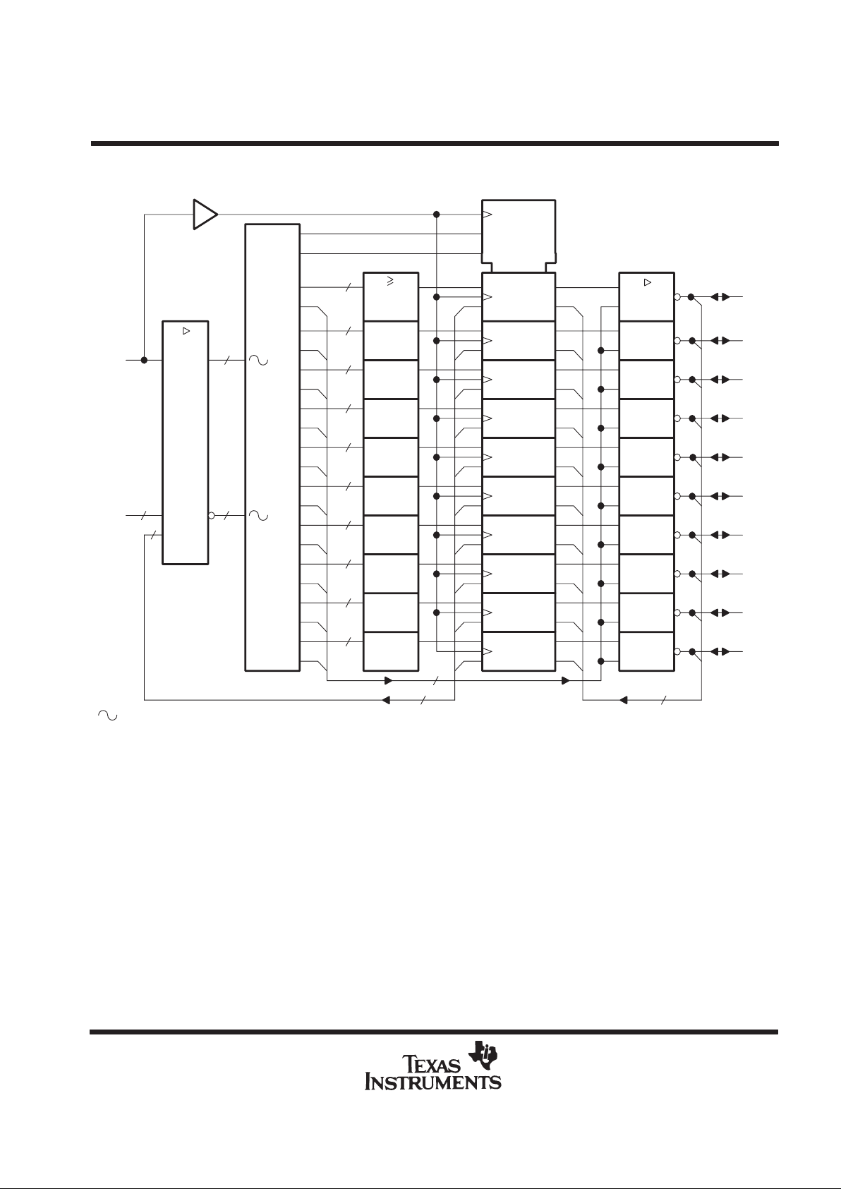
functional block diagram (positive logic)
I/O/Q
I/O/Q
I/O/Q
I/O/Q
I/O/Q
I/O/Q
10
12
14
EN
16
16
14
12
10
22
22
1
10
&
44 x 132
I/O/Q
I/O/Q
I/O/Q
I/O/Q
EN
EN
EN
EN
EN
EN
EN
EN
EN
10
10
8
8
10
11
CLK/I
I
Set
Reset
1S
R
C1
denotes fused inputs
Output
Logic
Macrocell
TIBPAL22V10C, TIBPAL22V10AC, TIBPAL22V10AM
HIGH-PERFORMANCE IMPACT PROGRAMMABLE ARRAY LOGIC CIRCUITS
SRPS024 – D2943, OCTOBER 1986 – REVISED MARCH 1992
POST OFFICE BOX 655303 • DALLAS, TEXAS 75265
4
0 4 8 1216202428
Increments
First
Fuse
Numbers
32 36 40
Macrocell
R = 5809
P = 5808
R = 5811
P = 5810
R = 5813
P = 5812
R = 5815
P = 5814
R = 5817
P = 5816
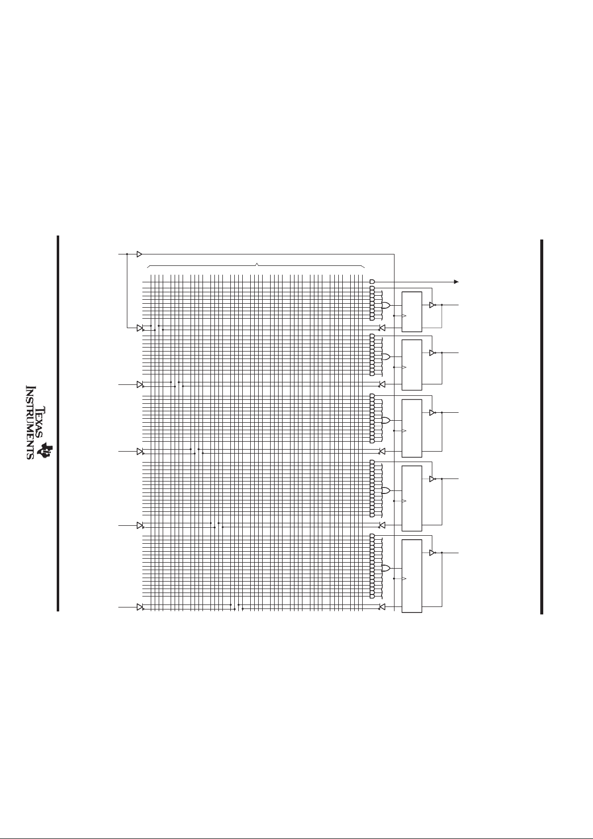
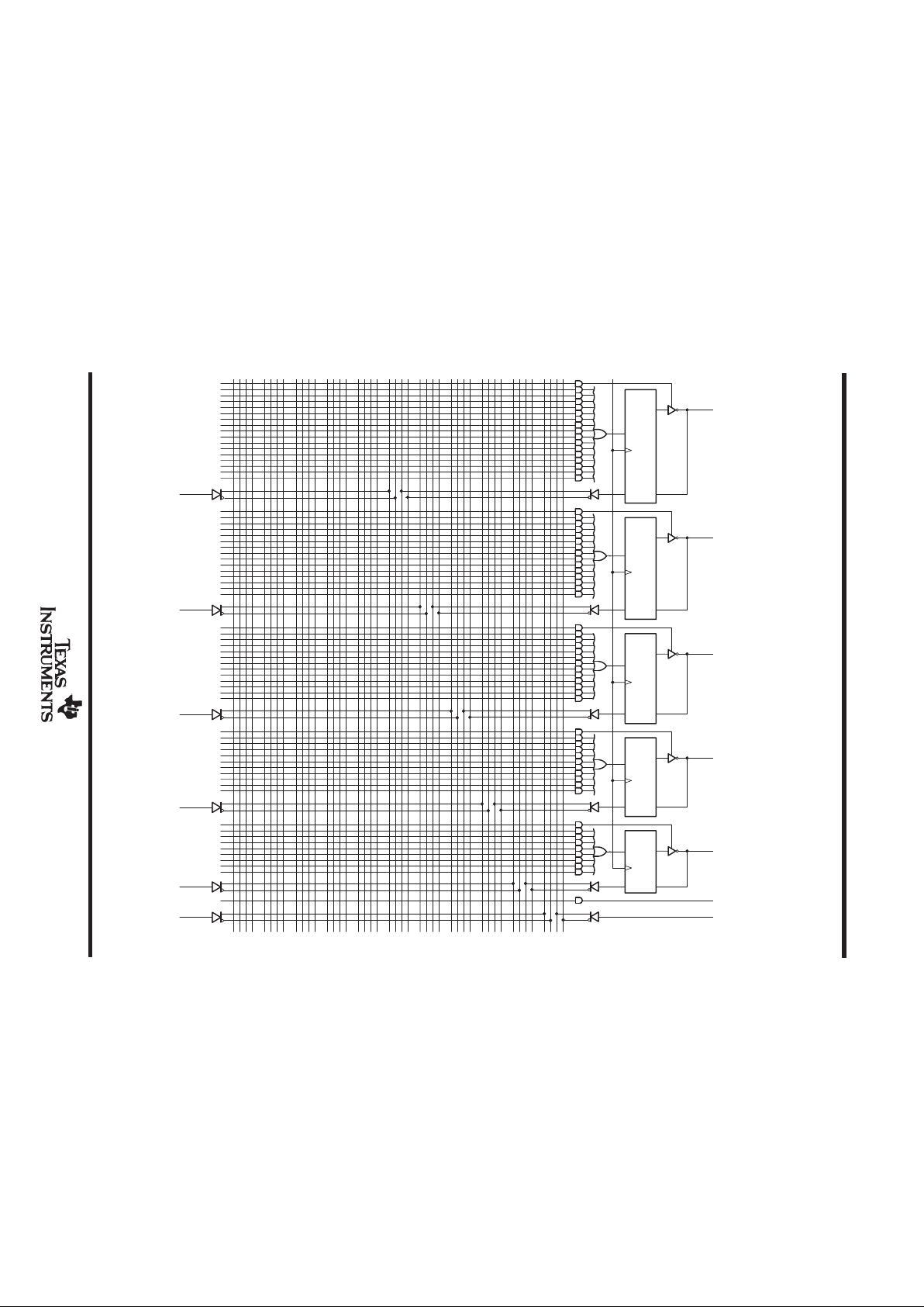
logic symbol (positive logic)
Asynchronous Reset
23
22
21
20
19
1
2
3
4
5
(to all registers)
396
0
440
880
924
1452
1496
2112
2156
2860
I/O/Q
I/O/Q
I/O/Q
I/O/Q
I/O/Q
I
I
I
I
CLK/I
Macrocell
Macrocell
Macrocell
Macrocell
TIBPAL22V10C, TIBPAL22V10AC, TIBPAL22V10AM
HIGH-PERFORMANCE IMPACT PROGRAMMABLE ARRAY LOGIC CIRCUITS
SRPS024 – D2943, OCTOBER 1986 – REVISED MARCH 1992
POST OFFICE BOX 655303 • DALLAS, TEXAS 75265
5
Fuse number = First fuse number + Increment
R = 5819
P = 5818
R = 5821
P = 5820
R = 5823
P = 5822
R = 5825
P = 5824
R = 5827
P = 5826
18
6
7
8
9
10
11
17
16
15
14
Synchronous Set
13
(to all registers)
Inside each MACROCELL the ”P” fuse is the polarity fuse and the ”R” fuse is the register fuse.
2904
3608
3652
4268
4312
4840
4884
5324
5368
5720
5764
I
I
I
I
I
I
I/O/Q
I/O/Q
I/O/Q
I/O/Q
I/O/Q
I
Macrocell
Macrocell
Macrocell
Macrocell
Macrocell
TIBPAL22V10C, TIBPAL22V10AC, TIBPAL22V10AM
HIGH-PERFORMANCE IMPACT PROGRAMMABLE ARRAY LOGIC CIRCUITS
SRPS024 – D2943, OCTOBER 1986 – REVISED MARCH 1992
POST OFFICE BOX 655303 • DALLAS, TEXAS 75265
6
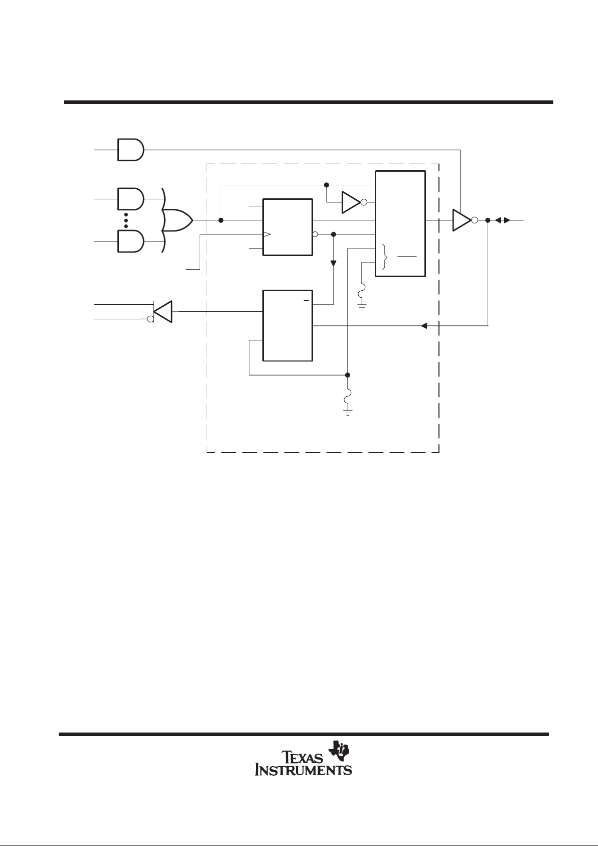
output logic macrocell diagram
C1
G
0
3
0
1
1
0
3
2
MUX
I = 0
1S
1D
R
MUX
G1
1
1
SS
AR
From Clock Buffer
S1
S0
AR = asynchronous reset
SS = synchronous set
Output Logic Macrocell
 Loading...