

Texas Instruments TIBPAL20L8-10CFN, TIBPAL20L8-10CNT, TIBPAL20R6-10CFN, TIBPAL20R6-10CNT, TIBPAL20R8-10CFN Datasheet
...
TIBPAL20L8-10C, TIBPAL20R4-10C, TIBPAL20R6-10C, TIBPAL20R8-10C
HIGH-PERFORMANCE IMPACT-X PAL
SRPS008A – D3336, OCTOBER 1989 – REVISED MARCH 1992
CIRCUITS
• High-Performance Operation:
f
(no feedback)
max
TIBPAL20R’ . . . 71.4 MHz
f
(internal feedback)
max
TIBPAL20R’...58.8 MHz
(external feedback)
f
max
TIBPAL20R’ . . . 55.5 MHz
Propagation Delay
TIBPAL20’ . . . 10 ns Max
• Functionally Equivalent, but Faster Than
Existing 24-Pin PLD Circuits
• Preload Capability on Output Registers
Simplifies Testing
• Power-Up Clear on Registered Devices (All
Register Outputs are Set Low, but Voltage
Levels at the Output Pins Go High)
• Package Options Include Plastic Chip
Carriers in Addition to Plastic and Ceramic
DIPs
• Security Fuse Prevents Duplication
• Dependable Texas Instruments Quality and
Reliability
DEVICE
PAL20L8 14 2 0 6
PAL20R4 12 0 4 (3-state buffers) 4
PAL20R6 12 0 6 (3-state buffers) 2
PAL20R8 12 0 8 (3-state buffers) 0
I
INPUTS
description
3-STATE
O OUTPUTS
REGISTERED
Q OUTPUTS
I/O
PORT
S
NC
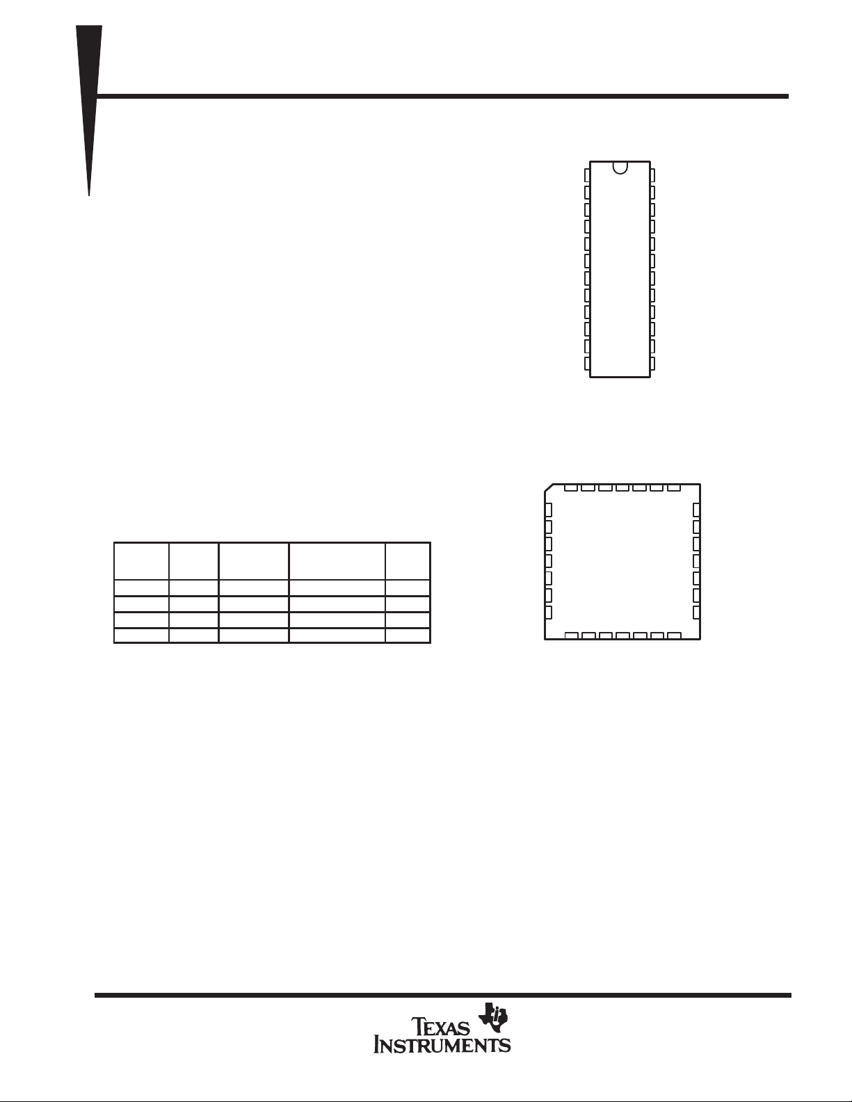
TIBPAL20L8’
JT OR NT PACKAGE
(TOP VIEW)
NC
NC
24
23
22
21
20
19
18
17
16
15
14
13
V
I
CC
V
I
O
I/O
I/O
I/O
I/O
I/O
I/O
O
I
I
I
I
CC
O
25
24
23
22
21
20
19
O
I
1
I
2
I
3
I
4
I
5
I
6
I
7
I
8
I
9
I
10
I
11
GND
I
I
I
I
I
I
12
TIBPAL20L8’
FN PACKAGE
(TOP VIEW)
I
I
I
3212827
426
5
6
7
8
9
10
11
12 13
14 15 16 17 18
I
I
GND
I/O
I/O
I/O
NC
I/O
I/O
I/O
These programmable array logic devices feature
high speed and functional equivalency when
NC
– No internal connection
Pin assignments in operating mode
compared with currently available devices. These
IMP ACT -X circuits combine the latest Advanced
Low-Power Schottky technology with proven titanium-tungsten fuses to provide reliable, high-performance
substitutes for conventional TTL logic. Their easy programmability allows for quick design of custom functions
and typically results in a more compact circuit board. In addition, chip carriers are available for futher reduction
in board space.
All of the register outputs are set to a low level during power up. Extra circuitry has been provided to allow loading
of each register asynchronously to either a high or low state. This feature simplifies testing because the registers
can be set to an initial state prior to executing the test sequence.
The TIBPAL20’ C series is characterized from 0°C to 75°C.
These devices are covered by U.S. Patent 4,410,987.
IMPACT-X is a trademark of Texas Instruments Incorporated.
PAL is a registered trademark of Advanced Micro Devices Inc.
PRODUCTION DATA information is current as of publication date.
Products conform to specifications per the terms of Texas Instruments
standard warranty. Production processing does not necessarily
include testing of all parameters.
POST OFFICE BOX 655303 • DALLAS, TEXAS 75265
Copyright 1992, Texas Instruments Incorporated
1
TIBPAL20R4-10C, TIBPAL20R6-10C, TIBPAL20R8-10C
HIGH-PERFORMANCE IMPACT-X PAL
SRPS008A – D3336, OCTOBER 1989 – REVISED MARCH 1992
CIRCUITS
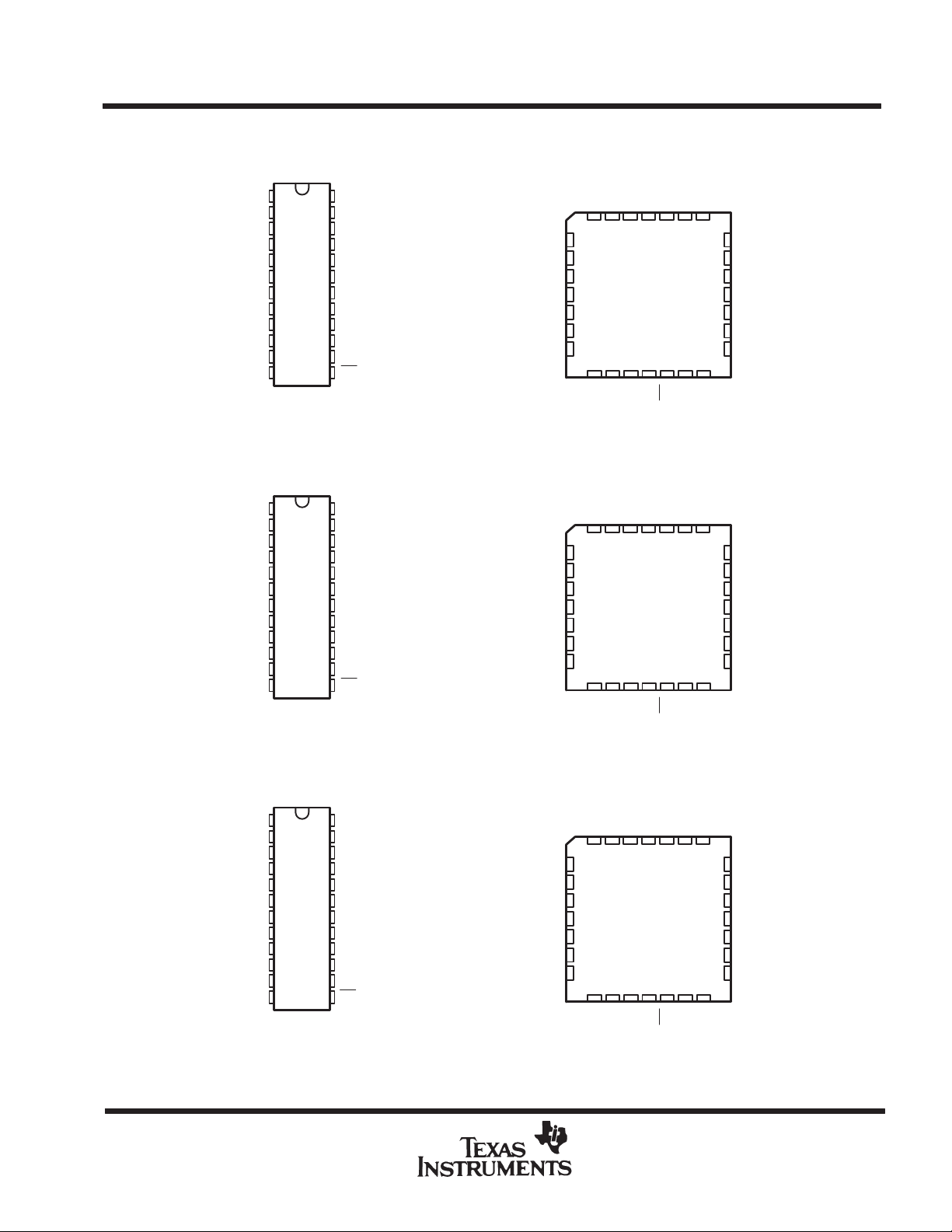
TIBPAL20R4’
JT OR NT PACKAGE
(TOP VIEW)
1
CLK
I
I
I
I
I
I
I
I
I
I
GND
TIBPAL20R6’
JT OR NT PACKAGE
CLK
I
I
I
I
I
I
I
I
I
I
GND
24
2
23
3
22
4
21
5
20
6
19
7
18
8
17
9
16
10
15
11
14
12
13
(TOP VIEW)
1
24
2
23
3
22
4
21
5
20
6
19
7
18
8
17
9
16
10
15
11
14
12
13
V
I
I/O
I/O
Q
Q
Q
Q
I/O
I/O
I
OE
V
I
I/O
Q
Q
Q
Q
Q
Q
I/O
I
OE
CC
CC
TIBPAL20R4’
FN PACKAGE
(TOP VIEW)
CC
I
I
4
3 2 1 282726
5 I/O
I
6
I
7
I
8
NC
9
I
10
I
11 19
I
12 13 14 15 16 17 18
I
I
TIBPAL20R6’
FN PACKAGE
(TOP VIEW)
I
I
4
3 2 1 282726
5Q
I
6
I
7
I
8
NC
9
I
10
I
11 19
I
12 13 14 15 16 17 18
I
I
V
CLKNCI
OE
NC
GND
CC
V
CLKNCI
OE
NC
GND
I/O
25
Q
24
Q
23
NC
22
Q
21
Q
20
I/O
I
I/O
I/O
25
Q
24
Q
23
NC
22
Q
21
Q
20
Q
I
I/O
TIBPAL20R8’
JT OR NT PACKAGE
(TOP VIEW)
1
CLK
2
I
3
I
4
I
5
I
6
I
7
I
8
I
9
I
10
I
11
I
12
GND
Pin assignments in operating mode
2
24
23
22
21
20
19
18
17
16
15
14
13
V
CC
I
Q
Q
Q
Q
Q
Q
Q
Q
I
OE
POST OFFICE BOX 655303 • DALLAS, TEXAS 75265
TIBPAL20R8’
FN PACKAGE
(TOP VIEW)
I
I
4
3 2 1 282726
5Q
I
6
I
7
I
8
NC
9
I
10
I
11
I
12 13 14 15 16 17 18
I
I
– No internal connection
NC
CC
CLKNCI
V
NC
OE
GND
Q
25
Q
24
Q
23
NC
22
Q
21
Q
20
19
Q
I
Q
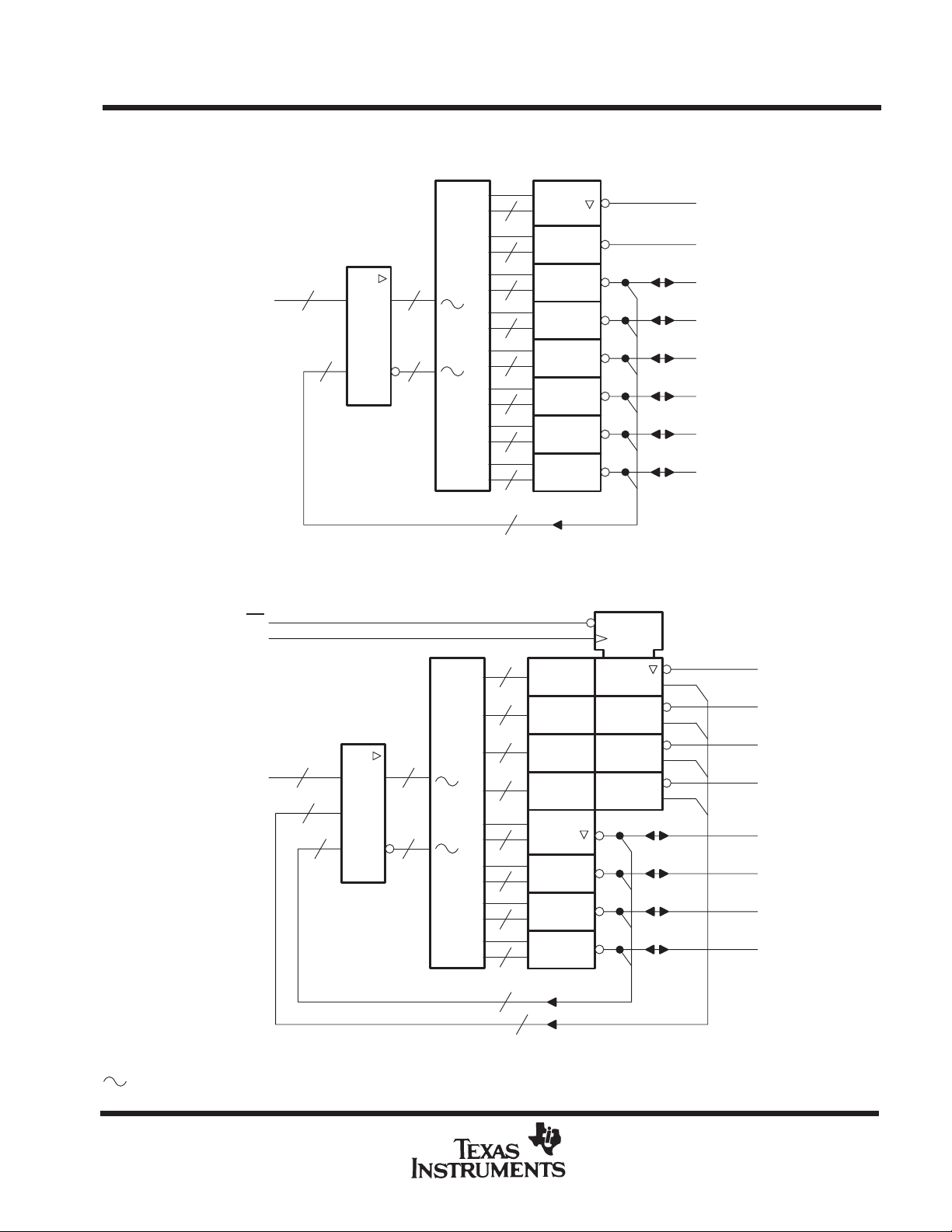
functional block diagrams (positive logic)
TIBPAL20L8-10C, TIBPAL20R4-10C
HIGH-PERFORMANCE IMPACT-X PAL
SRPS008A – D3336, OCTOBER 1989 – REVISED MARCH 1992
TIBPAL20L8’
CIRCUITS
OE
CLK
14 20
I
20 x
&
40 X 64
206
TIBPAL20R4’
7
7
7
7
7
7
7
7
6
EN
≥1
O
O
I/O
I/O
I/O
I/O
I/O
I/O
EN 2
C1
denotes fused inputs
12 20
I
4
20 x
1D
I = 0
2
Q
Q
Q
Q
I/O
I/O
I/O
I/O
&
40 X 64
204
8
8
8
8
7
7
7
7
4
≥1
≥1
EN
4
POST OFFICE BOX 655303 • DALLAS, TEXAS 75265
3
TIBPAL20R6-10C, TIBPAL20R8-10C
HIGH-PERFORMANCE IMPACT-X PAL
SRPS008A – D3336, OCTOBER 1989 – REVISED MARCH 1992
functional block diagrams (positive logic)
CIRCUITS
TIBPAL20R6’
OE
CLK
12 20
I
6
20 x
EN 2
C1
1D
I = 0
2
Q
Q
Q
Q
Q
Q
I/O
I/O
&
40 X 64
202
8
8
8
8
8
8
7
7
2
≥1
≥1
EN
6
CLK
denotes fused inputs
OE
12 20
I
20 x
TIBPAL20R8’
EN 2
C1
1D
I = 0
2
Q
Q
Q
Q
Q
Q
Q
Q
&
40 X 64
208
8
8
8
8
8
8
8
8
8
≥1
4
POST OFFICE BOX 655303 • DALLAS, TEXAS 75265
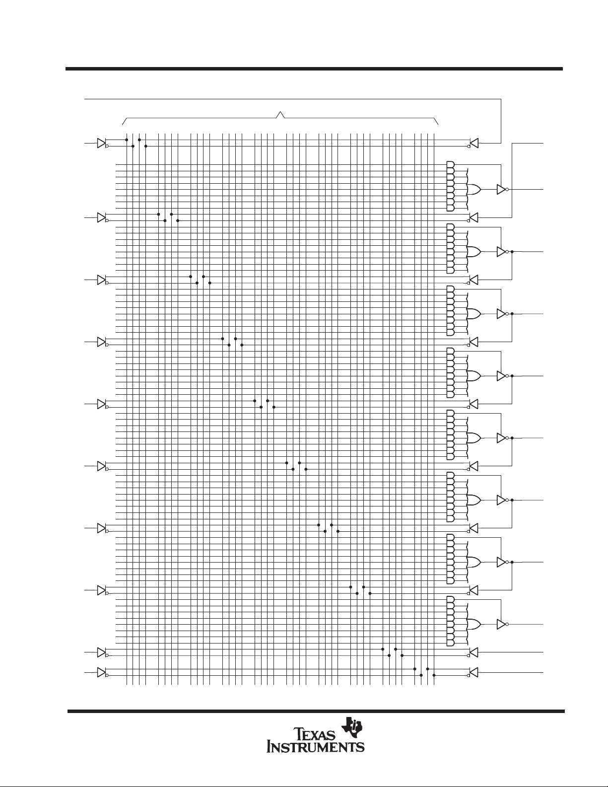
logic diagram (positive logic)
1
I
HIGH-PERFORMANCE IMPACT-X PAL
SRPS008A – D3336, OCTOBER 1989 – REVISED MARCH 1992
Increment
TIBPAL20L8-10C
CIRCUITS
2
I
First Fuse
Numbers
120
160
200
240
280
3
I
320
360
400
440
480
520
560
600
4
I
640
680
720
760
800
840
880
920
5
I
960
1000
1040
1080
1120
1160
1200
1240
6
I
1280
1320
1360
1400
1440
1480
1520
1560
7
I
1600
1640
1680
1720
1760
1800
1840
1880
8
I
1920
1960
2000
2040
2080
2120
2160
2200
9
I
2240
2280
2320
2360
2400
2440
2480
2520
10
I
11
I
4 8 12 16 20 24 28 32
0
40
80
36 390
23
I
22
O
21
I/O
20
I/O
19
I/O
18
I/O
17
I/O
16
I/O
15
O
14
I
13
I
Fuse number = First fuse number + Increment
Pin numbers shown are for JT and NT packages.
POST OFFICE BOX 655303 • DALLAS, TEXAS 75265
5
TIBPAL20R4-10C
HIGH-PERFORMANCE IMPACT-X PAL
SRPS008A – D3336, OCTOBER 1989 – REVISED MARCH 1992
logic diagram (positive logic)
1
CLK
Increment
CIRCUITS
2
I
First Fuse
Numbers
0
40
80
120
160
200
240
280
3
I
320
360
400
440
480
520
560
600
4
I
640
680
720
760
800
840
880
920
5
I
960
1000
1040
1080
1120
1160
1200
1240
6
I
1280
1320
1360
1400
1440
1480
1520
1560
7
I
1600
1640
1680
1720
1760
1800
1840
1880
8
I
1920
1960
2000
2040
2080
2120
2160
2200
9
I
2240
2280
2320
2360
2400
2440
2480
2520
10
I
11
I
Fuse number = First fuse number + Increment
Pin numbers shown are for JT and NT packages.
4 8 12 16 20 24 28 32
36 390
23
I
22
I/O
21
I/O
I = 0
1D
C1
I = 0
1D
C1
I = 0
1D
C1
I = 0
1D
C1
20
19
18
17
16
15
14
13
Q
Q
Q
Q
I/O
I/O
I
OE
6
POST OFFICE BOX 655303 • DALLAS, TEXAS 75265
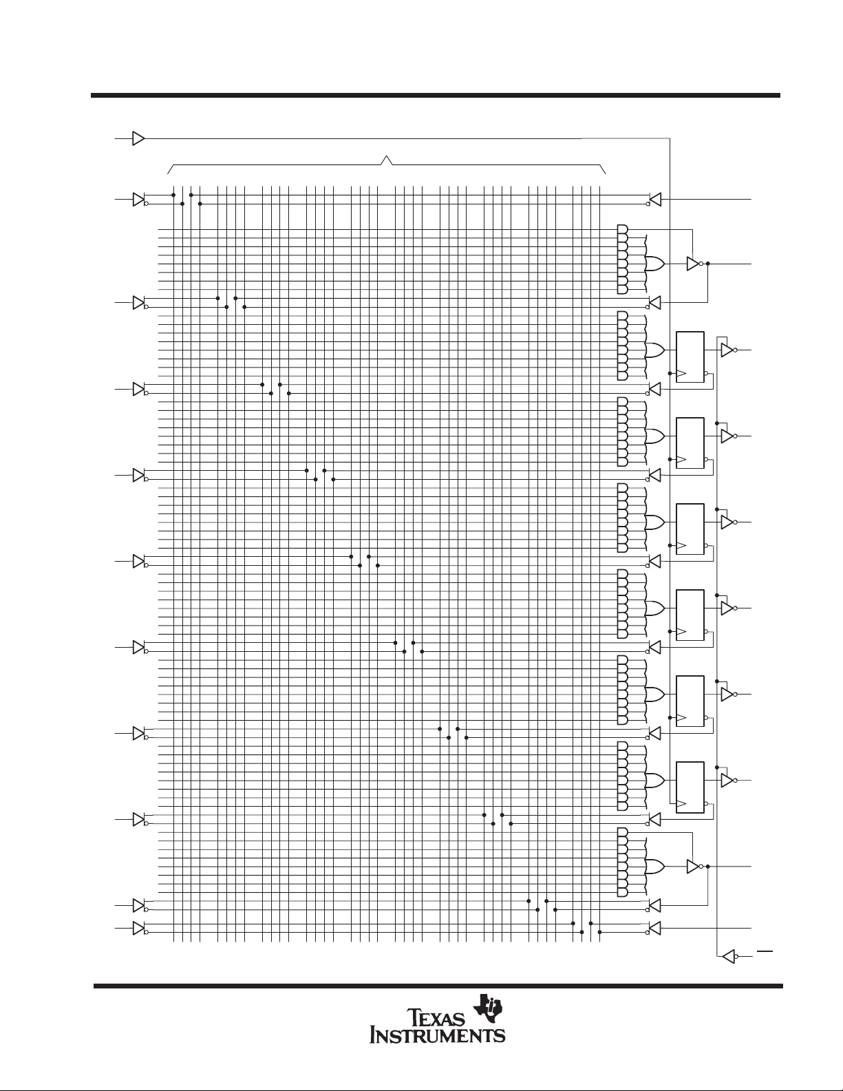
logic diagram (positive logic)
1
CLK
HIGH-PERFORMANCE IMPACT-X PAL
SRPS008A – D3336, OCTOBER 1989 – REVISED MARCH 1992
Increment
TIBPAL20R6-10C
CIRCUITS
2
I
First Fuse
Numbers
0
40
80
120
160
200
240
280
3
I
320
360
400
440
480
520
560
600
4
I
640
680
720
760
800
840
880
920
5
I
960
1000
1040
1080
1120
1160
1200
1240
6
I
1280
1320
1360
1400
1440
1480
1520
1560
7
I
1600
1640
1680
1720
1760
1800
1840
1880
8
I
1920
1960
2000
2040
2080
2120
2160
2200
9
I
2240
2280
2320
2360
2400
2440
2480
2520
10
I
11
I
Fuse number = First fuse number + Increment
Pin numbers shown are for JT and NT packages.
4 8 12 16 20 24 28 32
36 390
23
I
22
I/O
I = 0
1D
C1
I = 0
1D
C1
I = 0
1D
C1
I = 0
1D
C1
I = 0
1D
C1
I = 0
1D
C1
21
20
19
18
17
16
15
14
13
Q
Q
Q
Q
Q
Q
I/O
I
OE
POST OFFICE BOX 655303 • DALLAS, TEXAS 75265
7
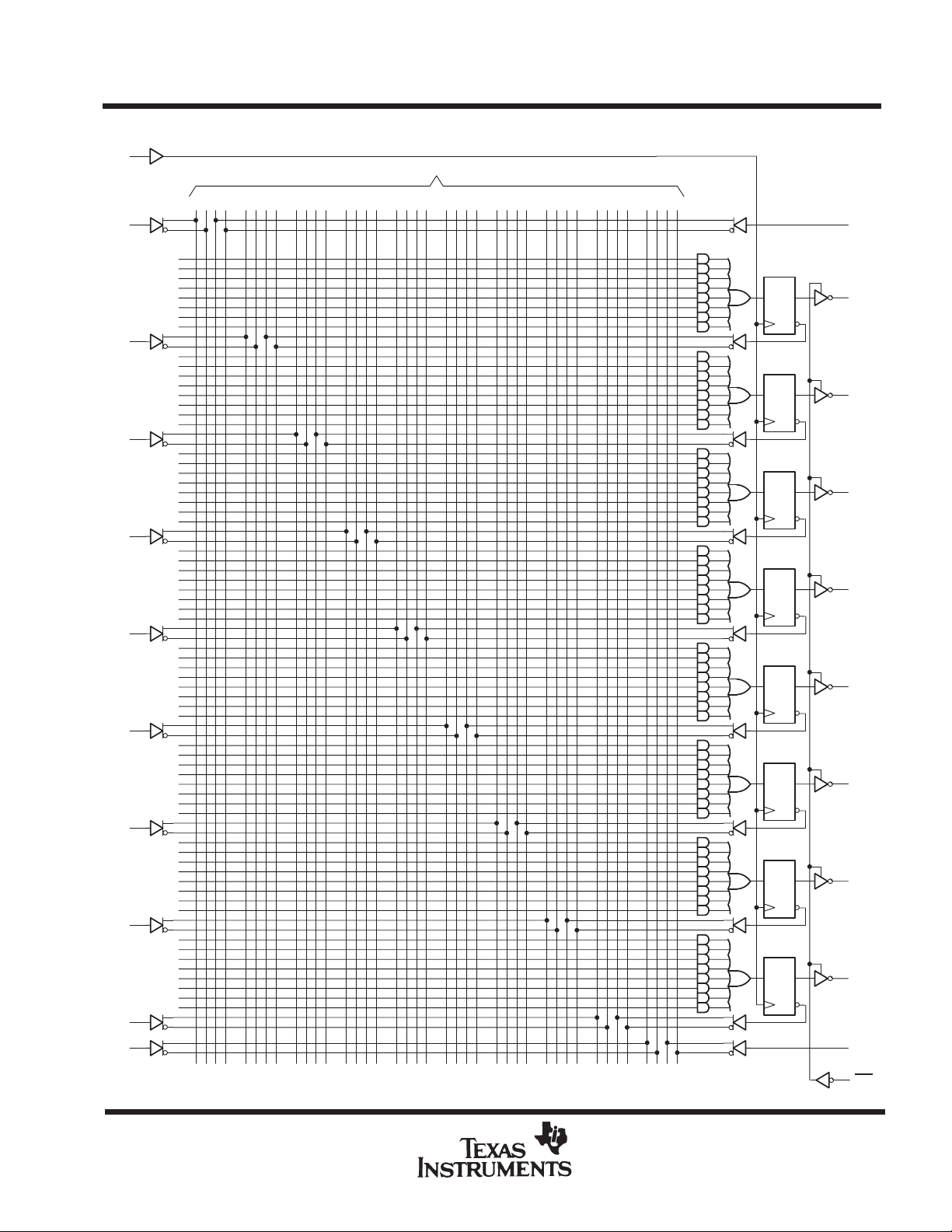
TIBPAL20R8-10C
HIGH-PERFORMANCE IMPACT-X PAL
SRPS008A – D3336, OCTOBER 1989 – REVISED MARCH 1992
logic diagram (positive logic)
1
CLK
Increment
CIRCUITS
2
I
First Fuse
Numbers
0
40
80
120
160
200
240
280
3
I
320
360
400
440
480
520
560
600
4
I
640
680
720
760
800
840
880
920
5
I
960
1000
1040
1080
1120
1160
1200
1240
6
I
1280
1320
1360
1400
1440
1480
1520
1560
7
I
1600
1640
1680
1720
1760
1800
1840
1880
8
I
1920
1960
2000
2040
2080
2120
2160
2200
9
I
2240
2280
2320
2360
2400
2440
2480
2520
10
I
11
I
Fuse number = First fuse number + Increment
Pin numbers shown are for JT and NT packages.
4 8 12 16 20 24 28 32
36 390
23
I
I = 0
1D
C1
I = 0
1D
C1
I = 0
1D
C1
I = 0
1D
C1
I = 0
1D
C1
I = 0
1D
C1
I = 0
1D
C1
I = 0
1D
C1
22
21
20
19
18
17
16
15
14
13
Q
Q
Q
Q
Q
Q
Q
Q
I
OE
8
POST OFFICE BOX 655303 • DALLAS, TEXAS 75265

TIBPAL20L8-10C, TIBPAL20R4-10C, TIBPAL20R6-10C, TIBPAL20R8-10C
HIGH-PERFORMANCE IMPACT-X PAL
SRPS008A – D3336, OCTOBER 1989 – REVISED MARCH 1992
absolute maximum ratings over operating free-air temperature range (unless otherwise noted)
Supply voltage, VCC (see Note 1) 7 V. . . . . . . . . . . . . . . . . . . . . . . . . . . . . . . . . . . . . . . . . . . . . . . . . . . . . . . . . . . .
Input voltage (see Note 1) 5.5 V. . . . . . . . . . . . . . . . . . . . . . . . . . . . . . . . . . . . . . . . . . . . . . . . . . . . . . . . . . . . . . . . . .
Voltage applied to disabled output (see Note 1) 5.5 V. . . . . . . . . . . . . . . . . . . . . . . . . . . . . . . . . . . . . . . . . . . . . . .
Operating free-air temperature range 0°C to 75°C. . . . . . . . . . . . . . . . . . . . . . . . . . . . . . . . . . . . . . . . . . . . . . . . . .
Storage temperature range –65°C to 150°C. . . . . . . . . . . . . . . . . . . . . . . . . . . . . . . . . . . . . . . . . . . . . . . . . . . . . . .
NOTE 1: These ratings apply except for programming pins during a programming cycle.
recommended operating conditions
MIN NOM MAX UNIT
V
CC
V
IH
V
IL
I
OH
I
OL
f
clock
†
w
†
t
su
†
t
h
T
A
†
f
clock
NOTE 2: These are absolute voltage levels with respect to the ground pin of the device and include all overshoots due to system and/or tester
Supply voltage 4.75 5 5.25 V
High-level input voltage 2 5.5 V
Low-level input voltage 0.8 V
High-level output current –3.2 mA
Low-level output current 24 mA
†
Clock frequency 0 71.4 MHz
Pulse duration, clock (see Note 2)t
Setup time, input or feedback before clock↑ 10 ns
Hold time, input or feedback after clock↑ 0 ns
Operating free-air temperature 0 25 75 °C
, tw, tsu, and th do not apply for TIBPAL20L8’.
noise. Testing these parameters should not be attempted without suitable equipment.
High 7
Low 7
CIRCUITS
ns
POST OFFICE BOX 655303 • DALLAS, TEXAS 75265
9
TIBPAL20L8-10C, TIBPAL20R4-10C, TIBPAL20R6-10C, TIBPAL20R8-10C
HIGH-PERFORMANCE IMPACT-X PAL
SRPS008A – D3336, OCTOBER 1989 – REVISED MARCH 1992
electrical characteristics over recommended operating free-air temperature range
PARAMETER TEST CONDITIONS MIN TYP†MAX UNIT
V
IK
V
OH
V
OL
I
OZH
I
OZL
I
I
I
IH
I
IL
I
OS
I
CC
C
i
C
o
C
clk
O, Q outputs 20
‡
I/O ports 100
O, Q outputs –20
‡
I/O ports –100
‡
‡
§
VCC = 4.75 V, II = –18 mA –0.8 –1.5 V
VCC = 4.75 V, IOH = –3.2 mA 2.4 V
VCC = 4.75 V, IOL = 24 mA 0.3 0.5 V
VCC = 5.25 V,
VCC = 5.25 V,
VCC = 5.25 V, VI = 5.5 V 0.2 mA
VCC = 5.25 V, VI = 2.7 V 25 µA
VCC = 5.25 V, VI = 0.4 V –0.25 mA
VCC = 5.25 V, VO = 0.5 V –30 –70 –130 mA
VCC = 5.25 V,
Outputs open,
f = 1 MHz, VI = 2 V 7 pF
f = 1 MHz, VO = 2 V 8 pF
f = 1 MHz, V
CIRCUITS
VO = 2.7 V
VO = 0.4 V
VI = 0,
= V
OE
IH
= 2 V 12 pF
CLK
µA
µA
210 mA
switching characteristics over recommended ranges of supply voltage and operating free-air
temperature (unless otherwise noted)
PARAMETER
¶
f
max
t
pd
t
pd
#
t
pd
t
en
t
dis
t
en
t
dis
||
t
sk(o)
†
All typical values are at VCC = 5 V, TA = 25°C.
‡
I/O leakage is the worst case of I
§
Not more than one output should be shorted at a time, and the duration of the short circuit should not exceed one second. VO is set at 0.5 V to
avoid test problems caused by test equipment ground degradation.
¶
See section for f
#
This parameter applies to TIBPAL20R4’ and TIBPAL20R6’ only (see Figure 4 for illustration) and is calculated from the measured f
feedback in the counter configuration.
||
This parameter is the measurement of the difference between the fastest and slowest tpd (CLK-to-Q) observed when multiple registered outputs
are switching in the same direction.
max
FROM
(INPUT)
without feedback 71.4
with internal feedback
(counter configuration)
with external feedback 55.5
I, I/O O, I/O R1 = 200 Ω, 3 8 10
CLK↑ Q R2 = 390 Ω, 2 5 8 ns
CLK↑ Feedback input See Figure 6 7 ns
OE↓ Q 2 6 10 ns
OE↑ Q 2 6 10 ns
I, I/O O, I/O 3 8 10 ns
I, I/O O, I/O 2 8 10 ns
Skew between registered outputs 0.5 ns
and IIL or I
OZL
specifications. f
max
OZH
does not apply for TIBPAL20L8’.
TO
(OUTPUT)
and IIH respectively.
TEST CONDITION MIN TYP†MAX UNIT
58.8 MHz
with internal
max
10
POST OFFICE BOX 655303 • DALLAS, TEXAS 75265

TIBPAL20L8-10C, TIBPAL20R4-10C, TIBPAL20R6-10C, TIBPAL20R8-10C
HIGH-PERFORMANCE IMPACT-X PAL
SRPS008A – D3336, OCTOBER 1989 – REVISED MARCH 1992
programming information
Texas Instruments programmable logic devices can be programmed using widely available software and
inexpensive device programmers.
Complete programming specifications, algorithms, and the latest information on hardware, software, and
firmware are available upon request. Information on programmers capable of programming T exas Instruments
programmable logic is also available, upon request, from the nearest TI field sales office, local authorized TI
distributor, or by calling Texas Instruments at (214) 997-5666.
preload procedure for registered outputs (see Figure 1 and Note 3)
The output registers can be preloaded to any desired state during device testing. This permits any state to be
tested without having to step through the entire state-machine sequence. Each register is preloaded individually
by following the steps given below.
Step 1. With V
at 5 volts and Pin 1 at VIL, raise Pin 13 to V
CC
Step 2. Apply either VIL or VIH to the output corresponding to the register to be preloaded.
Step 3. Pulse Pin 1, clocking in preload data.
Step 4. Remove output voltage, then lower Pin 13 to VIL. Preload can be verified by observing the
voltage level at the output pin.
Pin 13
t
Pin 1
t
t
d
su
t
w
.
IHH
d
CIRCUITS
V
IHH
V
IL
V
IH
V
IL
Registered I/O Input Output
NOTE 3: td = tsu = th = 100 ns to 1000 ns V
Figure 1. Preload Waveforms
= 10.25 V to 10.75 v
IHH
V
IH
V
IL
V
OH
V
OL
POST OFFICE BOX 655303 • DALLAS, TEXAS 75265
11
TIBPAL20L8-10C, TIBPAL20R4-10C, TIBPAL20R6-10C, TIBPAL20R8-10C
4 V
CIRCUITS
†
t
pd
(600 ns TYP, 1000 ns MAX)
1.5 V
1.5 V
t
w
‡
t
su
1.5 V
HIGH-PERFORMANCE IMPACT-X PAL
SRPS008A – D3336, OCTOBER 1989 – REVISED MARCH 1992
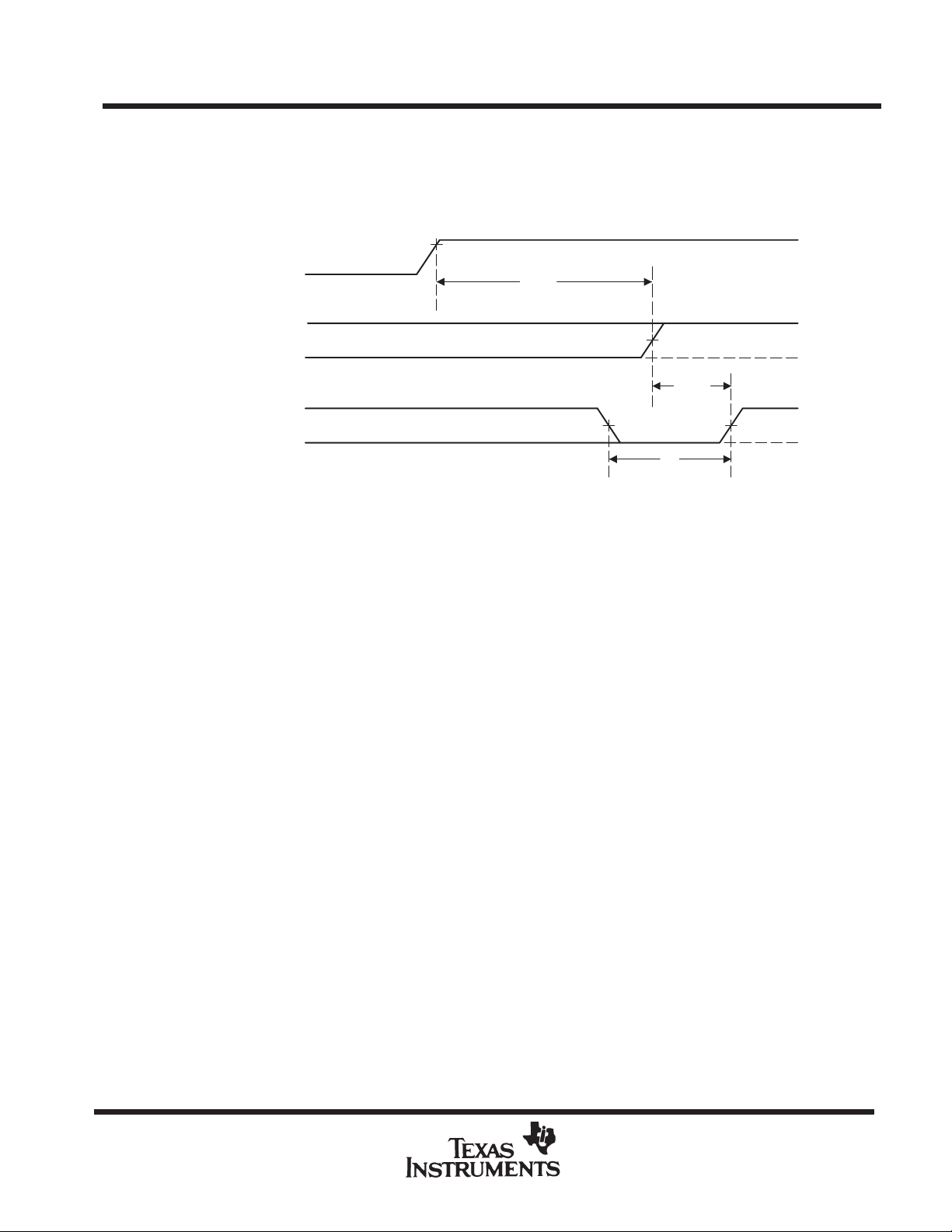
power-up reset (see Figure 2)
Following power up, all registers are reset to zero. This feature provides extra flexibility to the system designer
and is especially valuable in simplifying state-machine initialization. To ensure a valid power-up reset, it is
important that the rise of VCC be monotonic. Following power-up reset, a low-to-high clock transition must not
occur until all applicable input and feedback setup times are met.
V
CC
Active Low
Registered Output
CLK
5 V
V
V
V
V
OH
OL
IH
IL
†
This is the power-up reset time and applies to registered outputs only. The values shown are from characterization data.
‡
This is the setup time for input or feedback.
Figure 2. Power-Up Reset Waveforms
12
POST OFFICE BOX 655303 • DALLAS, TEXAS 75265

TIBPAL20L8-10C, TIBPAL20R4-10C, TIBPAL20R6-10C, TIBPAL20R8-10C
HIGH-PERFORMANCE IMPACT-X PAL
SRPS008A – D3336, OCTOBER 1989 – REVISED MARCH 1992
f
SPECIFICATIONS
max
without feedback, see Figure 3
f
max
In this mode, data is presented at the input to the flip-flop and clocked through to the Q output with no feedback.
Under this condition, the clock period is limited by the sum of the data setup time and the data hold time (t
However, the minimum f
f
Thus,
without feedback
max
is determined by the minimum clock period (tw high + tw low).
max
+
(twhigh
1
)
twlow)
CLK
or
1
(tsu)
th)
.
CIRCUITS
su
+ th).
f
with internal feedback, see Figure 4
max
LOGIC
ARRAY
tsu + t
tw high + tw low
Figure 3. f
h
or
Without Feedback
max
C1
1D
This configuration is most popular in counters and on-chip state-machine designs. The flip-flop inputs are
defined by the device inputs and flip-flop outputs. Under this condition, the period is limited by the internal delay
from the flip-flop outputs through the internal feedback and logic array to the inputs of the next flip-flop.
Thus,
f
with internal feedback
max
+
(tsu)
1
tpdCLK*to*FB)
.
Where tpd CLK-to-FB is the deduced value of the delay from CLK to the input of the logic array.
CLK
LOGIC
ARRAY
C1
1D
t
su
Figure 4. f
POST OFFICE BOX 655303 • DALLAS, TEXAS 75265
With Internal Feedback
max
tpd CLK-to-FB
13

TIBPAL20L8-10C, TIBPAL20R4-10C, TIBPAL20R6-10C, TIBPAL20R8-10C
HIGH-PERFORMANCE IMPACT-X PAL
SRPS008A – D3336, OCTOBER 1989 – REVISED MARCH 1992
with external feedback, see Figure 5
f
max
This configuration is a typical state-machine design with feedback signals sent off-chip. This external feedback
could go back to the device inputs or to a second device in a multi-chip state machine. The slowest path defining
the period is the sum of the clock-to-output time and the input setup time for the external signals
+ tpd CLK-to-Q).
(t
su
f
Thus,
with external feedback
max
CIRCUITS
f
SPECIFICATIONS
max
+
(tsu)
CLK
tpdCLK*to*Q)
1
.
LOGIC
ARRAY
t
su
Figure 5. f
C1
1D
tpd CLK-to-Q t
With External Feedback
max
NEXT DEVICE
su
14
POST OFFICE BOX 655303 • DALLAS, TEXAS 75265

TIBPAL20L8-10C, TIBPAL20R4-10C, TIBPAL20R6-10C, TIBPAL20R8-10C
HIGH-PERFORMANCE IMPACT-X PAL
SRPS008A – D3336, OCTOBER 1989 – REVISED MARCH 1992
PARAMETER MEASUREMENT INFORMATION
5 V
S1
R1
From Output
Under Test
Test
Point
CIRCUITS
Timing
Input
Data
Input
Input
In-Phase
Output
Out-of-Phase
Output
(see Note D)
1.5 V
t
su
1.5 V
VOLTAGE WAVEFORMS
SETUP AND HOLD TIMES
1.5 V 1.5 V
t
pd
1.5 V
t
pd
1.5 V 1.5 V
VOLTAGE WAVEFORMS
PROPAGATION DELAY TIMES
1.5 V
(see Note A)
3.5 V
0.3 V
t
h
3.5 V
0.3 V
3.5 V
0.3 V
t
pd
V
OH
1.5 V
V
OL
t
pd
V
OH
V
OL
C
L
LOAD CIRCUIT FOR
3-STATE OUTPUTS
High-Level
Output
Control
(low-level
enabling)
Waveform 1
S1 Closed
(see Note B)
Waveform 2
S1 Open
(see Note B)
R2
3.5 V
Pulse
Low-Level
Pulse
VOLTAGE WAVEFORMS
t
en
1.5 V 1.5 V
t
w
1.5 V 1.5 V
PULSE DURATIONS
1.5 V 1.5 V
t
dis
0.3 V
3.5 V
0.3 V
3.5 V
0.3 V
≈ 3.3 V
1.5 V
t
t
en
dis
1.5 V
VOL +0.5 V
V
V
VOH –0.5 V
≈ 0 V
ENABLE AND DISABLE TIMES, 3-STATE OUTPUTS
VOLTAGE WAVEFORMS
OL
OH
NOTES: A. CL includes probe and jig capacitance and is 50 pF for tpd and ten, 5 pF for t
B. Waveform 1 is for an output with internal conditions such that the output is low except when disabled by the output control. W aveform 2
is for an output with internal conditions such that the output is high except when disabled by the output control.
C. All input pulses have the following characteristics: PRR ≤ 1 MHz, tr = tf ≤ 2 ns, duty cycle = 50%.
D. When measuring propagation delay times of 3-state outputs, switch S1 is closed.
E. Equivalent loads may be used for testing.
Figure 6. Load Circuit and Voltage Waveforms
POST OFFICE BOX 655303 • DALLAS, TEXAS 75265
dis
.
15
TIBPAL20L8-10C, TIBPAL20R4-10C, TIBPAL20R6-10C, TIBPAL20R8-10C
HIGH-PERFORMANCE IMPACT-X PAL
SRPS008A – D3336, OCTOBER 1989 – REVISED MARCH 1992
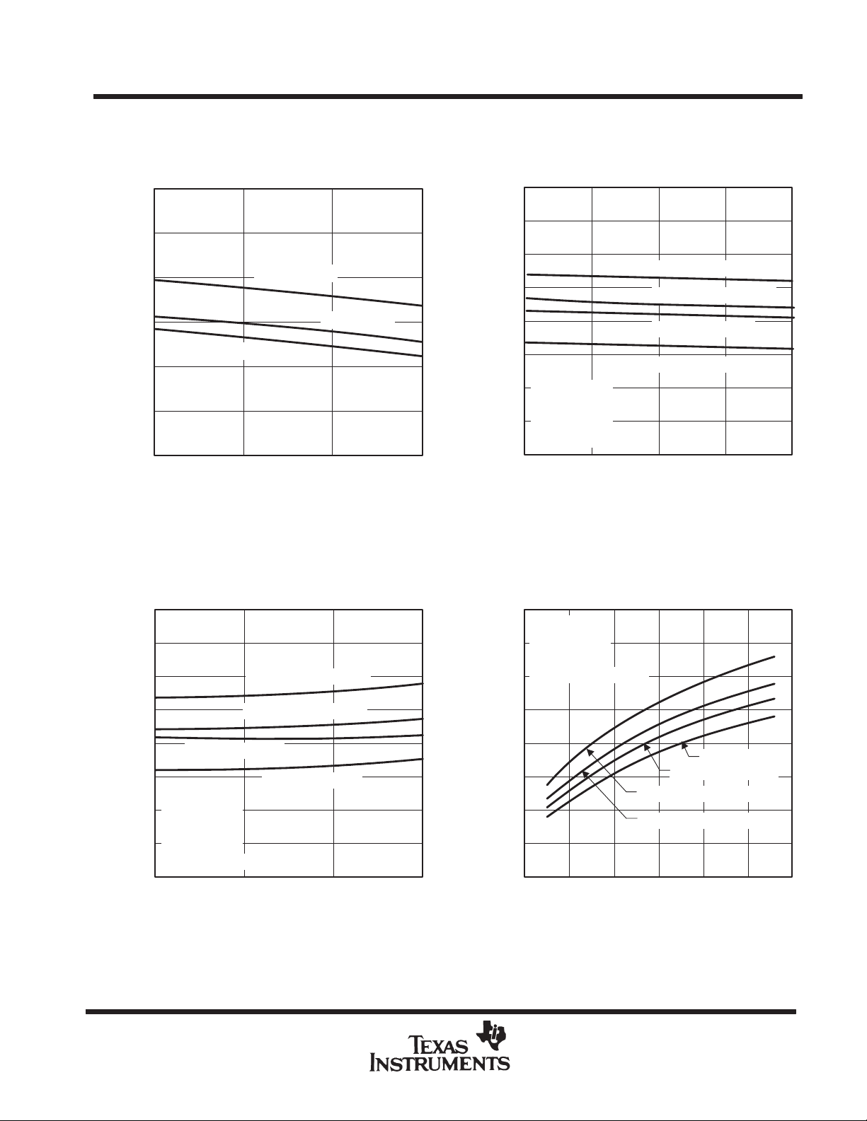
TYPICAL CHARACTERISTICS
SUPPLY CURRENT
vs
FREE-AIR TEMPERATURE
220
CIRCUITS
PROPAGATION DELAY TIME
SUPPLY VOLTAGE
8
vs
200
180
160
VCC = 4.75 V
140
– Supply Current – mA
CC
I
120
100
02550
TA – Free-Air T emperature – °C
VCC = 5.25 V
VCC = 5 V
Figure 7
PROPAGATION DELAY TIME
vs
FREE-AIR TEMPERATURE
8
7
t
6
(I, I/O to O, I/O)
PHL
75
7
6
5
4
3
TA = 25 °C
2
Propagation Delay Time – ns
CL = 50 pF
R1 = 200 Ω
1
R2 = 390 Ω
1 Output Switching
0
4.75 5
PROPAGATION DELAY TIME
16
VCC = 5 V
TA = 25 °C
14
R1 = 200 Ω
R2 = 390 Ω
1 Output Switching
12
t
(I, I/O to O, I/O)
PHL
t
(I, I/O to O, I/O)
PLH
t
(CLK to Q)
PHL
t
(CLK to Q)
PLH
VCC – Supply Voltage – V
Figure 8
vs
LOAD CAPACITANCE
5.25
16
t
5
Propagation Delay Time – ns
4
3
2
1
0
t
(CLK to Q)
PHL
VCC = 5 V
CL = 50 pF
R1 = 200 Ω
R2 = 390 Ω
1 Output Switching
02550
TA – Free-Air T emperature – °C
(I, I/O to O, I/O)
PLH
t
(CLK to Q)
PLH
Figure 9
10
8
6
4
Propagation Delay Time – ns
2
75
POST OFFICE BOX 655303 • DALLAS, TEXAS 75265
0
0 600
t
PHL
t
(I, I/O to O, I/O)
PHL
t
(I, I/O to O, I/O)
PLH
100 200 300 400
CL – Load Capacitance – pF
Figure 10
t
(CLK to Q)
PLH
(CLK to Q)
500

1000
900
VCC = 5 V
TA = 0 °C
TIBPAL20L8-10C, TIBPAL20R4-10C, TIBPAL20R6-10C, TIBPAL20R8-10C
TYPICAL CHARACTERISTICS
POWER DISSIPATION
vs
FREQUENCY
8-BIT COUNTER MODE
HIGH-PERFORMANCE IMPACT-X PAL
SRPS008A – D3336, OCTOBER 1989 – REVISED MARCH 1992
PROPAGATION DELAY TIME
vs
NUMBER OF OUTPUTS SWITCHING
0.8
VCC = 5 V
TA = 25 °C
0.7
R1 = 200 Ω
R2 = 390 Ω
CL = 50 pF
0.6
8-Bit Counter
0.5
CIRCUITS
†
800
– Power Dissipation – mW
700
D
P
600
TA = 25 °C
TA = 80 °C
1 4 10 40 100
F – Frequency – MHz
Figure 11
NUMBER OF OUTPUTS SWITCHING
8
7
6
t
PLH
5
0.4
0.3
0.2
– Skew Between Outputs Switching – ns
0.1
sk(o)
t
PROPAGATION DELAY TIME
vs
t
(I, I/O to O, I/O)
PHL
(I, I/O to O, I/O)
0
23 4 56
Number of Outputs Switching
Figure 12
78
4
3
2
Propagation Delay Time – ns
1
0
†
Outputs switching in the same direction (t
t
PHL
t
(CLK to Q)
PLH
VCC = 5 V
TA = 25 °C
CL = 50 pF
R1 = 200 Ω
R2 = 390 Ω
012345
Number of Outputs Switching
Figure 13
PLH compared to
POST OFFICE BOX 655303 • DALLAS, TEXAS 75265
t
PLH/tPHL to
t
(CLK to Q)
678
PHL)
17


TI Worldwide
Sales Offices
ALABAMA: Huntsville: 4960 Corporate Drive,
Suite 150, Huntsville, AL 35805, (205) 837-7530.
ARIZONA: Phoenix: 8825 N. 23rd Avenue, Suite 100,
Phoenix, AZ 85021, (602) 995-1007.
CALIFORNIA: Irvine: 1920 Main Street, Suite 900,
Irvine, CA 92714, (714) 660-1200;
San Diego: 5625 Ruffin Road, Suite 100,
San Diego, CA 92123, (619) 278-9600;
Santa Clara: 5353 Betsy Ross Drive,
Santa Clara, CA 95054, (408) 980-9000;
Woodland Hills: 21550 Oxnard Street, Suite 700,
Woodland Hills, CA 91367, (818) 704-8100.
COLORADO: Aurora: 1400 S. Potomac Street, Suite 101,
Aurora, CO 80012, (303) 368-8000.
CONNECTICUT: W allingford: 9 Barnes Industrial Park
So., Wallingford, CT 06492, (203) 269-0074.
FLORIDA: Altamonte Springs: 370 S. North Lake
Boulevard, Suite 1008, Altamonte Springs, FL 32701,
(407) 260-2116;
Fort Lauderdale: 2950 N.W. 62nd Street,
Suite 100, Fort Lauderdale, FL 33309,
(305) 973-8502; Tampa: 4803 George Road, Suite 390,
Tampa, FL 33634-6234, (813) 885-7588.
GEORGIA: Norcross: 5515 Spalding Drive,
Norcross, GA 30092-2560, (404) 662-7967.
ILLINOIS: Arlington Heights: 515 West Algonquin,
Arlington Heights, IL 60005, (708) 640-6925.
INDIANA: Carmel: 550 Congressional Drive, Suite 100,
Carmel, IN 46032, (317) 573-6400;
Fort Wayne: 103 Airport North Office Park,
Fort Wayne, IN 46825, (219) 489-4697.
KANSAS: Overland Park: 7300 College Boulevard,
Lighton Plaza, Suite 150, Overland Park, KS 66210,
(913) 451-4511.
MARYLAND: Columbia: 8815 Centre Park Drive,
Suite 100, Columbia, MD 21045, (410) 964-2003.
MASSACHUSETTS: Waltham: Bay Colony Corporate
Center 950 Winter Street, Suite 2800, Waltham, MA 02154,
(617) 895-9100.
MICHIGAN: Farmington Hills: 33737 W. 12 Mile Road,
Farmington Hills, MI 48018, (313) 553-1581.
MINNESOTA: Eden Prairie: 11000 W. 78th Street,
Suite 100, Eden Prairie, MN 55344, (612) 828-9300.
MISSOURI: St. Louis: 12412 Powerscourt Drive,
Suite 125, St. Louis, MO 63131, (314) 821-8400.
NEW JERSEY: Iselin: Metropolitan Corporate Plaza, 485
Bldg E. U.S. 1 South, Iselin, NJ 08830, (908) 750-1050.
NEW MEXICO: Albuquerque: 2709 J. Pan American
Freeway, N.E., Albuquerque, NM 87101, (505) 345-2555.
NEW YORK: East Syracuse: 6365 Collamer Drive,
East Syracuse, NY 13057, (315) 463-9291;
Fishkill: 300 Westage Business Center, Suite 140,
Fishkill, NY 12524, (914) 897-2900;
Melville: 48 South Service Road, Suite 100, Melville, NY
11747, (516) 454-6601;
Pittsford: 2851 Clover Street, Pittsford, NY 14534,
(716) 385-6770.
NORTH CAROLINA: Charlotte: 8 Woodlawn Green,
Suite 100, Charlotte, NC 28217, (704) 527-0930;
Raleigh: 2809 Highwoods Boulevard, Suite 100,
Raleigh, NC 27625, (919) 876-2725.
OHIO: Beachwood: 23775 Commerce Park Road,
Beachwood, OH 44122-5875, (216) 765-7258;
Beavercreek: 4200 Colonel Glenn Highway, Suite 600,
Beavercreek, OH 45431, (513) 427-6200.
OREGON: Beaverton: 6700 S.W. 105th Street,
Suite 110, Beaverton, OR 97005, (503) 643-6758.
PENNSYLVANIA: Blue Bell: 670 Sentry Parkway,
Suite 200, Blue Bell, PA 19422, (215) 825-9500.
PUERTO RICO: Hato Rey: 615 Mercantile Plaza Building,
Suite 505, Hato Rey, PR 00919, (809) 753-8700.
TEXAS: Austin: 12501 Research Boulevard,
Austin, TX 78759, (512) 250-6769;
Dallas: 7839 Churchill Way, Dallas, TX 75251,
(214) 917-1264;
Houston: 9301 Southwest Freeway, Commerce Park, Suite
360, Houston, TX 77074, (713) 778-6592;
Midland: FM 1788 & I-20, Midland, TX 79711-0448,
(915) 561-7137.
UTAH: Salt Lake City: 2180 South 1300 East, Sute 335,
Salt Lake City, UT 54106, (801) 466-8972.
WISCONSIN: Waukesha: 20825 Swenson Drive,
Suite 900, Waukesha WI 53186, (414) 798-1001.
CANADA: Nepean: 301 Moodie Drive, Suite 102, Mallom
Center, Nepean, Ontario, Canada K2H 9C4,
(613) 726-1970;
Richmond Hill: 280 Centre Street East, Richmond Hill,
Ontario, Canada L4C 1B1, (416) 884-9181;
St. Laurent: 9460 Trans Canada Highway, St. Laurent,
Quebec, Canada H4S 1R7, (514) 335-8392.
AUSTRALIA (& NEW ZEALAND): T exas Instruments
Australia Ltd., 6-10 Talavera Road, North Ryde (Sydney),
New South Wales, Australia 2113, 2-878-9000; 14th Floor,
380 Street, Kilda Road, Melbourne, Victoria, Australia 3004,
3-696-1211; 171 Philip Highway, Elizabeth, South Australia
5112, 8 255-2066.
BELGIUM: Texas Instruments Belgium S.A./N.V.,
Avenue Jules Bordetlaan 11, 1140 Brussels, Belgium,
(02) 242 30 80.
BRAZIL: Texas Instruments Electronicos do Brasil Ltda.,
Av. Eng. Luiz Carlos Berrini 1461-11o andar, 04571,
Sao Paulo, SP, Brazil, 11-535–5133.
DENMARK: Texas Instruments A/S, Borupvang 2D,
2750 Ballerup, Denmark, (44) 68 74 00.
FINLAND: Texas Instruments OY, Ahertajantle 3,
P.O. Box 86, 02321 Espoo, Finland, (0) 802 6517.
FRANCE: Texas Instruments France, 8-10 Avenue
Morane-Saulnier, B.P. 67, 78141 Velizy Villacoublay Cedex,
France, (1) 30 70 1003.
GERMANY: Texas Instruments Deutschland GmbH.,
Haggertystrasse 1, 8050 Freising, (08161) 80-0;
Kurfurstendamm 195-196, 1000 Berlin 15, (030) 8 82 73 65;
Dusseldorfer Strasse 40, 6236 Eschborn 1, (06196) 80 70;
Kirchhorster Strasse 2, 3000 Hannover 51, (0511) 64 68-0;
Maybachstrasse II, 7302 Ostfildern 2 (Nellingen),
(0711) 3403257; Gildehofcenter, Hollestrasses 3, 4300
Essen 1, (0201) 24 25-0.
HOLLAND: Texas Instruments Holland B.V., Hogehilweg
19, Postbus 12995, 1100 AZ Amsterdam-Zuidoost, Holland,
(020) 5602911.
HONG KONG: T exas Instruments Hong Kong Ltd., 8th
Floor, World Shipping Center, 7 Canton Road, Kowloon,
Hong Kong, 737-0338.
HUNGARY: Texas Instruments Representation, Budaorsi
ut.42, 1112 Budapest, Hungary, (1) 1 66 66 17.
IRELAND: Texas Instruments Ireland Ltd., 7/8 Harcourt
Street, Dublin 2, Ireland, (01) 755233.
ITALY: Texas Instruments Italia S.p.A., Centro Direzionale
Colleoni, Palazzo Perseo-Via Paracelso 12, 20041 Agrate
Brianza (Mi), Italy, (039) 63221; Via Castello della Magliana,
38, 00148 Roma, Italy (06) 6572651; Via Amendola, 17,
40100 Bologna, Italy (051) 554004.
JAPAN: Texas Instruments Japan Ltd., Aoyama Fuji
Building 3-6-12 Kita-Aoyama Minato-ku, Tokyo, Japan 107,
03-498-2111; MS Shibaura Building 9F, 4-13-23 Shibaura,
Minato-ku, Tokyo, Japan 108, 03-769-8700; Nissho-iwai
Building 5F, 2-5-8 Imabashi, Chuou-ku, Osaka, Japan 541,
06-204-1881; Dai-ni Toyota Building Nishi-kan 7F, 4-10-27
Meieki, Nakamura-ku, Nagoya, Japan 450, 052-583-8691;
Kanazawa Oyama-cho Daiichi Seimei Building 6F, 3-10
Oyama-cho, Kanazawa, Ishikawa, Japan 920,
0762-23-5471; Matsumoto Showa Building 6F, 1-2-11
Fukashi, Matsumoto, Nagano, Japan 390, 0263-33-1060;
Daiichi Olympic Tachikawa Building 6F, 1-25-12,
Akebono-cho, Tachikawa, Tokyo, Japan 190,
0425-27-6760; Yokohama Business Park East Tower 10F,
134 Goudo-cho Hodogaya-ku, Yokohama-shi, Kanagawa,
Japan 240, 045-338-1220; Nihon Seimei Kyoto Yasaka
Building 5F, 843-2, Higashi Shiokohji-cho, Higashi-iru,
Nishinotoh-in, Shiokohji-dori, Shimogyo-ku, Kyoto, Japan
600, 075-341-7713; Sumitomo Seimei Kumagaya Building
8F, 2-44 Yayoi, Kumagaya, Saitama, Japan 360,
0485-22-2440; 2597-1, Aza Harudai, Oaza Yasaka, Kitsuki,
Oita, Japan 873, 09786-3-3211.
KOREA: Texas Instruments Korea Ltd., 28th Floor, Trade
Tower, 159, Samsung-Dong, Kangnam-ku Seoul, Korea, 2
551-2800.
MALAYSIA: Texas Instruments Malaysia, Sdn. Bhd., Asia
Pacific, Lot 36.1 #Box 93, Menara Maybank, 100 Jalan Tun
Perak, 50050 Kuala Llumpur, Malaysia, 2306001.
MEXICO: Texas Instruments de Mexico S.A., de C.V.,
Alfonso Reyes 115, Col. Hipodromo Condesa, Mexico, D.F.,
Mexico 06170, 5-515-6081.
NORWAY: Texas Instruments Norge A/S, P.B. 106, Refstad
(Sinsenveien 53), 0513 Oslo 5, Norway, (02) 155 090.
PEOPLE’S REPUBLIC OF CHINA: Texas Instruments
China Inc., Beijing Representative Office, 7-05 CITIC
Building, 19 Jianguomenwai Dajie, Beijing, China,
500-2255, Ext. 3750.
PHILIPPINES: Texas Instruments Asia Ltd.,
Philippines Branch, 14th Floor, Ba-Lepanto Building,
Paseo de Roxas, Makati, Metro Manila, Philippines,
2-8176031.
PORTUGAL: Texas Instruments Equipamento Electronico
(Portugal) Ltda., Ing. Frederico Ulricho, 2650 Moreira Da
Maia, 4470 Maia, Portugal (2) 948 1003.
SINGAPORE (& INDIA, INDONESIA, MALAYSIA,
THAILAND): Texas Instruments Singapore (PTE) Ltd.,
Asia Pacific, 101 Thomson Road, #23-01,
United Square, Singapore 1130, 3508100.
SPAIN: Texas Instruments Espana S.A., c/Gobelas 43,
Urbanizasion, La Florida, 28023, Madrid, Spain, (1) 372
8051; c/Diputacion, 279-3-5, 08007 Barcelona, Spain, (3)
317 91 80.
SWEDEN: Texas Instruments International Trade
Corporation (Sverigefilialen), Isafjordsgaton, Box 30, S-164
93 Kista, Sweden, (08) 752 58 00.
SWITZERLAND: Texas Instruments Switzerland AG,
Riedstrasse 6, C8953 Dietikon, Switzerland,
(01) 744 2811.
TAIWAN: Texas Instruments Taiwan Limited, Taipei
Branch, 10th Floor Bank Tower, 205 Tung Hwa N. Road,
Taipei, Taiwan, 10592 Republic of China, 2-7139311.
TURKEY: Texas Instruments, DSEG MidEast Regional
Marketing Office, Karum Center, Suite 442, Iran Caddesi
21, 06680 Kavaklldere, Ankara, Turkey, 4-468-0155.
UNITED KINGDOM: T exas Instruments Ltd., Manton Lane,
Bedford, England, MK41 7PA, (0234) 270 111.
TI Authorized
North American
Distributors
Alliance Electronics, Inc. (military product only)
Almac/Arrow
Anthem Electronics
Arrow/Schweber
Future Electronics (Canada)
GRS Electronics Co., Inc. *
Hall-Mark Electronics
Marshall Industries
Newark Electronics *
Wyle Laboratories
Zeus Components
Rochester Electronics, Inc. (obsolete product only)
*Not authorized for TI military products
1992 T exas Instruments Incorporated
B0892

TI North
American Sales
Offices
ALABAMA: Huntsville: (205) 837-7530
ARIZONA: Phoenix: (602) 995-1007
CALIFORNIA: Irvine: (714) 660-1200
San Diego: (619) 278-9600
Santa Clara: (408) 980-9000
Woodland Hills: (818) 704-8100
COLORADO: Aurora: (303) 368-8000
CONNECTICUT: W allingford: (203) 269-0074
FLORIDA: Altamonte Springs: (407) 260-2116
Fort Lauderdale: (305) 973-8502
Tampa: (813) 885-7588
GEORGIA: Norcross: (404) 662-7967
ILLINOIS: Arlington Heights: (708) 640-3000
INDIANA: Carmel: (317) 573-6400
Fort Wayne: (219) 489-4697
KANSAS: Overland Park: (913) 451-4511
MARYLAND: Columbia: (410) 964-2003
MASSACHUSETTS: Waltham: (617) 895-9100
MICHIGAN: Farmington Hills: (313) 553-1581
MINNESOTA: Eden Prairie: (612) 828-9300
MISSOURI: St. Louis: (314) 821-8400
NEW JERSEY: Iselin: (908) 750-1050
NEW MEXICO: Albuquerque: (505) 345-2555
NEW YORK: East Syracuse: (315) 463-9291
Fishkill: (914) 897-2900
Melville: (516) 454-6600
Pittsford: (716) 385-6770
NORTH CAROLINA: Charlotte: (704) 527-0930
Raleigh: (919) 876-2725
OHIO: Beachwood: (216) 765-7258
Beavercreek: (513) 427-6200
OREGON: Beaverton: (503) 643-6758
PENNSYLVANIA: Blue Bell: (215) 825-9500
PUERTO RICO: Hato Rey: (809) 753-8700
TEXAS: Austin: (512) 250-6769
Dallas: (214) 917-1264
Houston: (713) 778-6592
Midland: (915) 561-7137
UTAH: Salt Lake CIty: (801) 466-8972
WISCONSIN: Waukesha: (414) 798-1001
CANADA: Nepean: (613) 726-1970
Richmond Hill: (416) 884-9181
St. Laurent: (514) 335-8392
TI Regional
Technology
Centers
CALIFORNIA: Irvine: (714) 660-8140
Santa Clara: (408) 748-2222
GEORGIA: Norcross: (404) 662-7945
ILLINOIS: Arlington Heights: (708) 640-2909
INDIANA: Indianapolis: (317) 573-6400
MASSACHUSETTS: Waltham: (617) 895-9196
MEXICO: Mexico City: 491-70834
MINNESOTA: Minneapolis: (612) 828-9300
TEXAS: Dallas: (214) 917-3881
CANADA: Nepean: (613) 726-1970
TI Authorized
North American
Distributors
Alliance Electronics, Inc. (military product only)
Almac/Arrow
Anthem Electronics
Arrow/Schweber
Future Electronics (Canada)
GRS Electronics Co., Inc.
Hall-Mark Electronics
Marshall Industries
Newark Electronics
Rochester Electronics, Inc.
(obsolete product only (508) 462-9332)
Wyle Laboratories
Zeus Components
TI Distributors
ALABAMA: Arrow/Schweber (205) 837-6955; Hall-Mark
(205) 837-8700; Marshall (205) 881-9235.
ARIZONA: Anthem (602) 966-6600; Arrow/Schweber (602)
437-0750; Hall-Mark (602) 431-0030; Marshall (602)
496-0290; Wyle (602) 437-2088.
CALIFORNIA: Los Angeles/Orange County: Anthem
(818) 775-1333, (714) 768-4444; Arrow/Schweber (818)
380-9686, (714) 838-5422; Hall-Mark (818) 773-4500, (714)
727-6000; Marshall (818) 878-7000, (714) 458-5301; Wyle
(818) 880-9000, (714) 863-9953; Zeus (714) 921-9000,
(818) 889-3838;
Sacramento: Anthem (916) 624-9744; Hall-Mark (916)
624-9781; Marshall (916) 635-9700; Wyle (916) 638-5282;
San Diego: Anthem (619) 453-9005; Arrow/Schweber
(619) 565-4800; Hall-Mark (619) 268-1201; Marshall (619)
578-9600; Wyle (619) 565-9171; Zeus (619) 277-9681.
San Francisco Bay Area: Anthem (408) 453-1200;
Arrow/Schweber (408) 441-9700, (510) 490-9477;
Hall-Mark (408) 432-4000; Marshall (408) 942-4600;
Wyle (408) 727-2500; Zeus (408) 629-4789.
COLORADO: Anthem (303) 790-4500; Arrow/Schweber
(303) 799-0258; Hall-Mark (303) 790-1662; Marshall (303)
451-8383; Wyle (303) 457-9953.
CONNECTICUT: Anthem (203) 575-1575; Arrow/Schweber
(203) 265-7741; Hall-Mark (203) 271-2844; Marshall (203)
265-3822.
FLORIDA:Fort Lauderdale:Arrow/Schweber (305)
429-8200; Halll-Mark (305) 971-9280; Marshall (305)
977-4880.
Orlando: Arrow/Schweber (407) 333-9300; Hall-Mark (407)
830-5855; Marshall (407) 767-8585; Zeus (407) 788-9100.
Tampa: Hall-Mark (813) 541-7440; Marshall (813)
573-1399.
GEORGIA: Arrow/Schweber (404) 497-1300; Hall-Mark
(404) 623-4400; Marshall (404) 923-5750.
ILLINOIS: Anthem (708) 884-0200; Arrow/Schweber (708)
250-0500; Hall-Mark (312) 860-3800; Marshall (708)
490-0155; Newark (312)784-5100.
INDIANA: Arrow/Schweber (317) 299-2071; Hall-Mark
(317) 872-8875; Marshall (317) 297-0483.
IOWA: Arrow/Schweber (319) 395-7230.
KANSAS: Arrow/Schweber (913) 541-9542; Hall-Mark
(913) 888-4747; Marshall (913) 492-3121.
MARYLAND: Anthem (301) 995-6640; Arrow/Schweber
(301) 596-7800; Hall-Mark (301) 988-9800; Marshall (301)
622-1118; Zeus (301) 997-1118.
MASSACHUSETTS: Anthem (508) 657-5170;
Arrow/Schweber (508) 658-0900; Hall-Mark (508)
667-0902; Marshall (508) 658-0810; Wyle (617) 272-7300;
Zeus (617) 246-8200.
MICHIGAN: Detroit: Arrow/Schweber (313) 462-2290;
Hall-Mark (313) 416-5800; Marshall (313) 525-5850;
Newark (313) 967-0600.
MINNESOTA: Anthem (612) 944-5454; Arrow/Schweber
(612) 941-5280; Hall-Mark (612) 881-2600; Marshall (612)
559-2211.
MISSOURI: Arrow/Schweber (314) 567-6888; Hall-Mark
(314) 291-5350; Marshall (314) 291-4650.
NEW JERSEY: Anthem (201) 227-7960; Arrow/Schweber
(201) 227-7880, (609) 596-8000; Hall-Mark (201) 515-3000,
(609) 235-1900; Marshall (201) 882-0320, (609) 234-9100.
NEW MEXICO: Alliance (505) 292-3360.
NEW YORK: Long Island: Anthem (516) 864-6600;
Arrow/Schweber (516) 231-1000; Hall-Mark (516)
737-0600; Marshall (516) 273-2424; Zeus (914) 937-7400.
Rochester: Arrow/Schweber (716) 427-0300; Hall-Mark
(716) 425-3300; Marshall (716) 235-7620.
Syracuse: Marshall (607) 785-2345.
NORTH CAROLINA: Arrow/Schweber (919) 876-3132;
Hall-Mark (919) 872-0712; Marshall (919) 878-9882.
OHIO: Cleveland: Arrow/Schweber (216) 248-3990;
Hall-Mark (216) 349-4632; Marshall (216) 248-1788.
Columbus: Hall-Mark (614) 888-3313.
Dayton: Arrow/Schweber (513) 435-5563; Marshall (513)
898-4480; Zeus (513) 293-6162.
OKLAHOMA: Arrow/Schweber (918) 252-7537; Hall-Mark
(918) 254-6110.
OREGON: Almac/Arrow (503) 629-8090; Anthem (503)
643-1114; Marshall (503) 644-5050; Wyle (503) 643-7900.
PENNSYLVANIA: Anthem (215) 443-5150;
Arrow/Schweber (215) 928-1800; GRS (215) 922-7037;
(609) 964-8560; Marshall (412) 788-0441.
TEXAS: Austin: Arrow/Schweber (512) 835-4180;
Hall-Mark (512) 258-8848; Marshall (512) 837-1991; Wyle
(512) 345-8853;
Dallas: Anthem (214) 238-7100; Arrow/Schweber (214)
380-6464; Hall-Mark (214) 553-4300; Marshall (214)
233-5200; Wyle (214) 235-9953; Zeus (214) 783-7010;
Houston: Arrow/Schweber (713) 530-4700; Hall-Mark
(713) 781-6100; Marshall (713) 467-1666; Wyle (713)
879-9953.
UTAH: Anthem (801) 973-8555; Arrow/Schweber (801)
973-6913; Marshall (801) 973-2288; Wyle (801) 974-9953.
WASHINGTON: Almac/Arrow (206) 643-9992, Anthem
(206) 483-1700; Marshall (206) 486-5747; Wyle (206)
881-1150.
WISCONSIN: Arrow/Schweber (414) 792-0150; Hall-Mark
(414) 797-7844; Marshall (414) 797-8400.
CANADA: Calgary: Future (403) 235-5325;
Edmonton: Future (403) 438-2858;
Montreal: Arrow/Schweber (514) 421-7411; Future (514)
694-7710; Marshall (514) 694-8142
Ottawa: Arrow/Schweber (613) 226-6903; Future (613)
820-8313.
Quebec: Future (418) 897-6666.
Toronto: Arrow/Schweber (416) 670-7769;
Future (416) 612-9200; Marshall (416) 458-8046.
Vancouver: Arrow/Schweber (604) 421-2333;
Future (604) 294-1166.
TI Die Processors
Chip Supply (407) 298-7100
Elmo Semiconductor (818) 768-7400
Minco T echnology Labs (512) 834-2022
Customer
Response Center
TOLL FREE: (800) 336-5236
OUTSIDE USA: (214) 995-6611
(8:00 a.m. – 5:00 p.m. CST)
1992 T exas Instruments Incorporated
D0892
SRPS008A

IMPORTANT NOTICE
T exas Instruments and its subsidiaries (TI) reserve the right to make changes to their products or to discontinue
any product or service without notice, and advise customers to obtain the latest version of relevant information
to verify, before placing orders, that information being relied on is current and complete. All products are sold
subject to the terms and conditions of sale supplied at the time of order acknowledgement, including those
pertaining to warranty, patent infringement, and limitation of liability.
TI warrants performance of its semiconductor products to the specifications applicable at the time of sale in
accordance with TI’s standard warranty. Testing and other quality control techniques are utilized to the extent
TI deems necessary to support this warranty . Specific testing of all parameters of each device is not necessarily
performed, except those mandated by government requirements.
CERTAIN APPLICA TIONS USING SEMICONDUCT OR PRODUCTS MAY INVOLVE POTENTIAL RISKS OF
DEATH, PERSONAL INJURY, OR SEVERE PROPERTY OR ENVIRONMENTAL DAMAGE (“CRITICAL
APPLICATIONS”). TI SEMICONDUCTOR PRODUCTS ARE NOT DESIGNED, AUTHORIZED, OR
WARRANTED TO BE SUITABLE FOR USE IN LIFE-SUPPORT DEVICES OR SYSTEMS OR OTHER
CRITICAL APPLICA TIONS. INCLUSION OF TI PRODUCTS IN SUCH APPLICATIONS IS UNDERST OOD TO
BE FULLY AT THE CUSTOMER’S RISK.
In order to minimize risks associated with the customer’s applications, adequate design and operating
safeguards must be provided by the customer to minimize inherent or procedural hazards.
TI assumes no liability for applications assistance or customer product design. TI does not warrant or represent
that any license, either express or implied, is granted under any patent right, copyright, mask work right, or other
intellectual property right of TI covering or relating to any combination, machine, or process in which such
semiconductor products or services might be or are used. TI’s publication of information regarding any third
party’s products or services does not constitute TI’s approval, warranty or endorsement thereof.
Copyright 1998, Texas Instruments Incorporated
 Loading...