

Texas Instruments TIBPAL20R8-5CNT, TIBPAL20R8-5CFN, TIBPAL20R8-7MWB, TIBPAL20R8-7MJTB, TIBPAL20R4-5CNT Datasheet
...
TIBPAL20L8-5C, TIBPAL20R4-5C, TIBPAL20R6-5C, TIBPAL20R8-5C
TIBPAL20L8-7M, TIBPAL20R4-7M, TIBPAL20R6-7M, TIBPAL20R8-7M
HIGH-PERFORMANCE IMPACT-X PAL
SRPS010F – D3353, OCTOBER 1989 – REVISED SEPTEMBER 1992
CIRCUITS
• High-Performance Operation:
f
(no feedback)
max
TIBPAL20R’ -5C Series . . . 125 MHz Min
TIBPAL20R’ -7M Series . . . 100 MHz Min
f
(internal feedback)
max
TIBPAL20R’ -5C Series . . . 125 MHz Min
TIBPAL20R’ -7M Series . . . 100 MHz Min
f
(external feedback)
max
TIBPAL20R’ -5C Series . . . 117 MHz Min
TIBPAL20R’ -7M Series . . . 74 MHz Min
Propagation Delay
TIBPAL20L8-5C Series . . . 5 ns Max
TIBPAL20L8-7M Series . . . 7 ns Max
TIBPAL20R’ -5C Series
(CLK-to-Q) . . . 4 ns Max
TIBPAL20R’ -7M Series
(CLK-to-Q) . . . 6.5 ns Max
• Functionally Equivalent, but Faster Than,
Existing 24-Pin PLDs
• Preload Capability on Output Registers
Simplifies Testing
• Power-Up Clear on Registered Devices (All
Register Outputs are Set Low, but Voltage
Levels at the Output Pins Go High)
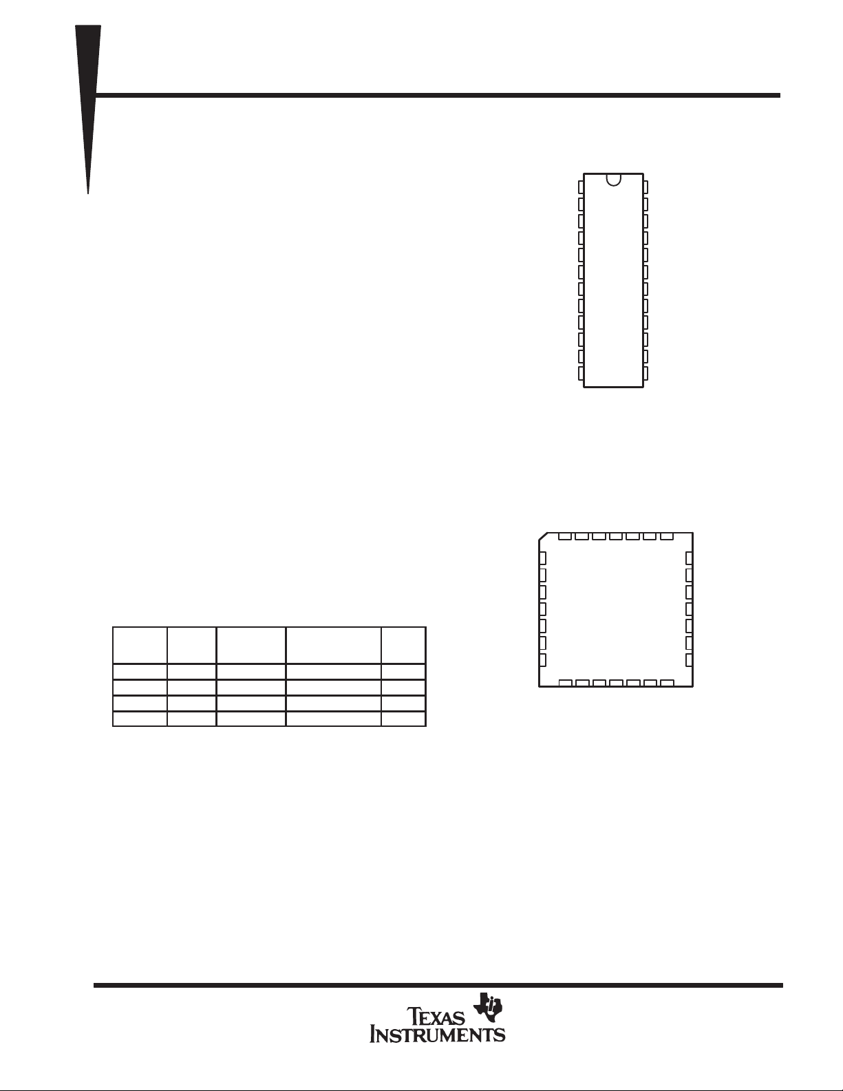
TIBPAL20L8’
C SUFFIX . . . JT OR NT PACKAGE
M SUFFIX . . . JT PACKAGE
(TOP VIEW)
NC
24
23
22
21
20
19
18
17
16
15
14
13
V
CC
V
I
O
I/O
I/O
I/O
I/O
I/O
I/O
O
I
I
I
CC
O
I
1
I
2
I
3
I
4
I
5
I
6
I
7
I
8
I
9
I
10
I
11
GND
C SUFFIX . . . FN PACKAGE
M SUFFIX . . . FK PACKAGE
12
TIBPAL20L8’
(TOP VIEW)
I
I
I
• Package Options Include Both Plastic and
Ceramic Chip Carriers in Addition to Plastic
and Ceramic DIPs
• Security Fuse Prevents Duplication
DEVICE
PAL20L8 14 2 0 6
PAL20R4 12 0 4 (3-state buffers) 4
PAL20R6 12 0 6 (3-state buffers) 2
PAL20R8 12 0 8 (3-state buffers) 0
I
INPUTS
description
3-STATE
O OUTPUTS
REGISTERED
Q OUTPUTS
I/O
PORT
S
I
I
I
NC
I
I
I
NC
– No internal connection
Pin assignments in operating mode
3212827
426
5
6
7
8
9
10
11
12 13
14 15 16 17 18
I
I
GND
NC
I
I
25
24
23
22
21
20
19
O
I/O
I/O
I/O
NC
I/O
I/O
I/O
These programmable array logic devices feature high speed and functional equivalency when compared with
currently available devices. These IMPACT-X circuits combine the latest Advanced Low-Power Schottky
technology with proven titanium-tungsten fuses to provide reliable, high-performance substitutes for
conventional TTL logic. Their easy programmability allows for quick design of custom functions and typically
results in a more compact circuit board.
The TIBPAL20’ C series is characterized from 0°C to 75°C. The TIBPAL20’ M series is characterized for
operation over the full military temperature range of –55°C to 125°C.
These devices are covered by U.S. Patent 4,410,987.
IMPACT-X is a trademark of Texas Instruments Incorporated.
PAL is a registered trademark of Advanced Micro Devices Inc.
This document contains information on products in more than one
phase of development. The status of each device is indicated on the
page(s) specifying its electrical characteristics.
POST OFFICE BOX 655303 • DALLAS, TEXAS 75265
Copyright 1992, Texas Instruments Incorporated
1
TIBPAL20R4-5C, TIBPAL20R6-5C, TIBPAL20R8-5C
TIBPAL20R4-7M, TIBPAL20R6-7M, TIBPAL20R8-7M
HIGH-PERFORMANCE IMPACT-X PAL
SRPS010F – D3353, OCTOBER 1989 – REVISED SEPTEMBER 1992
CIRCUITS
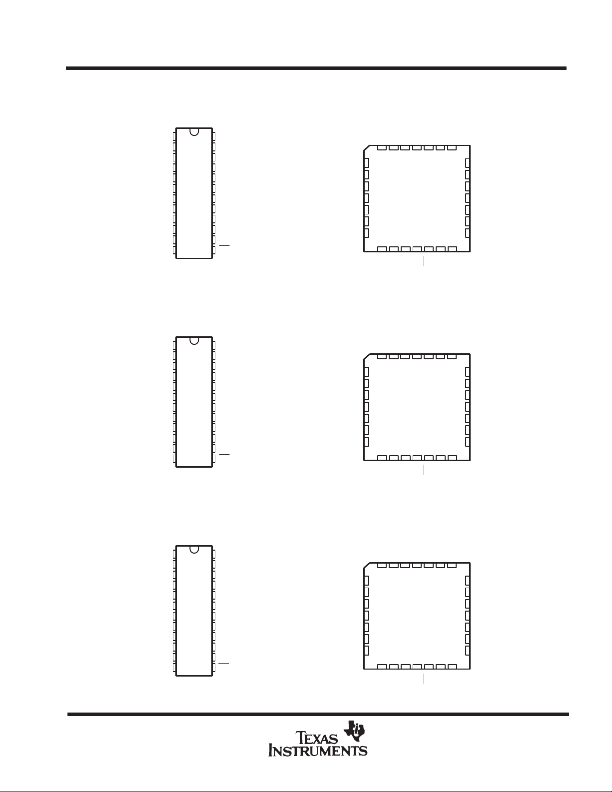
TIBPAL20R4’
C SUFFIX . . . JT OR NT PACKAGE
M SUFFIX . . . JT PACKAGE
(TOP VIEW)
24
23
22
21
20
19
18
17
16
15
14
13
24
23
22
21
20
19
18
17
16
15
14
13
V
I
I/O
I/O
Q
Q
Q
Q
I/O
I/O
I
OE
V
I
I/O
Q
Q
Q
Q
Q
Q
I/O
I
OE
CC
CC
1
CLK
2
I
3
I
4
I
5
I
6
I
7
I
8
I
9
I
10
I
11
I
12
GND
TIBPAL20R6’
C SUFFIX . . . JT OR NT PACKAGE
M SUFFIX . . . JT PACKAGE
(TOP VIEW)
1
CLK
2
I
3
I
4
I
5
I
6
I
7
I
8
I
9
I
10
I
11
I
12
GND
TIBPAL20R4’
C SUFFIX . . . FN PACKAGE
M SUFFIX . . . FK PACKAGE
(TOP VIEW)
CC
I
I
4
3 2 1 282726
5 I/O
I
6
I
7
I
8
NC
9
I
10
I
11
I
12 13 14 15 16 17 18
I
I
TIBPAL20R6’
C SUFFIX . . . FN PACKAGE
M SUFFIX . . . FK PACKAGE
(TOP VIEW)
I
I
4
3 2 1 282726
5Q
I
6
I
7
I
8
NC
9
I
10
I
11 19
I
12 13 14 15 16 17 18
I
I
V
CLKNCI
NC
OE
GND
CC
V
CLKNCI
OE
NC
GND
I/O
25
Q
24
Q
23
NC
22
Q
21
Q
20
19
I/O
I
I/O
I/O
25
Q
24
Q
23
NC
22
Q
21
Q
20
Q
I
I/O
TIBPAL20R8’
C SUFFIX . . . JT OR NT PACKAGE
M SUFFIX . . . JT PACKAGE
(TOP VIEW)
1
CLK
2
I
3
I
4
I
5
I
6
I
7
I
8
I
9
I
10
I
11
I
12
GND
Pin assignments in operating mode
2
24
23
22
21
20
19
18
17
16
15
14
13
V
CC
I
Q
Q
Q
Q
Q
Q
Q
Q
I
OE
POST OFFICE BOX 655303 • DALLAS, TEXAS 75265
TIBPAL20R8’
C SUFFIX . . . FN PACKAGE
M SUFFIX . . . FK PACKAGE
(TOP VIEW)
I
I
4
3 2 1 282726
5Q
I
6
I
7
I
8
NC
9
I
10
I
11 19
I
12 13 14 15 16 17 18
I
I
NC – No internal connection
CC
CLKNCI
V
OE
NC
GND
Q
25
Q
24
Q
23
NC
22
Q
21
Q
20
Q
I
Q
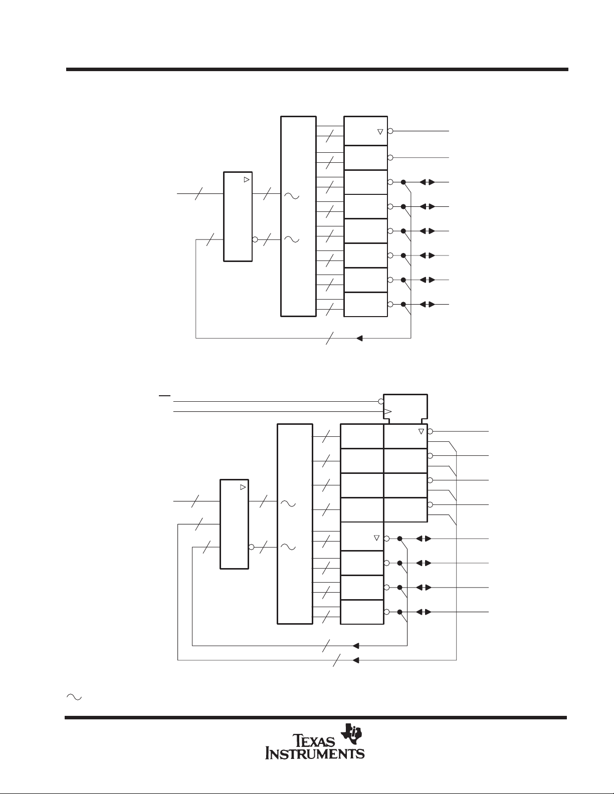
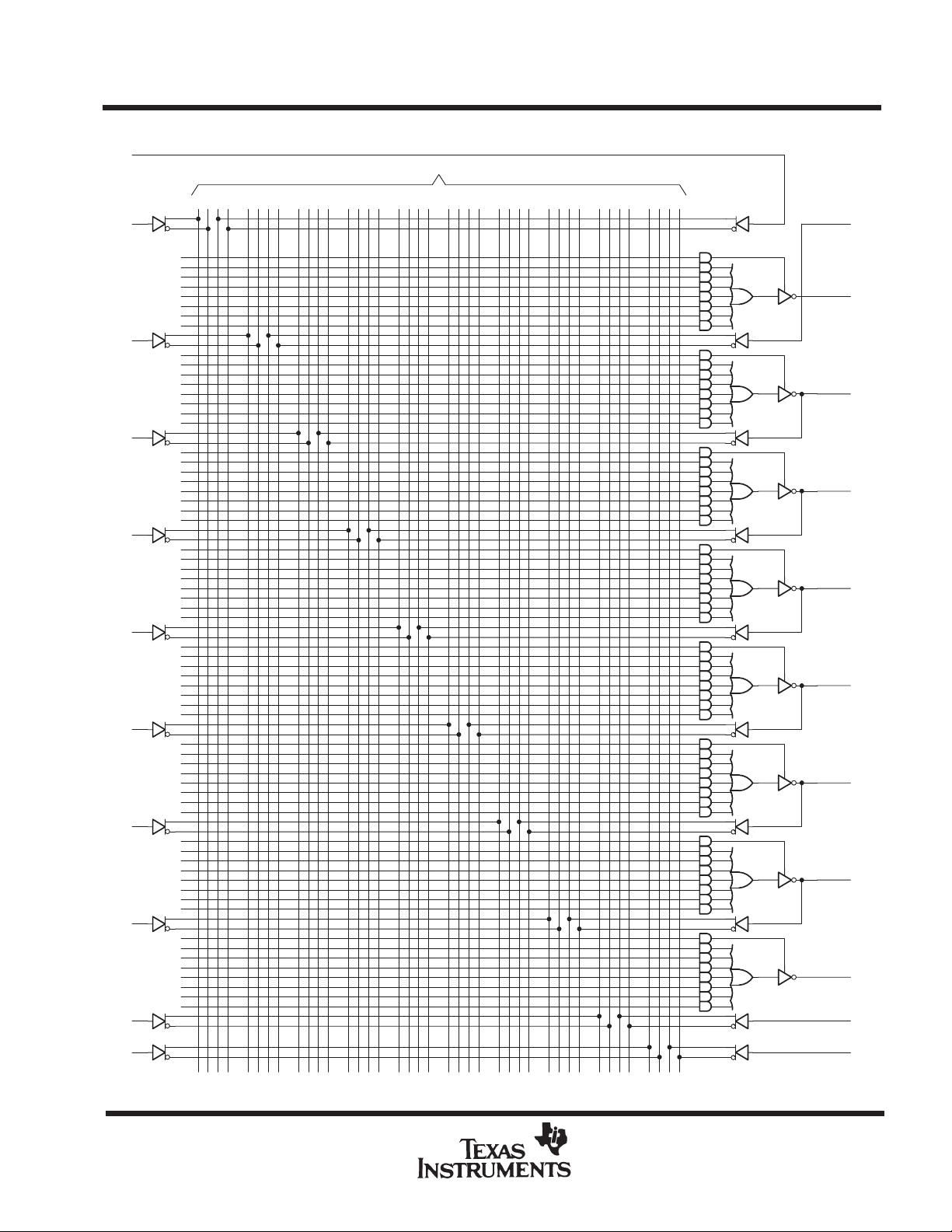
functional block diagrams (positive logic)
TIBPAL20L8-5C, TIBPAL20R4-5C
TIBPAL20L8-7M, TIBPAL20R4-7M
HIGH-PERFORMANCE IMPACT-X PAL
SRPS010F – D3353, OCTOBER 1989 – REVISED SEPTEMBER 1992
TIBPAL20L8’
CIRCUITS
OE
CLK
14 20
I
20 x
&
40 X 64
206
TIBPAL20R4’
7
7
7
7
7
7
7
7
6
EN
≥1
O
O
I/O
I/O
I/O
I/O
I/O
I/O
EN 2
C1
denotes fused inputs
12 20
I
4
20 x
1D
I = 0
2
Q
Q
Q
Q
I/O
I/O
I/O
I/O
&
40 X 64
204
8
8
8
8
7
7
7
7
4
≥1
≥1
EN
4
POST OFFICE BOX 655303 • DALLAS, TEXAS 75265
3
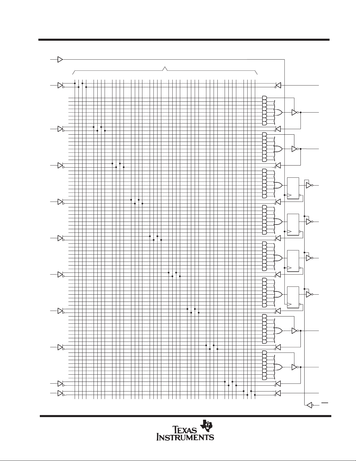
TIBPAL20R6-5C, TIBPAL20R8-5C
TIBPAL20R6-7M, TIBPAL20R8-7M
HIGH-PERFORMANCE IMPACT-X PAL
SRPS010F – D3353, OCTOBER 1989 – REVISED SEPTEMBER 1992
functional block diagrams (positive logic)
CIRCUITS
TIBPAL20R6’
OE
CLK
12 20
I
6
20 x
EN 2
C1
1D
I = 0
2
Q
Q
Q
Q
Q
Q
I/O
I/O
&
40 X 64
202
8
8
8
8
8
8
7
7
2
≥1
≥1
EN
6
CLK
denotes fused inputs
OE
12 20
I
20 x
TIBPAL20R8’
EN 2
C1
1D
I = 0
2
Q
Q
Q
Q
Q
Q
Q
Q
&
40 X 64
208
8
8
8
8
8
8
8
8
8
≥1
4
POST OFFICE BOX 655303 • DALLAS, TEXAS 75265
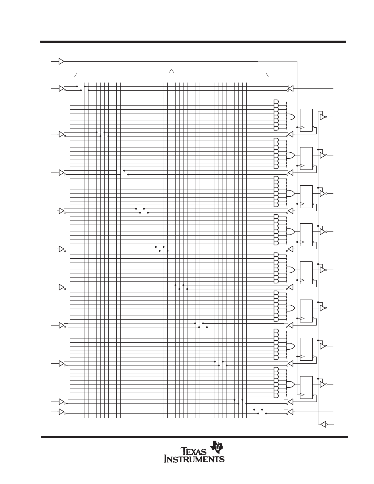
logic diagram (positive logic)
1
I
HIGH-PERFORMANCE IMPACT-X PAL
SRPS010F – D3353, OCTOBER 1989 – REVISED SEPTEMBER 1992
Increment
TIBPAL20L8-5C
TIBPAL20L8-7M
CIRCUITS
2
I
First Fuse
Numbers
120
160
200
240
280
3
I
320
360
400
440
480
520
560
600
4
I
640
680
720
760
800
840
880
920
5
I
960
1000
1040
1080
1120
1160
1200
1240
6
I
1280
1320
1360
1400
1440
1480
1520
1560
7
I
1600
1640
1680
1720
1760
1800
1840
1880
8
I
1920
1960
2000
2040
2080
2120
2160
2200
9
I
2240
2280
2320
2360
2400
2440
2480
2520
10
I
11
I
4 8 12 16 20 24 28 32
0
40
80
36 390
23
I
22
O
21
I/O
20
I/O
19
I/O
18
I/O
17
I/O
16
I/O
15
O
14
I
13
I
Fuse number = First fuse number + Increment
Pin numbers shown are for JT and NT packages.
POST OFFICE BOX 655303 • DALLAS, TEXAS 75265
5
TIBPAL20R4-5C
TIBPAL20R4-7M
HIGH-PERFORMANCE IMPACT-X PAL
SRPS010F – D3353, OCTOBER 1989 – REVISED SEPTEMBER 1992
logic diagram (positive logic)
1
CLK
Increment
CIRCUITS
2
I
First Fuse
Numbers
0
40
80
120
160
200
240
280
3
I
320
360
400
440
480
520
560
600
4
I
640
680
720
760
800
840
880
920
5
I
960
1000
1040
1080
1120
1160
1200
1240
6
I
1280
1320
1360
1400
1440
1480
1520
1560
7
I
1600
1640
1680
1720
1760
1800
1840
1880
8
I
1920
1960
2000
2040
2080
2120
2160
2200
9
I
2240
2280
2320
2360
2400
2440
2480
2520
10
I
11
I
Fuse number = First fuse number + Increment
Pin numbers shown are for JT and NT packages.
4 8 12 16 20 24 28 32
36 390
23
I
22
I/O
21
I/O
I = 0
1D
C1
I = 0
1D
C1
I = 0
1D
C1
I = 0
1D
C1
20
19
18
17
16
15
14
13
Q
Q
Q
Q
I/O
I/O
I
OE
6
POST OFFICE BOX 655303 • DALLAS, TEXAS 75265

logic diagram (positive logic)
1
CLK
HIGH-PERFORMANCE IMPACT-X PAL
SRPS010F – D3353, OCTOBER 1989 – REVISED SEPTEMBER 1992
Increment
TIBPAL20R6-5C
TIBPAL20R6-7M
CIRCUITS
2
I
First Fuse
Numbers
0
40
80
120
160
200
240
280
3
I
320
360
400
440
480
520
560
600
4
I
640
680
720
760
800
840
880
920
5
I
960
1000
1040
1080
1120
1160
1200
1240
6
I
1280
1320
1360
1400
1440
1480
1520
1560
7
I
1600
1640
1680
1720
1760
1800
1840
1880
8
I
1920
1960
2000
2040
2080
2120
2160
2200
9
I
2240
2280
2320
2360
2400
2440
2480
2520
10
I
11
I
Fuse number = First fuse number + Increment
Pin numbers shown are for JT and NT packages.
4 8 12 16 20 24 28 32
36 390
23
I
22
I/O
I = 0
1D
C1
I = 0
1D
C1
I = 0
1D
C1
I = 0
1D
C1
I = 0
1D
C1
I = 0
1D
C1
21
20
19
18
17
16
15
14
13
Q
Q
Q
Q
Q
Q
I/O
I
OE
POST OFFICE BOX 655303 • DALLAS, TEXAS 75265
7
TIBPAL20R8-5C
TIBPAL20R8-7M
HIGH-PERFORMANCE IMPACT-X PAL
SRPS010F – D3353, OCTOBER 1989 – REVISED SEPTEMBER 1992
logic diagram (positive logic)
1
CLK
Increment
CIRCUITS
2
I
First Fuse
Numbers
0
40
80
120
160
200
240
280
3
I
320
360
400
440
480
520
560
600
4
I
640
680
720
760
800
840
880
920
5
I
960
1000
1040
1080
1120
1160
1200
1240
6
I
1280
1320
1360
1400
1440
1480
1520
1560
7
I
1600
1640
1680
1720
1760
1800
1840
1880
8
I
1920
1960
2000
2040
2080
2120
2160
2200
9
I
2240
2280
2320
2360
2400
2440
2480
2520
10
I
11
I
Fuse number = First fuse number + Increment
Pin numbers shown are for JT and NT packages.
4 8 12 16 20 24 28 32
36 390
23
I
I = 0
1D
C1
I = 0
1D
C1
I = 0
1D
C1
I = 0
1D
C1
I = 0
1D
C1
I = 0
1D
C1
I = 0
1D
C1
I = 0
1D
C1
22
21
20
19
18
17
16
15
14
13
Q
Q
Q
Q
Q
Q
Q
Q
I
OE
8
POST OFFICE BOX 655303 • DALLAS, TEXAS 75265
TIBPAL20L8-5C
HIGH-PERFORMANCE IMPACT-X PAL
SRPS010F – D3353, OCTOBER 1989 – REVISED SEPTEMBER 1992
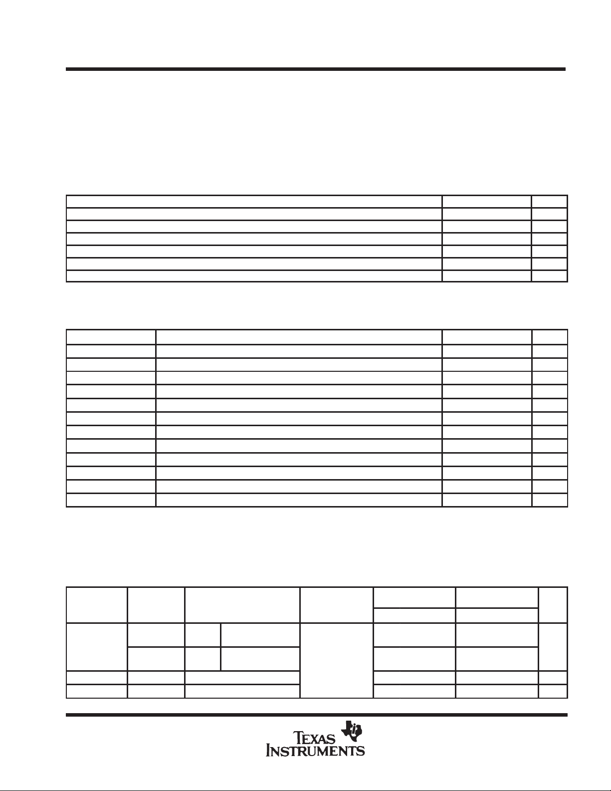
absolute maximum ratings over operating free-air temperature range (unless otherwise noted)
Supply voltage, VCC (see Note 1) 7 V. . . . . . . . . . . . . . . . . . . . . . . . . . . . . . . . . . . . . . . . . . . . . . . . . . . . . . . . . . . .
Input voltage (see Note 1) 5.5 V. . . . . . . . . . . . . . . . . . . . . . . . . . . . . . . . . . . . . . . . . . . . . . . . . . . . . . . . . . . . . . . . . .
Voltage applied to disabled output (see Note 1) 5.5 V. . . . . . . . . . . . . . . . . . . . . . . . . . . . . . . . . . . . . . . . . . . . . . .
Operating free-air temperature range 0°C to 75°C. . . . . . . . . . . . . . . . . . . . . . . . . . . . . . . . . . . . . . . . . . . . . . . . . .
Storage temperature range –65°C to 150°C. . . . . . . . . . . . . . . . . . . . . . . . . . . . . . . . . . . . . . . . . . . . . . . . . . . . . . .
NOTE 1: These ratings apply except for programming pins during a programming cycle or during a preload cycle.
recommended operating conditions
MIN NOM MAX UNIT
V
CC
V
IH
V
IL
I
OH
I
OL
T
A
NOTE 2: These are absolute voltage levels with respect to the ground pin of the device and include all overshoots due to system and/or tester
Supply voltage 4.75 5 5.25 V
High-level input voltage (see Note 2) 2 5.5 V
Low-level input voltage (see Note 2) 0.8 V
High-level output current –3.2 mA
Low-level output current 24 mA
Operating free-air temperature 0 25 75 °C
noise. Testing these parameters should not be attempted without suitable equipment.
CIRCUITS
electrical characteristics over recommended operating free-air temperature range
PARAMETER TEST CONDITIONS MIN TYP†MAX UNIT
V
IK
V
OH
V
OL
‡
I
OZH
‡
I
OZL
I
I
‡
I
IH
‡
I
IL
§
I
OS
I
CC
C
i
C
o
†
All typical values are at VCC = 5 V, TA = 25°C.
‡
I/O leakage is the worst case of I
§
Not more than one output should be shorted at a time, and the duration of the short circuit should not exceed one second. VO is set at 0.5 V to
avoid test problems caused by test equipment ground degradation.
VCC = 4.75 V, II = –18 mA –0.8 –1.5 V
VCC = 4.75 V, IOH = –3.2 mA 2.4 2.7 V
VCC = 4.75 V, IOL = 24 mA 0.3 0.5 V
VCC = 5.25 V, VO = 2.7 V 100 µA
VCC = 5.25 V, VO = 0.4 V –100 µA
VCC = 5.25 V, VI = 5.5 V 100 µA
VCC = 5.25 V, VI = 2.7 V 25 µA
VCC = 5.25 V, VI = 0.4 V –250 µA
VCC = 5.25 V, VO = 0.5 V –30 –70 –130 mA
VCC = 5.25 V, VI = 0, Outputs open 210 mA
f = 1 MHz, VI = 2 V 8.5 pF
f = 1 MHz, VO = 2 V 10 pF
and IIL or I
OZL
and IIH, respectively.
OZH
switching characteristics over recommended ranges of supply voltage and operating free-air
temperature (unless otherwise noted)
FROM
(INPUT)
I, I/O O, I/O
t
pd
t
en
t
dis
I, I/O O, I/O
I, I/O O, I/O 2 7 2 7 ns
I, I/O O, I/O 2 7 2 7 ns
TO
(OUTPUT)
with up to 4 outputs
switching
with more than 4
outputs switching
TEST
CONDITIONS
R1 = 200 Ω,
R2 = 200 Ω,
See Figure 8
TIBPAL20L8-5CFN
MIN MAX MIN MAX
1.5 5 1.5 5
1.5 5 1.5 5.5
TIBPAL20L8-5CJT
TIBPAL20L8-5CNT
UNITPARAMETER
ns
PRODUCTION DATA information is current as of publication date.
Products conform to specifications per the terms of Texas Instruments
standard warranty. Production processing does not necessarily include
testing of all parameters.
POST OFFICE BOX 655303 • DALLAS, TEXAS 75265
9
 Loading...