

Page 1
User's Guide
SBOU161A–February 2016–Revised April 2016
THS3215EVM and THS3217EVM
This user guide describes the characteristics, operation, and use of the THS3215EVM and THS317EVM
(THS321xEVM). This evaluation module (EVM) is a demonstration fixture for the THS3215 andTHS3217
family of wideband, differential DAC to single-ended line drivers. The EVM provides 50-Ω input and output
termination for easy evaluation with common 50-Ω test equipment. A complete circuit description,
schematic diagram, printed circuit board (PCB) layout, and bill of materials are included.
Throughout this document, the terms demonstration kit, evaluation board, evaluation module, and EVM
are synonymous with the THS321xEVM.
All trademarks are the property of their respective owners.
SBOU161A–February 2016–Revised April 2016
Submit Documentation Feedback
Copyright © 2016, Texas Instruments Incorporated
THS3215EVM and THS3217EVM
1
Page 2

www.ti.com
Contents
1 Introduction ................................................................................................................... 3
2 Design Considerations ...................................................................................................... 4
3 Schematic, PCB Layout, and Bill of Materials ........................................................................... 8
List of Figures
1 THS321x Power-Supply Schematic ....................................................................................... 4
2 Logic Control Switches...................................................................................................... 4
3 Midscale Buffer Configuration Options.................................................................................... 5
4 D2S Input Connection Options............................................................................................. 6
5 200-MHz Butterworth Filter Before D2S Inputs.......................................................................... 7
6 OPS Input and Output Connection Options.............................................................................. 8
7 EVM Schematic .............................................................................................................. 9
8 Layer 1: Top Signal Layer................................................................................................. 10
9 Layer 2: GND Plane ....................................................................................................... 10
10 Layer 3: Power Plane, ±V
11 Layer 4: Power Plane, ±V
............................................................................................... 10
CC
............................................................................................... 10
CC
12 Layer 5: GND Plane ....................................................................................................... 11
13 Layer 6: Bottom Signal Layer............................................................................................. 11
List of Tables
1 Bidirectional Switch Settings ............................................................................................... 4
2 Bill of Materials, THS321x EVM ......................................................................................... 13
2
THS3215EVM and THS3217EVM
Copyright © 2016, Texas Instruments Incorporated
SBOU161A–February 2016–Revised April 2016
Submit Documentation Feedback
Page 3

www.ti.com
1 Introduction
This section provides a general description of the THS3215 and THS3217 devices and the EVM.
1.1 THS3215 and THS3217 Description
The THS3215 and THS3217 (THS321x) combine the key signal-chain components required to interface
with a complementary-current output, digital-to-analog converter (DAC). These two-stage devices deliver
the low-distortion, dc-coupled, single-ended signal required by a wide range of applications. The input
stage buffers the DAC resistive termination, and converts the signal from differential to single-ended with a
fixed gain of 2 V/V. The differential to single-ended output is available externally for direct use, and can
also be connected through an RLC filter or attenuator to the input of an internal output power stage (OPS).
The wideband, current-feedback, OPS provides all pins externally for flexible gain setting.
An internal 2 × 1 multiplexer (mux) to the OPS noninverting input provides an easy means to select
between the internal differential-to-single ended stage (D2S) output or an external input. More information
on the THS3215 and THS3217 can be found in their respective product data sheets, SBOS780 and
SBOS766.
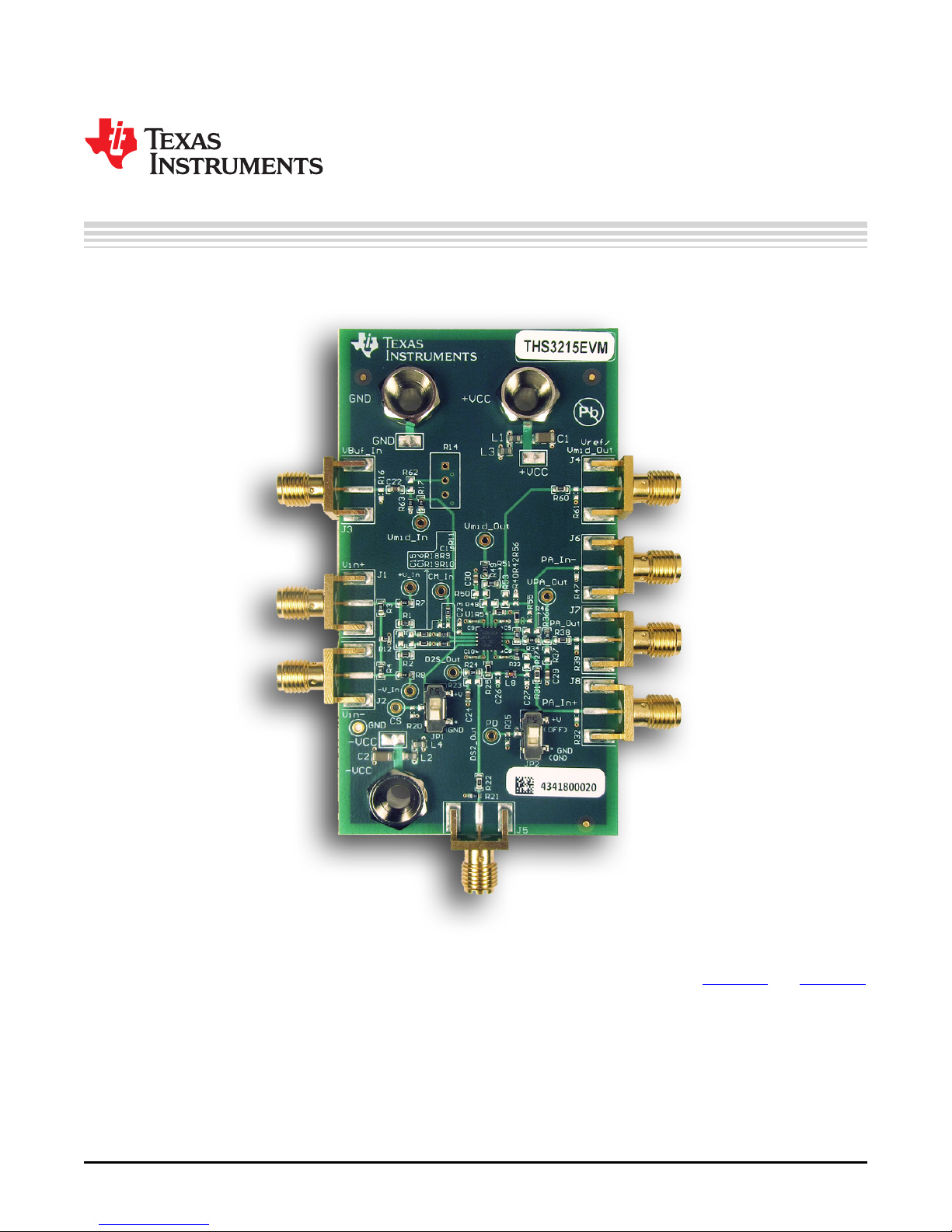
1.2 EVM Description
The THS321xEVM enables performance evaluation of each individual subblock within these devices. The
PCB provides various flexible options to also test either the THS3215 or THS3217 as a complete system.
The EVM provides placeholders to insert filters at different points within the system to allow for more
realistic end-application evaluation.
The following list describes key EVM components:
• Power input: ±6 VDC (typical) at +VCC(P3, TP1) and –VCC(P1, TP2)
• Common reference: GND (P2, TP3 and TP13)
• Interface to the midscale buffer input pin, VMID_IN, through J3 (TP8).
• Interface to the midscale buffer output pin, VMID_OUT, through J4 (TP9).
• Interface to the D2S noninverting signal input pin, IN+, through J1 (TP4).
• Interface to the D2S inverting signal input pin, IN–, through J2 (TP5).
• Interface to the D2S output pin, VO1, through J5 (TP14)
• Interface to the D2S reference input, VREF, through J4. SMA connector J4 is shared with the midscale
buffer output. Depending on the components populated on the board, the appropriate signal is
available at the SMA connector.
• PATHSEL control though switch CS_SW (TP12). Section 2.2 describes the operation of the switch
logic.
• Interface to the OPS external, noninverting input pin, VIN+, through J8.
• DISABLE control though switch PD_SW (TP11). Section 2.2 describes the operation of the switch
logic.
• Interface to the OPS output pin, VOUT, through J7 (TP10).
• Interface to the OPS inverting input pin, VIN–, through J6.
Introduction
SBOU161A–February 2016–Revised April 2016
Submit Documentation Feedback
Copyright © 2016, Texas Instruments Incorporated
THS3215EVM and THS3217EVM
3
Page 4
+Vcc2
TP3
C2
2.2F
L2
L1
L3
L4
1000 ohm
C1
2.2F
C11
0.022F
1000 ohm
GND
TP1
TP2
C4
0.22F
-VCC
+VCC
P 3
P 2
P1
C3
0.22F
C6
0.01F
C5
0.01F
-Vcc1
+Vcc1
C12
0.022F
GND
C7
0.22F
C8
0.22F
C9
0.01F
C10
0.01F
-Vcc2
1000 ohm 1000 ohm
Design Considerations
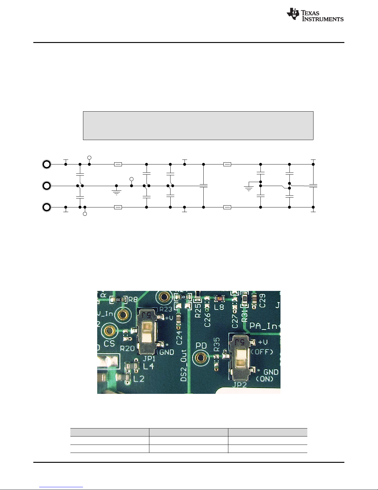
2 Design Considerations
This section discusses general design considerations and options when setting up and configuring the
various blocks in THS321xEVM.
2.1 Power Supplies
Power is applied to the board through connectors P1, P2, and P3, as shown in Figure 1. Both bipolar and
single-sided supplies can be used. The typical supplies are ±6 V.
Supplies beyond ±8.1 V can damage the device.
www.ti.com
CAUTION
2.2 Digital Logic Control
There are two bidirectional switches on the THS321xEVM that control the status of the PATHSEL and
DISABLE control pins. Figure 2 shows the control logic with respect to the switch position. For brevity, the
PATHSEL control is shown as CS and the DISABLE control is shown as PD on the PCB. The full switch
settings are listed in Table 1.
Figure 1. THS321x Power-Supply Schematic
Figure 2. Logic Control Switches
Switch Set to +VCC Set to GND
4
THS3215EVM and THS3217EVM
CS_SW (PATHSEL control) OPS external, noninverting path Internal path from D2S to OPS
PD_SW (DISABLE control) OPS off OPS on
SBOU161A–February 2016–Revised April 2016
Table 1. Bidirectional Switch Settings
Copyright © 2016, Texas Instruments Incorporated
Submit Documentation Feedback
Page 5

+Vcc2 -Vcc1
Junc Vneg
Junc Vocm
GND
GND
GND
GND
GND
+Vcc1+Vcc2
GND Junc Vneg
Junc Vocm
GND
GND
GND
-Vcc2 -Vcc1
VBuf_In
Vref/Vmid_Out
PA_In-
PA_Out
TP7
DNP
CM_In
TP8
DNP
Vmid_In
TP9
DNP
Vmid_Out
TP10
DNP
VPA_Out
0.22µF
C29
0.22µF
C19
DNP
0.22µF
C22
0.22µF
C30
49.9
R33
49.9
R34
49.9
R51
49.9
R6349.9
R16
DNP
10.0k
R17
10.0k
R49
10.0k
R5
DNP
10.0k
R6
DNP
10.0
R9
10.0
R10
10.0
R11
1.00k
R13
1.00k
R15
1k
R14
DNP
0
R54
0
R60
0
R56
DNP
0
R55
DNP
0
R53
DNP
0
R48
DNP
0
R38
20k
R36
249
R40
162
R42
0.01µF
C23
DNP
1.00
R37
DNP
1.00
R50
DNP
75.0
R47
DNP
56.2
R39
DNP
56.2
R61
DNP
150
R46
DNP
4.02k
R62
DNP
DISABLE
10
GND
7
+IN
2
-IN
3
PAD
17
PATHSEL
4
VIN-
12
+VCC2
16
+VCC1
13
-VCC1
8
-VCC2
5
VIN+
9
VMID_IN
1
VMID_OUT
15
VO1
6
VOUT
11
VREF
14
U1
1
234
5
J3
1
234
5
J4
1
234
5
J6
1
234
5
J7
THS3215IRGVR
Or
THS3217IRGVR
www.ti.com
2.3 Midscale or Reference Buffer
The EVM is configured by default to drive a ground-centered signal. In cases where a different output
common-mode voltage is required, use the midscale buffer to provide a low impedance path. This buffer is
also used in applications where a servo loop is required to set the dc offset of the system to a desired
value. Alternatively, the buffer can also be used to set the reference voltage in single-supply applications
where the inputs to the D2S are ac-coupled. The midscale buffer input defaults to the midsupply voltage.
In cases where a different input voltage is required, adjust the R14 potentiometer (uninstalled by default)
to achieve the desired offset voltage. Resistor R62 must be appropriately sized, and resistor R63
uninstalled in order to set the correct voltage at the input of the midscale buffer. The EVM allows for
connecting the output of the midscale buffer to various nodes of the THS321x. The different options are:
1. In single-supply and ac-coupled applications, the common-mode input of the D2S is configured in one
of two ways. The first way is by installing R56 = 0 Ω. This setting connects the output of the buffer to
the Junc_Vocm node on the board. Components R5, R6, R11, and C19 must be appropriately sized
and installed. The second way is by applying an external common-mode voltage through test-point
TP7.
2. If the output common-mode voltage of the D2S must be set to any voltage other than GND, uninstall
resistors R54 and R51, and install R48 instead. This configuration connects the output of the midscale
buffer to VREF (pin 14).
3. If the OPS is configured in the noninverting mode with a common-mode dc offset voltage from the
D2S, then the D2S provides the necessary dc bias to the noninverting pin of the OPS. However, if the
OPS RGis grounded, the dc common-mode offset voltage from the D2S is amplified by (1 + RF/ RG),
and may result in limited output headroom from the OPS. To prevent this limitation, connect RGto the
midscale buffer output so that the common-mode gain is 0 dB by setting R55 to the desired value of
the gain resistor and uninstalling R42. Installing R55 connects the output of the midscale buffer to
Junc_Vneg enabling configuration of the OPS in a level-shifted, common-mode, noninverting
configuration. Make sure that R54 and R60 are uninstalled, and R51 = R53 = 0 Ω in this configuration.
The areas within the dashed boxes in Figure 3 show the described configurations.
Design Considerations
SBOU161A–February 2016–Revised April 2016
Submit Documentation Feedback
Figure 3. Midscale Buffer Configuration Options
Copyright © 2016, Texas Instruments Incorporated
THS3215EVM and THS3217EVM
5
Page 6

+Vcc2 -Vcc1
GND
GND
+Vcc1+Vcc2
TP4
DNP
GND
Junc Vocm
GND
GND
-Vcc2 -Vcc1
GNDGND
GND
Vin+
Vin-
VBuf_In
D2S_Out
TP5
DNP
+V_In
-V_In
TP7
DNP
CM_In
TP8
DNP
Vmid_In
TP14
DNP
D2S_Out
GND
0.22µF
C15
DNP
0.22µF
C16
DNP
0.22µF
C19
DNP
0.22µF
C22
0.22µF
C24
49.9
R3
49.9
R4
49.9
R33
49.9
R6349.9
R16
DNP
10.0k
R8
10.0k
R7
10.0k
R17
10.0k
R5
DNP
10.0k
R6
DNP
10.0
R9
10.0
R10
10.0
R11
1.00k
R13
1.00k
R15
1k
R14
DNP
73.2
R21
0
R22
0
R27
DNP
20k
R24
169
R25
0.01µF
C23
DNP
2.2pF
C26
DNP
11pF
C27
DNP
1.00
R23
DNP
4.02k
R62
DNP
DISABLE
10
GND
7
+IN
2
-IN
3
PAD
17
PATHSEL
4
VIN-
12
+VCC2
16
+VCC1
13
-VCC1
8
-VCC2
5
VIN+
9
VMID_IN
1
VMID_OUT
15
VO1
6
VOUT
11
VREF
14
U1
THS3215IRGVR
Or
THS3217IRGVR
72nH
L8
DNP
0
R1
0
R2
0
R18
0
R19
0
R12
1
234
5
J3
1
234
5
J1
1
234
5
J2
1
234
5
J5
Uninstall all the RLC filter components if
not used in the application to prevent
loading the D2S output
Design Considerations
2.4 Differential to Single-Ended Stage (D2S)
The D2S inputs are driven by an external differential signal through SMA connectors J1 and J2. Standard
lab equipment usually provides only a single-ended output. The LMH3401, a very wideband, single-ended
to differential amplifier, was used during product evaluation to drive a differential signal into the D2S. The
spacing of the SMA connectors on the THS321xEVM is designed to interface directly with the output of
the LMH3401EVM through standard SMA barrel connectors. The THS321xEVM provides a standard 100Ω differentially-terminated resistive network to GND, dc-coupled to the D2S input pins. Figure 4 shows the
EVM schematic of the D2S input/output network with the default passive components installed. The output
of the D2S can also be measured externally at J5.
www.ti.com
Figure 4. D2S Input Connection Options
6
THS3215EVM and THS3217EVM
Copyright © 2016, Texas Instruments Incorporated
SBOU161A–February 2016–Revised April 2016
Submit Documentation Feedback
Page 7

2
3
49.9
IN±
IN+
10 mA
10 mA
I
DIFF
Complementary
Output DAC
15 pF
72 nH
49.9 14.4 pF
15 pF
49.9
14.4 pF
D2S Input
72 nH
49.9
www.ti.com
The EVM allows for flexibility in the D2S input network configuration. The different options are:
1. In order to reduce the high-frequency noise and distortion components from the previous stage driving
Design Considerations
the D2S, a passive RLC filter can be inserted prior to the D2S inputs. Figure 5 shows an example of a
third-order, 200-MHz, Butterworth filter placed between the DAC output and D2S input. The
THS321xEVM is able to evaluate system performance with similar RLC-filter architectures installed on
the board.
Figure 5. 200-MHz Butterworth Filter Before D2S Inputs
2. In single-supply and ac-coupled applications, use R18 and R19 to install the appropriately-sized, acblocking capacitors (see Figure 4). Use the midscale buffer output in conjunction with R56, R11, R5,
and R6 to set the desired dc common-mode voltage for the D2S input.
3. The output of the D2S is fed into the internal, noninverting input pin of the OPS by driving PATHSEL
low through switch CS_SW.
4. Certain applications may require an interstage filter inserted between the D2S and OPS to reduce
overall system noise, and prevent high-frequency harmonics from previous stages propagating to the
OPS output. In such situations, use C26, L8, and C27 to insert a third-order, RLC filter into the signal
path of the THS321x (see Figure 4). The output of the filter then drives the external noninverting input
of the OPS, VIN+ (pin 9).
SBOU161A–February 2016–Revised April 2016
Submit Documentation Feedback
Copyright © 2016, Texas Instruments Incorporated
THS3215EVM and THS3217EVM
7
Page 8

GND
GND
+Vcc1+Vcc2
Junc Vneg
GND
GND
-Vcc2 -Vcc1
GND
PA_In-
PA_Out
PA_In+
TP10
DNP
VPA_Out
0.22 µF
C29
49.9
R33
49.9
R34
0
R31
0
R27
DNP
0
R38
20k
R36
169
R25
249
R40
162
R42
2.2pF
C26
DNP
11pF
C27
DNP
1.00
R37
DNP
75.0
R32
DNP
75.0
R47
DNP
56.2
R39
DNP
150
R46
DNP
DISABLE
10
GND
7
+IN
2
-IN
3
PAD
17
PATHSEL
4
VIN-
12
+VCC2
16
+VCC1
13
-VCC1
8
-VCC2
5
VIN+
9
VMID_IN
1
VMID_OUT
15
VO1
6
VOUT
11
VREF
14
U1
THS3217IRGVR
72nH
L8
DNP
1
234
5
J6
1
234
5
J7
1
234
5
J8
THS3215IRGVR
Or
THS3217IRGVR
Uninstall the RLC filter when configuring the
OPS as a standalone amplifier
Design Considerations
2.5 Output Power Stage (OPS)
As described in option 3 and option 4 of Section 2.4, the OPS can be driven internally or externally. The
OPS can be also used as a standalone amplifier in an inverting or noninverting configuration. The output
of the OPS is available at SMA connector J7. Figure 6 shows the EVM schematic of the OPS input/output
network with the default passive components installed. The different options are:
1. When configuring the OPS as a standalone-noninverting amplifier, apply the external input at J8. Set
termination resistor R33 = 49.9 Ω.
2. When configuring the OPS as a standalone-inverting amplifier, apply the external input at J6. Set R46
as the RGresistor, and R47 as the termination resistor. R42 must be uninstalled in this configuration.
3. To conserve power, disable the OPS by setting the DISABLE control low through switch PD_SW.
www.ti.com
Figure 6. OPS Input and Output Connection Options
3 Schematic, PCB Layout, and Bill of Materials
This section provides a complete schematic diagram, PCB layout, and bill of materials (BOM) for the
THS321xEVM.
3.1 Schematic
Figure 7 shows the schematic.
8
THS3215EVM and THS3217EVM
Copyright © 2016, Texas Instruments Incorporated
SBOU161A–February 2016–Revised April 2016
Submit Documentation Feedback
Page 9

www.ti.com
Schematic, PCB Layout, and Bill of Materials
9
SBOU161A–February 2016 –Revised April 2016
Submit Documentation Feedback
Copyright © 2016, Texas Instruments Incorporated
THS3215EVM and THS3217EVM
Figure 7. EVM Schematic
Page 10

Schematic, PCB Layout, and Bill of Materials
3.2 PCB Layout
The PCB layers are shown in Figure 8 through Figure 13.
www.ti.com
Figure 8. Layer 1: Top Signal Layer Figure 9. Layer 2: GND Plane
10
THS3215EVM and THS3217EVM
Copyright © 2016, Texas Instruments Incorporated
SBOU161A–February 2016–Revised April 2016
Submit Documentation Feedback
Page 11

www.ti.com
Schematic, PCB Layout, and Bill of Materials
Figure 10. Layer 3: Power Plane, ±V
SBOU161A–February 2016–Revised April 2016
Submit Documentation Feedback
CC
Copyright © 2016, Texas Instruments Incorporated
Figure 11. Layer 4: Power Plane, ±V
CC
THS3215EVM and THS3217EVM
11
Page 12

Schematic, PCB Layout, and Bill of Materials
www.ti.com
Figure 12. Layer 5: GND Plane Figure 13. Layer 6: Bottom Signal Layer
12
THS3215EVM and THS3217EVM
Copyright © 2016, Texas Instruments Incorporated
SBOU161A–February 2016–Revised April 2016
Submit Documentation Feedback
Page 13

www.ti.com
3.3 Bill of Materials
Table 2 lists the bill of materials for the THS321xEVM. The BOMs for the THS3215EVM and
THS3217EVM are identical except for the line item corresponding to the DUT model populated on the
EVM.
Schematic, PCB Layout, and Bill of Materials
Table 2. Bill of Materials, THS321x EVM
Item #
1 C1, C2 2 GRM31MR71E225KA93L MuRata CAP, CERM, 2.2 µF, 25 V, +/- 10%, X7R, 1206
2 C3, C4, C7, C8,
3 C5, C6, C9, C10 4 GRM155R71E103KA01D MuRata CAP, CERM, 0.01 µF, 25 V, +/- 10%, X7R, 0402
4 C11, C12 2 250X14W223MV4T Johanson Technology CAP, CERM, 0.022 µF, 25 V, +/- 20%, X7R, 0603
5 J1, J2, J3, J4, J5,
6 JP1, JP2 2 CL-SB-12B-01T Copal Electronics Switch, Slide, SPDT, 0.2A, GULL, 12V, SMD
7 L1, L2, L3, L4 4 BLM21AG102SN1D MuRata Ferrite Bead, 1000 ohm @ 100 MHz, 0.5 A, 0805
8 L8 1 AISC-0603HP-72NJ-T Abracon Corporation Inductor, Wirewound, 72 nH, 0.58 A, 0.35 ohm, SMD
9 P1, P2, P3 3 6095 Keystone Standard Banana Jack, Uninsulated
10 R1, R2, R12, R18,
11 R3, R4, R33, R34,
12 R5, R6, R7, R8,
13 R9, R10, R11 3 RC0603FR-0710RL Yageo America RES, 10.0, 1%, 0.1 W, 0603
14 R13, R15 2 ERJ-3EKF1001V Panasonic RES, 1.00 k, 1%, 0.1 W, 0603
15 R21 1 CRCW060373R2FKEA Vishay-Dale RES, 73.2, 1%, 0.1 W, 0603
16 R24, R36 2 CRCW060320K0JNEA Vishay-Dale RES, 20 k, 5%, 0.1 W, 0603
17 R25 1 CRCW0603169RFKEA Vishay-Dale RES, 169, 1%, 0.1 W, 0603
18 R40 1 CRCW0603249RFKEA Vishay-Dale RES, 249, 1%, 0.1 W, 0603
19 R42 1 CRCW0603162RFKEA Vishay-Dale RES, 162, 1%, 0.1 W, 0603
20 U1 1 THS3215IRGVR OR
21 C15, C16, C19 0 GRM188R71E224KA88D MuRata CAP, CERM, 0.22 µF, 25 V, +/- 10%, X7R, 0603
22 C23 0 GRM188R71E103KA01D MuRata CAP, CERM, 0.01 µF, 25 V, +/- 10%, X7R, 0603
23 C26 0 06035A2R2CAT2A AVX CAP, CERM, 2.2 pF, 50 V, +/- 11%, C0G/NP0, 0603
24 C27 0 GRM1885C1H110JA01D MuRata CAP, CERM, 11 pF, 50 V, +/- 5%, C0G/NP0, 0603
25 R14 0 3296W-1-102LF Bourns TRIMMER, 1k ohm, 0.5W, TH
26 R16, R20, R35 0 ERJ-3EKF49R9V Panasonic RES, 49.9, 1%, 0.1 W, AEC-Q200 Grade 0, 0603
27 R23, R37, R50 0 CRCW06031R00FKEA Vishay-Dale RES, 1.00, 1%, 0.1 W, 0603
28 R27, R48, R53,
29 R32, R47 0 CRCW060375R0FKEA Vishay-Dale RES, 75.0, 1%, 0.1 W, 0603
30 R39, R61 0 RC0603FR-0756R2L Yageo America RES, 56.2, 1%, 0.1 W, 0603
31 R46 0 RC0603FR-07150RL Yageo America RES, 150, 1%, 0.1 W, 0603
32 R62 0 RC0603FR-074K02L Yageo America RES, 4.02 k, 1%, 0.1 W, 0603
33 TP1, TP2, TP3 0 5019 Keystone Test Point, Miniature, SMT
34 TP4, TP5, TP7,
Reference
Designator Quantity Part Number Value Description
C22, C24, C29, C30
J6, J7, J8
R19, R22, R31,
R38, R54, R60
R51, R63
R17, R49
R55, R56
TP8, TP9, TP10,
TP11, TP12, TP13,
TP14
8 GRM188R71E224KA88D MuRata CAP, CERM, 0.22 µF, 25 V, +/- 10%, X7R, 0603
8 142-0701-851 Emerson Network
Power
10 ERJ-3GEY0R00V Panasonic RES, 0, 5%, 0.1 W, 0603
6 ERJ-3EKF49R9V Panasonic RES, 49.9, 1%, 0.1 W, AEC-Q200 Grade 0, 0603
6 ERJ-3EKF1002V Panasonic RES, 10.0 k, 1%, 0.1 W, 0603
Texas Instruments Wideband Differential DAC to Single Ended Line
THS3217IRGVR
0 ERJ-3GEY0R00V Panasonic RES, 0, 5%, 0.1 W, 0603
0 5003 Keystone Test Point, Miniature, Orange, TH
Connector, End launch SMA, 50 ohm, SMT
Driver, RGV0016A
SBOU161A–February 2016–Revised April 2016
Submit Documentation Feedback
Copyright © 2016, Texas Instruments Incorporated
THS3215EVM and THS3217EVM
13
Page 14

Revision History
www.ti.com
Revision History
NOTE: Page numbers for previous revisions may differ from page numbers in the current version.
Changes from Original (February 2016) to A Revision .................................................................................................. Page
• Added THS3215EVM and related information to this user's guide................................................................. 1
• Changed front page EVM photo......................................................................................................... 1
• Changed Figure 3 to match new Figure 7 schematic ................................................................................ 5
• Changed Figure 4 to match new Figure 7 schematic ................................................................................ 6
• Changed Figure 7......................................................................................................................... 9
• Changed PCB layout, Figure 8 to Figure 13 ......................................................................................... 10
• Changed BOM ........................................................................................................................... 13
14
Revision History
Copyright © 2016, Texas Instruments Incorporated
SBOU161A–February 2016–Revised April 2016
Submit Documentation Feedback
Page 15

IMPORTANT NOTICE
Texas Instruments Incorporated and its subsidiaries (TI) reserve the right to make corrections, enhancements, improvements and other
changes to its semiconductor products and services per JESD46, latest issue, and to discontinue any product or service per JESD48, latest
issue. Buyers should obtain the latest relevant information before placing orders and should verify that such information is current and
complete. All semiconductor products (also referred to herein as “components”) are sold subject to TI’s terms and conditions of sale
supplied at the time of order acknowledgment.
TI warrants performance of its components to the specifications applicable at the time of sale, in accordance with the warranty in TI’s terms
and conditions of sale of semiconductor products. Testing and other quality control techniques are used to the extent TI deems necessary
to support this warranty. Except where mandated by applicable law, testing of all parameters of each component is not necessarily
performed.
TI assumes no liability for applications assistance or the design of Buyers’ products. Buyers are responsible for their products and
applications using TI components. To minimize the risks associated with Buyers’ products and applications, Buyers should provide
adequate design and operating safeguards.
TI does not warrant or represent that any license, either express or implied, is granted under any patent right, copyright, mask work right, or
other intellectual property right relating to any combination, machine, or process in which TI components or services are used. Information
published by TI regarding third-party products or services does not constitute a license to use such products or services or a warranty or
endorsement thereof. Use of such information may require a license from a third party under the patents or other intellectual property of the
third party, or a license from TI under the patents or other intellectual property of TI.
Reproduction of significant portions of TI information in TI data books or data sheets is permissible only if reproduction is without alteration
and is accompanied by all associated warranties, conditions, limitations, and notices. TI is not responsible or liable for such altered
documentation. Information of third parties may be subject to additional restrictions.
Resale of TI components or services with statements different from or beyond the parameters stated by TI for that component or service
voids all express and any implied warranties for the associated TI component or service and is an unfair and deceptive business practice.
TI is not responsible or liable for any such statements.
Buyer acknowledges and agrees that it is solely responsible for compliance with all legal, regulatory and safety-related requirements
concerning its products, and any use of TI components in its applications, notwithstanding any applications-related information or support
that may be provided by TI. Buyer represents and agrees that it has all the necessary expertise to create and implement safeguards which
anticipate dangerous consequences of failures, monitor failures and their consequences, lessen the likelihood of failures that might cause
harm and take appropriate remedial actions. Buyer will fully indemnify TI and its representatives against any damages arising out of the use
of any TI components in safety-critical applications.
In some cases, TI components may be promoted specifically to facilitate safety-related applications. With such components, TI’s goal is to
help enable customers to design and create their own end-product solutions that meet applicable functional safety standards and
requirements. Nonetheless, such components are subject to these terms.
No TI components are authorized for use in FDA Class III (or similar life-critical medical equipment) unless authorized officers of the parties
have executed a special agreement specifically governing such use.
Only those TI components which TI has specifically designated as military grade or “enhanced plastic” are designed and intended for use in
military/aerospace applications or environments. Buyer acknowledges and agrees that any military or aerospace use of TI components
which have not been so designated is solely at the Buyer's risk, and that Buyer is solely responsible for compliance with all legal and
regulatory requirements in connection with such use.
TI has specifically designated certain components as meeting ISO/TS16949 requirements, mainly for automotive use. In any case of use of
non-designated products, TI will not be responsible for any failure to meet ISO/TS16949.
Products Applications
Audio www.ti.com/audio Automotive and Transportation www.ti.com/automotive
Amplifiers amplifier.ti.com Communications and Telecom www.ti.com/communications
Data Converters dataconverter.ti.com Computers and Peripherals www.ti.com/computers
DLP® Products www.dlp.com Consumer Electronics www.ti.com/consumer-apps
DSP dsp.ti.com Energy and Lighting www.ti.com/energy
Clocks and Timers www.ti.com/clocks Industrial www.ti.com/industrial
Interface interface.ti.com Medical www.ti.com/medical
Logic logic.ti.com Security www.ti.com/security
Power Mgmt power.ti.com Space, Avionics and Defense www.ti.com/space-avionics-defense
Microcontrollers microcontroller.ti.com Video and Imaging www.ti.com/video
RFID www.ti-rfid.com
OMAP Applications Processors www.ti.com/omap TI E2E Community e2e.ti.com
Wireless Connectivity www.ti.com/wirelessconnectivity
Mailing Address: Texas Instruments, Post Office Box 655303, Dallas, Texas 75265
Copyright © 2016, Texas Instruments Incorporated
 Loading...