
TCM4400E
GSM/DCS BASEBAND AND VOICE A/D
AND D/A RF INTERFACE CIRCUIT
SLWS082A – JULY 1999 – REVISED MARCH 2000
1
POST OFFICE BOX 655303 • DALLAS, TEXAS 75265
D
Applications Include GSM 900,
PCS 1900, and DCS 1800 Cellular
Telephones
D
80-Pin TQFP (0.4 mm or 0.5 mm Lead
Pitch) or 80-Ball MicroStar BGA
Packages
D
Single 3-V Supply Voltage
D
Internal Voltage Reference
D
Extended RF Control Voltages
D
Advanced Power Management
D
GSM-Digital Audio Interface (DAI)
D
MCU and DSP Serial Interface
D
Five Ports Auxiliary A/D
D
Meets JTAG Testability Standard (IEEE
Std 1131.1-1990)
D
Baseband Codec-GMSK Modulator
With On-Chip Burst Buffer
D
Voice Codec Features: Microphone
Amplifier and Bias Source,
Programmable Gain Amplifiers, Volume
Control, and Side-Tone Control
description
The TCM4400E global system for mobile communication (GSM) baseband RF interface circuit is designed for
GSM 900 , PCS1900, and DCS 1800 European digital cellular telecommunication systems. It performs the
interface and processing of voice signals, generates baseband in-phase (I) and quadrature (Q) signals, and
controls the signals between a digital signal processor (DSP) and associated RF circuits.
The TCM4400E includes a second serial interface for use with a microcontroller. Through this interface, a
microcontroller can access all the internal registers that can be accessed through the DSP digital serial
interface. This option is intended for applications in which part of the L1 software is implemented in the
microcontroller.
A four-pin parallel port is dedicated to the full control of the digital audio interface (DAI) to the GSM system
simulator; the DAI consists of system simulator reset (SSRST) control, clock generation, and rate adaptation
with the DSP.
The voice processing portion of the device includes microphone and earphone amplifiers, analog-to-digital
(A/D) and digital-to-analog (D/A) converters, speech digital filtering, and a serial port.
The baseband processing portion of the device includes a two-channel uplink path, a two-channel downlink
path, a serial port, and a parallel port. The uplink path performs Gaussian minimum shift keying (GMSK)
modulation and D/A conversion, and it has smoothing filters to provide the external RF circuit with I and Q
baseband signals. The downlink path performs antialiasing, A/D conversion, and channel separation filtering
of the baseband I and Q signals. The serial port allows baseband data exchange with the DSP , and the parallel
port controls precise timing signals.
Auxiliary RF functions such as automatic frequency control (AFC), automatic gain control (AGC), power control,
and analog monitoring are also implemented in the TCM4400E. Internal functional blocks of the device can be
separately and automatically powered down with GSM RF windows.
These devices have limited built-in ESD protection. The leads should be shorted together or the device placed in conductive foam
during storage or handling to prevent electrostatic damage to the MOS gates.
Please be aware that an important notice concerning availability, standard warranty, and use in critical applications of
Texas Instruments semiconductor products and disclaimers thereto appears at the end of this data sheet.
Copyright 2000, Texas Instruments Incorporated
PRODUCTION DATA information is current as of publication date.
Products conform to specifications per the terms of Texas Instruments
standard warranty. Production processing does not necessarily include
testing of all parameters.
MicroStar BGA is a trademark of Texas Instruments.

TCM4400E
GSM/DCS BASEBAND AND VOICE A/D
AND D/A RF INTERFACE CIRCUIT
SLWS082A – JULY 1999 – REVISED MARCH 2000
2
POST OFFICE BOX 655303 • DALLAS, TEXAS 75265
22 23
BULIP
BULIN
BULQP
BULQN
AV
DD2
AV
SS2
BDLIN
BDLIP
BDLQN
BDLQP
VMID
DV
SS3
AV
SS3
APC
AFC
AGC
ADCMID
AV
DD5
DV
DD3
AV
DD3
60
59
58
57
56
55
54
53
52
51
50
49
48
47
46
45
44
43
42
41
24
1
2
3
4
5
6
7
8
9
10
11
12
13
14
15
16
17
18
19
20
BFSX
BCLKX
BDX
BDR
BCLKR
BFSR
AV
DD1
V
REF
IBIAS
VGAP
AV
SS1
RESET
VFS
VDX
VDR
VCLK
SSRST
SSDX
SSDR
SSCLK
25 26 27 28
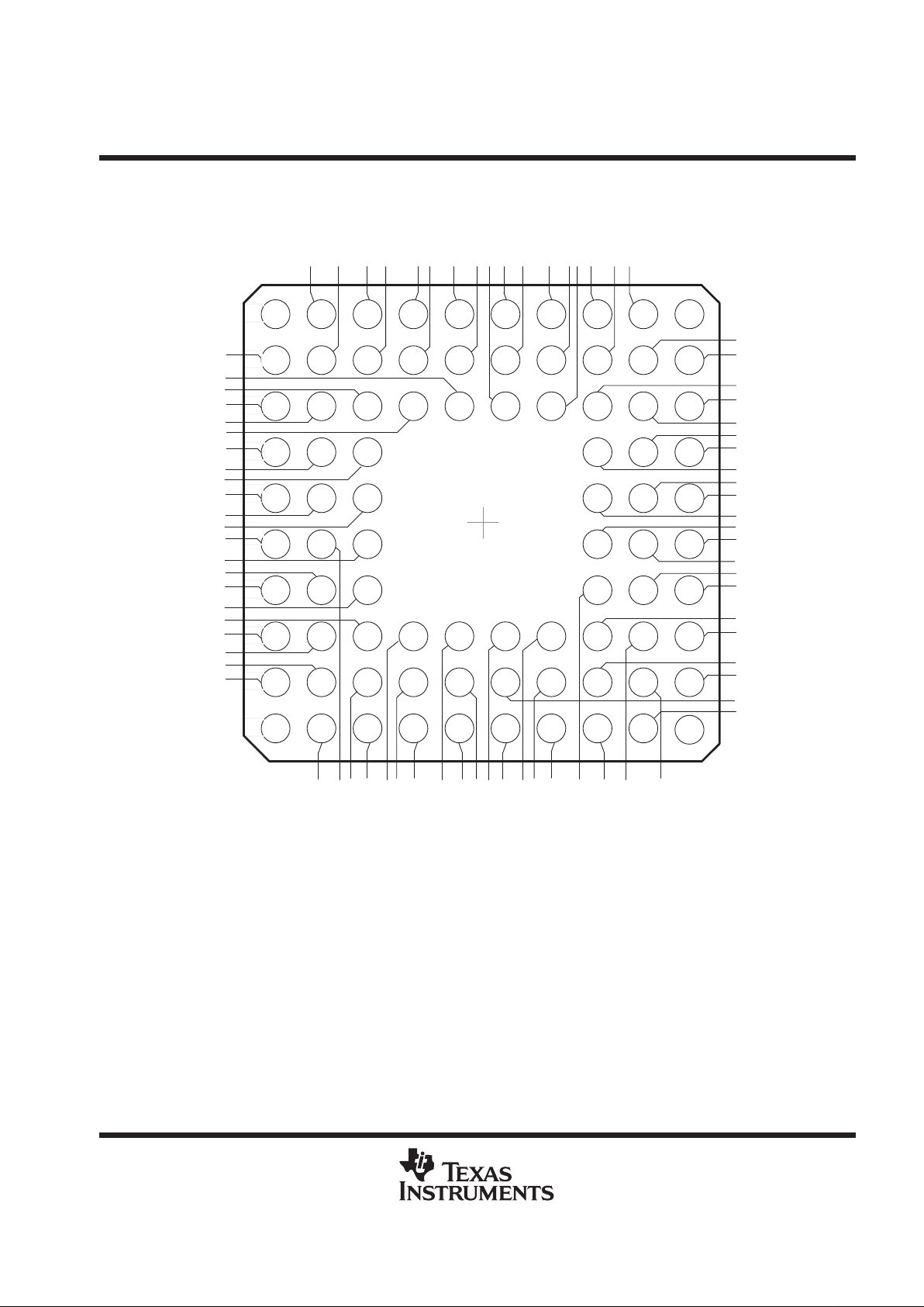
80-Pin TQFP PACKAGE
(TOP VIEW)
MCLK
79 78 77 76 7580 74
UCLK
UDR
UDX
USEL
BDLON
BULON
BCAL
PWRDN
TRST
GNDA1
MICBIAS
MICIP
MICIN
72 71 7073
29
30 31 32 33
69 68
21
TEST2
67 66 65 64
34 35 36 37
AUXO
GNDA2
TEST3
TCK
ADIN4
38 39 40
TDI
TDO
63 62 61
TEST1
TMS
EARP
ADIN5
DV
DD4
DV
SS4
AV
SS4
DV
DD1DVSS1
BENA
DV
DD2
DV
SS2
AUXI
AV
DD4
EARN
ADIN1
ADIN2
ADIN3
TCM4400E
GSM/DCS BASEBAND AND VOICE A/D
AND D/A RF INTERFACE CIRCUIT
SLWS082A – JULY 1999 – REVISED MARCH 2000
3
POST OFFICE BOX 655303 • DALLAS, TEXAS 75265
109876532 41
J
H
G
F
K
E
D
A
B
C
ADCMID
ADIN1
ADIN2
ADIN3
ADIN4
ADIN5
AFC
AGC
APC
AUXI
AUXO
AV
DD1
AV
DD2
AV
DD3
AV
DD4
AV
DD5
AV
SS1
AV
SS2
AV
SS3
AV
SS4
BCAL
BDR
BDX
BENA
BDLON
BFSR
BFSX
BDLIN
BDLIP
BDLQN
BDLQP
BULIN
BULIP
BULON
BULQN
DV
DD1
DV
DD2
DV
DD3
DV
DD4
DV
SS1
DV
SS2
DV
SS3
DV
SS4
EARN
EARP
GNDA1
GNDA2
IBIAS
TEST1
MICBIAS
MICIP
MICIN
PWRDN
RESET
SSCLK
SSDR
SSDX
SSRST
TCK
TDI
TDO
TEST3
TEST2
MCLK
TMS
TRST
UCLK
UDR
UDX
VCLK
VDR
VDX
VFS
VGAP
VMID
V
REF
NC
NCNC
BCLKX
NC
BULQP
USEL
BCLKR
NC – No internal connection
GGM PACKAGE
(TOP VIEW)
B1 B2
A2 A3
D1 D2 D3 D8 D9 D10
K2 K3 K4 K5 K6 K7 K8 K9
J1
F1
E1
C1
H2
G2F2G3
F3
C2 C3
B3
C4 C5 C6 C7 C8 C9
C10
B10
A4 A5 A6 A7 A8 A9
E8 E9 E10
J10
H10
G8 G9 G10
F8 F9 F10
H1
G1
J2 J3 J4 J5 J6 J7 J8 J9
H3 H4 H5 H6 H7 H8 H9
E2 E3
B4 B5 B6 B7 B8 B9
TCM4400E
GSM/DCS BASEBAND AND VOICE A/D
AND D/A RF INTERFACE CIRCUIT
SLWS082A – JULY 1999 – REVISED MARCH 2000
4
POST OFFICE BOX 655303 • DALLAS, TEXAS 75265
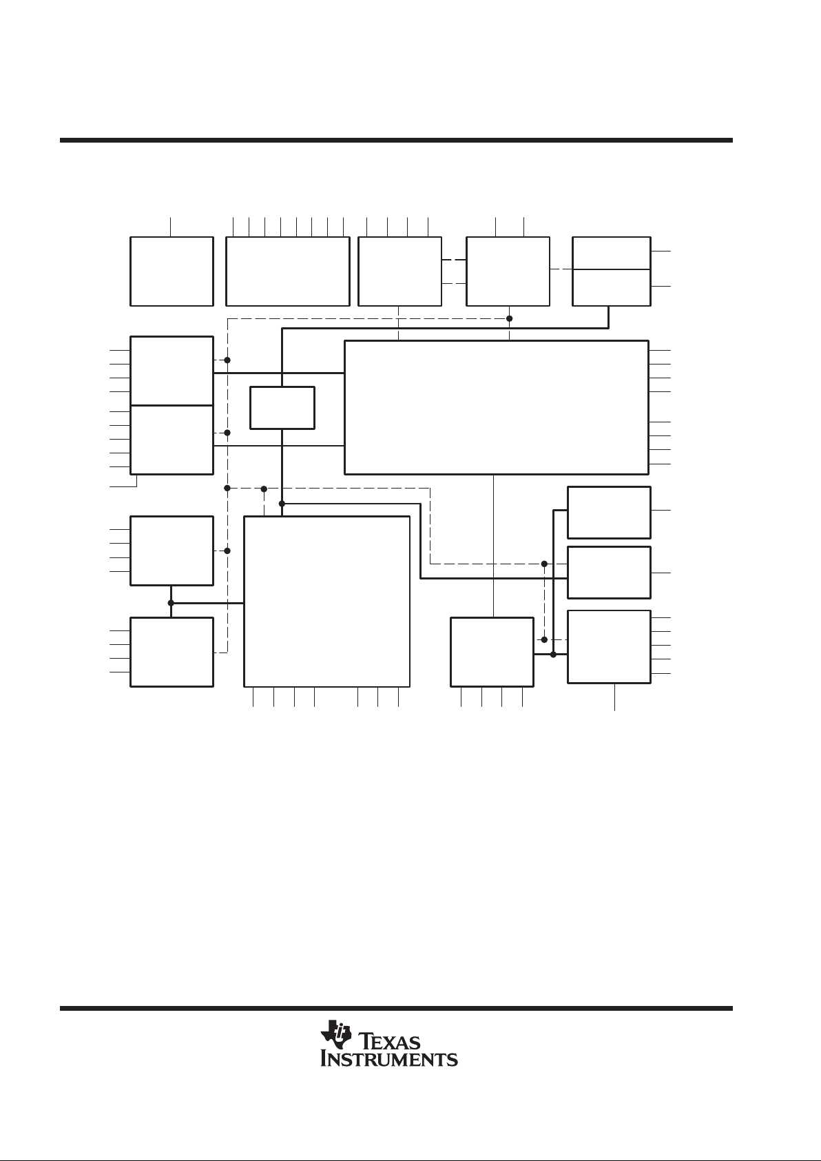
functional block diagram
USEL
Main Clock
Generator
GSM Windows
Timing
Interface
JTAG
Interface
Power
Management
Bus
Controller
Auxiliary DAC
Analog AGC
APC (D/A)
RF TX Ramp
MCU
Serial
Interface
DSP
Serial
Interface
Voiceband
Serial
Interface
DAI
Interface
Voice Uplink 13 Bit ADC
Two Analog Inputs
Programmable Gain
Bandpass Digital Filter
Side-tone
Baseband Uplink GMSK Modulator
Internal Burst RAM
Automatic Offset Compensation
8-Bit DAC and Smoothing Filter
Baseband Downlink I/Q Path
Automatic Offset Compensation
10-Bit ADC and Antialiasing Filter
AGC, AFC
APC Output
Swing Control
Voice Downlink 13 Bit DAC
Auxiliary Earphone Output
Programmable Volume
Smoothing Filter
Bandpass Digital Filter
I
REF-VREF
VMID
Bias
AFC (D/A)
VTCXO Control
Auxiliary
10 Bits
5 Inputs ADC
MICBIAS
MICIN
AUXI
MICIP
EARP
EARN
AUXO
MCLK
AGC
TRST
TDO
TDI
TCK
BENA
BCAL
BDLON
BULON
PWRDN
APC
BULIP
BULIN
BULQN
BULQP
BDLIP
BDLIN
BDLQN
BDLQP
AV
DD5
AFC
ADIN1
ADIN2
ADIN3
ADIN4
ADIN5
IBIAS
VREF
VMID
VGAP
UCLK
UDX
UDR
BFSX
BDX
BCLKX
BFSR
BDR
BCLKR
VCLK
VFS
VDX
VDR
SSCLK
SSRST
SSDX
SSDR
TMS
75
78
76
77
1
3
2
6
4
5
16
13
14
15
20
17
18
19
TEST1
TEST2
TEST3
RESET
70
246263
64
71
72
74
73
23
61
696867
12
45
47
60
59
57
58
53
54
52
51
43
46
36
37
38
39
40
26
28
29
27
32
33
34
9
8
50
10
ADCMID
44

TCM4400E
GSM/DCS BASEBAND AND VOICE A/D
AND D/A RF INTERFACE CIRCUIT
SLWS082A – JULY 1999 – REVISED MARCH 2000
5
POST OFFICE BOX 655303 • DALLAS, TEXAS 75265
Terminal Functions
TERMINAL
NO.
I/O DESCRIPTION
NAME
QFP BGA
ADCMID 44 H8 I/O Reference voltage of auxiliary A/D converters; decoupling only (analog)
ADIN1 36 J7 I Auxiliary 10-bit ADC input 1 (analog)
ADIN2 37 H7 I Auxiliary 10-bit ADC input 2 (analog)
ADIN3 38 K8 I Auxiliary 10-bit ADC input 5 (analog)
ADIN4 39 J8 I Auxiliary 10-bit ADC input 4 (analog)
ADIN5 40 K9 I Auxiliary 10-bit ADC input 3 (analog)
AFC 46 G9 O Automatic frequency control DAC output (analog)
AGC 45 H10 O Automatic gain control DAC output (analog)
APC 47 G10 O Automatic power control DAC output (analog)
AUXI 29 K5 I Auxiliary (high-level) speech signal input (analog)
AUXO 34 H6 O Auxiliary downlink (voice codec) amplifier output, single-ended (analog)
AV
DD1
7 D1 Analog positive power supply (bandgap, internal common-mode generator, bias current generator).
AV
DD2
56 D9 Analog positive power supply (baseband CODEC)
AV
DD3
41 J9 Analog positive power supply (auxiliary RF functions)
AV
DD4
30 J5 Analog positive power supply (voice codec)
AV
DD5
43 H9 Analog positive power supply (output stages of auxiliary RF functions).
AV
SS1
11 E3 Analog negative power supply (bandgap, internal common-mode generator, bias current generator).
AV
SS2
55 D10 Analog negative power supply (baseband CODEC)
AV
SS3
48 G8 Analog negative power supply (auxiliary RF functions)
AV
SS4
31 H5 Analog negative power supply (voice codec)
BCAL 72 A5 I Baseband uplink or downlink offset calibration enable (timing interface)
BCLKR 5 C1 I/O DSP serial interface clock input. This clock signal is provided by the DSP or the TCM4400E (digital/3-state).
BCLKX 2 B1 O DSP serial interface clock output. The frequency is the same as MCLK (digital/3-state).
BDR 4 C3 I DSP serial interface serial data input (digital)
BDX 3 C2 O DSP serial interface serial data output (digital/3-state)
BENA 71 C6 I Burst transmit or receive enable (depends on status of BULON and BDLON) (digital)
BDLON 74 C5 I Power on of baseband downlink (timing interface)
BFSR 6 D2 I DSP serial interface receive frame synchronization input (digital)
BFSX 1 B2 O DSP serial interface transmit frame synchronization output (digital/3-state)
BDLIN 54 E8 I In-phase baseband input (–) downlink path (analog)
BDLIP 53 E9 I In-phase baseband input (+) downlink path (analog)
BDLQN 52 E10 I Quadrature baseband input (–) downlink path (analog)
BDLQP 51 F8 I Quadrature baseband input (+) downlink path (analog)
BULIN 59 C9 O In-phase baseband output (–) uplink path (analog)
BULIP 60 B10 O In-phase baseband output (+) uplink path (analog)
BULON 73 B5 I Serial clock input (serial interface) (digital)
BULQN 57 D8 O Negative quadrature baseband output. BULQN is an uplink path (analog)
BULQP 58 C10 O Positive quadrature baseband output. BULQN is an uplink path (analog)
DV
DD1
80 A2 Digital positive power supply (baseband and timing serial interfaces)
DV
DD2
66 B7 Digital positive power supply (baseband CODEC)
DV
DD3
42 J10 Digital positive power supply (auxiliary RF functions)

TCM4400E
GSM/DCS BASEBAND AND VOICE A/D
AND D/A RF INTERFACE CIRCUIT
SLWS082A – JULY 1999 – REVISED MARCH 2000
6
POST OFFICE BOX 655303 • DALLAS, TEXAS 75265
Terminal Functions (Continued)
TERMINAL
NO.
I/O DESCRIPTION
NAME
QFP BGA
DV
DD4
21 J2 Digital positive power supply (voiceband codec and serial interface)
DV
SS1
79 B3 Digital negative power supply (baseband and timing serial interfaces)
DV
SS2
65 A8 Digital negative power supply (baseband CODEC)
DV
SS3
49 F10 Digital negative power supply (auxiliary RF functions)
DV
SS4
22 K2 Digital negative power supply (voiceband codec and serial interface)
EARN 33 J6 O Earphone amplifier output (–) (analog)
EARP 32 K6 O Earphone amplifier output (+) (analog)
GNDA1 25 K3 Analog signal ground for the microphone amplifier and auxiliary input
GNDA2 35 K7 Signal return (ground) for AUXO output
IBIAS 9 E1 I/O Internal bias reference current adjust. IBIAS adjusts the reference current with an external resistor (analog).
MCLK 70 B6 I Master system clock input (13 MHz)
MICBIAS 26 J4 I Microphone bias supply output. MICBIAS is also used to decouple bias supply with an external capacitor
(analog).
MICIP 27 K4 I Positive microphone amplifier input (analog)
MICIN 28 H4 I Negative microphone amplifier input (analog)
PWRDN 23 J3 I Power-down mode control input (digital), active high
RESET 12 F1 I Device global hardware reset (digital), active low
SSCLK 20 J1 O DAI external 104 kHz clock output (digital)
SSDR 19 H2 I DAI data transfer input. SSDR connects to GSM-SS TDAI (digital/pullup).
SSDX 18 H1 O DAI data transfer output SSDX connects to GSM-SS RDAI (digital).
SSRST 17 G3 I DAI reset input (digital/pullup)
TCK 64 C8 I Scan test clock (digital/pulldown)
TDI 63 B8 I Scan path input (for testing purposes) (digital/pullup)
TDO 62 A9 I Scan path output (for testing purposes) (digital/3-state)
TEST1 69 A6 I/O Test I/O (digital/3-state & pullup)
TEST2 68 C7 I/O Test I/O (digital/3-state & pullup)
TEST3 67 A7 O T est output (digital)
TMS 61 B9 I JTAG test mode select (digital/pullup)
TRST 24 H3 I JTAG serial interface & boundary scan register reset (digital/pullup), active low.
UCLK 78 A3 I MCU interface clock input (digital)
UDR 77 C4 I MCU interface data transfer input (digital)
UDX 76 B4 O MCU interface data transfer output (digital/3-state)
USEL 75 A4 I MCU serial interface select (digital)
VCLK 16 G2 O Voiceband serial interface clock output (digital/3-state)
VDR 15 G1 I Voiceband serial interface receive data input (digital)
VDX 14 F3 O Voiceband serial interface transmit data output (digital/3-state)
VFS 13 F2 O Voiceband serial interface transmit frame synchronization output (digital/3-state)
VGAP 10 E2 I/O Bandgap reference voltage. VGAP decouples with an external capacitor (analog)
VMID 50 F9 O Baseband uplink midrail voltage output. VMID serves as a reference common-mode voltage for a RF device
when directly dc coupled (analog)
V
REF
8 D3 I/O Reference voltage V
REF
decouples with an external capacitor (analog).
TCM4400E
GSM/DCS BASEBAND AND VOICE A/D
AND D/A RF INTERFACE CIRCUIT
SLWS082A – JULY 1999 – REVISED MARCH 2000
7
POST OFFICE BOX 655303 • DALLAS, TEXAS 75265
absolute maximum ratings over operating free-air temperature range (unless otherwise noted)
†
Supply voltage range, AVDD, DV
DD
(see Note 1) –0.3 to 6 V. . . . . . . . . . . . . . . . . . . . . . . . . . . . . . . . . . . . . . . . .
Maximum voltage on any input, V
I
max V
DD
+0.3 V / V
SS
–0.3 V. . . . . . . . . . . . . . . . . . . . . . . . . . . . . . . . . . . . .
Storage temperature, T
stg
–65°C to 150°C. . . . . . . . . . . . . . . . . . . . . . . . . . . . . . . . . . . . . . . . . . . . . . . . . . . . . . . . .
Maximum junction temperature, T
J
150°C. . . . . . . . . . . . . . . . . . . . . . . . . . . . . . . . . . . . . . . . . . . . . . . . . . . . . . . . .
†
Stresses beyond those listed under “absolute maximum ratings” may cause permanent damage to the device. These are stress ratings only, and
functional operation of the device at these or any other conditions beyond those indicated under “recommended operating conditions” is not
implied. Exposure to absolute-maximum-rated conditions for extended periods may affect device reliability.
NOTE 1: Voltage measurements with respect to GND.
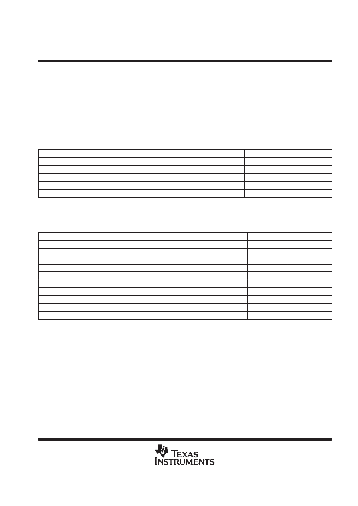
recommended operating conditions
MIN NOM MAX UNIT
Supply voltage range (AVDD, DVDD) 2.7 3.0 3.3 Vdc
Operating temperature range –25 85 °C
Digital I/O voltage with respect to DV
SS
–0.3 DVDD + 0.3 Vdc
Analog I/O voltage with respect to AV
SS
–0.3 AVDD + 0.3 V
Difference between any A VDD or DV
DD
0.3 V
electrical characteristics over recommended operating free-air temperature range (unless
otherwise noted)
digital inputs and outputs
PARAMETER
MIN TYP MAX UNIT
Low-level output current with digital pad lower than 0.1 V (CMOS) 0 40 µA
Low-level output current with digital pad lower than 0.4 V (TTL) 0 1 mA
High-level output current with digital pad higher than VDD–0.1 V (CMOS) –40 0 µA
High-level output current with digital pad higher than VDD–0.4 V (TTL) –1 0 mA
Minimum high-level input voltage, V
IH
Vdd–0.3 V
Maximum low level input voltage, V
IL
Vss+0.3 V
Output current on high impedance state outputs –15 15 µA
Input current (any input) when input high –1 µA
Input current (standard inputs) when input low 1 µA
Input current (inputs with pullup TMS, TDI ,TEST1 ,TEST2) when input low 15 µA

TCM4400E
GSM/DCS BASEBAND AND VOICE A/D
AND D/A RF INTERFACE CIRCUIT
SLWS082A – JULY 1999 – REVISED MARCH 2000
8
POST OFFICE BOX 655303 • DALLAS, TEXAS 75265
electrical characteristics over recommended operating free-air temperature range (unless
otherwise noted) (continued)
voltage references
REFERENCE MIN TYP MAX
UNIT
VGAP Voltage on band gap (used for all other references) 1.16 1.22 1.28 Vdc
Band gap output resistance 200 KΩ
Band gap external decoupling capacitance 0.1 µF
Band gap start time ( bit CHGUP=0 ) 100 ms
Band gap start time ( bit CHGUP=1) 2.5 ms
VREF Voltage reference of GMSK internal ADC and DAC : V
VREF
1.66 1.75 1.84 Vdc
Voltage reference output resistance 200 KΩ
Voltage reference external decoupling capacitance 0.1 µF
Voltage reference start time ( bit CHGUP=0 ) 300 ms
Voltage reference start time ( bit CHGUP=1) 10 ms
VMID Common-mode reference for baseband uplink: V
VMID
(Bit SELVMID=0) –10% Vdd/2 10% Vdc
Common-mode reference for baseband uplink: V
VMID
(Bit SELVMID=1) 1.25 1.35 1.45 Vdc
Load resistance on Vmid output 10 KΩ
MICBIAS Microphone-driving voltage (Bit MICBIAS=0) 1.80 2.00 2.20 Vdc
Microphone-driving voltage(Bit MICBIAS=1) 2.25 2.5 2.75 Vdc
Microphone-bias current drive capability (Bit MICBIAS= 1) 450 500 µA
Microphone-bias current drive capability (Bit MICBIAS=0 ) 350 400 µA
ADCMID DC bias reference of the auxiliary ADCs –10% Vdd/2 10% Vdc
ADCMID external decoupling capacitance 0.1 µF
IBIAS Bias current adjust external resistance 100 KΩ
master clock input (MCLK)
PARAMETER MIN NOM MAX UNIT
Master clock signal frequency 13 MHz
Master clock duty cycle (Sinewave) 40% 60%
Maximum peak-to-peak amplitude 1.3 Vpp
Minimum peak-to-peak amplitude 0.5 Vpp
Common-mode input voltage VSS +0.5 VDD –0.5 Vdc
Input resistance at 13MHz (MCLK to ground) 4.1 5 6.5 KΩ
Input capacitance at 13 MHz (MCLK to ground) 12.5 15 18 pf
baseband uplink path
PARAMETER TEST CONDITIONS MIN TYP MAX UNIT
I and Q D/A converters resolution 8 bit
Dynamic range on each output Centered on V
VMID
V
VREF
Vpp
Differential output dynamic range with OUTLEV bit = 0
†
BULQP-BULQN or BULIP-BULIN 2xV
VREF
Vpp
Differential output dynamic range with OUTLEV bit = 1
†
BULQP-BULQN or BULIP-BULIN 8/15 x V
VREF
Vpp
Output load resistance, differential 10 kΩ
Output load capacitance, differential 50 pF
Output common-mode voltage Programmable by bit SELVMID V
VMID
V
I & Q output state in power down Hi-Z
†
Initial value after reset and at beginning of each burst are BULIP–BULIN=V
REF
and BULQP–BULQN=0 corresponding to a phase angle of 0°.
TCM4400E
GSM/DCS BASEBAND AND VOICE A/D
AND D/A RF INTERFACE CIRCUIT
SLWS082A – JULY 1999 – REVISED MARCH 2000
9
POST OFFICE BOX 655303 • DALLAS, TEXAS 75265
electrical characteristics over recommended operating free-air temperature range (unless
otherwise noted) (continued)
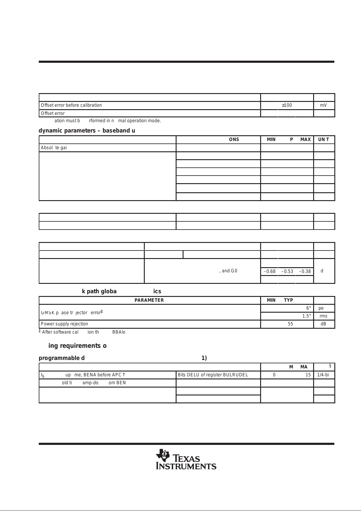
dc accuracy – baseband uplink path
PARAMETER MIN TYP MAX UNIT
Offset error before calibration
±100
mV
Offset error after calibration
†
–7
0
7
mV
†
Calibration must be performed in normal operation mode.
dynamic parameters – baseband uplink path
PARAMETER TEST CONDITIONS MIN TYP MAX UNIT
Absolute gain error relative to V
VREF
Measured with 67.7 kHz sinewave –1.5 0 1.5 dB
100 kHz –3 dB
200 kHz –34 dB
Maximum output random modulation spectrum relative to in-band
250 kHz –37 dB
average level. Measured by average
FFT
s of random bursts using
a
window with 30 kHz bandwidth.
400 kHz –65 dB
a window with 30 kHz bandwidth
.
600 KHz –72 dB
800 KHz –72 dB
smoothing filters characteristics – baseband uplink path
PARAMETER TEST CONDITIONS MIN TYP MAX UNIT
Group delay 0 Hz to 100 kHz 1.5 µs
I and Q channels gain matching – baseband uplink path
PARAMETER TEST CONDITIONS MIN TYP MAX UNIT
Gain matching between channels
0 Hz to 96 kHz
Measured on 67.7 kHZ sinewave
–1
0
1
dB
–0.42
–0.27
–0.12
I and Q gain unbalance
Programmable with bits IQSEL, G1, and G0
–0.68
–0.53
–0.38
dB
–0.93
–0.78
–0.63
baseband uplink path global characteristics
PARAMETER MIN TYP MAX UNIT
6° peak
GMSK ph
ase trajectory error
‡
1.5° rms
Power supply rejection 55 dB
‡
After software calibration through BBAloop
timing requirements of baseband uplink path
programmable delays – baseband uplink path (see Figure 1)
MIN NOM MAX UNIT
§
t
su1
Setup time, BENA before APC↑ Bits DELU of register BULRUDEL 0 15 1/4-bit
t
h1
Hold time, ramp-down from BENA low Bits DELD of register BULRUDEL 0 15 1/4-bit
Bit APCSPD = 0
1/16-bit
t
r
,
tfTransition time, APC
Bit APCSPD = 1
0
64
1/8-bit
§
Bit is relative to GSM bit = 1/270 kHz. Units can be a fractional part of the GSM bit as noted. Values in the above table are given for system
information only.

TCM4400E
GSM/DCS BASEBAND AND VOICE A/D
AND D/A RF INTERFACE CIRCUIT
SLWS082A – JULY 1999 – REVISED MARCH 2000
10
POST OFFICE BOX 655303 • DALLAS, TEXAS 75265
timing requirements of baseband uplink path (continued)
fixed delays – baseband uplink path (see Figure 1)
MIN NOM MAX UNIT
†
t
su2
Setup time, BULON↑ to BCAL↑ 15 µs
t
w1
Pulse duration, BCAL high 132 µs
t
su3
Setup time, BCAL low before BENA↑ 0 µs
t
w2
Pulse duration, BENA high N effective duration of burst controlled by BENA N–32 1/4-bit
t
h2
Hold time, modulation low after BENA low 32 1/4 bit
t
h3
Hold time, BULON↓ after APC low 1 bit
t
dd(mod)
Input-to-output modulator delay (Digital delay of modulator) 1.5 bit
†
Bit is relative to GSM bit = 1/270 kHz. Units can be a fractional part of the GSM bit as noted. Values in the above table are given for system
information only.
baseband downlink path
PARAMETER TEST CONDITIONS MIN TYP MAX UNIT
Dynamic range on each input
Centered on external common
mode (V
BDLCOM
)
V
VREF
Vpp
Differential input dynamic range DLQP–DLQN or DLIP–DLIN 2*V
VREF
Vpp
Differential input resistance at BDLQP–BDLQN or
BDLIP–BDLIN
130 200 270 kΩ
Differential input capacitance at BDLQP–BDLQN or
BDLIP–BDLIN
1.5 4 6.5 pF
Single ended input resistance at BDLQPor BDLQN or BDLIP
or BDLIN to ground.
90 130 180 kΩ
Single ended input capacitance at BDLQP or BDLQN or
BDLIP or BDLIN to ground.
6 8 12 pF
External common-mode input voltage: V
BDLCOM
0.8 VDD/2 VDD–0.8 V
Range of digital output data
Maximum digital code value on
16-bit I and Q samples.
±21060
dc accuracy – baseband downlink path
PARAMETER TEST CONDITIONS MIN TYP MAX UNIT
Offset error before calibration
‡
–60 0 60 LSB
Offset error after calibration, ± 21 on 16-bit I and Q words
‡
–2 0 2 LSB
Offset correction range Full scale
‡
The LSB corresponds to the one of the ADC which is specified with 66 dB dynamic range (±1024),which means 11-bit, but the output data bits
are transmitted through the serial interface with 16-bit words. On top of that, the decimation ratio of 24 (6.5 MHz/270 kHz) makes the maximum
code on a 16-bit word to be 21060 instead of 32767. So one LSB of the ADC corresponds to a value of 21060/1024 = 20.57 on the 16-bit output
serial words on I and Q.
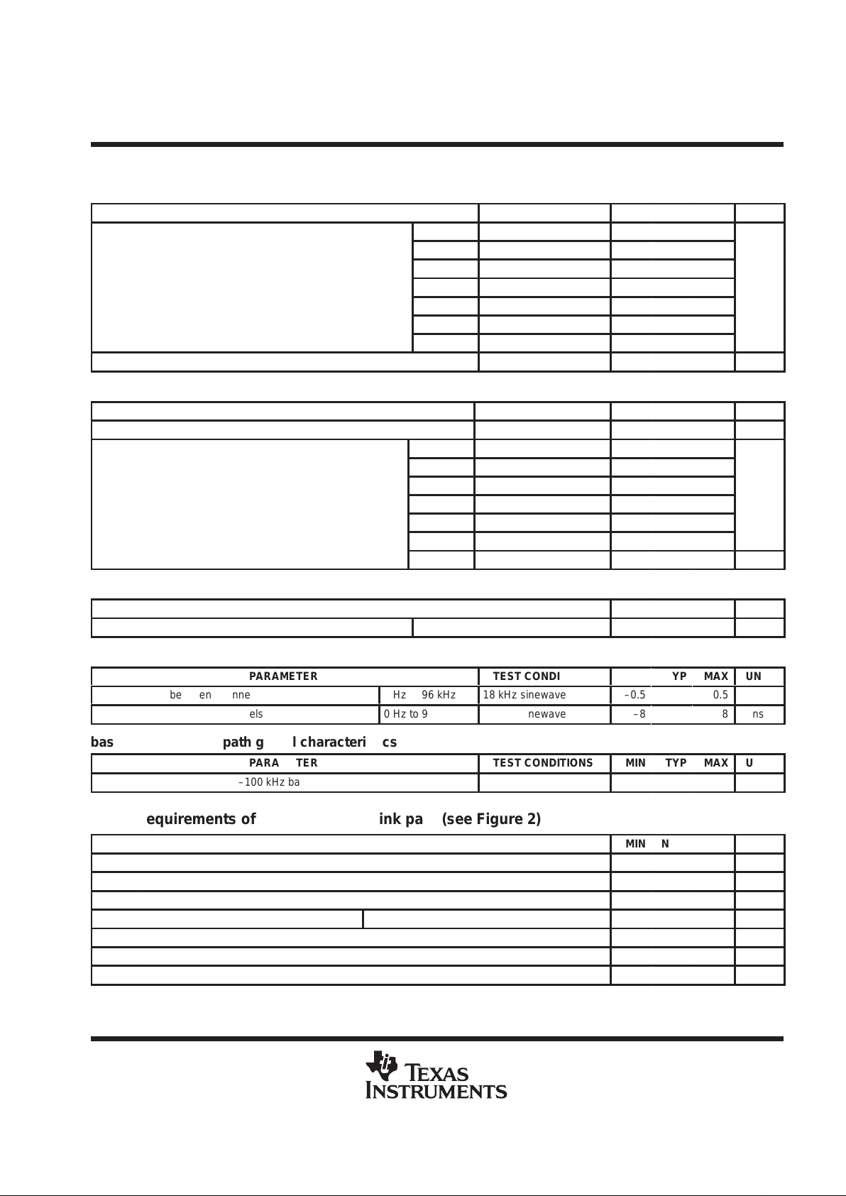
channel characteristics
frequency response – baseband downlink path
PARAMETER MIN TYP MAX UNIT
< 67.5 Hz –0.3 0.25
67.5 kHz –0.3 0.25
p
p
96 kHz –4 0.3
Frequency response of the total path with values referenced to 18 kH
z
135 kHz –40
dB
200 kHz –40
400 kHz –40
TCM4400E
GSM/DCS BASEBAND AND VOICE A/D
AND D/A RF INTERFACE CIRCUIT
SLWS082A – JULY 1999 – REVISED MARCH 2000
11
POST OFFICE BOX 655303 • DALLAS, TEXAS 75265
channel characteristics (continued)
SNR vs signal level–baseband downlink path
PARAMETER TEST CONDITIONS MIN TYP MAX UNIT
–50 dBm0 200 kHz bandwidth 21
–40 dBm0 26
–30 dBm0 36
Signal level
–20 dBm0 46
dB
–10 dBm0 50
–5 dBm0 55
0 dBm0 30
Idle channel noise, 0 Hz –200 kHz –66 dBm0
gain characteristics of the baseband downlink path
PARAMETER TEST CONDITIONS MIN TYP MAX UNIT
Absolute gain error relative to V
VREF
at –10 dBm0 and 18 kHz –11 –10 –9 dB
0 dBm0 –0.25 0.25
–5 dBm0 –0.25 0.25
–10 dBm0 Reference level 0
Gain t
racking error. Over the range 3 dBm0 to –50 dBm0 at
–
–20 dBm0 –0.25 0.25
dB
18 kHz with reference 10 dBm0
–30 dBm0 –0.25 0.25
–40 dBm0 –0.25 0.25
–50 dBm0 –0.50 0.50 dB
group delay – baseband downlink path
PARAMETER MIN TYP MAX UNIT
Group delay 0 Hz to 100 kHz 28 µs
I and Q channels matching – baseband downlink path
PARAMETER
TEST CONDITIONS
MIN
TYP
MAX
UNIT
Gain matching between channels
0 Hz to 96 kHz
18 kHz sinewave
–0.5
0.5
dB
Delay matching between channels
0 Hz to 96 kHz
18 kHz sinewave
–8
8
ns
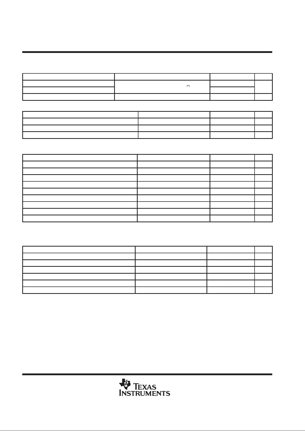
baseband downlink path global characteristics
PARAMETER TEST CONDITIONS MIN TYP MAX UNIT
Power supply rejection, 0 Hz –100 kHz band 70 dB
timing requirements of baseband downlink path (see Figure 2)
MIN NOM MAX UNIT
†
t
su4
Setup time, BDLON↑ to BCAL↑ 5 µs
t
w3
Pulse duration, BCAL 60 µs
t
su5
Setup time BCAL low before BENA↑ 0 µs
t
w4
Pulse duration, BENA high N ef fective duration of burst controlled by BENA N 1/4-bit
t
su6
Setup time, BENA↑ before DATAOUT V ALID 24.3 28 µs
t
h4
Hold time, DATAOUT VALID after BENA↓ 3.7 µs
t
h5
Hold time, BDLON low after BENA low 0 µs
†
Values in the above table are given for system information only.
TCM4400E
GSM/DCS BASEBAND AND VOICE A/D
AND D/A RF INTERFACE CIRCUIT
SLWS082A – JULY 1999 – REVISED MARCH 2000
12
POST OFFICE BOX 655303 • DALLAS, TEXAS 75265
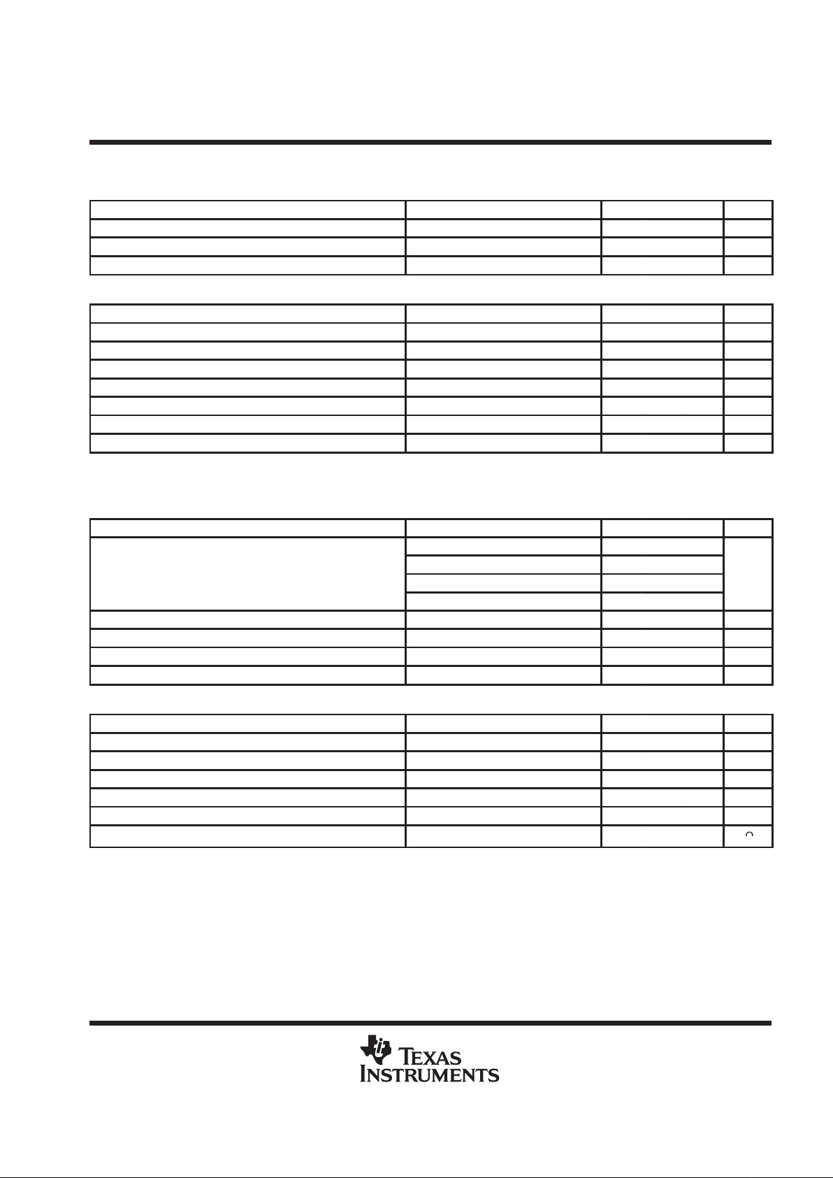
automatic power control (APC)
APC level (8-bit DAC)
PARAMETER TEST CONDITIONS MIN TYP MAX UNIT
Integral nonlinearity (best fitting)
p
p
–1 1
Differential nonlinearity
Shaper at maximum full scale Load 10 kΩ, 50 pF
–1 1
LSB
Settling time 10 µs
APC shaper (5-bit DAC)
PARAMETER TEST CONDITIONS MIN TYP MAX UNIT
Integral nonlinearity (best fitting ) –1 1 LSB
Differential nonlinearity –1 1 LSB
Settling time
†
1 µs
†
Value given for system information only.
APC output stage
PARAMETER TEST CONDITIONS MIN TYP MAX UNIT
Output voltage at shape=31 & level =255 2.0 2.2 2.4 V
Output voltage at shape=0 & level=xx Bit APCMODE = 0 0 20 mV
Output voltage at shape=0 & level =xx Bit APCMODE =1 80 120 160 mV
Output voltage at shape=xx & level = 0 0 5 mV
Output voltage in power-down 0 V
DC power supply sensitivity 1%
Output impedance in power-down 20 Ω
Load resistance 10 kΩ
Load capacitance 50 pF
monitoring ADC
10-bit ADC
PARAMETER TEST CONDITIONS MIN TYP MAX UNIT
Integral nonlinearity (Best fitting) Input signal range < 0.95 V
VREF
–4 4 LSB
Differential nonlinearity Input signal range < 0.95 V
VREF
–2 2 LSB
Conversion time
†
10 µs
Input range 0 V
VREF
V
Input leakage current –10 10 µA
Input capacitance 25 pF
†
Value given for system information only.
TCM4400E
GSM/DCS BASEBAND AND VOICE A/D
AND D/A RF INTERFACE CIRCUIT
SLWS082A – JULY 1999 – REVISED MARCH 2000
13
POST OFFICE BOX 655303 • DALLAS, TEXAS 75265
automatic Gain Control (AGC)
AGC 10-bit DAC
PARAMETER TEST CONDITIONS MIN TYP MAX UNIT
Integral nonlinearity Best fitting line –1 1 LSB
Differential nonlinearity –1 1 LSB
Settling time From AUXAGC load 100 µs
AGC output stage
PARAMETER TEST CONDITIONS MIN TYP MAX UNIT
Output voltage with code max 1.9 2.2 2.4 V
Offset voltage with code 000 0.18 0.24 0.30 V
Output voltage in power down 0 V
DC power supply sensitivity 1%
Output impedance in power down 200 kΩ
Load resistance 10 kΩ
Load capacitance 50 pF
automatic frequency control (AFC)
AFC 13-bit DAC
PARAMETER TEST CONDITIONS MIN TYP MAX UNIT
AFCCK1=1 AFCCK0 = 1 2
p
AFCCK1=1 AFCCK0 = 0 1
Sampling frequenc
y,
f
s
AFCCK1=0 AFCCK0 = 1 0.5
MH
z
AFCCK1=0 AFCCK0 = 0 0.25
Integral nonlinearity from 0 to 75% output range Best fitting line ±1 LSB
Differential nonlinearity from 0 to 75% output range ±1 LSB
Settling time 1 µs
DC power-supply sensitivity Over power supply range 1%
AFC output stage
PARAMETER TEST CONDITIONS MIN TYP MAX UNIT
Internal output resistance (±30 % tolerance) 25 kΩ
External filtering capacitance 33 nF
Output voltage with code max 2.0 2.5 2.8 V
Output voltage with code min 0 3 6 mV
Output voltage in power down 0 V
p
p
p
Output impedance in power down
25
kΩ
TCM4400E
GSM/DCS BASEBAND AND VOICE A/D
AND D/A RF INTERFACE CIRCUIT
SLWS082A – JULY 1999 – REVISED MARCH 2000
14
POST OFFICE BOX 655303 • DALLAS, TEXAS 75265
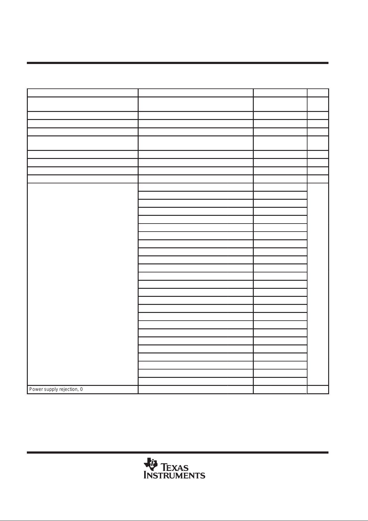
voice uplink path
global characteristics of voice uplink path
PARAMETER TEST CONDITIONS MIN TYP MAX UNIT
Maximum input range (MICP – MICN)
Inputs 3 dBm0 (maximum digital sample amplitude)
with PGA gain, set to 0dB (default value)
32.5 mVrms
Nominal reference level (MICP – MICN) –10 dBm0
Differential input resistance (MICP – MICN) 90 140 200 kΩ
Micro-amplifier gain 27 dB
Maximum input range at AUXI
Inputs 3 dBm0 (maximum digital sample amplitude)
with PGA gain, set to 0dB (default value)
365 mVrms
Nominal reference level at AUXI –10 dBm0
Input resistance at AUXI 140 220 300 kΩ
Auxi amplifier gain 6 dB
PGA absolute gain 4.6 dB
VULPGA code =10000 –12 dB –12.7 –12.2 –1 1.7
VULPGA code = 10111 –11 dB –11.3 –10.8 –10.3
VULPGA code = 11000 –10 dB –10.6 –10.1 –9.6
VULPGA code = 11001 –9 dB –9.5 –9 –8.5
VULPGA code = 11010 –8 dB –8.5 –8 –7.5
VULPGA code = 11011 –7 dB –7.5 –7 –6.5
VULPGA code = 00000 (default) –6 dB –6.7 –6.2 –5.7
VULPGA code = 00001 –5 dB –5.6 –5.1 –4.6
VULPGA code = 00010 –4 dB –4.6 –4.1 –3.6
VULPGA code = 00011 –3 dB –3.5 –3 –2.5
VULPGA code = 00100 –2 dB –2.4 –1.9 –1.4
VULPGA code = 00101 –1 dB –1.5 –1 –0.5
PGA gain step
VULPGA code = 00110 (ref) 0 dB 0
dB
VULPGA code = 00111 1 dB 0.7 1.2 1.7
VULPGA code = 01000 2 dB 1.4 1.9 2.4
VULPGA code = 01001 3 dB 2.6 3.1 3.6
VULPGA code = 01010 4 dB 3.6 4.1 4.6
VULPGA code = 01011 5 dB 4.5 5 5.5
VULPGA code = 01100 6 dB 5.3 5.8 6.3
VULPGA code = 10001 7 dB 6.4 6.9 7.4
VULPGA code = 10010 8 dB 7.4 7.9 8.4
VULPGA code = 10011 9 dB 8.6 9.1 9.6
VULPGA code = 10100 10 dB 9.6 10.1 10.6
VULPGA code = 10101 11 dB 10.5 11 11.5
VULPGA code = 10110 12 dB 11.5 12 12.5
Power supply rejection, 0 Hz –100 kHz band
70
dB

TCM4400E
GSM/DCS BASEBAND AND VOICE A/D
AND D/A RF INTERFACE CIRCUIT
SLWS082A – JULY 1999 – REVISED MARCH 2000
15
POST OFFICE BOX 655303 • DALLAS, TEXAS 75265
voice uplink path (continued)
frequency response of the voiceband uplink path
PARAMETER
TEST CONDITIONS
MIN TYP MAX UNIT
100 Hz –37.4 –20
150 Hz –25.9 –15
200 Hz –16.5 –10
300 Hz –2 –1.46 1
1000 Hz Reference point is 1000 Hz 0
Frequency response (Gain relative to reference gain at
2000 Hz –1.5 –0.58 1
qy ( g
1 kHz)
3000 Hz –1.5 –0.77 1
dB
3400 Hz –2 –1 1
3600 Hz –12.4 –6
3800 Hz –23.3 –18
4000 Hz –35 –30
>4600 Hz >–52 –40
psophometric SNR vs signal level of the voiceband uplink path
PARAMETER TEST CONDITIONS MIN TYP MAX UNIT
3 dBm0 35
0 dBm0 40
–5 dBm0 42
–10 dBm0 45
Signal to noise
+
distortion
–20 dBm0 42
dB
–30 dBm0 40
–40 dBm0 30
–45 dBm0 25
Maximum idle channel noise 0 Hz –4 kHz –72 dBm0
Crosstalk with the downlink path Downlink path loaded with 150 Ω –66 dB
gain characteristics of the voiceband uplink path
PARAMETER TEST CONDITIONS MIN TYP MAX UNIT
at 0dBm0 and 1KHz –1 1
Absolute gain error
at –10dBm0 and 1KHz –1 1 –10 –9
dB
3 dBm0 –0.25 0.25
0 dBm0 –0.25 0.25
–5 dBm0 –0.25 0.25
Gain tracking error. Over the range 3 dBm0 to –45 dBm0 at
–10 dBm0 Reference level 0
gg
1 kHz with reference –10 dBm0
–20 dBm0 –0.25 0.25
dB
–30 dBm0 –0.25 0.25
–40 dBm0 –0.35 0.35
–45 dBm0 –0.50 0.50
TCM4400E
GSM/DCS BASEBAND AND VOICE A/D
AND D/A RF INTERFACE CIRCUIT
SLWS082A – JULY 1999 – REVISED MARCH 2000
16
POST OFFICE BOX 655303 • DALLAS, TEXAS 75265
voice downlink path
global characteristics of voice downlink path
PARAMETER TEST CONDITIONS MIN TYP MAX UNIT
Maximum output swin
g
With 5% distortion and with 150 Ω 3.1 3.92
pp
Maximum out ut swing
(EARP – EARN)
With 5% distortion and with 33 Ω 1.2 1.5
Vpp
p
Output swing 3.9Vpp 120 150 Ω
Minimum output resistive load at EARP_EARN
Output swing 1.5Vpp 30 33 Ω
Maximum output capacitive load at EARP_EARN 100 pF
Earphone amplifier gain 0 dB
Earphone amplifier state in power down Hi-Z
Maximum output swing (AUXO), 5% distortion, maximum Load = 1 kΩ 1.6 1.96 Vpeak
Minimum output resistive load at AUXO AC coupled 1.0 1.2 kΩ
Maximum output capacitive load at AUXO 100 pF
Auxo amplifier gain –6 dB
Auxo amplifier state in power down Hi-Z
VOLCTL code = 010 –1 0 1
VOLCTL code = 110 –7 –6 –5
VOLCTL code = 000 (default & reference) –12
Volume control gains
VOLCTL code = 100 –19 –18 –17
dB
VOLCTL code = 011 –25 –24 –23
VOLCTL code =101 or 001 or 111 (mute) –40
VDLPGA code = 0000 (default) –6 dB –6.5 –6.0 –5.5
VDLPGA code = 0001 –5 dB –5.5 –5.0 –4.5
VDLPGA code = 0010 –4 dB –4.5 –4.0 –3.5
VDLPGA code = 0011 –3 dB –3.7 –3.2 –2.7
VDLPGA code = 0100 –2 dB –2.3 –1.8 –1.3
VDLPGA code = 0101 –1 dB –1.7 –1.2 –0.7
PGA gain steps
VDLPGA code = 0110 (ref.) 0 dB 0
dB
VDLPGA code = 0111 1 dB 0.5 1.0 1.5
VDLPGA code = 1000 2 dB 1.4 1.9 2.4
VDLPGA code = 1001 3 dB 2.6 3.1 3.6
VDLPGA code = 1010 4 dB 3.4 3.9 4.4
VDLPGA code = 1011 5 dB 4.3 4.8 5.3
VDLPGA code = 1100 6 dB 5.5 6.0 6.5
VDLST code = 1101 –23 dB –24.6 –24.1 –22.6
VDLST code = 1100 –20 dB –21.1 –20.6 –18.5
VDLST code = 0110 –17 dB –18.3 –17.8 –17.3
VDLST code = 0010 –14 dB –14.8 –14.3 –13.8
p
VDLST code = 0111 –11 dB –12.3 –11.8 –11.3
Sidetone gain steps
VDLST code = 0011 –8 dB –8.8 –8.3 –7.8
dB
VDLST code = 0000 (ref.) –5 dB –5.9 –4.8 –4.3
VDLST code = 0100 –2 dB –2.1 –1.6 –1.1
VDLST code = 0001 1 dB 0.7 1.2 1.7
VDLST code = 1000 Mute –55 –50
Power supply rejection, 0 Hz –100 kHz In the band 60 dB
NOTE: All parameters are given for a 150 Ω load, unless specified.
TCM4400E
GSM/DCS BASEBAND AND VOICE A/D
AND D/A RF INTERFACE CIRCUIT
SLWS082A – JULY 1999 – REVISED MARCH 2000
17
POST OFFICE BOX 655303 • DALLAS, TEXAS 75265
voice downlink path (continued)
frequency response of the voiceband downlink path
PARAMETER TEST CONDITIONS MIN TYP MAX UNIT
100 Hz –5.8 –5
150 Hz
–3.6 –2
200 Hz –2.5 1
300 Hz –3 –1.4 1
1000 Hz Reference point 0
Frequency response (Gain relative to
2000 Hz –1 –0.6 1
qy (
reference gain at 1 kHz)
3000 Hz –1 –0.15 1
dB
3400 Hz –3 –0.35 1
3600 Hz
–9.0 –6
3800 Hz
–21.0 –15
4000 Hz –32.0 –28
>4600 Hz –60.0
psophometric SNR vs signal level of the voiceband downlink path
PARAMETER TEST CONDITIONS MIN TYP MAX UNIT
–45 dBm0 25
–40 dBm0 30
–30 dBm0 40
–20 dBm0 42
Si
gnal leve
l
–10 dBm0 45
dB
–5 dBm0 42
0 dBm0
40
3 dBm0 35
Idle channel noise, 0 Hz –4 kHz –71 dBm
Crosstalk with the uplink path –50 dB
gain characteristics of the voiceband downlink path
PARAMETER TEST CONDITIONS MIN TYP MAX UNIT
at 0 dbm0 and 1 kHz –1.8 0 0.2
Absolute gain error
at –10 dbm0 and 1 kHz –11.8 –10 –9.8
dB
3 dBm0 –0.25 0.25
0 dBm0 –0.25 0.25
–5 dBm0 –0.25 0.25
Gain tracking error. Over the range 3 dBm0 to –45 dBm0 at
–10 dBm0 Reference level 0
1 kHz with reference –10 dBm0 PGA gain
=
0dB. Volume
control = –12 dB
–20 dBm0 –0.25 0.25
dB
control 12 dB
–30 dBm0 –0.25 0.25
–40 dBm0 –0.35 0.35
–45 dBm0 –0.50 0.50
TCM4400E
GSM/DCS BASEBAND AND VOICE A/D
AND D/A RF INTERFACE CIRCUIT
SLWS082A – JULY 1999 – REVISED MARCH 2000
18
POST OFFICE BOX 655303 • DALLAS, TEXAS 75265
power consumption
consumption by circuit block
CIRCUIT BLOCK TEST CONDITIONS MIN TYP MAX UNIT
ADC
DVDD3 0.013
AFC
AVDD3 0.021
mA
AVDD5 0.027
AVDD3 0.054
AGC
AVDD5 0.683
mA
DVDD3 0.133
APC
AVDD3 0.108
mA
AVDD5 0.442
Auxiliary input stage AVDD4 2.240 mA
Auxiliary output stage A VDD4 1.550
Band gap AVDD1 0.163 mA
DVDD2 2.810
Baseband downlink
AVDD2 9.310
mA
p
DVDD2 0.460
Baseband uplink
AVDD2 4.910
mA
BBIF DVDD1 BDL Active 1.490 mA
Clock generator BBIF DVDD1 0.122 mA
Clock generator Idle DVDD1 0.204 mA
Clock generator TIIF DVDD1 0.181 mA
Clock generator VBIF DVDD1 0.144 mA
Digital modulator DVDD4 0.183 mA
Earphone output stage AVDD4 4.170 mA
Microphone input stage AVDD4 3.000 mA
DVDD4 1.380
Voiceband downlink
AVDD4 2.990
mA
p
DVDD4 1.200
Voiceband uplink
AVDD4 0.115
mA
current consumption for typical configurations
PARAMETER TEST CONDITIONS MIN TYP MAX UNIT
Deep power down
13-MHz clock applied; PWRDN active;
Band-gap voltage reference off
200 µA
Power down with AFC active AFC programmed with internal 50-kΩ and 1-MHz clock 0.7 1.1 mA
AFC + GMSK – Rx Paging 14 16 mA
Audio + GMSK – Tx + APC + AFC Transmit burst 19 21 mA
Audio + GMSK – Rx +AGC+ AFC Receive burst 27 30 mA
TCM4400E
GSM/DCS BASEBAND AND VOICE A/D
AND D/A RF INTERFACE CIRCUIT
SLWS082A – JULY 1999 – REVISED MARCH 2000
19
POST OFFICE BOX 655303 • DALLAS, TEXAS 75265
MCU serial interface timing requirements (see Figure 3)
PARAMETER MIN NOM MAX UNIT
t
su10
Setup time, UCLK stable before USEL↓ 20 ns
t
v1
Hold time, UDX valid after USEL↓ 20 ns
t
v2
Hold time, UDX valid after UCLK↑ 20 ns
t
h9
Sequential transfer delay between 16-bit word acquisition tw pulse duration, USEL high 3000 ns
t
h10
Hold time, UCLK↑ after USEL↓ 20 ns
t
h11
Hold time, UCLK unknown after USEL↑ 20 ns
t
su11
Setup time, data valid before UCLK↓ 20 ns
t
h12
Hold time, data valid after UCLK↓ 20 ns
t
c
Cycle time, ULCK 154 ns
DSP serial interface timing requirements (see Figure 4)
PARAMETER MIN NOM MAX UNIT
BCLKX BCLKX signal frequency ( Burst mode or Continuous mode depending on bit BCLKMODE) 13 MHz
BCLKX BCLKX duty cycle 40% 50% 60%
t
su12
Setup time, BFSX high before BCLKX ↓ 20 ns
t
h12
Hold time, BFSX high after BCLKX ↓ 20 ns
t
su13
Setup time, BDX valid before BCLKX ↓ 20 ns
t
h13
Hold time, BDX valid after BCLKX ↓ 20 ns
(Output BCLKDIR = 0) 4.33
BCLKR
BCLKR si
gnal frequency
(Input BCLKDIR = 1)
13
MH
z
BCLKR BCLKR duty cycle 40% 50% 60%
t
su14
Setup time, BFSR high before BCLKR ↓ 20 ns
t
h14
Hold time, BFSR high after BCLKR ↓ 20 ns
t
su16
Setup time, BDR valid before BCLKR ↓ 20 ns
t
h15
Setup time, BDR valid after BCLKR ↓ 20 ns
voice timing requirements (see Figure 5)
PARAMETER MIN NOM MAX UNIT
VCLK VCLK signal frequency ( Burst mode or Continuous mode depending on bit VCLKMODE) 520 kHz
VCLK VCLK duty cycle 40% 50% 60%
t
su7
Setup time, VFS high before VCLK ↓ 100 ns
t
h6
Hold time, VFS high after VCLK ↓ 100 ns
t
su8
Setup time, VDX valid before VCLK ↓ 100 ns
t
h8
Hold time, VDX valid after VCLK ↓ 100 ns
t
su9
Setup time, VDR valid before VCLK ↓ 100 ns
t
h7
Hold time, VDR valid after VCLK ↓ 100 ns
TCM4400E
GSM/DCS BASEBAND AND VOICE A/D
AND D/A RF INTERFACE CIRCUIT
SLWS082A – JULY 1999 – REVISED MARCH 2000
20
POST OFFICE BOX 655303 • DALLAS, TEXAS 75265
PARAMETER MEASUREMENT INFORMATION
uplink timing considerations
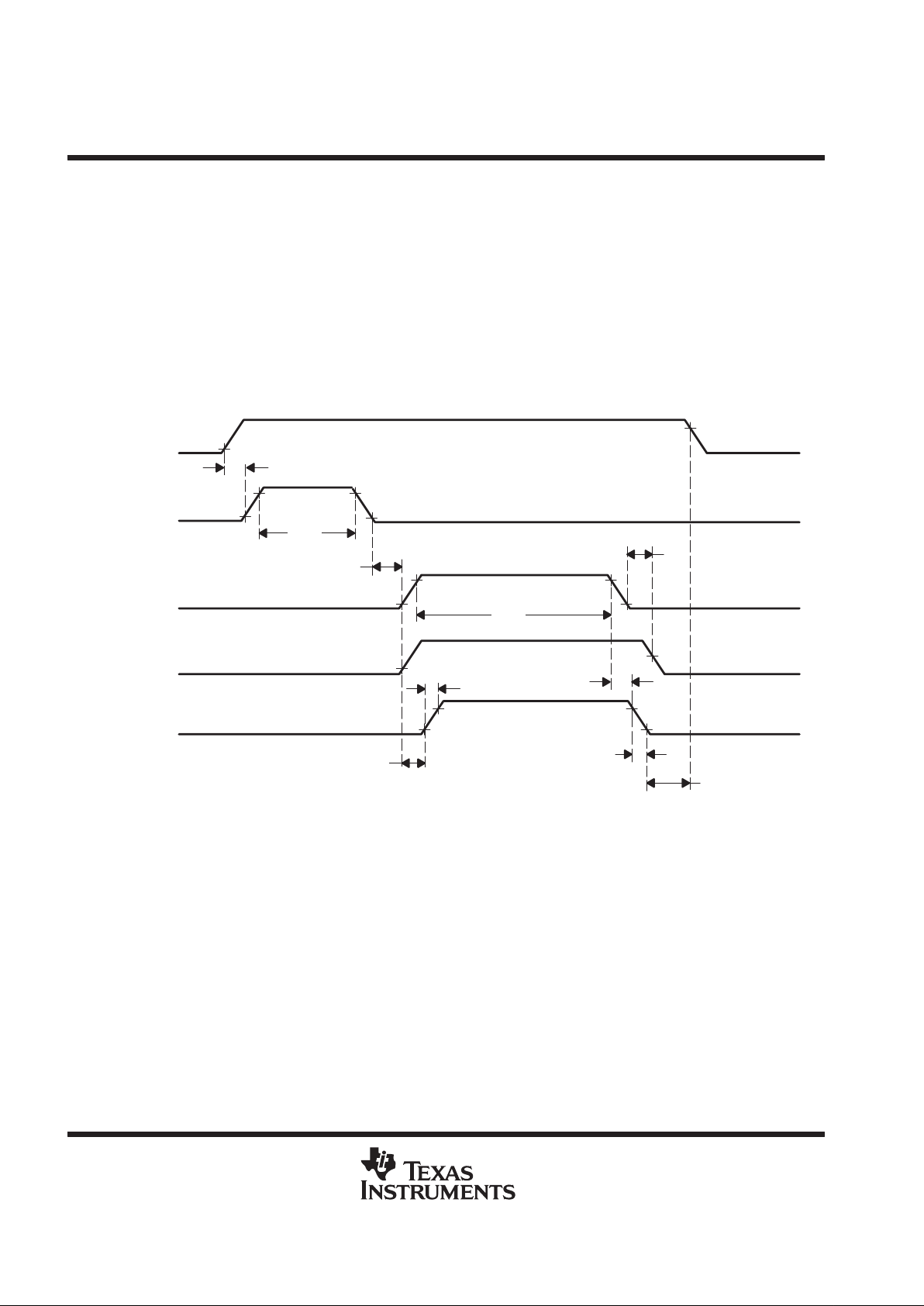
Figure 1 shows the timing diagram for the uplink operation.
Timing for power up, offset calibration, data transmission, and power ramp-up are driven by control bits applied
to BULON (base uplink on), BCAL (calibration) and BENA (enable). The burst content including guard bits, tail
bits, and data bits is sent by the DSP by way of the DSP interface and then stored by the TCM4400E in a burst
buffer. Transmission start is indicated by the control bit BENA when the BULON is active. The transmission,
sequencing, and power ramp-up are then controlled by an on-chip burst sequencer with a one-quarter-bit timing
accuracy. For a detailed description of the baseband in length path, see the functional description of the
baseband uplink path in the
Principles of Operation
section.
t
su2
t
w1
t
su3
t
h2
t
su1
t
r1
t
h1
t
f1
t
h3
BULON
BCAL
BENA
MODULATION
APC
t
w2
Figure 1. Uplink Timing Diagram
 Loading...